EP4283671A2 - Halbleiterbauelement und herstellungsverfahren dafür - Google Patents
Halbleiterbauelement und herstellungsverfahren dafür Download PDFInfo
- Publication number
- EP4283671A2 EP4283671A2 EP23170173.1A EP23170173A EP4283671A2 EP 4283671 A2 EP4283671 A2 EP 4283671A2 EP 23170173 A EP23170173 A EP 23170173A EP 4283671 A2 EP4283671 A2 EP 4283671A2
- Authority
- EP
- European Patent Office
- Prior art keywords
- layer structure
- soc
- semiconductor device
- conductive
- bridge die
- Prior art date
- Legal status (The legal status is an assumption and is not a legal conclusion. Google has not performed a legal analysis and makes no representation as to the accuracy of the status listed.)
- Pending
Links
Images











Classifications
-
- H—ELECTRICITY
- H10—SEMICONDUCTOR DEVICES; ELECTRIC SOLID-STATE DEVICES NOT OTHERWISE PROVIDED FOR
- H10W—GENERIC PACKAGES, INTERCONNECTIONS, CONNECTORS OR OTHER CONSTRUCTIONAL DETAILS OF DEVICES COVERED BY CLASS H10
- H10W70/00—Package substrates; Interposers; Redistribution layers [RDL]
- H10W70/60—Insulating or insulated package substrates; Interposers; Redistribution layers
- H10W70/62—Insulating or insulated package substrates; Interposers; Redistribution layers characterised by their interconnections
- H10W70/65—Shapes or dispositions of interconnections
-
- H—ELECTRICITY
- H10—SEMICONDUCTOR DEVICES; ELECTRIC SOLID-STATE DEVICES NOT OTHERWISE PROVIDED FOR
- H10W—GENERIC PACKAGES, INTERCONNECTIONS, CONNECTORS OR OTHER CONSTRUCTIONAL DETAILS OF DEVICES COVERED BY CLASS H10
- H10W70/00—Package substrates; Interposers; Redistribution layers [RDL]
- H10W70/60—Insulating or insulated package substrates; Interposers; Redistribution layers
-
- H—ELECTRICITY
- H10—SEMICONDUCTOR DEVICES; ELECTRIC SOLID-STATE DEVICES NOT OTHERWISE PROVIDED FOR
- H10W—GENERIC PACKAGES, INTERCONNECTIONS, CONNECTORS OR OTHER CONSTRUCTIONAL DETAILS OF DEVICES COVERED BY CLASS H10
- H10W70/00—Package substrates; Interposers; Redistribution layers [RDL]
- H10W70/01—Manufacture or treatment
- H10W70/05—Manufacture or treatment of insulating or insulated package substrates, or of interposers, or of redistribution layers
- H10W70/08—Manufacture or treatment of insulating or insulated package substrates, or of interposers, or of redistribution layers by depositing layers on the chip or wafer, e.g. "chip-first" RDLs
- H10W70/09—Manufacture or treatment of insulating or insulated package substrates, or of interposers, or of redistribution layers by depositing layers on the chip or wafer, e.g. "chip-first" RDLs extending onto an encapsulation that laterally surrounds the chip or wafer, e.g. fan-out wafer level package [FOWLP] RDLs
-
- H—ELECTRICITY
- H10—SEMICONDUCTOR DEVICES; ELECTRIC SOLID-STATE DEVICES NOT OTHERWISE PROVIDED FOR
- H10W—GENERIC PACKAGES, INTERCONNECTIONS, CONNECTORS OR OTHER CONSTRUCTIONAL DETAILS OF DEVICES COVERED BY CLASS H10
- H10W70/00—Package substrates; Interposers; Redistribution layers [RDL]
- H10W70/60—Insulating or insulated package substrates; Interposers; Redistribution layers
- H10W70/611—Insulating or insulated package substrates; Interposers; Redistribution layers for connecting multiple chips together
-
- H—ELECTRICITY
- H10—SEMICONDUCTOR DEVICES; ELECTRIC SOLID-STATE DEVICES NOT OTHERWISE PROVIDED FOR
- H10W—GENERIC PACKAGES, INTERCONNECTIONS, CONNECTORS OR OTHER CONSTRUCTIONAL DETAILS OF DEVICES COVERED BY CLASS H10
- H10W70/00—Package substrates; Interposers; Redistribution layers [RDL]
- H10W70/60—Insulating or insulated package substrates; Interposers; Redistribution layers
- H10W70/611—Insulating or insulated package substrates; Interposers; Redistribution layers for connecting multiple chips together
- H10W70/616—Insulating or insulated package substrates; Interposers; Redistribution layers for connecting multiple chips together package substrates, interposers or redistribution layers combined with bridge chips
- H10W70/618—Insulating or insulated package substrates; Interposers; Redistribution layers for connecting multiple chips together package substrates, interposers or redistribution layers combined with bridge chips the bridge chips being embedded in the package substrates, interposers or redistribution layers
-
- H—ELECTRICITY
- H10—SEMICONDUCTOR DEVICES; ELECTRIC SOLID-STATE DEVICES NOT OTHERWISE PROVIDED FOR
- H10W—GENERIC PACKAGES, INTERCONNECTIONS, CONNECTORS OR OTHER CONSTRUCTIONAL DETAILS OF DEVICES COVERED BY CLASS H10
- H10W70/00—Package substrates; Interposers; Redistribution layers [RDL]
- H10W70/60—Insulating or insulated package substrates; Interposers; Redistribution layers
- H10W70/62—Insulating or insulated package substrates; Interposers; Redistribution layers characterised by their interconnections
- H10W70/63—Vias, e.g. via plugs
- H10W70/635—Through-vias
-
- H—ELECTRICITY
- H10—SEMICONDUCTOR DEVICES; ELECTRIC SOLID-STATE DEVICES NOT OTHERWISE PROVIDED FOR
- H10W—GENERIC PACKAGES, INTERCONNECTIONS, CONNECTORS OR OTHER CONSTRUCTIONAL DETAILS OF DEVICES COVERED BY CLASS H10
- H10W74/00—Encapsulations, e.g. protective coatings
- H10W74/01—Manufacture or treatment
-
- H—ELECTRICITY
- H10—SEMICONDUCTOR DEVICES; ELECTRIC SOLID-STATE DEVICES NOT OTHERWISE PROVIDED FOR
- H10W—GENERIC PACKAGES, INTERCONNECTIONS, CONNECTORS OR OTHER CONSTRUCTIONAL DETAILS OF DEVICES COVERED BY CLASS H10
- H10W74/00—Encapsulations, e.g. protective coatings
- H10W74/10—Encapsulations, e.g. protective coatings characterised by their shape or disposition
- H10W74/111—Encapsulations, e.g. protective coatings characterised by their shape or disposition the semiconductor body being completely enclosed
- H10W74/121—Encapsulations, e.g. protective coatings characterised by their shape or disposition the semiconductor body being completely enclosed by multiple encapsulations, e.g. by a thin protective coating and a thick encapsulation
-
- H—ELECTRICITY
- H10—SEMICONDUCTOR DEVICES; ELECTRIC SOLID-STATE DEVICES NOT OTHERWISE PROVIDED FOR
- H10W—GENERIC PACKAGES, INTERCONNECTIONS, CONNECTORS OR OTHER CONSTRUCTIONAL DETAILS OF DEVICES COVERED BY CLASS H10
- H10W90/00—Package configurations
-
- H—ELECTRICITY
- H10—SEMICONDUCTOR DEVICES; ELECTRIC SOLID-STATE DEVICES NOT OTHERWISE PROVIDED FOR
- H10W—GENERIC PACKAGES, INTERCONNECTIONS, CONNECTORS OR OTHER CONSTRUCTIONAL DETAILS OF DEVICES COVERED BY CLASS H10
- H10W70/00—Package substrates; Interposers; Redistribution layers [RDL]
- H10W70/099—Connecting interconnections to insulating or insulated package substrates, interposers or redistribution layers
-
- H—ELECTRICITY
- H10—SEMICONDUCTOR DEVICES; ELECTRIC SOLID-STATE DEVICES NOT OTHERWISE PROVIDED FOR
- H10W—GENERIC PACKAGES, INTERCONNECTIONS, CONNECTORS OR OTHER CONSTRUCTIONAL DETAILS OF DEVICES COVERED BY CLASS H10
- H10W70/00—Package substrates; Interposers; Redistribution layers [RDL]
- H10W70/60—Insulating or insulated package substrates; Interposers; Redistribution layers
- H10W70/611—Insulating or insulated package substrates; Interposers; Redistribution layers for connecting multiple chips together
- H10W70/614—Insulating or insulated package substrates; Interposers; Redistribution layers for connecting multiple chips together the multiple chips being integrally enclosed
-
- H—ELECTRICITY
- H10—SEMICONDUCTOR DEVICES; ELECTRIC SOLID-STATE DEVICES NOT OTHERWISE PROVIDED FOR
- H10W—GENERIC PACKAGES, INTERCONNECTIONS, CONNECTORS OR OTHER CONSTRUCTIONAL DETAILS OF DEVICES COVERED BY CLASS H10
- H10W70/00—Package substrates; Interposers; Redistribution layers [RDL]
- H10W70/60—Insulating or insulated package substrates; Interposers; Redistribution layers
- H10W70/62—Insulating or insulated package substrates; Interposers; Redistribution layers characterised by their interconnections
- H10W70/63—Vias, e.g. via plugs
-
- H—ELECTRICITY
- H10—SEMICONDUCTOR DEVICES; ELECTRIC SOLID-STATE DEVICES NOT OTHERWISE PROVIDED FOR
- H10W—GENERIC PACKAGES, INTERCONNECTIONS, CONNECTORS OR OTHER CONSTRUCTIONAL DETAILS OF DEVICES COVERED BY CLASS H10
- H10W72/00—Interconnections or connectors in packages
- H10W72/071—Connecting or disconnecting
- H10W72/072—Connecting or disconnecting of bump connectors
-
- H—ELECTRICITY
- H10—SEMICONDUCTOR DEVICES; ELECTRIC SOLID-STATE DEVICES NOT OTHERWISE PROVIDED FOR
- H10W—GENERIC PACKAGES, INTERCONNECTIONS, CONNECTORS OR OTHER CONSTRUCTIONAL DETAILS OF DEVICES COVERED BY CLASS H10
- H10W72/00—Interconnections or connectors in packages
- H10W72/071—Connecting or disconnecting
- H10W72/072—Connecting or disconnecting of bump connectors
- H10W72/07202—Connecting or disconnecting of bump connectors using auxiliary members
- H10W72/07204—Connecting or disconnecting of bump connectors using auxiliary members using temporary auxiliary members, e.g. sacrificial coatings
- H10W72/07207—Temporary substrates, e.g. removable substrates
-
- H—ELECTRICITY
- H10—SEMICONDUCTOR DEVICES; ELECTRIC SOLID-STATE DEVICES NOT OTHERWISE PROVIDED FOR
- H10W—GENERIC PACKAGES, INTERCONNECTIONS, CONNECTORS OR OTHER CONSTRUCTIONAL DETAILS OF DEVICES COVERED BY CLASS H10
- H10W72/00—Interconnections or connectors in packages
- H10W72/071—Connecting or disconnecting
- H10W72/073—Connecting or disconnecting of die-attach connectors
-
- H—ELECTRICITY
- H10—SEMICONDUCTOR DEVICES; ELECTRIC SOLID-STATE DEVICES NOT OTHERWISE PROVIDED FOR
- H10W—GENERIC PACKAGES, INTERCONNECTIONS, CONNECTORS OR OTHER CONSTRUCTIONAL DETAILS OF DEVICES COVERED BY CLASS H10
- H10W72/00—Interconnections or connectors in packages
- H10W72/071—Connecting or disconnecting
- H10W72/073—Connecting or disconnecting of die-attach connectors
- H10W72/07302—Connecting or disconnecting of die-attach connectors using an auxiliary member
- H10W72/07304—Connecting or disconnecting of die-attach connectors using an auxiliary member the auxiliary member being temporary, e.g. a sacrificial coating
- H10W72/07307—Connecting or disconnecting of die-attach connectors using an auxiliary member the auxiliary member being temporary, e.g. a sacrificial coating the auxiliary member being a temporary substrate, e.g. a removable substrate
-
- H—ELECTRICITY
- H10—SEMICONDUCTOR DEVICES; ELECTRIC SOLID-STATE DEVICES NOT OTHERWISE PROVIDED FOR
- H10W—GENERIC PACKAGES, INTERCONNECTIONS, CONNECTORS OR OTHER CONSTRUCTIONAL DETAILS OF DEVICES COVERED BY CLASS H10
- H10W72/00—Interconnections or connectors in packages
- H10W72/20—Bump connectors, e.g. solder bumps or copper pillars; Dummy bumps; Thermal bumps
- H10W72/241—Dispositions, e.g. layouts
-
- H—ELECTRICITY
- H10—SEMICONDUCTOR DEVICES; ELECTRIC SOLID-STATE DEVICES NOT OTHERWISE PROVIDED FOR
- H10W—GENERIC PACKAGES, INTERCONNECTIONS, CONNECTORS OR OTHER CONSTRUCTIONAL DETAILS OF DEVICES COVERED BY CLASS H10
- H10W72/00—Interconnections or connectors in packages
- H10W72/20—Bump connectors, e.g. solder bumps or copper pillars; Dummy bumps; Thermal bumps
- H10W72/29—Bond pads specially adapted therefor
-
- H—ELECTRICITY
- H10—SEMICONDUCTOR DEVICES; ELECTRIC SOLID-STATE DEVICES NOT OTHERWISE PROVIDED FOR
- H10W—GENERIC PACKAGES, INTERCONNECTIONS, CONNECTORS OR OTHER CONSTRUCTIONAL DETAILS OF DEVICES COVERED BY CLASS H10
- H10W72/00—Interconnections or connectors in packages
- H10W72/30—Die-attach connectors
-
- H—ELECTRICITY
- H10—SEMICONDUCTOR DEVICES; ELECTRIC SOLID-STATE DEVICES NOT OTHERWISE PROVIDED FOR
- H10W—GENERIC PACKAGES, INTERCONNECTIONS, CONNECTORS OR OTHER CONSTRUCTIONAL DETAILS OF DEVICES COVERED BY CLASS H10
- H10W72/00—Interconnections or connectors in packages
- H10W72/851—Dispositions of multiple connectors or interconnections
- H10W72/874—On different surfaces
-
- H—ELECTRICITY
- H10—SEMICONDUCTOR DEVICES; ELECTRIC SOLID-STATE DEVICES NOT OTHERWISE PROVIDED FOR
- H10W—GENERIC PACKAGES, INTERCONNECTIONS, CONNECTORS OR OTHER CONSTRUCTIONAL DETAILS OF DEVICES COVERED BY CLASS H10
- H10W72/00—Interconnections or connectors in packages
- H10W72/90—Bond pads, in general
- H10W72/941—Dispositions of bond pads
- H10W72/9413—Dispositions of bond pads on encapsulations
-
- H—ELECTRICITY
- H10—SEMICONDUCTOR DEVICES; ELECTRIC SOLID-STATE DEVICES NOT OTHERWISE PROVIDED FOR
- H10W—GENERIC PACKAGES, INTERCONNECTIONS, CONNECTORS OR OTHER CONSTRUCTIONAL DETAILS OF DEVICES COVERED BY CLASS H10
- H10W74/00—Encapsulations, e.g. protective coatings
- H10W74/10—Encapsulations, e.g. protective coatings characterised by their shape or disposition
- H10W74/15—Encapsulations, e.g. protective coatings characterised by their shape or disposition on active surfaces of flip-chip devices, e.g. underfills
-
- H—ELECTRICITY
- H10—SEMICONDUCTOR DEVICES; ELECTRIC SOLID-STATE DEVICES NOT OTHERWISE PROVIDED FOR
- H10W—GENERIC PACKAGES, INTERCONNECTIONS, CONNECTORS OR OTHER CONSTRUCTIONAL DETAILS OF DEVICES COVERED BY CLASS H10
- H10W90/00—Package configurations
- H10W90/401—Package configurations characterised by multiple insulating or insulated package substrates, interposers or RDLs
-
- H—ELECTRICITY
- H10—SEMICONDUCTOR DEVICES; ELECTRIC SOLID-STATE DEVICES NOT OTHERWISE PROVIDED FOR
- H10W—GENERIC PACKAGES, INTERCONNECTIONS, CONNECTORS OR OTHER CONSTRUCTIONAL DETAILS OF DEVICES COVERED BY CLASS H10
- H10W90/00—Package configurations
- H10W90/701—Package configurations characterised by the relative positions of pads or connectors relative to package parts
Definitions
- the invention relates to a semiconductor device and a manufacturing method thereof, and more particularly to a semiconductor device and a manufacturing method thereof including a bridge die.
- a semiconductor device may include a number of substrates and a number of chips, wherein the chips are disposed on different substrates respectively. Thus, how to make the chips communicate with each other has become a prominent task for the industries.
- a semiconductor device in an embodiment of the invention, includes a first layer structure, a second layer structure, a bridge die, a first SoC and a second SoC.
- the bridge die is disposed between the first layer structure and the second layer structure.
- the first SoC and the second SoC are disposed on the second layer structure.
- the first SoC and the second SoC are electrically connected through the bridge die.
- a manufacturing method of a semiconductor device includes the following steps: forming a first one of a first layer structure and a second layer structure on a first carrier; disposing a bridge die on the first one; forming a second one of a first layer structure and a second layer structure on the bridge die, wherein the bridge die is disposed between the first layer structure and the second layer structure; and disposing a first SoC and a second SoC on the second layer structure, wherein the first SoC and the second SoC are electrically connected through the bridge die.
- FIG. 1A illustrates a diagram view of a top view of a semiconductor device 100 according to an embodiment of the invention
- FIG. 1B illustrates a diagram view of a cross-sectional view of the semiconductor device 100 of FIG. 1A in a direction 1B-1B'.
- the semiconductor device 100 may be applied to a high bandwidth package on package (HBPoP), a Fan-out package on package (Fan-out PoP), etc.
- HBPoP high bandwidth package on package
- Fan-out PoP Fan-out package on package
- the semiconductor device 100 includes a first layer structure 110, a second layer structure 120, at least one bridge die 130, at least one first System on a Chip (SoC) 140, at least one second SoC 150, at least one under-filler 155, at least one conductive pillar 160, at least one passive component 170, a first encapsulation body 180 and at least one conductive contact 190.
- the bridge die 130 is disposed between the first layer structure 110 and the second layer structure 120.
- the first SoC 140 and the second SoC 150 are disposed on the second layer structure 120. In the present embodiment, the first SoC 140 and the second SoC 150 are electrically connected to each other through the bridge die 130.
- the first layer structure 110 is, for example, re-distributed layer (RDL) structure including a fan-out structure.
- the first layer structure 110 includes at least one first conductive trace layer 111, at least one first conductive via layer 112, at least one first dielectric layer 113 and at least one first conductive contact 114, wherein the adjacent two conductive trace layers 111 are separated from one of the first dielectric layers 113, and the adjacent two first conductive trace layers 111 is electrically connected by one of the first conductive via layers 112.
- the first conductive contact 114 is electrically to the first conductive trace layer 111 or the first conductive via layer 112 of the first layer structure 110, and protrudes with respect to a surface 113s of the outermost first dielectric layers 113.
- the first conductive contact 114 is, for example, a conductive bump, a conductive pad, etc.
- the first conductive trace layer 111, the first conductive via layer 112 and the first conductive contact 114 may be formed of, a material including, for example, copper, etc., and the first dielectric layers 113 may be formed of, a material including, for example, polyimide (PI), etc.
- the conductive trace layer 111 has a thickness ranging 4 micrometers ( ⁇ m) to 8 ⁇ m, for example, 4 ⁇ m, 5 ⁇ m, 6 ⁇ m, 7 ⁇ m, 8 ⁇ m etc., even greater, or smaller.
- the second layer structure 120 is, for example, a RDL structure including a fan-out structure.
- the second layer structure 120 includes at least one second conductive trace layer 121, at least one second conductive via layer 122, at least one second dielectric layer 123 and at least one second conductive contact 124, wherein the adjacent two second conductive trace layers 121 are separated from one of the second dielectric layers 123, and the adjacent two second conductive trace layers 121 is electrically connected by one of the second conductive via layers 122.
- the second conductive contact 124 has a surface 124s, and the outermost second dielectric layer 123 has a surface 123s, wherein the surface 124s and the terminal surface 123s are flush with each other.
- the second conductive trace layer 121, the second conductive via layer 122 and the second conductive contact 124 may be formed of, a material including, for example, copper, etc.
- the second dielectric layers 123 may be formed of, a material including, for example, polyimide, etc.
- the second conductive trace layer 121 has a thickness ranging 4 ⁇ m to 8 ⁇ m, for example, 4 ⁇ m, 5 ⁇ m, 6 ⁇ m, 7 ⁇ m, 8 ⁇ m etc., even greater, or smaller.
- the bridge die 130 electrically connects the first SoC 140 with the second SoC 150 through the first layer structure 110.
- the bridge die 130 includes a silicon-based substrate 131, a plurality of conductive via 132 and a plurality of conductive contacts 133.
- the silicon-based substrate 131 has a first surface 131s1 and a second surface 131s2 opposite to the first surface 131s1.
- the conductive via 132 is, for example, a through-silicon via (TSV).
- the conductive via 132 has a first surface 132s1 and a second surface 132s2 opposite to the first surface 132s1, wherein the first surface 132s1 and the second surface 132s2 are exposed from the first surface 131s1 and second surface 131s2 respectively.
- the first surface 131s1 of the silicon-based substrate and the first surface 132s1 of the conductive via 132 are flush with each other.
- the conductive via 132 electrically connects the first SoC 140 with the second SoC 150 through the second layer structure 120.
- each conductive contact 133 is electrically connected to a corresponding conductive via 132, and the conductive via 132 is electrically connected to the second layer structure 120 through the corresponding conductive contact 133.
- the conductive via 132 is electrically connected to the first layer structure 110.
- the conductive contacts 133 are formed at the same side adjacent to the second surface 131s2.
- the conductive contact 133 is, for example, a solder ball, a conductive bump, a conductive pad, etc.
- the bridge die 130 may provide a high-density I/O contacts (for example, a large number of the conductive vias 132 and/or a large number of the conductive contacts 133) to support the sum of the number of the I/O contacts of the first SoC 140 and the number of the I/O contacts of the second SoC 150.
- a high-density I/O contacts for example, a large number of the conductive vias 132 and/or a large number of the conductive contacts 133
- the SoC is an integrated circuit that integrates most or all components of a computer or other electronic system. These components may include a central processing unit (CPU), memory interfaces, on-chip input/output devices, input/output interfaces, and secondary storage interfaces, often alongside other components such as radio modems and a graphics processing unit (GPU) - all on a single substrate or microchip.
- the SoC may contain digital, analog, mixed-signal, and often radio frequency signal processing functions (otherwise it is considered only an application processor).
- the under-filler 155 is formed between the first SoC 140 and the second layer structure 120 to encapsulate the contacts between the first SoC 140 and the second layer structure 120, and another under-filler 155 is formed between the second SoC 150 and the second layer structure 120 to encapsulate the contacts between the second SoC 150 and the second layer structure 120.
- the first SoC 140 and the second SoC are not directly connected to each other, but indirectly connected to each other though the bridge die 130 and the second layer structure 120.
- the conductive pillars 160 connect the first layer structure 110 with the second layer structure 120.
- the conductive pillar 160 has a first surface 160s1 and a second surface 160s2 opposite to the first surface 160s1.
- the first surface 160s1 is electrically connected to the first conductive trace layer 111 or the first conductive via layer 112 of the first layer structure 110.
- the second surface 160s2 is electrically connected to the second conductive trace layer 121 or the second conductive via layer 122 of the second layer structure 120.
- the first surface 160s1 and the first surface 131s1 of the silicon-based substrate 131 are flush with each other.
- the conductive pillar 160 further has a lateral surface 160w covered by the first encapsulation body 180, while the first surface 160s1 and the second surface 160s2 are not covered by the first encapsulation body 180.
- the passive component 170 is, for example, an Integrated Passive Device (IPD) disposed between the first layer structure 110 and the second layer structure 120.
- the passive component 170 and the bridge die 130 are disposed side by side.
- the passive component 170 is, for example, a resistor, a capacitor or an inductor.
- the passive component 170 includes a substrate 171 and a plurality of conductive contacts 172.
- the substrate 171 is, for example, a silicon-based substrate.
- the substrate 171 has a first surface 171s1 and a second surface 171s2 opposite to the first surface 171s1.
- the conductive contacts 172 are formed on a side adjacent to the second surface 171s2 of the substrate 171.
- the conductive contacts 172 may be electrically connected to the second layer structure 120.
- the conductive contacts 172 may be electrically connected to the second conductive trace layer 121 or the second conductive via layer 122 of the second layer structure 120.
- conductive contact 172 is, for example, a solder ball, a conductive bump, a conductive pad, etc.
- the passive component 170 of the present embodiment and the SoC are separated by merely one layer structure (for example, the second layer structure 120), and such a shorter distance may improve voltage stabilization effect (voltage drop is reduced).
- the SoC is allowed to have a larger thickness (for example, about 700 micrometers) and accordingly it may increase the heat dissipation of a component, such as a SoC and/or a memory die disposed on the second layer structure 120.
- the first encapsulation body 180 encapsulates at least one bridge die 130, at least one conductive pillar 160 and at least one passive component 170.
- the first encapsulation body 180 is, for example, molding compound.
- the molding compound may be formed of a molding material including, for example, a Novolac-based resin, an epoxy-based resin, a silicone-based resin, or another suitable encapsulant. Suitable fillers also may be included, such as powdered SiO2.
- the molding material may be applied using any of a number of molding techniques, such as compression molding, injection molding, or transfer molding.
- the first encapsulation body 180 has a first surface 180s1, wherein the first surface 180s1, the first surface 171s1, the first surface 160s1, the first surface 131s1 and the first surface 132s1 are flush with each other.
- the semiconductor device 100 has a coplanar surface including at least two of a portion of the first encapsulation body 180, a portion of the passive component 170, a portion of the conductive pillar 160 and a portion of the bridge die 130.
- the conductive contact 190 is formed on and electrically connected to the first layer structure 110.
- the conductive contact 190 is formed on and electrically connected to the first conductive contact 114 of the first layer structure 110.
- the conductive contact 190 may be a solder ball, a pre-solder, a metal bump, a metal pillar, etc.
- FIG. 2 illustrates a diagram view of a cross-sectional view of a semiconductor device 200 according to another embodiment of the invention.
- the semiconductor device 200 may applied to a HBPoP, an InFO PoP, etc.
- the semiconductor device 200 includes the first layer structure 110, the second layer structure 120, at least one bridge die 130, at least one first SoC 140, at least one second SoC 150, at least one under-filler 155, at least one conductive pillar 160, at least one passive component 270, the first encapsulation body 180 and at least one conductive contact 190.
- the bridge die 130 is disposed between the first layer structure 110 and the second layer structure 120.
- the first SoC 140 and the second SoC 150 are disposed on the second layer structure 120.
- the first SoC 140 and the second SoC 150 are electrically connected through the bridge die 130.
- the semiconductor device 200 includes the features the same as or similar to that of the semiconductor device 100 except that, for example, the passive component 270 is different from the passive component 170.
- the passive component 270 is, for example, a Ceramic passive component such as a Multi-layer Ceramic Capacitor (MLCC).
- the passive component 270 includes a first electrode 271 and a second electrode 272, wherein the first electrode 271 and the second electrode 272 are located at opposite two sides of the passive component 270.
- Each of the first electrode 271 and the second electrode 272 has two opposite terminal surfaces electrically connected to the first layer structure 110 and the second layer structure 120 respectively.
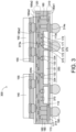
- FIG. 3 illustrates a diagram view of a cross-sectional view of a semiconductor device 300 according to another embodiment of the invention.
- the semiconductor device 300 may applied to a HBPoP, an InFO PoP, etc.
- the semiconductor device 300 includes a first layer structure 310, the second layer structure 120, at least one bridge die 330, at least one first SoC 140, at least one second SoC 150, at least one under-filler 155, at least one conductive pillar 160, at least one passive component 370, the first encapsulation body 180 and at least one conductive contact 190.
- the bridge die 330 is disposed between the first layer structure 310 and the second layer structure 120.
- the first SoC 140 and the second SoC 150 are disposed on the second layer structure 120.
- the first SoC 140 and the second SoC 150 are electrically connected through the bridge die 330.
- the semiconductor device 300 includes the features the same as or similar to that of the semiconductor device 100 except that, for example, the bridge die 330 of the semiconductor device 300 is different from the bridge die 130 of the semiconductor device 100. In comparison with the bridge die 130, the bridge die 330 may omit the conductive vias 132. The bridge die 330 may be electrically connected to the first layer structure 310 through the second layer structure 120 and the conductive pillar 160.
- the passive component 370 includes the substrate 171, at least one conductive contact 172 and at least one conductive contact 373, wherein the conductive contacts 373 is electrically connected to the conductive contact 172 and protrudes with respect to the conductive contact 172.
- the conductive contact 373 has a surface 373s.
- the bridge die 330 further includes at least one conductive contact 334, wherein the conductive contact 334 is formed on and electrically connected to the conductive contact 133, and protrudes with respect to the conductive contact 133.
- the conductive contact 334 has a surface 334s.
- the first encapsulation body 180 further has a second surface 180s2 opposite to the first surface 180s1.
- the surface 373s of the passive component 370, the surface 334s of the bridge die 330, the second surface 160s2 of the conductive pillar 160 and the second surface 180s2 of the first encapsulation body 180 are flush with each other.
- the semiconductor device 300 has a coplanar surface including at least two of a portion of the first encapsulation body 180, a portion of the passive component 370, a portion of the conductive pillar 160 and a portion of the bridge die 330.
- the first layer structure 310 includes at least one first conductive trace layer 111, at least one first conductive via layer 112, at least one first dielectric layer 113 and at least one first conductive contact 314.
- the first conductive contact 314 has a surface 314s, and the outermost first dielectric layer 113 has the surface 113s, wherein the surface 314s and the surface 113s are flush with each other.
- the first conductive contact 314 is, for example, a conductive bump, a conductive pad, etc.
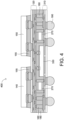
- FIG. 4 illustrates a diagram view of a cross-sectional view of a semiconductor device 400 according to another embodiment of the invention.
- the semiconductor device 400 may applied to a HBPoP, InFO PoP, etc.
- the semiconductor device 400 includes the first layer structure 310, the second layer structure 120, at least one bridge die 330, at least one first SoC 140, at least one second SoC 150, at least one under-filler 155, at least one conductive pillar 160, at least one passive component 270, the first encapsulation body 180 and at least one conductive contact 190.
- the bridge die 330 is disposed between the first layer structure 310 and the second layer structure 120.
- the first SoC 140 and the second SoC 150 are disposed on the second layer structure 120.
- the first SoC 140 and the second SoC 150 are electrically connected through the bridge die 330.
- the semiconductor device 400 includes the features the same as or similar to that of the semiconductor device 300 except that, for example, the passive component 170 of the semiconductor device 300 may be replaced by the passive component 270 of the semiconductor device 400.
- FIG. 5 illustrates a diagram view of a cross-sectional view of a semiconductor device 500 according to another embodiment of the invention.
- the semiconductor device 500 may applied to a HBPoP, InFO PoP, etc.
- the semiconductor device 500 includes the first layer structure 110, the second layer structure 120, at least one bridge die 130, at least one first SoC 140 and at least one second SoC 150, at least one conductive pillar 160, at least one passive component 170, the first encapsulation body 180, at least one conductive contact 190 and a second encapsulation body 580.
- the semiconductor device 500 includes the features the same as or similar to that of the semiconductor device 100 except that, for example, the semiconductor device 500 further include the second encapsulation body 580.
- the second encapsulation body 580 is formed on the second layer structure 120 and encapsulates the first SoC 140 and the second SoC 150 for protecting the first SoC 140 and the second SoC 150.
- the second encapsulation body 580 is, for example, molding compound.
- the molding compound may be formed of a molding material including, for example, a Novolac-based resin, an epoxy-based resin, a silicone-based resin, or another suitable encapsulant. Suitable fillers also may be included, such as powdered SiO2.
- the molding material may be applied using any of a number of molding techniques, such as compression molding, injection molding, or transfer molding.
- the semiconductor device 200 may further the second encapsulation body 580 encapsulating the first SoC 140 and the second SoC 150 for protecting the first SoC 140 and the second SoC 150.
- FIG. 6 illustrates a diagram view of a cross-sectional view of a semiconductor device 600 according to another embodiment of the invention.
- the semiconductor device 600 may applied to a HBPoP, InFO PoP, etc.
- the semiconductor device 600 includes the first layer structure 310, the second layer structure 120, at least one bridge die 330, at least one first SoC 140 and at least one second SoC 150, at least one conductive pillar 160, at least one passive component 370, the first encapsulation body 180, at least one conductive contact 190 and the second encapsulation body 580.
- the semiconductor device 600 includes the features the same as or similar to that of the semiconductor device 300 except that, for example, the semiconductor device 600 further include the second encapsulation body 580 encapsulating the first SoC 140 and the second SoC 150 for protecting the first SoC 140 and the second SoC 150.
- the semiconductor device 400 may further the second encapsulation body 580 encapsulating the first SoC 140 and the second SoC 150 for protecting the first SoC 140 and the second SoC 150.
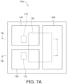
- FIG. 7A illustrates a diagram view of a top view of a semiconductor device 700 according to another embodiment of the invention
- FIG. 7B illustrates a diagram view of a cross-sectional view of the semiconductor device 700 of FIG. 7A in a direction 7B-7B'.
- the semiconductor device 700 may applied to a HB (High Bandwidth) PoP (Package on Package), Fan-out PoP, etc.
- HB High Bandwidth
- PoP Package on Package
- Fan-out PoP etc.
- the semiconductor device 700 includes the first layer structure 110, the second layer structure 120, at least one bridge die 130, at least one first SoC 140 and at least one second SoC 150, at least one conductive pillar 160, at least one passive component 170, the first encapsulation body 180, at least one conductive contact 190 and at least one memory die 640.
- the semiconductor device 700 includes the features the same as or similar to that of the semiconductor device 100 except that, for example, the semiconductor device 700 further include the memory die 640.
- the memory die 640 is disposed on the second layer structure 120.
- the first SoC 140, the second SoC 150 and the memory die 640 are electrically connected to each other through the bridge die 640.
- the first SoC 140, the second SoC 150 and the memory die 640 are not directly connected, but indirectly connected through the second layer structure 120 and the bridge die 130.
- the memory die 640 is, for example, DRAM, etc.
- the semiconductor device 700 may further include the second encapsulation body 580 of FIG. 5 encapsulating the first SoC 140, the second SoC 150 and the memory die 640 for protecting the first SoC 140, the second SoC 150 and the memory die 640.
- the semiconductor device 200 may further include the memory die 640 disposed on the second layer structure 120
- the semiconductor device 300 may further include the memory die 640 disposed on the second layer structure 120
- the semiconductor device 400 may further include the memory die 640 disposed on the second layer structure 120.
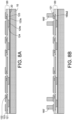
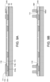
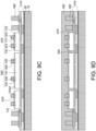
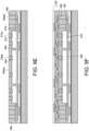
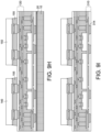
- FIGS. 8A to 8I illustrate schematic diagrams of a manufacturing method of the semiconductor device 100 of FIG. 1B .
- the second layer structure 120 (the first one) is formed on a first carrier 10 through a first release layer 20, wherein the second layer structure 120 includes at least one second conductive trace layer 121, at least one second conductive via layer 122, at least one second dielectric layer 123 and at least second conductive contact 124, wherein the adjacent two second conductive trace layers 121 are separated from one of the second dielectric layers 123, and the adjacent two second conductive trace layers 121 may be electrically connected by one of the second conductive via layers 122.
- the second conductive contact 124 has the surface 124s, and the outermost second dielectric layer 123 has the surface 123s, wherein the surface 124s and the surface 123s are flush with each other.
- the second conductive trace layer 121, the second conductive via layers 122 and the second conductive contact 124 may be formed by using, for example, electroplating, etc.
- the second dielectric layer 123 may be formed by using, for example, lithography, etc.
- At least one conductive pillar 160' is formed on the second layer structure 120 by using, for example, electroplating, etc. Furthermore, the conductive pillar 160' has the second surface 160s2, and the second surface 160s2 is formed on and electrically connected to the second conductive trace layer 121 or the second conductive via layer 122 of the second layer structure 120.
- At least one bridge die 130' and at least one passive component 170' are disposed on the second layer structure 120 by using, for example, a SMT (Surface mount technology).
- SMT Surface mount technology
- the bridge die 130' includes a silicon-based substrate 131', the plurality of the conductive vias 132 and a plurality of the conductive contacts 133.
- the silicon-based substrate 131' has the first surface 131 s1' and the second surface 131s2 opposite to the first surface 131s1', wherein the conductive via 132 is exposed from the second surface 131s2, but not exposed from the first surface 131s1'.
- Each conductive contact 133 is electrically to the corresponding conductive via 132.
- the conductive via 132 may be electrically connected to the second layer structure 120 through the conductive contacts 133.
- the passive component 170' includes a substrate 171' and a plurality of conductive contacts 172.
- the substrate 171' is, for example, a silicon-based substrate.
- the substrate 171' has a first surface 171s1' and the second surface 171s2 opposite to the first surface 171s1'.
- the conductive contacts 172 are formed on a side adjacent to the second surface 171s2 of the substrate 171.
- the conductive contacts 172 may be electrically connected to the second layer structure 120.
- the conductive contacts 171 may be electrically connected to the second conductive trace layer 121 or the second conductive via layer 122 of the second layer structure 120.
- conductive contact 172 is, for example, a solder ball, a conductive bump, a conductive pad, etc.
- a first encapsulation body material 180' encapsulating at least one bridge die 130', at least one passive component 170', at least one conductive pillar 160' is formed on the second layer structure 120 by using, for example, a compression molding, an injection molding or a transfer molding.
- a portion of the first encapsulation body material 180', a portion of the bridge die 130', a portion of the passive component 170' and a portion of the conductive pillar 160' are removed to form the first encapsulation body 180, the bridge die 130, the passive component 170 and the conductive pillar 160 respectively by using, for example, a CMP (Chemical-Mechanical Planarization).
- a CMP Chemical-Mechanical Planarization
- the first encapsulation body 180 has the first surface 180s1
- the bridge die 130 has the first surface 131s1
- the conductive via 132 has the first surface 132s1
- the passive component 170 has the first surface 171s1
- the conductive pillar 160 has the first surface 160s1 , wherein the first surface 180s1 , the first surface 131s1, the first surface 132s1, the first surface 171s1 and the first surface 160s1 are flush with each other.
- the first layer structure 110 (the second one) is formed on at least one bridge die 130, at least one conductive pillar 160, at least one passive component 170 and the first encapsulation body 180.
- the first layer structure 110 includes at least one first conductive trace layer 111, at least one first conductive via layer 112, at least one first dielectric layer 113 and at least first conductive contact 114, wherein the adjacent two first conductive trace layers 111 are separated from one of the first dielectric layers 113, and the adjacent two first conductive trace layers 111 may be electrically connected by one of the first conductive via layers 112.
- the first conductive contact 114 is electrically to the first conductive trace layer 111 or the first conductive via layer 112 of the first layer structure 110, and protrudes with respect to a surface 113s of the outermost first dielectric layers 113.
- the first conductive trace layer 111, the first conductive via layers 112 and the first conductive contact 114 may be formed by using, for example, electroplating, etc.
- the first dielectric layer 113 may be formed by using, for example, lithography, etc.
- At least one conductive contact 190 is formed on the first layer structure 110.
- the conductive contact 190 is formed on the first conductive contact 114 of the first layer structure 110.
- the first carrier 10 with the first release layer 20 of FIG. 8F are removed to expose the second dielectric layer 123 and the second conductive contact 124.
- FIG. 8H the structure of FIG. 8G is inverted to make the second dielectric layer 123 and the second conductive contact 124 face up.
- At least one first SoC 140 and at least one second SoC 150 are disposed on the second layer structure 120 by using, for example, a SMT.
- the first SoC 140 and the second SoC 150 are electrically connected to the second conductive contact 124 of the second layer structure 120.
- the under-filler 155 of FIG. 1B is formed between the first SoC 140 of FIG. 8I and the second layer structure 120 of FIG. 8I to encapsulate the contacts between the first SoC 140 of FIG. 8I and the second layer structure 120 of FIG. 8I
- another under-filler 155 of FIG. 1B is formed between the second SoC 150 of FIG. 8I and the second layer structure 120 of FIG. 8I to encapsulate the contacts between the second SoC 150 of FIG. 8I and the second layer structure 120 of FIG. 8I . So far, the semiconductor device 100 is completed.
- the semiconductor device 200 may be formed by using the manufacturing method the same as or similar to that of the semiconductor device 100, and the similarities will not be repeated here.
- FIGS. 9A to 9I illustrate schematic diagrams of a manufacturing method of the semiconductor device 300 of FIG. 3 .
- the first layer structure 310 (the first one) is formed on the first carrier 10 through the first release layer 20.
- the first layer structure 310 includes at least one first conductive trace layer 111, at least one first conductive via layer 112, at least one first dielectric layer 113 and at least first conductive contact 314, wherein the adjacent two first conductive trace layers 111 are separated from one of the first dielectric layers 113, and the adjacent two first conductive trace layers 111 may be electrically connected by one of the first conductive via layers 112.
- the first conductive contact 314 is electrically to the first conductive trace layer 111 or the first conductive via layer 112 of the first layer structure 310.
- the first conductive contact 314 has the surface 314s, and the outermost first dielectric layer 113 has the surface 113s, wherein the surface 314s and the surface 113s are flush with each other.
- the first conductive trace layer 111, the first conductive via layers 112 and the first conductive contact 314 may be formed by using, for example, electroplating, etc.
- the first dielectric layer 113 may be formed by using, for example, lithography, etc.
- At least one conductive pillar 160' is formed on the first layer structure 310 by using, for example, electroplating, etc. Furthermore, the conductive pillar 160' has the first surface 160s1, and the first surface 160s1 is formed on and electrically connected to the first conductive trace layer 111 or the first conductive via layer 112 of the first layer structure 310.
- At least one bridge die 330' and at least one passive component 370' are disposed on the first layer structure 310 by using, for example, a SMT.
- the passive component 370 includes the substrate 171, at least one conductive contact 172 and at least one conductive contact 373', wherein the conductive contacts 373' is electrically connected to the conductive contact 172 and protrudes with respect to the conductive contact 172.
- the bridge die 330' includes the silicon-based substrate 131, a plurality of the conductive contacts 133 and a plurality of conductive contacts 334'.
- the conductive contact 334' is formed on and electrically connected to the conductive contact 133, and protrudes with respect to the conductive contact 133.
- the first encapsulation body material 180' encapsulating at least one bridge die 330', at least one passive component 370', at least one conductive pillar 160' is formed on the first layer structure 310 by using, for example, a compression molding, an injection molding or a transfer molding.
- a portion of the first encapsulation body material 180', a portion of the bridge die 330', a portion of the passive component 370' and a portion of the conductive pillar 160' are removed to form the first encapsulation body 180, the bridge die 330, the passive component 370 and the conductive pillar 160 respectively by using, for example, a CMP.
- a coplanar surface including at least two of a portion of the first encapsulation body 180, a portion of the passive component 370, a portion of the conductive pillar 160 and a portion of the bridge die 330 is formed.
- the first encapsulation body 180 has the second surface 180s2
- the conductive contact 334 of the bridge die 330 has the surface 334s
- the conductive contact 373 of the passive component 370 has the surface 373s
- the conductive pillar 160 has the second surface 160s2, wherein the surface 373s of the passive component 370, the surface 334s of the bridge die 330, the second surface 160s2 of the conductive pillar 160 and the second surface 180s2 of the first encapsulation body 180 are flush with each other.
- the second layer structure 120 (the second one) is formed on the bridge die 330, the conductive pillar 160, the first encapsulation body 180 and the passive component 370.
- At least one first SoC 140 and at least one second SoC 150 are disposed on the second layer structure 120 by using, for example, a SMT.
- the first SoC 140 and the second SoC 150 are electrically connected to the second conductive contact 124 of the second layer structure 120.
- the under-filler 155 is formed between the first SoC 140 and the second layer structure 120 to encapsulate the contacts between the first SoC 140 and the second layer structure 120, and another under-filler 155 is formed between the second SoC 150 and the second layer structure 120 to encapsulate the contacts between the second SoC 150 and the second layer structure 120.
- the first carrier 10 with the first release layer 20 of FIG. 9H are removed to expose the conductive contact 314 of the first layer structure 310.
- At least one conductive contact 190 is formed on the first layer structure 310.
- the conductive contact 190 is formed on the exposed first conductive contact 314 of the first layer structure 310. So far, the semiconductor device 300 is completed.
- the semiconductor device 400 may be formed by using the manufacturing method the same as or similar to that of the semiconductor device 300, and the similarities will not be repeated here.
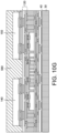
- FIGS. 10A to 10H illustrate schematic diagrams of a manufacturing method of the semiconductor device 500 of FIG. 5 .
- the structure of FIG. 8E is formed, and then the first layer structure 110 is formed on at least one bridge die 130, at least one conductive pillar 160, at least one passive component 170 and the first encapsulation body 180.
- a second carrier 30 is disposed on the first layer structure 110 through a second release layer 40, wherein a protrusion of the first conductive contact 114 of the first layer structure 110 is embedded in the release layer 40.
- the second carrier 10 with the second release layer 20 of FIG. 10B are removed to expose the second dielectric layer 123 and the second conductive contact 124.
- FIG. 10D the structure of FIG. 10C is inverted to make the second conductive contact 124 face up.
- At least one first SoC 140 and at least one second SoC 150 are disposed on the second layer structure 120 by using, for example, a SMT.
- the first SoC 140 and the second SoC 150 are electrically connected to the second conductive contact 124 of the second layer structure 120.
- the under-filler 155 is formed between the first SoC 140 and the second layer structure 120 to encapsulate the contacts between the first SoC 140 and the second layer structure 120, and another under-filler 155 is formed between the second SoC 150 and the second layer structure 120 to encapsulate the contacts between the second SoC 150 and the second layer structure 120.
- the second encapsulation body 580 encapsulating the first SoC 140 and the second SoC 150 is formed on the second layer structure 120.
- the second carrier 30 with the second release layer 40 of FIG. 10G are removed to expose the first conductive contact 114 of the first layer structure 110.
- At least one conductive contact 190 is formed on the first layer structure 110 of FIG. 10H .
- the conductive contact 190 is formed on the first conductive contact 114 of the first layer structure 110 of FIG. 10H . So far, the semiconductor device 500 of FIG. 5 is completed.
- the semiconductor device 600 may be formed by using the manufacturing method the same as or similar to that of the semiconductor device 500, and the similarities will not be repeated here.
- the semiconductor device 700 may be formed by using the manufacturing method the same as or similar to that of the semiconductor device 100, and the similarities will not be repeated here.
Landscapes
- Semiconductor Integrated Circuits (AREA)
- Internal Circuitry In Semiconductor Integrated Circuit Devices (AREA)
- Physics & Mathematics (AREA)
- Geometry (AREA)
- Metal-Oxide And Bipolar Metal-Oxide Semiconductor Integrated Circuits (AREA)
Applications Claiming Priority (2)
| Application Number | Priority Date | Filing Date | Title |
|---|---|---|---|
| US202263345058P | 2022-05-24 | 2022-05-24 | |
| US18/191,092 US12581971B2 (en) | 2022-05-24 | 2023-03-28 | Semiconductor device with bridge die electrically connecting two chips and manufacturing method thereof |
Publications (2)
| Publication Number | Publication Date |
|---|---|
| EP4283671A2 true EP4283671A2 (de) | 2023-11-29 |
| EP4283671A3 EP4283671A3 (de) | 2024-04-03 |
Family
ID=86226614
Family Applications (1)
| Application Number | Title | Priority Date | Filing Date |
|---|---|---|---|
| EP23170173.1A Pending EP4283671A3 (de) | 2022-05-24 | 2023-04-26 | Halbleiterbauelement und herstellungsverfahren dafür |
Country Status (3)
| Country | Link |
|---|---|
| US (1) | US12581971B2 (de) |
| EP (1) | EP4283671A3 (de) |
| TW (1) | TWI845316B (de) |
Cited By (1)
| Publication number | Priority date | Publication date | Assignee | Title |
|---|---|---|---|---|
| WO2025117170A1 (en) * | 2023-11-30 | 2025-06-05 | Qualcomm Incorporated | Bridge die in substrate core layer |
Family Cites Families (10)
| Publication number | Priority date | Publication date | Assignee | Title |
|---|---|---|---|---|
| KR20130124858A (ko) | 2012-05-07 | 2013-11-15 | 삼성전자주식회사 | 반도체 패키지 |
| US10497674B2 (en) | 2016-01-27 | 2019-12-03 | Amkor Technology, Inc. | Semiconductor package and fabricating method thereof |
| US10943869B2 (en) | 2017-06-09 | 2021-03-09 | Apple Inc. | High density interconnection using fanout interposer chiplet |
| US10763239B2 (en) * | 2017-10-27 | 2020-09-01 | Taiwan Semiconductor Manufacturing Co., Ltd. | Multi-chip wafer level packages and methods of forming the same |
| US11133256B2 (en) | 2019-06-20 | 2021-09-28 | Intel Corporation | Embedded bridge substrate having an integral device |
| US20210005542A1 (en) | 2019-07-03 | 2021-01-07 | Intel Corporation | Nested interposer package for ic chips |
| TW202111907A (zh) | 2019-09-05 | 2021-03-16 | 力成科技股份有限公司 | 以矽中介層作為互連橋的封裝晶片結構 |
| US11164817B2 (en) | 2019-11-01 | 2021-11-02 | International Business Machines Corporation | Multi-chip package structures with discrete redistribution layers |
| KR102937985B1 (ko) * | 2021-03-26 | 2026-03-12 | 삼성전자주식회사 | 반도체 패키지 |
| US20230050400A1 (en) | 2021-08-13 | 2023-02-16 | Mediatek Inc. | Semiconductor package with reduced connection length |
-
2023
- 2023-03-28 US US18/191,092 patent/US12581971B2/en active Active
- 2023-04-26 EP EP23170173.1A patent/EP4283671A3/de active Pending
- 2023-05-22 TW TW112118916A patent/TWI845316B/zh active
Cited By (1)
| Publication number | Priority date | Publication date | Assignee | Title |
|---|---|---|---|---|
| WO2025117170A1 (en) * | 2023-11-30 | 2025-06-05 | Qualcomm Incorporated | Bridge die in substrate core layer |
Also Published As
| Publication number | Publication date |
|---|---|
| US12581971B2 (en) | 2026-03-17 |
| US20230387025A1 (en) | 2023-11-30 |
| TW202347700A (zh) | 2023-12-01 |
| TWI845316B (zh) | 2024-06-11 |
| EP4283671A3 (de) | 2024-04-03 |
Similar Documents
| Publication | Publication Date | Title |
|---|---|---|
| US11837552B2 (en) | Semiconductor package with layer structures, antenna layer and electronic component | |
| US12040304B2 (en) | Semiconductor package and method of fabricating the same | |
| US12255182B2 (en) | Electronic package and manufacturing method thereof | |
| US10186488B2 (en) | Manufacturing method of semiconductor package and manufacturing method of semiconductor device | |
| US11824020B2 (en) | Semiconductor package structure including antenna | |
| TWI818458B (zh) | 電子封裝件及其製法 | |
| US12494460B2 (en) | Electronic package and manufacturing method thereof | |
| US11114415B2 (en) | Semiconductor device with a layered protection mechanism and associated systems, devices, and methods | |
| WO2005122257A1 (ja) | コンデンサを内蔵した半導体装置及びその製造方法 | |
| CN113380772B (zh) | 一种芯片封装结构及其封装方法 | |
| EP4283671A2 (de) | Halbleiterbauelement und herstellungsverfahren dafür | |
| CN114121833A (zh) | 电子封装件及其制法与电子结构 | |
| US12557704B2 (en) | Semiconductor device | |
| US10269718B2 (en) | Rectangular semiconductor package and a method of manufacturing the same | |
| US20250293224A1 (en) | Electronic package and manufacturing method thereof | |
| US12368104B2 (en) | Electronic package | |
| TWI815639B (zh) | 電子封裝件及其製法 | |
| CN117116905A (zh) | 半导体装置及其制造方法 | |
| US20260005199A1 (en) | Electronic package and manufacturing method thereof | |
| US20250336739A1 (en) | Electronic package and manufacturing method thereof | |
| US20250140635A1 (en) | Electronic package and manufacturing method thereof |
Legal Events
| Date | Code | Title | Description |
|---|---|---|---|
| PUAI | Public reference made under article 153(3) epc to a published international application that has entered the european phase |
Free format text: ORIGINAL CODE: 0009012 |
|
| STAA | Information on the status of an ep patent application or granted ep patent |
Free format text: STATUS: THE APPLICATION HAS BEEN PUBLISHED |
|
| AK | Designated contracting states |
Kind code of ref document: A2 Designated state(s): AL AT BE BG CH CY CZ DE DK EE ES FI FR GB GR HR HU IE IS IT LI LT LU LV MC ME MK MT NL NO PL PT RO RS SE SI SK SM TR |
|
| RIC1 | Information provided on ipc code assigned before grant |
Ipc: H01L 21/60 20060101ALI20231110BHEP Ipc: H01L 25/18 20230101ALI20231110BHEP Ipc: H01L 25/065 20230101AFI20231110BHEP |
|
| PUAL | Search report despatched |
Free format text: ORIGINAL CODE: 0009013 |
|
| AK | Designated contracting states |
Kind code of ref document: A3 Designated state(s): AL AT BE BG CH CY CZ DE DK EE ES FI FR GB GR HR HU IE IS IT LI LT LU LV MC ME MK MT NL NO PL PT RO RS SE SI SK SM TR |
|
| RIC1 | Information provided on ipc code assigned before grant |
Ipc: H01L 25/16 20230101ALI20240226BHEP Ipc: H01L 21/60 20060101ALI20240226BHEP Ipc: H01L 25/18 20230101ALI20240226BHEP Ipc: H01L 25/065 20230101AFI20240226BHEP |
|
| STAA | Information on the status of an ep patent application or granted ep patent |
Free format text: STATUS: REQUEST FOR EXAMINATION WAS MADE |
|
| 17P | Request for examination filed |
Effective date: 20240911 |
|
| RBV | Designated contracting states (corrected) |
Designated state(s): AL AT BE BG CH CY CZ DE DK EE ES FI FR GB GR HR HU IE IS IT LI LT LU LV MC ME MK MT NL NO PL PT RO RS SE SI SK SM TR |