EP4280267A2 - Integrated circuit electrostatic discharge bus structure and related method - Google Patents
Integrated circuit electrostatic discharge bus structure and related method Download PDFInfo
- Publication number
- EP4280267A2 EP4280267A2 EP23202083.4A EP23202083A EP4280267A2 EP 4280267 A2 EP4280267 A2 EP 4280267A2 EP 23202083 A EP23202083 A EP 23202083A EP 4280267 A2 EP4280267 A2 EP 4280267A2
- Authority
- EP
- European Patent Office
- Prior art keywords
- pad
- esd
- pad groups
- integrated circuit
- groups
- Prior art date
- Legal status (The legal status is an assumption and is not a legal conclusion. Google has not performed a legal analysis and makes no representation as to the accuracy of the status listed.)
- Granted
Links
Images


Classifications
-
- H—ELECTRICITY
- H10—SEMICONDUCTOR DEVICES; ELECTRIC SOLID-STATE DEVICES NOT OTHERWISE PROVIDED FOR
- H10D—INORGANIC ELECTRIC SEMICONDUCTOR DEVICES
- H10D89/00—Aspects of integrated devices not covered by groups H10D84/00 - H10D88/00
- H10D89/60—Integrated devices comprising arrangements for electrical or thermal protection, e.g. protection circuits against electrostatic discharge [ESD]
- H10D89/601—Integrated devices comprising arrangements for electrical or thermal protection, e.g. protection circuits against electrostatic discharge [ESD] for devices having insulated gate electrodes, e.g. for IGFETs or IGBTs
- H10D89/921—Integrated devices comprising arrangements for electrical or thermal protection, e.g. protection circuits against electrostatic discharge [ESD] for devices having insulated gate electrodes, e.g. for IGFETs or IGBTs characterised by the configuration of the interconnections connecting the protective arrangements, e.g. ESD buses
-
- H—ELECTRICITY
- H10—SEMICONDUCTOR DEVICES; ELECTRIC SOLID-STATE DEVICES NOT OTHERWISE PROVIDED FOR
- H10W—GENERIC PACKAGES, INTERCONNECTIONS, CONNECTORS OR OTHER CONSTRUCTIONAL DETAILS OF DEVICES COVERED BY CLASS H10
- H10W72/00—Interconnections or connectors in packages
-
- H—ELECTRICITY
- H10—SEMICONDUCTOR DEVICES; ELECTRIC SOLID-STATE DEVICES NOT OTHERWISE PROVIDED FOR
- H10D—INORGANIC ELECTRIC SEMICONDUCTOR DEVICES
- H10D89/00—Aspects of integrated devices not covered by groups H10D84/00 - H10D88/00
- H10D89/60—Integrated devices comprising arrangements for electrical or thermal protection, e.g. protection circuits against electrostatic discharge [ESD]
-
- H—ELECTRICITY
- H10—SEMICONDUCTOR DEVICES; ELECTRIC SOLID-STATE DEVICES NOT OTHERWISE PROVIDED FOR
- H10W—GENERIC PACKAGES, INTERCONNECTIONS, CONNECTORS OR OTHER CONSTRUCTIONAL DETAILS OF DEVICES COVERED BY CLASS H10
- H10W72/00—Interconnections or connectors in packages
- H10W72/50—Bond wires
-
- H—ELECTRICITY
- H10—SEMICONDUCTOR DEVICES; ELECTRIC SOLID-STATE DEVICES NOT OTHERWISE PROVIDED FOR
- H10W—GENERIC PACKAGES, INTERCONNECTIONS, CONNECTORS OR OTHER CONSTRUCTIONAL DETAILS OF DEVICES COVERED BY CLASS H10
- H10W72/00—Interconnections or connectors in packages
- H10W72/90—Bond pads, in general
-
- H—ELECTRICITY
- H10—SEMICONDUCTOR DEVICES; ELECTRIC SOLID-STATE DEVICES NOT OTHERWISE PROVIDED FOR
- H10W—GENERIC PACKAGES, INTERCONNECTIONS, CONNECTORS OR OTHER CONSTRUCTIONAL DETAILS OF DEVICES COVERED BY CLASS H10
- H10W72/00—Interconnections or connectors in packages
- H10W72/071—Connecting or disconnecting
- H10W72/075—Connecting or disconnecting of bond wires
- H10W72/07531—Techniques
-
- H—ELECTRICITY
- H10—SEMICONDUCTOR DEVICES; ELECTRIC SOLID-STATE DEVICES NOT OTHERWISE PROVIDED FOR
- H10W—GENERIC PACKAGES, INTERCONNECTIONS, CONNECTORS OR OTHER CONSTRUCTIONAL DETAILS OF DEVICES COVERED BY CLASS H10
- H10W72/00—Interconnections or connectors in packages
- H10W72/071—Connecting or disconnecting
- H10W72/075—Connecting or disconnecting of bond wires
- H10W72/07551—Connecting or disconnecting of bond wires characterised by changes in properties of the bond wires during the connecting
- H10W72/07554—Connecting or disconnecting of bond wires characterised by changes in properties of the bond wires during the connecting changes in dispositions
-
- H—ELECTRICITY
- H10—SEMICONDUCTOR DEVICES; ELECTRIC SOLID-STATE DEVICES NOT OTHERWISE PROVIDED FOR
- H10W—GENERIC PACKAGES, INTERCONNECTIONS, CONNECTORS OR OTHER CONSTRUCTIONAL DETAILS OF DEVICES COVERED BY CLASS H10
- H10W72/00—Interconnections or connectors in packages
- H10W72/50—Bond wires
- H10W72/541—Dispositions of bond wires
- H10W72/5453—Dispositions of bond wires connecting between multiple bond pads on a chip, e.g. daisy chain
-
- H—ELECTRICITY
- H10—SEMICONDUCTOR DEVICES; ELECTRIC SOLID-STATE DEVICES NOT OTHERWISE PROVIDED FOR
- H10W—GENERIC PACKAGES, INTERCONNECTIONS, CONNECTORS OR OTHER CONSTRUCTIONAL DETAILS OF DEVICES COVERED BY CLASS H10
- H10W72/00—Interconnections or connectors in packages
- H10W72/50—Bond wires
- H10W72/59—Bond pads specially adapted therefor
-
- H—ELECTRICITY
- H10—SEMICONDUCTOR DEVICES; ELECTRIC SOLID-STATE DEVICES NOT OTHERWISE PROVIDED FOR
- H10W—GENERIC PACKAGES, INTERCONNECTIONS, CONNECTORS OR OTHER CONSTRUCTIONAL DETAILS OF DEVICES COVERED BY CLASS H10
- H10W72/00—Interconnections or connectors in packages
- H10W72/90—Bond pads, in general
- H10W72/941—Dispositions of bond pads
- H10W72/944—Dispositions of multiple bond pads
- H10W72/9445—Top-view layouts, e.g. mirror arrays
Definitions
- the present invention relates to an integrated circuit structure and related method, and more particularly, to an integrated circuit electrostatic discharge bus structure and related method.
- I/O pads 12 are placed around a circuit area 10 inside a plurality of chip edges 13 based on particular sequence and position, wherein the placement of the I/O pads 12 is adjustable within a specific range.
- ESD electrostatic discharge
- the filler cells F1 and F2 take a portion of the circuit area 10 to be wasteful to the integrated circuit ESD bus structure 1. Further, under the strict requirement of the integrated circuit ESD bus structure 1 having a rectangular shape, it causes the lack of flexibility for internal circuit layout design.
- circuit area 10 when there are circuits with irregular shapes and different areas, the circuit area 10 must be increased in order to contain the circuits with irregular shapes and different areas, which increases production cost.
- an integrated circuit electrostatic discharge (ESD) structure includes a circuit area; a plurality of electrostatic discharge buses; a plurality of pad groups adjacent and connected to the plurality of ESD buses; a common ESD bus; and a plurality of bonding wires configured to connect the plurality of pad groups to the common ESD bus.
- an integrated circuit electrostatic discharge (ESD) structure includes a circuit area; a plurality of electrostatic discharge (ESD) buses; a plurality of pad groups; and a plurality of bonding wires configured to connect one to another of the plurality of pad groups.
- a method of integrated circuit ESD bus structure includes forming a circuit area; forming a plurality of pad groups corresponding to a plurality of discontinuous boundaries of the circuit area; forming a common ESD bus; and connecting a plurality of pads corresponding to the plurality of pad groups to the common ESD bus by a plurality of bonding wires across one of the plurality of chip edges.
- a method of integrated circuit ESD bus structure includes forming a circuit area, forming a plurality of pad groups corresponding to a plurality of discontinuous boundaries of the circuit area; and connecting one of the plurality of pad groups to another of the plurality of pad groups by one of a plurality of bonding wires across the circuit area.
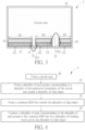
- FIG. 2 is a schematic diagram of an integrated circuit electrostatic discharge (ESD) structure 2 according to an embodiment of the present invention.
- the integrated circuit ESD bus structure 2 includes a circuit area 20, a plurality of ESD buses E1, E2 and E3, a plurality of pad groups G1, G2 and G3, a common ESD bus 24, and a plurality of bonding wires 25.
- the circuit area 20 is formed by a plurality of chip edges 23; for example, the four chip edges 23 forms a rectangular area configured to contain the circuit area 20.
- the circuit area 20 includes a plurality of discontinuous boundaries B 1, B2 and B3.
- the plurality of ESD buses E1, E2 and E3 is formed inside the chip edges 23, corresponding and adjacent to the plurality of discontinuous boundaries B 1, B2, and B3.
- the plurality of pad groups G1, G2 and G3 is formed inside the chip edges 23, adjacent and connected to the plurality of ESD buses E1, E2 and E3.
- the common ESD bus 24 is formed outside the chip edges 23, which is not limited.
- the common ESD bus 24 may not be formed in one piece, and include a plurality of discontinuous ESD bus groups.
- the plurality of bonding wires 25 is formed across the chip edges 23, and configured to connect the plurality of pad groups B 1, B2 and B3 to the common ESD bus 24.
- the common ESD bus 24 is parallel to the plurality of ESD buses E1, E2 and E3 and the plurality of pad groups G1, G2 and G3.
- Each of the plurality of pad groups G1, G2 and G3 includes at least one pad 22, wherein the pad 22 is an input/output pad connected to a ground or a system low voltage.
- At least one of the plurality of bonding wires 25 is configured to connect the at least one pad 22 to the common ESD bus 24.
- multiple bonding wires 25 may be configured to connect multiple pads 22 of the pad group G1 to the common ESD bus 24, which provides multiple connections to enhance conductivity between the pad group G1 and the common ESD bus 24 to improve ESD protection.
- the discontinuous ESD buses E1, E2 and E3 may be connected together by connecting the pads 22 of the pad groups G1, G2 and G3 to the common ESD bus 24 through the bonding wires 25, which equivalently forms a continuous ESD bus for the integrated circuit ESD bus structure 2.
- the present invention may get rid of the filler cells of the prior art.
- spaces between the discontinuous ESD buses E1 and E2 (or, E2 and E3) may be configured with circuit elements to make full use of the integrated circuit ESD bus structure 2.
- the ESD bus 11 and the filler cells F1 and F2 shown in FIG. 1 are replaced by saved areas SA1 and SA2 in FIG. 2 .
- the saved area SA1 is adjacent to the ESD buses E1 and E2 and the pads 22 of the pad groups G1 and G2.
- the saved area SA2 is adjacent to the ESD buses E2 and E3 and the pads 22 of the pad groups G2 and G3.
- the common ESD bus 24 is formed inside the chip edges 23, and adjacent to the plurality of pad groups G1, G2 and G3 and the saved areas SA1 and SA2.
- FIG. 3 is a schematic diagram of an integrated circuit ESD bus structure 3 according to an embodiment of the present invention.
- the integrated circuit ESD bus structure 3 includes a circuit area 30, a plurality of ESD buses E1, E2 and E3, a plurality of pad groups G1, G2 and G3, and a plurality of bonding wires 35.
- the circuit area 30 is formed by a plurality of chip edges 33; for example, the four chip edges 33 form a rectangular area to contain the circuit area 30.
- the circuit area 30 includes a plurality of discontinuous boundaries B 1, B2 and B3.
- the plurality of ESD buses E1, E2 and E3 is formed inside the chip edges 33, corresponding and adjacent to the plurality of discontinuous boundaries B1, B2, and B3.
- the plurality of discontinuous ESD buses E1, E2 and E3 is formed inside the chip edges 33, and adjacent to the plurality of discontinuous boundaries B 1, B2, and B3.
- the plurality of pad groups G1, G2, and G3 is formed inside the chip edges 33, adjacent and connected to the plurality of ESD buses E1, E2 and E3.
- the plurality of bonding wires 35 is formed across the circuit area 30, and configured to connect the plurality of pad groups G1, G2, and G3 from one group to another group, e.g., one bonding wire 35 may connect the pad group G1 to the pad group G2, and another bonding wire 35 may connect the pad group G2 to the pad group G3.
- Each of the plurality of pad groups G1, G2 and G3 includes a plurality of pads 32, wherein the pad 32 is an input/output pad connected to a ground or a system low voltage.
- the plurality of bonding wires 35 is configured to connect the pads 32 of one group to another group.
- Each of the plurality of pad groups G1, G2 and G3 comprises a connecting pad (e.g., a right most pad of the pad group G1, left and right most pads of the pad group G2, and a left most pad of the pad group G3), and the plurality of bonding wires 35 are configured to connect the connecting pad of one of the plurality of pad groups to the connecting pad of another of the plurality of pad groups.
- one of the bonding wires 35 is configured to connect the right most pad 32 of the pad group G1 to the left most pad 32 of the pad group G2, and one of the bonding wires 35 is configured to connect the right most pad 32 of the pad group G2 to the left most pad 32 of the pad group G3, which is not limited.
- the discontinuous ESD buses E1, E2 and E3 may be connected together by connecting the pads 32 of the pad groups G1, G2 and G3 from one group to another group, which equivalently forms a continuous ESD bus for the integrated circuit ESD bus structure 3.
- the present invention may get rid of the filler cells of the prior art.
- spaces between the discontinuous ESD buses E1 and E2 may be configured with circuit elements to make full use of the integrated circuit ESD bus structure 3.
- the ESD bus 11 and the filler cells F1 and F2 shown in FIG. 1 are replaced by saved areas SA1 and SA2 in FIG. 2 , and thus the circuit area 20 may contain the circuits with irregular shapes and different areas without increasing its area, which saves production cost.
- FIG. 4 is a flowchart of an integrated circuit ESD bus structure process 4 according to an embodiment of the present invention.
- Step 40 a circuit area is formed; in step 41, a plurality of pad groups corresponding to a plurality of discontinuous boundaries of a circuit area inside a plurality of chip edges is formed; in step 42, a common ESD bus outside the plurality of chip edges is formed; and in step 43, a plurality of pads corresponding to the plurality of pad groups is connected to the common ESD bus by a plurality of bonding wires across the plurality of chip edges.
- a continuous ESD bus may be equivalently formed and the filler cells of the prior art may be omitted.
- FIG. 5 is a flowchart of an integrated circuit ESD bus structure process 5 according to an embodiment of the present invention.
- Step 50 a circuit area is formed; in step 51, a plurality of pad groups corresponding to a plurality of discontinuous boundaries of a circuit area inside a plurality of chip edges is formed; and in step 52, one and another of the plurality of pad groups are connected together by a plurality of bonding wires across the circuit area inside the plurality of chip edges.
- a continuous ESD bus may be equivalently formed and the filler cells of the prior art may be omitted.
- the present invention utilizes bonding wires to connect a plurality of pads of a plurality of pad groups, so as to equivalently form a continuous ESD bus.
- the present invention may get rid of the filler cells of the prior art.
- spaces between the discontinuous ESD buses may be configured with circuit elements to make full use of the integrated circuit ESD bus structure.
Landscapes
- Semiconductor Integrated Circuits (AREA)
- Wire Bonding (AREA)
- Internal Circuitry In Semiconductor Integrated Circuit Devices (AREA)
- Physics & Mathematics (AREA)
- Geometry (AREA)
- Engineering & Computer Science (AREA)
- Power Engineering (AREA)
- Design And Manufacture Of Integrated Circuits (AREA)
Abstract
Description
- The present invention relates to an integrated circuit structure and related method, and more particularly, to an integrated circuit electrostatic discharge bus structure and related method.
- For an integrated circuit electrostatic discharge (hereinafter abbreviated ESD) structure 1 as shown in
FIG. 1 , I/O (input/output)pads 12 are placed around acircuit area 10 inside a plurality ofchip edges 13 based on particular sequence and position, wherein the placement of the I/O pads 12 is adjustable within a specific range. - In general, it is commonly to place filler cells F1 and F2 at empty spaces between the I/
O pads 12, and connect the filler cells F1 and F2 to an electrostatic discharge (ESD) bus 11 (e.g., a layout trace connected to a ground or a system voltage), which makes each portion of thecircuit area 10 and the filler cells F1 and F2 are connected to the continuous ESD bus to provide ESD protection to the integrated circuit ESD bus structure 1. - However, the filler cells F1 and F2 take a portion of the
circuit area 10 to be wasteful to the integrated circuit ESD bus structure 1. Further, under the strict requirement of the integrated circuit ESD bus structure 1 having a rectangular shape, it causes the lack of flexibility for internal circuit layout design. - Further, when there are circuits with irregular shapes and different areas, the
circuit area 10 must be increased in order to contain the circuits with irregular shapes and different areas, which increases production cost. - Accordingly, it is desirable to provide an integrated circuit ESD bus structure and related method to make full use of the circuit area.
- It is therefore an objective of the present invention to provide an integrated circuit electrostatic discharge bus structure and related method.
- To achieve the above technical object, according to the present invention, an integrated circuit electrostatic discharge (ESD) structure is provided, and includes a circuit area; a plurality of electrostatic discharge buses; a plurality of pad groups adjacent and connected to the plurality of ESD buses; a common ESD bus; and a plurality of bonding wires configured to connect the plurality of pad groups to the common ESD bus.
- To achieve the above technical object, according to the present invention, an integrated circuit electrostatic discharge (ESD) structure is provided, and includes a circuit area; a plurality of electrostatic discharge (ESD) buses; a plurality of pad groups; and a plurality of bonding wires configured to connect one to another of the plurality of pad groups.
- To achieve the above technical object, according to the present invention, a method of integrated circuit ESD bus structure is provided, and includes forming a circuit area; forming a plurality of pad groups corresponding to a plurality of discontinuous boundaries of the circuit area; forming a common ESD bus; and connecting a plurality of pads corresponding to the plurality of pad groups to the common ESD bus by a plurality of bonding wires across one of the plurality of chip edges.
- To achieve the above technical object, according to the present invention, a method of integrated circuit ESD bus structure is provided, and includes forming a circuit area, forming a plurality of pad groups corresponding to a plurality of discontinuous boundaries of the circuit area; and connecting one of the plurality of pad groups to another of the plurality of pad groups by one of a plurality of bonding wires across the circuit area.
- These and other objectives of the present invention will no doubt become obvious to those of ordinary skill in the art after reading the following detailed description of the preferred embodiment that is illustrated in the various figures and drawings.
-
-
FIG. 1 is a schematic diagram of an integrated circuit ESD bus structure according to the prior art. -
FIG. 2 is a schematic diagram of an integrated circuit ESD bus structure according to an embodiment of the present invention. -
FIG. 3 is a schematic diagram of an integrated circuit ESD bus structure according to an embodiment of the present invention. -
FIG. 4 is a flowchart of an integrated circuit packaging process according to an embodiment of the present invention. -
FIG. 5 is a flowchart of an integrated circuit packaging process according to an embodiment of the present invention. -
FIG. 2 is a schematic diagram of an integrated circuit electrostatic discharge (ESD) structure 2 according to an embodiment of the present invention. The integrated circuit ESD bus structure 2 includes acircuit area 20, a plurality of ESD buses E1, E2 and E3, a plurality of pad groups G1, G2 and G3, acommon ESD bus 24, and a plurality ofbonding wires 25. - The
circuit area 20 is formed by a plurality ofchip edges 23; for example, the fourchip edges 23 forms a rectangular area configured to contain thecircuit area 20. Thecircuit area 20 includes a plurality of discontinuous boundaries B 1, B2 and B3. The plurality of ESD buses E1, E2 and E3 is formed inside thechip edges 23, corresponding and adjacent to the plurality of discontinuous boundaries B 1, B2, and B3. - The plurality of pad groups G1, G2 and G3 is formed inside the
chip edges 23, adjacent and connected to the plurality of ESD buses E1, E2 and E3. Thecommon ESD bus 24 is formed outside thechip edges 23, which is not limited. Thecommon ESD bus 24 may not be formed in one piece, and include a plurality of discontinuous ESD bus groups. The plurality ofbonding wires 25 is formed across thechip edges 23, and configured to connect the plurality of pad groups B 1, B2 and B3 to thecommon ESD bus 24. In one embodiment, thecommon ESD bus 24 is parallel to the plurality of ESD buses E1, E2 and E3 and the plurality of pad groups G1, G2 and G3. - Each of the plurality of pad groups G1, G2 and G3 includes at least one
pad 22, wherein thepad 22 is an input/output pad connected to a ground or a system low voltage. At least one of the plurality ofbonding wires 25 is configured to connect the at least onepad 22 to thecommon ESD bus 24. In one embodiment,multiple bonding wires 25 may be configured to connectmultiple pads 22 of the pad group G1 to thecommon ESD bus 24, which provides multiple connections to enhance conductivity between the pad group G1 and thecommon ESD bus 24 to improve ESD protection. - In such a structure, the discontinuous ESD buses E1, E2 and E3 may be connected together by connecting the
pads 22 of the pad groups G1, G2 and G3 to thecommon ESD bus 24 through thebonding wires 25, which equivalently forms a continuous ESD bus for the integrated circuit ESD bus structure 2. As a result, the present invention may get rid of the filler cells of the prior art. In addition, spaces between the discontinuous ESD buses E1 and E2 (or, E2 and E3) may be configured with circuit elements to make full use of the integrated circuit ESD bus structure 2. - For example, the
ESD bus 11 and the filler cells F1 and F2 shown inFIG. 1 are replaced by saved areas SA1 and SA2 inFIG. 2 . The saved area SA1 is adjacent to the ESD buses E1 and E2 and thepads 22 of the pad groups G1 and G2. The saved area SA2 is adjacent to the ESD buses E2 and E3 and thepads 22 of the pad groups G2 and G3. In one embodiment, thecommon ESD bus 24 is formed inside thechip edges 23, and adjacent to the plurality of pad groups G1, G2 and G3 and the saved areas SA1 and SA2. -
FIG. 3 is a schematic diagram of an integrated circuitESD bus structure 3 according to an embodiment of the present invention. The integrated circuitESD bus structure 3 includes acircuit area 30, a plurality of ESD buses E1, E2 and E3, a plurality of pad groups G1, G2 and G3, and a plurality ofbonding wires 35. - The
circuit area 30 is formed by a plurality ofchip edges 33; for example, the fourchip edges 33 form a rectangular area to contain thecircuit area 30. Thecircuit area 30 includes a plurality of discontinuous boundaries B 1, B2 and B3. The plurality of ESD buses E1, E2 and E3 is formed inside thechip edges 33, corresponding and adjacent to the plurality of discontinuous boundaries B1, B2, and B3. - The plurality of discontinuous ESD buses E1, E2 and E3 is formed inside the
chip edges 33, and adjacent to the plurality of discontinuous boundaries B 1, B2, and B3. The plurality of pad groups G1, G2, and G3 is formed inside thechip edges 33, adjacent and connected to the plurality of ESD buses E1, E2 and E3. The plurality ofbonding wires 35 is formed across thecircuit area 30, and configured to connect the plurality of pad groups G1, G2, and G3 from one group to another group, e.g., onebonding wire 35 may connect the pad group G1 to the pad group G2, and anotherbonding wire 35 may connect the pad group G2 to the pad group G3. - Each of the plurality of pad groups G1, G2 and G3 includes a plurality of
pads 32, wherein thepad 32 is an input/output pad connected to a ground or a system low voltage. The plurality ofbonding wires 35 is configured to connect thepads 32 of one group to another group. Each of the plurality of pad groups G1, G2 and G3 comprises a connecting pad (e.g., a right most pad of the pad group G1, left and right most pads of the pad group G2, and a left most pad of the pad group G3), and the plurality ofbonding wires 35 are configured to connect the connecting pad of one of the plurality of pad groups to the connecting pad of another of the plurality of pad groups. For example, one of thebonding wires 35 is configured to connect the rightmost pad 32 of the pad group G1 to the leftmost pad 32 of the pad group G2, and one of thebonding wires 35 is configured to connect the rightmost pad 32 of the pad group G2 to the leftmost pad 32 of the pad group G3, which is not limited. - In such a structure, the discontinuous ESD buses E1, E2 and E3 may be connected together by connecting the
pads 32 of the pad groups G1, G2 and G3 from one group to another group, which equivalently forms a continuous ESD bus for the integrated circuitESD bus structure 3. As a result, the present invention may get rid of the filler cells of the prior art. In addition, spaces between the discontinuous ESD buses E1 and E2 (or, E2 and E3) may be configured with circuit elements to make full use of the integrated circuitESD bus structure 3. For example, theESD bus 11 and the filler cells F1 and F2 shown inFIG. 1 are replaced by saved areas SA1 and SA2 inFIG. 2 , and thus thecircuit area 20 may contain the circuits with irregular shapes and different areas without increasing its area, which saves production cost. -
FIG. 4 is a flowchart of an integrated circuit ESDbus structure process 4 according to an embodiment of the present invention. - Step 40: Form a circuit area.
- Step 41: Form a plurality of pad groups corresponding to a plurality of discontinuous boundaries of the circuit area inside a plurality of chip edges.
- Step 42: Form a common ESD bus outside the plurality of chip edges.
- Step 43: Connect a plurality of pads corresponding to the plurality of pad groups to the common ESD bus by a plurality of bonding wires across the plurality of chip edges.
- In
Step 40, a circuit area is formed; instep 41, a plurality of pad groups corresponding to a plurality of discontinuous boundaries of a circuit area inside a plurality of chip edges is formed; instep 42, a common ESD bus outside the plurality of chip edges is formed; and instep 43, a plurality of pads corresponding to the plurality of pad groups is connected to the common ESD bus by a plurality of bonding wires across the plurality of chip edges. By the integrated circuit ESDbus structure process 4, a continuous ESD bus may be equivalently formed and the filler cells of the prior art may be omitted. -
FIG. 5 is a flowchart of an integrated circuit ESD bus structure process 5 according to an embodiment of the present invention. - Step 50: Form a circuit area.
- Step 51: Form a plurality of pad groups corresponding to a plurality of discontinuous boundaries of the circuit area inside a plurality of chip edges.
- Step 52: Connect one and another of the plurality of pad groups by a plurality of bonding wires across the circuit area inside the plurality of chip edges.
- In
Step 50, a circuit area is formed; instep 51, a plurality of pad groups corresponding to a plurality of discontinuous boundaries of a circuit area inside a plurality of chip edges is formed; and instep 52, one and another of the plurality of pad groups are connected together by a plurality of bonding wires across the circuit area inside the plurality of chip edges. By the integrated circuit ESD bus structure process 5, a continuous ESD bus may be equivalently formed and the filler cells of the prior art may be omitted. - To sum up, the present invention utilizes bonding wires to connect a plurality of pads of a plurality of pad groups, so as to equivalently form a continuous ESD bus. As a result, the present invention may get rid of the filler cells of the prior art. In addition, spaces between the discontinuous ESD buses may be configured with circuit elements to make full use of the integrated circuit ESD bus structure.
- Those skilled in the art will readily observe that numerous modifications and alterations of the device and method may be made while retaining the teachings of the invention. Accordingly, the above disclosure should be construed as limited only by the metes
Claims (15)
- An integrated circuit structure, comprising:a circuit area;ESD buses; andpad groups coupled to the ESD buses;wherein the circuit area comprises at least one first area, each of the first area (SA1, SA2) is adjacent to two ESD buses of the ESD buses and two pad groups of the pad groups.
- The integrated circuit structure of claim 1, wherein each of the first area (SA1, SA2) is located between the two ESD buses of the ESD buses; and
each of the first area (SA1, SA2) is between the two pad groups of the pad groups. - The integrated circuit structure of claim 1, wherein one pad group of the two pad groups of the pad groups is coupled to the other pad group of two pad groups of the pad groups via a common ESD bus.
- The integrated circuit structure of claim 3, wherein each of the two pad groups is coupled to the common ESD bus via a corresponding bonding wire.
- The integrated circuit structure of claim 4, wherein each of the pad groups comprises at least one pad, and the at least one pad is coupled to the common ESD bus via a corresponding bonding wire.
- The integrated circuit structure of claim 1, wherein one of the two pad groups of the pad groups is coupled to the other of two pad groups of the pad groups via a bonding wire.
- The integrated circuit structure of claim 6, wherein each of the two pad groups of the pad groups comprises a connecting pad, and the connecting pad of one of the two pad groups is coupled to the connecting pad of the other of the two pad groups via the bonding wires.
- The integrated circuit structure of claim 1, wherein each of the pad groups is coupled to a corresponding ESD bus of the ESD buses.
- The integrated circuit structure of claim 1, wherein there is no ESD bus and no pad in the at least one of the first area (SA1, SA2).
- A method of forming integrated circuit structure, comprising:forming a circuit area;forming ESD buses; andforming pad groups coupled to the ESD buses;wherein the circuit area comprises at least one first area, each of the first area (SA1, SA2) is adjacent to two ESD buses of the ESD buses and two pad groups of the pad groups.
- The method of forming integrated circuit structure of claim 10, whereineach of the first area (SA1, SA2) is located between the two ESD buses of the ESD buses; andeach of the first area (SA1, SA2) is between the two pad groups of the pad groups.
- The method of forming integrated circuit structure of claim 10, wherein one pad group of the two pad groups of the pad groups is coupled to the other pad group of two pad groups of the pad groups via a common ESD bus.
- The method of forming integrated circuit structure of claim 12, wherein each of the two pad groups is coupled to the common ESD bus via a corresponding bonding wire.
- The method of forming integrated circuit structure of claim 13, wherein one of the two pad groups of the pad groups is coupled to the other of two pad groups of the pad groups via a bonding wire.
- The method of forming integrated circuit structure of claim 10, wherein each of the pad groups comprises a connecting pad, and the connecting pad of one of the pad groups is coupled to the connecting pad of another of the pad groups via the bonding wires.
Priority Applications (2)
| Application Number | Priority Date | Filing Date | Title |
|---|---|---|---|
| EP23202083.4A EP4280267B1 (en) | 2018-11-01 | 2018-11-01 | Integrated circuit electrostatic discharge bus structure and related method |
| EP25165225.1A EP4571826A3 (en) | 2018-11-01 | 2018-11-01 | Integrated circuit electrostatic discharge bus structure and related method |
Applications Claiming Priority (3)
| Application Number | Priority Date | Filing Date | Title |
|---|---|---|---|
| EP18938406.8A EP3844812B1 (en) | 2018-11-01 | 2018-11-01 | Integrated circuit electrostatic discharge bus structure and related method |
| PCT/CN2018/113271 WO2020087427A1 (en) | 2018-11-01 | 2018-11-01 | Integrated circuit electrostatic discharge bus structure and related method |
| EP23202083.4A EP4280267B1 (en) | 2018-11-01 | 2018-11-01 | Integrated circuit electrostatic discharge bus structure and related method |
Related Parent Applications (2)
| Application Number | Title | Priority Date | Filing Date |
|---|---|---|---|
| EP18938406.8A Division EP3844812B1 (en) | 2018-11-01 | 2018-11-01 | Integrated circuit electrostatic discharge bus structure and related method |
| EP18938406.8A Division-Into EP3844812B1 (en) | 2018-11-01 | 2018-11-01 | Integrated circuit electrostatic discharge bus structure and related method |
Related Child Applications (1)
| Application Number | Title | Priority Date | Filing Date |
|---|---|---|---|
| EP25165225.1A Division EP4571826A3 (en) | 2018-11-01 | 2018-11-01 | Integrated circuit electrostatic discharge bus structure and related method |
Publications (4)
| Publication Number | Publication Date |
|---|---|
| EP4280267A2 true EP4280267A2 (en) | 2023-11-22 |
| EP4280267A3 EP4280267A3 (en) | 2024-02-21 |
| EP4280267C0 EP4280267C0 (en) | 2025-04-02 |
| EP4280267B1 EP4280267B1 (en) | 2025-04-02 |
Family
ID=66191847
Family Applications (3)
| Application Number | Title | Priority Date | Filing Date |
|---|---|---|---|
| EP18938406.8A Active EP3844812B1 (en) | 2018-11-01 | 2018-11-01 | Integrated circuit electrostatic discharge bus structure and related method |
| EP25165225.1A Pending EP4571826A3 (en) | 2018-11-01 | 2018-11-01 | Integrated circuit electrostatic discharge bus structure and related method |
| EP23202083.4A Active EP4280267B1 (en) | 2018-11-01 | 2018-11-01 | Integrated circuit electrostatic discharge bus structure and related method |
Family Applications Before (2)
| Application Number | Title | Priority Date | Filing Date |
|---|---|---|---|
| EP18938406.8A Active EP3844812B1 (en) | 2018-11-01 | 2018-11-01 | Integrated circuit electrostatic discharge bus structure and related method |
| EP25165225.1A Pending EP4571826A3 (en) | 2018-11-01 | 2018-11-01 | Integrated circuit electrostatic discharge bus structure and related method |
Country Status (7)
| Country | Link |
|---|---|
| US (1) | US10879164B2 (en) |
| EP (3) | EP3844812B1 (en) |
| JP (2) | JP7119230B2 (en) |
| KR (2) | KR102515645B1 (en) |
| CN (2) | CN111199891B (en) |
| TW (1) | TWI701799B (en) |
| WO (1) | WO2020087427A1 (en) |
Families Citing this family (1)
| Publication number | Priority date | Publication date | Assignee | Title |
|---|---|---|---|---|
| WO2022236764A1 (en) * | 2021-05-13 | 2022-11-17 | 迪克创新科技有限公司 | Electronic device |
Family Cites Families (28)
| Publication number | Priority date | Publication date | Assignee | Title |
|---|---|---|---|---|
| JPS6352465A (en) * | 1986-08-22 | 1988-03-05 | Hitachi Micro Comput Eng Ltd | Semiconductor integrated circuit device |
| JP3228583B2 (en) * | 1992-03-31 | 2001-11-12 | 株式会社東芝 | Semiconductor integrated circuit device |
| JP3101077B2 (en) * | 1992-06-11 | 2000-10-23 | 株式会社日立製作所 | Semiconductor integrated circuit device |
| US5917220A (en) * | 1996-12-31 | 1999-06-29 | Stmicroelectronics, Inc. | Integrated circuit with improved overvoltage protection |
| US6078068A (en) * | 1998-07-15 | 2000-06-20 | Adaptec, Inc. | Electrostatic discharge protection bus/die edge seal |
| DE69920273T2 (en) * | 1998-11-12 | 2005-09-22 | Broadcom Corp., Irvine | INTEGRATED TUNER ARCHITECTURE |
| US6445039B1 (en) * | 1998-11-12 | 2002-09-03 | Broadcom Corporation | System and method for ESD Protection |
| US6144542A (en) * | 1998-12-15 | 2000-11-07 | Taiwan Semiconductor Manufacturing Co., Ltd. | ESD bus lines in CMOS IC's for whole-chip ESD protection |
| JP3236583B2 (en) * | 1999-06-24 | 2001-12-10 | ローム株式会社 | Semiconductor integrated circuit device |
| KR20020034470A (en) * | 2000-11-02 | 2002-05-09 | 박종섭 | Electro static discharge protection device |
| US6770963B1 (en) * | 2001-01-04 | 2004-08-03 | Broadcom Corporation | Multi-power ring chip scale package for system level integration |
| JP2003309130A (en) | 2002-04-17 | 2003-10-31 | Sanyo Electric Co Ltd | Semiconductor switch circuit device |
| JP3940026B2 (en) | 2002-05-23 | 2007-07-04 | アルプス電気株式会社 | Manufacturing method of electronic circuit unit |
| CN101097304B (en) * | 2006-06-27 | 2011-07-13 | 中华映管股份有限公司 | Active Component Array Motherboard |
| US8079528B2 (en) * | 2007-01-10 | 2011-12-20 | Taiwan Semiconductor Manufacturing Co., Ltd. | Input/output pads placement for a smart card chip |
| GB2451439A (en) * | 2007-07-30 | 2009-02-04 | Toumaz Technology Ltd | Electrostatic discharge prevention circuit |
| CN102054523A (en) * | 2009-11-04 | 2011-05-11 | 上海宏力半导体制造有限公司 | Input/output (I/O) unit and integrated circuit chip |
| US9627337B2 (en) * | 2011-03-31 | 2017-04-18 | Novatek Microelectronics Corp. | Integrated circuit device |
| JP2012235048A (en) * | 2011-05-09 | 2012-11-29 | Renesas Electronics Corp | Semiconductor device |
| US9245852B2 (en) * | 2011-09-08 | 2016-01-26 | Taiwan Semiconductor Manufacturing Co., Ltd. | ESD protection for 2.5D/3D integrated circuit systems |
| US9070700B2 (en) * | 2011-11-04 | 2015-06-30 | Broadcom Corporation | Apparatus for electrostatic discharge protection and noise suppression in circuits |
| TWI508254B (en) | 2012-09-04 | 2015-11-11 | 瑞昱半導體股份有限公司 | Integrated circuit |
| JP5752657B2 (en) * | 2012-09-10 | 2015-07-22 | 株式会社東芝 | Semiconductor device |
| JP2014096521A (en) * | 2012-11-12 | 2014-05-22 | Renesas Mobile Corp | Semiconductor device |
| JPWO2015083289A1 (en) | 2013-12-06 | 2017-03-16 | ルネサスエレクトロニクス株式会社 | Semiconductor device |
| JP6266444B2 (en) * | 2014-06-20 | 2018-01-24 | ザインエレクトロニクス株式会社 | Semiconductor device |
| TWI658564B (en) | 2016-04-11 | 2019-05-01 | Upi Semiconductor Corp. | Transient voltage suppression integrated circuit |
| JP2018101736A (en) | 2016-12-21 | 2018-06-28 | キヤノン株式会社 | Semiconductor device |
-
2018
- 2018-11-01 EP EP18938406.8A patent/EP3844812B1/en active Active
- 2018-11-01 EP EP25165225.1A patent/EP4571826A3/en active Pending
- 2018-11-01 EP EP23202083.4A patent/EP4280267B1/en active Active
- 2018-11-01 JP JP2021532504A patent/JP7119230B2/en active Active
- 2018-11-01 CN CN202010031006.0A patent/CN111199891B/en active Active
- 2018-11-01 KR KR1020217001680A patent/KR102515645B1/en active Active
- 2018-11-01 KR KR1020237010352A patent/KR102584923B1/en active Active
- 2018-11-01 CN CN201880002197.9A patent/CN109690769B/en active Active
- 2018-11-01 WO PCT/CN2018/113271 patent/WO2020087427A1/en not_active Ceased
- 2018-12-02 US US16/207,183 patent/US10879164B2/en active Active
- 2018-12-06 TW TW107143912A patent/TWI701799B/en active
-
2022
- 2022-08-02 JP JP2022123390A patent/JP7378548B2/en active Active
Also Published As
| Publication number | Publication date |
|---|---|
| KR20210022678A (en) | 2021-03-03 |
| JP2021533581A (en) | 2021-12-02 |
| KR20230047503A (en) | 2023-04-07 |
| CN111199891A (en) | 2020-05-26 |
| JP7378548B2 (en) | 2023-11-13 |
| KR102515645B1 (en) | 2023-03-30 |
| EP4571826A2 (en) | 2025-06-18 |
| CN111199891B (en) | 2021-03-12 |
| KR102584923B1 (en) | 2023-10-04 |
| JP2022159354A (en) | 2022-10-17 |
| CN109690769A (en) | 2019-04-26 |
| US20200144174A1 (en) | 2020-05-07 |
| EP4280267C0 (en) | 2025-04-02 |
| EP4571826A3 (en) | 2025-08-20 |
| TWI701799B (en) | 2020-08-11 |
| EP3844812A1 (en) | 2021-07-07 |
| EP4280267A3 (en) | 2024-02-21 |
| EP3844812B1 (en) | 2024-01-03 |
| US10879164B2 (en) | 2020-12-29 |
| WO2020087427A1 (en) | 2020-05-07 |
| EP3844812A4 (en) | 2022-04-27 |
| TW202018906A (en) | 2020-05-16 |
| JP7119230B2 (en) | 2022-08-16 |
| EP4280267B1 (en) | 2025-04-02 |
| CN109690769B (en) | 2019-12-10 |
Similar Documents
| Publication | Publication Date | Title |
|---|---|---|
| US9401717B2 (en) | Flexible, space-efficient I/O circuitry for integrated circuits | |
| US9577640B1 (en) | Flexible, space-efficient I/O circuitry for integrated circuits | |
| US9401602B2 (en) | Semiconductor integrated circuit device | |
| US9070558B2 (en) | Bundled memory and manufacture method for a bundled memory with an external input/output bus | |
| EP3844812B1 (en) | Integrated circuit electrostatic discharge bus structure and related method | |
| CN104576640B (en) | A kind of ESD electrostatic protection structures of IO Pad | |
| US20110242712A1 (en) | Chip with esd protection function | |
| CN102244067A (en) | Fuse wire structure | |
| CN204423349U (en) | Capacitive touch panel with single layer sensing | |
| CN105321935A (en) | Semiconductor device | |
| US10490502B2 (en) | Power distribution network of integrated circuit | |
| CN102053216B (en) | Static discharge test method | |
| US9565765B2 (en) | Printed circuit board | |
| CN104781924A (en) | Flexible, space-saving I/O circuits for integrated circuits | |
| CN104656978B (en) | Touch panel | |
| US20080055806A1 (en) | Semiconductor device and method of designing the same | |
| US7986504B2 (en) | Distributing power to an integrated circuit | |
| US20100164115A1 (en) | Semiconductor chip package | |
| JPH0499356A (en) | Integrated circuit | |
| JPH03270067A (en) | Semiconductor integrated device | |
| US20080077889A1 (en) | Parameterized semiconductor chip cells and optimization of the same | |
| JPH0260129A (en) | Semiconductor integrated circuit device |
Legal Events
| Date | Code | Title | Description |
|---|---|---|---|
| PUAI | Public reference made under article 153(3) epc to a published international application that has entered the european phase |
Free format text: ORIGINAL CODE: 0009012 |
|
| STAA | Information on the status of an ep patent application or granted ep patent |
Free format text: STATUS: REQUEST FOR EXAMINATION WAS MADE |
|
| 17P | Request for examination filed |
Effective date: 20231006 |
|
| AC | Divisional application: reference to earlier application |
Ref document number: 3844812 Country of ref document: EP Kind code of ref document: P |
|
| AK | Designated contracting states |
Kind code of ref document: A2 Designated state(s): AL AT BE BG CH CY CZ DE DK EE ES FI FR GB GR HR HU IE IS IT LI LT LU LV MC MK MT NL NO PL PT RO RS SE SI SK SM TR |
|
| REG | Reference to a national code |
Ref legal event code: R079 Free format text: PREVIOUS MAIN CLASS: H01L0023000000 Ref country code: DE Ref legal event code: R079 Ref document number: 602018080888 Country of ref document: DE Free format text: PREVIOUS MAIN CLASS: H01L0023000000 Ipc: H01L0027020000 |
|
| PUAL | Search report despatched |
Free format text: ORIGINAL CODE: 0009013 |
|
| AK | Designated contracting states |
Kind code of ref document: A3 Designated state(s): AL AT BE BG CH CY CZ DE DK EE ES FI FR GB GR HR HU IE IS IT LI LT LU LV MC MK MT NL NO PL PT RO RS SE SI SK SM TR |
|
| RIC1 | Information provided on ipc code assigned before grant |
Ipc: H01L 23/00 20060101ALI20240117BHEP Ipc: H01L 27/02 20060101AFI20240117BHEP |
|
| STAA | Information on the status of an ep patent application or granted ep patent |
Free format text: STATUS: EXAMINATION IS IN PROGRESS |
|
| 17Q | First examination report despatched |
Effective date: 20240624 |
|
| 17Q | First examination report despatched |
Effective date: 20240626 |
|
| GRAP | Despatch of communication of intention to grant a patent |
Free format text: ORIGINAL CODE: EPIDOSNIGR1 |
|
| STAA | Information on the status of an ep patent application or granted ep patent |
Free format text: STATUS: GRANT OF PATENT IS INTENDED |
|
| INTG | Intention to grant announced |
Effective date: 20241212 |
|
| GRAS | Grant fee paid |
Free format text: ORIGINAL CODE: EPIDOSNIGR3 |
|
| GRAA | (expected) grant |
Free format text: ORIGINAL CODE: 0009210 |
|
| STAA | Information on the status of an ep patent application or granted ep patent |
Free format text: STATUS: THE PATENT HAS BEEN GRANTED |
|
| P01 | Opt-out of the competence of the unified patent court (upc) registered |
Free format text: CASE NUMBER: APP_7543/2025 Effective date: 20250213 |
|
| AC | Divisional application: reference to earlier application |
Ref document number: 3844812 Country of ref document: EP Kind code of ref document: P |
|
| AK | Designated contracting states |
Kind code of ref document: B1 Designated state(s): AL AT BE BG CH CY CZ DE DK EE ES FI FR GB GR HR HU IE IS IT LI LT LU LV MC MK MT NL NO PL PT RO RS SE SI SK SM TR |
|
| REG | Reference to a national code |
Ref country code: GB Ref legal event code: FG4D |
|
| REG | Reference to a national code |
Ref country code: IE Ref legal event code: FG4D |
|
| REG | Reference to a national code |
Ref country code: DE Ref legal event code: R096 Ref document number: 602018080888 Country of ref document: DE |
|
| U01 | Request for unitary effect filed |
Effective date: 20250430 |
|
| P04 | Withdrawal of opt-out of the competence of the unified patent court (upc) registered |
Free format text: CASE NUMBER: APP_24856/2025 Effective date: 20250524 |
|
| U07 | Unitary effect registered |
Designated state(s): AT BE BG DE DK EE FI FR IT LT LU LV MT NL PT RO SE SI Effective date: 20250528 |
|
| PG25 | Lapsed in a contracting state [announced via postgrant information from national office to epo] |
Ref country code: ES Free format text: LAPSE BECAUSE OF FAILURE TO SUBMIT A TRANSLATION OF THE DESCRIPTION OR TO PAY THE FEE WITHIN THE PRESCRIBED TIME-LIMIT Effective date: 20250402 |
|
| PG25 | Lapsed in a contracting state [announced via postgrant information from national office to epo] |
Ref country code: GR Free format text: LAPSE BECAUSE OF FAILURE TO SUBMIT A TRANSLATION OF THE DESCRIPTION OR TO PAY THE FEE WITHIN THE PRESCRIBED TIME-LIMIT Effective date: 20250703 Ref country code: NO Free format text: LAPSE BECAUSE OF FAILURE TO SUBMIT A TRANSLATION OF THE DESCRIPTION OR TO PAY THE FEE WITHIN THE PRESCRIBED TIME-LIMIT Effective date: 20250702 |
|
| PG25 | Lapsed in a contracting state [announced via postgrant information from national office to epo] |
Ref country code: PL Free format text: LAPSE BECAUSE OF FAILURE TO SUBMIT A TRANSLATION OF THE DESCRIPTION OR TO PAY THE FEE WITHIN THE PRESCRIBED TIME-LIMIT Effective date: 20250402 |
|
| PG25 | Lapsed in a contracting state [announced via postgrant information from national office to epo] |
Ref country code: HR Free format text: LAPSE BECAUSE OF FAILURE TO SUBMIT A TRANSLATION OF THE DESCRIPTION OR TO PAY THE FEE WITHIN THE PRESCRIBED TIME-LIMIT Effective date: 20250402 |
|
| PG25 | Lapsed in a contracting state [announced via postgrant information from national office to epo] |
Ref country code: RS Free format text: LAPSE BECAUSE OF FAILURE TO SUBMIT A TRANSLATION OF THE DESCRIPTION OR TO PAY THE FEE WITHIN THE PRESCRIBED TIME-LIMIT Effective date: 20250702 |
|
| PG25 | Lapsed in a contracting state [announced via postgrant information from national office to epo] |
Ref country code: IS Free format text: LAPSE BECAUSE OF FAILURE TO SUBMIT A TRANSLATION OF THE DESCRIPTION OR TO PAY THE FEE WITHIN THE PRESCRIBED TIME-LIMIT Effective date: 20250802 |
|
| U20 | Renewal fee for the european patent with unitary effect paid |
Year of fee payment: 8 Effective date: 20251110 |
|
| PGFP | Annual fee paid to national office [announced via postgrant information from national office to epo] |
Ref country code: GB Payment date: 20251020 Year of fee payment: 8 |
|
| PG25 | Lapsed in a contracting state [announced via postgrant information from national office to epo] |
Ref country code: SM Free format text: LAPSE BECAUSE OF FAILURE TO SUBMIT A TRANSLATION OF THE DESCRIPTION OR TO PAY THE FEE WITHIN THE PRESCRIBED TIME-LIMIT Effective date: 20250402 |
|
| PG25 | Lapsed in a contracting state [announced via postgrant information from national office to epo] |
Ref country code: CZ Free format text: LAPSE BECAUSE OF FAILURE TO SUBMIT A TRANSLATION OF THE DESCRIPTION OR TO PAY THE FEE WITHIN THE PRESCRIBED TIME-LIMIT Effective date: 20250402 |
|
| PG25 | Lapsed in a contracting state [announced via postgrant information from national office to epo] |
Ref country code: SK Free format text: LAPSE BECAUSE OF FAILURE TO SUBMIT A TRANSLATION OF THE DESCRIPTION OR TO PAY THE FEE WITHIN THE PRESCRIBED TIME-LIMIT Effective date: 20250402 |
|
| PLBE | No opposition filed within time limit |
Free format text: ORIGINAL CODE: 0009261 |
|
| STAA | Information on the status of an ep patent application or granted ep patent |
Free format text: STATUS: NO OPPOSITION FILED WITHIN TIME LIMIT |
|
| REG | Reference to a national code |
Ref country code: CH Ref legal event code: L10 Free format text: ST27 STATUS EVENT CODE: U-0-0-L10-L00 (AS PROVIDED BY THE NATIONAL OFFICE) Effective date: 20260211 |
|
| 26N | No opposition filed |
Effective date: 20260105 |