EP4270751A1 - Led-ansteuerungsstromversorgung, stromversorgungsschaltung und stromversorgungsverfahren - Google Patents
Led-ansteuerungsstromversorgung, stromversorgungsschaltung und stromversorgungsverfahren Download PDFInfo
- Publication number
- EP4270751A1 EP4270751A1 EP22819139.1A EP22819139A EP4270751A1 EP 4270751 A1 EP4270751 A1 EP 4270751A1 EP 22819139 A EP22819139 A EP 22819139A EP 4270751 A1 EP4270751 A1 EP 4270751A1
- Authority
- EP
- European Patent Office
- Prior art keywords
- inductor
- power supply
- freewheeling
- main switch
- diode
- Prior art date
- Legal status (The legal status is an assumption and is not a legal conclusion. Google has not performed a legal analysis and makes no representation as to the accuracy of the status listed.)
- Pending
Links
Images


Classifications
-
- H—ELECTRICITY
- H02—GENERATION; CONVERSION OR DISTRIBUTION OF ELECTRIC POWER
- H02M—APPARATUS FOR CONVERSION BETWEEN AC AND AC, BETWEEN AC AND DC, OR BETWEEN DC AND DC, AND FOR USE WITH MAINS OR SIMILAR POWER SUPPLY SYSTEMS; CONVERSION OF DC OR AC INPUT POWER INTO SURGE OUTPUT POWER; CONTROL OR REGULATION THEREOF
- H02M1/00—Details of apparatus for conversion
- H02M1/42—Circuits or arrangements for compensating for or adjusting power factor in converters or inverters
- H02M1/4208—Arrangements for improving power factor of AC input
- H02M1/4225—Arrangements for improving power factor of AC input using a non-isolated boost converter
-
- H—ELECTRICITY
- H02—GENERATION; CONVERSION OR DISTRIBUTION OF ELECTRIC POWER
- H02M—APPARATUS FOR CONVERSION BETWEEN AC AND AC, BETWEEN AC AND DC, OR BETWEEN DC AND DC, AND FOR USE WITH MAINS OR SIMILAR POWER SUPPLY SYSTEMS; CONVERSION OF DC OR AC INPUT POWER INTO SURGE OUTPUT POWER; CONTROL OR REGULATION THEREOF
- H02M1/00—Details of apparatus for conversion
- H02M1/14—Arrangements for reducing ripples from DC input or output
-
- H—ELECTRICITY
- H02—GENERATION; CONVERSION OR DISTRIBUTION OF ELECTRIC POWER
- H02M—APPARATUS FOR CONVERSION BETWEEN AC AND AC, BETWEEN AC AND DC, OR BETWEEN DC AND DC, AND FOR USE WITH MAINS OR SIMILAR POWER SUPPLY SYSTEMS; CONVERSION OF DC OR AC INPUT POWER INTO SURGE OUTPUT POWER; CONTROL OR REGULATION THEREOF
- H02M1/00—Details of apparatus for conversion
- H02M1/32—Means for protecting converters other than automatic disconnection
- H02M1/34—Snubber circuits
- H02M1/342—Active non-dissipative snubbers
-
- H—ELECTRICITY
- H02—GENERATION; CONVERSION OR DISTRIBUTION OF ELECTRIC POWER
- H02M—APPARATUS FOR CONVERSION BETWEEN AC AND AC, BETWEEN AC AND DC, OR BETWEEN DC AND DC, AND FOR USE WITH MAINS OR SIMILAR POWER SUPPLY SYSTEMS; CONVERSION OF DC OR AC INPUT POWER INTO SURGE OUTPUT POWER; CONTROL OR REGULATION THEREOF
- H02M3/00—Conversion of DC power input into DC power output
- H02M3/02—Conversion of DC power input into DC power output without intermediate conversion into AC
- H02M3/04—Conversion of DC power input into DC power output without intermediate conversion into AC by static converters
- H02M3/10—Conversion of DC power input into DC power output without intermediate conversion into AC by static converters using discharge tubes with control electrode or semiconductor devices with control electrode
- H02M3/145—Conversion of DC power input into DC power output without intermediate conversion into AC by static converters using discharge tubes with control electrode or semiconductor devices with control electrode using devices of a triode or transistor type requiring continuous application of a control signal
- H02M3/155—Conversion of DC power input into DC power output without intermediate conversion into AC by static converters using discharge tubes with control electrode or semiconductor devices with control electrode using devices of a triode or transistor type requiring continuous application of a control signal using semiconductor devices only
- H02M3/156—Conversion of DC power input into DC power output without intermediate conversion into AC by static converters using discharge tubes with control electrode or semiconductor devices with control electrode using devices of a triode or transistor type requiring continuous application of a control signal using semiconductor devices only with automatic control of output voltage or current, e.g. switching regulators
-
- H—ELECTRICITY
- H05—ELECTRIC TECHNIQUES NOT OTHERWISE PROVIDED FOR
- H05B—ELECTRIC HEATING; ELECTRIC LIGHT SOURCES NOT OTHERWISE PROVIDED FOR; CIRCUIT ARRANGEMENTS FOR ELECTRIC LIGHT SOURCES, IN GENERAL
- H05B45/00—Circuit arrangements for operating light-emitting diodes [LED]
- H05B45/30—Driver circuits
- H05B45/36—Circuits for reducing or suppressing harmonics, ripples or electromagnetic interferences [EMI]
-
- H—ELECTRICITY
- H05—ELECTRIC TECHNIQUES NOT OTHERWISE PROVIDED FOR
- H05B—ELECTRIC HEATING; ELECTRIC LIGHT SOURCES NOT OTHERWISE PROVIDED FOR; CIRCUIT ARRANGEMENTS FOR ELECTRIC LIGHT SOURCES, IN GENERAL
- H05B45/00—Circuit arrangements for operating light-emitting diodes [LED]
- H05B45/30—Driver circuits
- H05B45/37—Converter circuits
- H05B45/3725—Switched mode power supply [SMPS]
- H05B45/375—Switched mode power supply [SMPS] using buck topology
-
- H—ELECTRICITY
- H05—ELECTRIC TECHNIQUES NOT OTHERWISE PROVIDED FOR
- H05B—ELECTRIC HEATING; ELECTRIC LIGHT SOURCES NOT OTHERWISE PROVIDED FOR; CIRCUIT ARRANGEMENTS FOR ELECTRIC LIGHT SOURCES, IN GENERAL
- H05B45/00—Circuit arrangements for operating light-emitting diodes [LED]
- H05B45/30—Driver circuits
- H05B45/355—Power factor correction [PFC]; Reactive power compensation
-
- Y—GENERAL TAGGING OF NEW TECHNOLOGICAL DEVELOPMENTS; GENERAL TAGGING OF CROSS-SECTIONAL TECHNOLOGIES SPANNING OVER SEVERAL SECTIONS OF THE IPC; TECHNICAL SUBJECTS COVERED BY FORMER USPC CROSS-REFERENCE ART COLLECTIONS [XRACs] AND DIGESTS
- Y02—TECHNOLOGIES OR APPLICATIONS FOR MITIGATION OR ADAPTATION AGAINST CLIMATE CHANGE
- Y02B—CLIMATE CHANGE MITIGATION TECHNOLOGIES RELATED TO BUILDINGS, e.g. HOUSING, HOUSE APPLIANCES OR RELATED END-USER APPLICATIONS
- Y02B70/00—Technologies for an efficient end-user side electric power management and consumption
- Y02B70/10—Technologies improving the efficiency by using switched-mode power supplies [SMPS], i.e. efficient power electronics conversion e.g. power factor correction or reduction of losses in power supplies or efficient standby modes
Definitions
- the present disclosure relates to the field of power electronics design, in particular, to an LED driving power supply, a power supply circuit, and a power supply method.
- the output ripple of a single-stage PFC converter is large, which affects the output characteristics of the system;
- slow load dynamic response will cause large fluctuations in the output DC bus voltage for a long time, which will not only reduce the system control performance but also cause oscillation of the under-voltage protection function.
- the purpose of the present disclosure is to provide an LED driving power supply, a power supply circuit, and a power supply method to solve the problems of slow dynamic response and large output current ripple in PFC converters in existing technology.
- the present disclosure provides a power supply circuit that includes at least: A rectifier module, a first diode, a second diode, a first inductor, a first capacitor, a freewheeling module, a main switch, a third diode, a second inductor, and a second capacitor.
- the rectifier module is configured to receive an AC voltage and rectify the AC voltage to obtain a DC input voltage.
- a cathode of the first diode is connected to a non-inverting output end of the rectifier module, and an anode of the first diode is connected to a cathode of the second diode.
- An anode of the second diode is connected to an inverting output end of the rectifier module.
- a first end of the first inductor is connected to the cathode of the first diode, and a second end of the first inductor is connected to a first end of the main switch.
- An input end of the freewheeling module is connected to the second end of the first inductor, and an output end of the freewheeling module is connected to the first end of the first inductor.
- a lower electrode plate of the first capacitor is connected to the anode of the first diode, and an upper electrode plate of the first capacitor is connected to the second end of the first inductor.
- a first end of the second inductor is connected to a second end of the main switch, and a second end of the second inductor is connected to the inverting output end of the rectifier module via the second capacitor.
- a cathode of the third diode is connected to the first end of the second inductor, and an anode of the third diode is connected to the inverting output end of the rectifier module.
- the freewheeling module includes a freewheeling switch and a fourth diode, where the freewheeling switch is connected in series with the fourth diode.
- the power supply circuit further includes a main switch control module.
- the main switch control module includes an operational amplifier and a first comparator; the operational amplifier is configured to amplify and output a difference between an output current of the power supply circuit and a first reference current, and the first comparator is configured to compare an output signal of the operational amplifier with a carrier signal and generate a main switch control signal.
- An inverting input end of the operational amplifier is configured to receive the output current of the power supply circuit, a non-inverting input end of the operational amplifier is configured to receive the first reference current, a non-inverting input end of the first comparator is connected to an output end of the operational amplifier, and a inverting input end of the first comparator is configured to receive the carrier signal; or the non-inverting input end of the operational amplifier is configured to receive the output current of the power supply circuit, the inverting input end of the operational amplifier is configured to receive the first reference current, the inverting input end of the first comparator is connected to the output end of the operational amplifier, and the non-inverting input end of the first comparator is configured to receive the carrier signal.
- the power supply circuit further includes a freewheeling switch control module.
- the freewheeling switch control module includes a second comparator and an RS flip-flop; an inverting input end of the second comparator is configured to receive a current of the first inductor, and a non-inverting input end of the second comparator is configured to receive a second reference current, the current of the first inductor is compared with the second reference current by the second comparator and a comparison result is output; a set end of the RS flip-flop is connected to an output end of the second comparator, and a reset end of the RS flip-flop is connected to a control signal of the main switch to output a freewheeling switch control signal.
- the second reference current is a sine wave in phase with the AC voltage.
- the present disclosure further provides an LED driving power supply.
- the LED driving power supply includes at least: An LED load and the above power supply circuit.
- the LED load is connected in parallel across the second capacitor.
- the present disclosure further provides a power supply method for the above power supply circuit.
- the power supply method includes at least: When an input voltage is less than or equal to a voltage across the first capacitor, turning on the main switch and turning off the freewheeling switch, where the first capacitor supplies power to the second inductor and a load; or turning off the main switch and the freewheeling switch, where the second inductor supplies power to the load.
- the present disclosure further provides a power supply method for the above power supply circuit.
- the power supply method includes at least: When an input voltage is less than or equal to a voltage across the first capacitor, turning on the main switch and turning off the freewheeling switch, where the first capacitor supplies power to the second inductor and the load; or turning off the main switch and the freewheeling switch, where a current on the second inductor decreases and the second inductor supplies power to the load; or turning off the main switch and the freewheeling switch, where the current on the second inductor is zero, and the second capacitor supplies power to the load.
- the main switch when a value of a first reference current minus an output current of the power supply circuit is greater than a value of a carrier signal, the main switch is turned on; when the value of the first reference current minus the output current of the power supply circuit is less than the value of the carrier signal, the main switch is turned off.
- the carrier signal is a sawtooth wave.
- the freewheeling switch is turned on.
- the second reference current is a sine wave in phase with an AC voltage.
- the LED driving power supply, the power supply circuit and the power supply method of the present disclosure have the following beneficial effects:
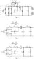
- this embodiment provides a power supply circuit 1, which includes: A rectifier module 11, a first diode D1, a second diode D2, a first inductor L1, a first capacitor C1, a freewheeling module 12, a main switch S, a third diode D3, a second inductor L2, and a second capacitor C2.
- the rectifier module 11 receives an AC voltage V ac and rectifies the AC voltage V ac to obtain a DC input voltage V in .
- the rectifier module 11 is a bridge-type uncontrolled rectification filtering circuit and includes two diode groups connected in parallel. Each diode group includes two diodes connected in series. The AC voltage V ac is connected between the two diodes of each diode group.
- the rectifier module 11 provides a DC input voltage V in , the input voltage V in being the absolute value of a sinusoidal voltage signal. In actual use, any structure that can rectify an AC voltage into a DC voltage is applicable to the present disclosure and is not limited by this embodiment.
- the cathode of the first diode D1 is connected to the non-inverting output end of the rectifier module 11, and the anode of the first diode D1 is connected to the cathode of the second diode D2; the anode of the second diode D2 is connected to the inverting output end of the rectifier module 11.
- first diode D1 and the second diode D2 with the same phase are connected in series, they are connected in parallel across the output ends of the rectifier module 11, to provide a current circuit.
- a first end of the first inductor L1 is connected to the cathode of the first diode D1, and a second end of the first inductor L1 is connected to a first end of the main switch S.
- an input end of the freewheeling module 12 is connected to the second end of the first inductor L1, and an output end of the freewheeling module 12 is connected to the first end of the first inductor L1.
- the freewheeling module 12 includes a freewheeling switch SF and a fourth diode D4 connected in series with each other.
- the freewheeling switch SF is an NMOS transistor.
- the drain of the freewheeling switch SF is connected to the second end of the first inductor, the source of the freewheeling switch SF is connected to the anode of the fourth diode D4, and the gate of the freewheeling switch SF receives a freewheeling switch control signal VSF.
- the cathode of the fourth diode D4 is connected to the first end of the first inductor L1.
- the position relationship between the freewheeling switch SF and the fourth diode D4 can be interchanged as long as they are connected in series. In actual use, any optional conduction freewheeling module is applicable to the present disclosure and is not limited by this embodiment.
- a lower electrode plate of the first capacitor C1 is connected to the anode of the first diode D1, and an upper electrode plate of the first capacitor C1 is connected to the second end of the first inductor L1.
- a first end of the second inductor L2 is connected to a second end of the main switch S, and a second end of the second inductor L2 is connected to the inverting output end of the rectifier module 11 via the second capacitor C2.
- the main switch S is an NMOS transistor, then the drain of the main switch S is connected to the second end of the first inductor L1, the source of the main switch S is connected to the first end of the second inductor L2, and the gate of the main switch S is connected to the main switch control signal Vs; in actual use, the connection port can be adjusted according to the specific device type, which will not be repeated here.
- both ends of the second capacitor C2 are the output voltage V o of the power supply circuit 1.
- the cathode of the third diode D3 is connected to the first end of the second inductor L2, and the anode of the third diode D3 is connected to the inverting output end of the rectifier module 11.
- the power supply circuit 1 further includes a main switch control module 13.
- the main switch control module 13 includes an operational amplifier 131 and a first comparator 132.
- the inverting input end of the operational amplifier 131 receives the output current i o of the power supply circuit 1
- the non-inverting input end of the operational amplifier 131 receives the first reference current I ref .
- the difference between the output current i o of the power supply circuit 1 and the first reference current I ref is amplified and output.
- the non-inverting input end of the first comparator 132 is connected to the output end of the operational amplifier 131, and the inverting input end of the first comparator 132 is connected to a carrier signal.
- the output signal of the operational amplifier 131 is compared with the carrier signal to generate a main switch control signal Vs.
- the carrier signal is a sawtooth wave; in actual use, the waveform of the carrier can be set as needed.
- the polarity relationship between the input end of the operational amplifier 131 and the corresponding input signal can be interchanged, and in this case, the polarity relationship between the input end of the first comparator 132 and the corresponding input signal also needs to be interchanged (that is, the non-inverting input end of the operational amplifier receives the output current of the power supply circuit, and the inverting input end of the operational amplifier receives the first reference current; the inverting input end of the first comparator is connected to the output end of operational amplifier, and the non-inverting input end of the first comparator receives the carrier signal), which can also achieve control of the main switch S of the present disclosure.
- any circuit structure capable of realizing the following logic is applicable to the present disclosure, not limited to devices and connection relationships listed in this embodiment: when the value (I ref -i o ) obtained by subtracting the output current i o from the first reference current I ref is greater than the value of the carrier signal, the main switch S is turned on; when the value (I ref -i o ) obtained by subtracting the output current i o from the first reference current I ref is less than the value of the carrier signal, the main switch S is turned off.
- the power supply circuit 1 further includes a freewheeling switch control module 14.
- the freewheeling switch control module 14 includes a second comparator 141 and an RS flip-flop 142.
- the inverting input end of the second comparator 141 receives a current i L1 of the first inductor L1
- the non-inverting input end of the second comparator 141 receives a second reference current i ref .
- the current i L1 of the first inductor L1 is compared with the second reference current i ref and the comparison result is output.
- the second reference current i ref is a sine wave current that is in phase with the AC voltage V ac .
- the set end of the RS flip-flop 142 is connected to the output end of the second comparator 141, and the reset end of the RS flip-flop 142 is connected to the main switch control signal Vs.
- the freewheeling switch control signal V SF is output. It should be noted that any circuit structure that can implement the following logic is applicable to the present disclosure, and is not limited to the devices and connection relationships listed in this embodiment: when the current i L1 of the first inductor L1 is less than the second reference current i ref and the main switch S is turned off, the freewheeling switch SF is turned on.
- control logic of the main switch S and the freewheeling switch SF is not limited to the examples listed in this embodiment. Any method that can control the main switch S and freewheeling switch SF based on this power supply circuit according to needs is applicable, and this embodiment is not limited.
- the present disclosure adopts a quadratic Buck PFC converter with a three-phase operating mode, which improves the load dynamic response speed and reduces the output current ripple.
- I L1 is the average value of the inductor current i L1 per cycle
- I L2 is the average value of the inductor current i L2 per cycle
- d is the conduction duty cycle of the main switch
- Ts is the switching period of the power supply circuit. It can be seen from formula 2 that I L1 ⁇ I L2 . Therefore, adding a freewheeling circuit to the first inductor L1 can reduce its loss during the freewheeling process, thereby making the power supply circuit more efficient.
- this embodiment provides an LED driving power supply, which includes: an LED load and a power supply circuit 1.
- the power supply circuit 1 adopts the power supply circuit structure of Embodiment 1, and the specific structure is not repeated here.
- the LED load is connected in parallel across the second capacitor C2, and the power supply circuit 1 supplies power to the LED load.
- the load dynamic response speed of the power supply circuit 1 is fast, and the output current ripple is small, which can make the LED load free of flicker.
- this embodiment provides a power supply method for a power supply circuit.
- the method is implemented based on the power supply circuit 1 of Embodiment 1.
- the first inductor L1 works in a Psuedo Continuous Conduction Mode (PCCM), and the second inductor L2 works in a Continuous Conduction Mode (CCM).
- the power supply method of the power supply circuit includes:
- stage A the working mode of the power supply circuit is divided into two stages: stage A and stage B.
- the power supply circuit in stage A includes two working modes: mode I and mode II.
- Mode I As shown in Fig. 5 , when the main switch S is turned on, there is no current flowing through the first inductor L1, and the first diode D1 is turned off; the first capacitor C1 supplies power to the second inductor L2 and the load, the second diode D2 is turned on, the third diode D3 is turned off, and the current i L2 of the second inductor L2 rises linearly.
- Mode II As shown in Fig. 6 , when the main switch S is turned off, the third diode D3 is turned on to provide a discharge circuit for the second inductor L2, the second inductor L2 supplies power to the load, and the current i L2 of the second inductor L2 decreases linearly.
- the power supply circuit works in stage B.
- the power supply circuit in stage B includes three working modes: mode III, mode IV and mode V. Within one switching cycle, assuming that the AC voltage V ac remains unchanged:
- the control logic of the main switch S and the freewheeling switch SF is as follows: when the value of the first reference current I ref minus the output current i o is greater than the value of the carrier signal, the main switch S is turned on; when the value of the first reference current I ref minus the output current i o is less than the value of the carrier signal, the main switch S is turned off.
- the carrier signal is a sawtooth wave.
- the freewheeling switch SF is turned on.
- the second reference current i ref is a sine wave in phase with the AC voltage V ac .
- this embodiment adopts a sine current reference control strategy, uses a voltage signal to control the conduction of the main switch S, and uses an inductor current feedback signal to control the conduction of the freewheeling switch SF.
- the output current signal i o is compared with the reference current I ref , and the compared signal is amplified through an operational amplifier to obtain an error signal as a non-inverting input of the first comparator.
- the error signal is compared with an inverting input carrier to obtain a drive control signal Vs for controlling the main switch S.
- the reference value i ref for the inductor current i L1 is a sine wave in phase with the AC voltage V ac .
- the reference value i ref is compared with the inductor current i L1 by the second comparator, and the compared result is used as the input of an S terminal (set end) of an RS flip-flop.
- the control signal of the main switch S is used as the input of an R terminal (reset end) of the RS flip-flop.
- a Q terminal of the RS flip-flop outputs a drive control signal V SF for the freewheeling switch SF, thereby realizing a voltage outer loop and a current inner loop to control the converter.
- waveform diagrams of major nodes in the power supply method according to this embodiment are provided. It can be seen that the first inductor L1 operates in the PCCM mode and the second inductor L2 operates in the CCM mode.
- this embodiment provides a power supply method for a power supply circuit based on the power supply circuit 1 according to Embodiment 1.
- the first inductor L1 operates in the PCCM mode and the second inductor L2 operates in a Discontinuous Conduction mode (DCM).
- the power supply method for the power supply circuit includes:
- the operating mode of the power supply circuit is divided into two stages: Stage A and Stage B.
- the power supply circuit When the input voltage V in is less than or equal to the voltage V C1 across the first capacitor, the power supply circuit operates in Stage A.
- the power supply circuit includes three operating modes: Mode I, Mode II and Mode VI. Among them, Mode I and Mode II are the same as Modes I and II in Embodiment 3 and will not be repeated here.
- Mode VI As shown in Fig. 11 , when both the main switch S and the freewheeling switch SF are turned off, the current i L2 of the second inductor L2 drops to zero, the third diode D3 is turned off, and the second capacitor C2 supplies power to the load.
- the power supply circuit in Stage B includes four operating modes: Mode III, Mode IV, Mode V and Mode VII. Among them, Modes III, IV and V are the same as Modes III, IV and V in Embodiment 3 and will not be repeated here.
- Mode VII As shown in Fig. 12 , when the main switch S is turned off and the freewheeling switch SF is turned on, the first inductor L1 enters a freewheeling state. The current i L1 of the first inductor L1 remains unchanged, the current i L2 of the second inductor L2 drops to zero, and the capacitor C2 supplies power to the load.
- Fig. 13 shows a waveform diagram of various main nodes in the power supply method of this embodiment. It can be seen that the first inductor L1 operates in the PCCM mode and the second inductor L2 operates in the DCM mode.
- the present disclosure has built six PFC converter simulation models based on PSIM simulation software for CCM/DCM-CCM/DCM quadratic Buck PFC converter and PCCM-CCM/DCM quadratic Buck PFC converter of the present disclosure.
- the AC voltage V ac , input current i in and output current i o waveform diagrams are obtained; among them, Fig. 14 is a waveform diagram corresponding to CCM-CCM working mode; Fig. 15 is a waveform diagram corresponding to CCM-DCM working mode; Fig. 16 is a waveform diagram corresponding to DCM-CCM working mode; Fig. 17 is a waveform diagram corresponding to DCM-DCM working mode; Fig.
- FIG. 18 is a waveform diagram corresponding to PCCM-CCM working mode of the present disclosure
- Fig. 19 is a waveform diagram corresponding to PCCM-DCM working mode of the present disclosure; from the above figures, it can be seen that the present disclosure has smaller output ripple.
- Figs. 20 to 25 three power supply circuits, that is, CCM-DCM, DCM-DCM and PCCM-DCM power supply circuits were selected to verify and analyze their load dynamic performance; among them, Fig. 20 shows the response time when the load power jumps from 20W to 10W under CCM-DCM working mode; Fig. 21 shows the response time when the load power jumps from 10W to 20W under CCM-DCM working mode; Fig.
- Fig. 22 shows the response time when the load power jumps from 20W to 10W under DCM-DCM working mode;
- Fig. 23 shows the response time when the load power jumps from 10W to 20W under DCM-DCM working mode of the present disclosure;
- Fig. 22 shows the response time when the load power jumps from 20W to 10W under PCCM-DCM working mode;
- Fig. 23 shows the response time when the load power jumps from 10W to 20W under PCCM-DCM working mode of the present disclosure. From the above figures, it can be seen that the present disclosure has a faster load dynamic response speed.
- the present disclosure provides a power supply circuit, including: a rectifier module, a first diode, a second diode, a first inductor, a first capacitor, a freewheeling module, a main switch, a third diode, a second inductor and a second capacitor.
- the rectifier module receives an AC voltage and rectifies the AC voltage to obtain a DC input voltage.
- the cathode of the first diode is connected to the non-inverting output end of the rectifier module, and the anode of the first diode is connected to the cathode of the second diode.
- the anode of the second diode is connected to the inverting output end of the rectifier module.
- a first end of the first inductor is connected to the cathode of the first diode, and a second end of the first inductor is connected to a first end of the main switch.
- An input end of the freewheeling module is connected to the second end of the first inductor, and an output end of the freewheeling module is connected to the first end of the first inductor.
- a lower electrode plate of the first capacitor is connected to the anode of the first diode, and an upper electrode plate of the first capacitor is connected to the second end of the first inductor; a first end of the second inductor is connected to a second end of the main switch, and a second end of the second inductor is connected to the inverting output end of the rectifier module via the second capacitor; the cathode of the third diode is connected to the first end of the second inductor, and the anode of the third diode is connected to the inverting output end of the rectifier module.
- the LED driving power supply, the power supply circuit and the power supply method of the present disclosure have two switches in the converter: a main switch and a freewheeling switch, that is, there are two control degrees of freedom, which makes it easier to optimize control parameter design; the present disclosure has a faster load dynamic response speed and smaller output current ripple. Therefore, the present disclosure effectively overcomes various disadvantages of the traditional technology and has high industrial values.
Landscapes
- Engineering & Computer Science (AREA)
- Power Engineering (AREA)
- Physics & Mathematics (AREA)
- Electromagnetism (AREA)
- Rectifiers (AREA)
Applications Claiming Priority (2)
| Application Number | Priority Date | Filing Date | Title |
|---|---|---|---|
| CN202110645429.6A CN115473424B (zh) | 2021-06-10 | 2021-06-10 | Led驱动电源、电源电路及供电方法 |
| PCT/CN2022/081954 WO2022257534A1 (zh) | 2021-06-10 | 2022-03-21 | Led驱动电源、电源电路及供电方法 |
Publications (2)
| Publication Number | Publication Date |
|---|---|
| EP4270751A1 true EP4270751A1 (de) | 2023-11-01 |
| EP4270751A4 EP4270751A4 (de) | 2024-09-04 |
Family
ID=84363509
Family Applications (1)
| Application Number | Title | Priority Date | Filing Date |
|---|---|---|---|
| EP22819139.1A Pending EP4270751A4 (de) | 2021-06-10 | 2022-03-21 | Led-ansteuerungsstromversorgung, stromversorgungsschaltung und stromversorgungsverfahren |
Country Status (3)
| Country | Link |
|---|---|
| EP (1) | EP4270751A4 (de) |
| CN (1) | CN115473424B (de) |
| WO (1) | WO2022257534A1 (de) |
Families Citing this family (2)
| Publication number | Priority date | Publication date | Assignee | Title |
|---|---|---|---|---|
| CN116365900B (zh) * | 2023-03-01 | 2023-11-03 | 西南交通大学 | 交流输入非对称式无桥降压型pfc变换器 |
| CN119834621B (zh) * | 2025-03-18 | 2025-08-08 | 深圳市盛迪瓦特电气有限公司 | 一种二极管电压应力改善电路和变换电路 |
Family Cites Families (11)
| Publication number | Priority date | Publication date | Assignee | Title |
|---|---|---|---|---|
| US7432614B2 (en) * | 2003-01-17 | 2008-10-07 | Hong Kong University Of Science And Technology | Single-inductor multiple-output switching converters in PCCM with freewheel switching |
| CN101552547B (zh) * | 2009-01-14 | 2011-07-20 | 西南交通大学 | 伪连续工作模式开关电源功率因数校正方法及其装置 |
| CN203027134U (zh) * | 2013-01-10 | 2013-06-26 | 中国矿业大学 | 一种三态升压型功率因数校正电路 |
| CN103647448B (zh) * | 2013-12-09 | 2016-01-06 | 杭州士兰微电子股份有限公司 | 集成降压-反激式高功率因数恒流电路及装置 |
| CN103997828B (zh) * | 2014-05-12 | 2016-04-27 | 上海大学 | 一种基于Buck电路的无电解电容LED驱动电源 |
| CN104753335A (zh) * | 2014-07-10 | 2015-07-01 | 西南交通大学 | 一种二次型Buck功率因数校正变换器 |
| CN106208684B (zh) * | 2016-08-24 | 2018-07-31 | 西南交通大学 | 一种单电感双输出开关变换器组合型控制方法及其装置 |
| CN108599564B (zh) * | 2018-04-25 | 2020-10-23 | 电子科技大学 | 一种电容电压断续模式电容串接式交错并联Bcuk PFC变换器 |
| CN108768192A (zh) * | 2018-06-26 | 2018-11-06 | 重庆大学 | 一种新型单相电流源型逆变器拓扑结构与调制方法 |
| CN110768527A (zh) * | 2019-12-03 | 2020-02-07 | 哈尔滨理工大学 | 一种基于二次Buck变换器的大变比降压型三相PFC电路 |
| CN112366936A (zh) * | 2021-01-12 | 2021-02-12 | 四川大学 | 一种低输出纹波功率因数校正变换器 |
-
2021
- 2021-06-10 CN CN202110645429.6A patent/CN115473424B/zh active Active
-
2022
- 2022-03-21 WO PCT/CN2022/081954 patent/WO2022257534A1/zh not_active Ceased
- 2022-03-21 EP EP22819139.1A patent/EP4270751A4/de active Pending
Also Published As
| Publication number | Publication date |
|---|---|
| CN115473424A (zh) | 2022-12-13 |
| CN115473424B (zh) | 2025-10-03 |
| EP4270751A4 (de) | 2024-09-04 |
| WO2022257534A1 (zh) | 2022-12-15 |
Similar Documents
| Publication | Publication Date | Title |
|---|---|---|
| US11722070B2 (en) | Alternating current to direct current conversion circuit | |
| CN102959843B (zh) | Dc/dc功率转换装置 | |
| EP4057491B1 (de) | Asymmetrischer halbbrückensperrwandler und stromversorgungssystem | |
| Belaguli et al. | Series-parallel resonant converter operating in discontinuous current mode. Analysis, design, simulation, and experimental results | |
| EP4270751A1 (de) | Led-ansteuerungsstromversorgung, stromversorgungsschaltung und stromversorgungsverfahren | |
| CN104079179A (zh) | 谐振变换器和直流电源 | |
| US20230327564A1 (en) | Asymmetric half-bridge flyback circuit-based converter and control method thereof | |
| Alcazar et al. | High voltage gain boost converter based on three-state switching cell and voltage multipliers | |
| CN111835208B (zh) | 一种具有pfc电路的开关电源 | |
| Chen et al. | A novel three level full bridge resonant DC-DC converter suitable for high power wide range input applications | |
| CN205356155U (zh) | 一种单管Buck-Boost-flyback升降压型电路 | |
| Vuchev et al. | Analysis of continuous current mode of an LLC resonant DC-DC converter at ZVS | |
| de Seixas et al. | The ZVS-PWM commutation cell applied to the DC-AC converter | |
| Gangavarapu et al. | Analysis and design of three phase single stage isolated Cuk based PFC converter | |
| Kumar et al. | A cascaded buck-flyback structure for high voltage step down applications | |
| CN206698116U (zh) | 一种降低开关管电流应力的高增益直流电压变换器 | |
| CN110112902A (zh) | 一种三相升降压型pfc整流电路 | |
| WO2022179564A1 (zh) | 无桥降压功率因素校正电路 | |
| Gou | Improved topologies towards existing types of single phase rectifiers | |
| CN106921295A (zh) | 一种降低开关管电流应力的高增益直流电压变换器 | |
| Qiao et al. | One-cycle controlled three-phase buck-derived rectifier | |
| CN118508781B (zh) | 一种单相可升降压电流源型逆变器及其使用方法 | |
| US20240243655A1 (en) | Power factor correction pfc circuit control method and pfc circuit | |
| CN110289639A (zh) | 一种级联式变流器及其控制方法和应用系统 | |
| Hwu et al. | Bridgeless Buck-Boost PFC Rectifier with Positive Output Voltage Suitable for LED Driving |
Legal Events
| Date | Code | Title | Description |
|---|---|---|---|
| STAA | Information on the status of an ep patent application or granted ep patent |
Free format text: STATUS: THE INTERNATIONAL PUBLICATION HAS BEEN MADE |
|
| PUAI | Public reference made under article 153(3) epc to a published international application that has entered the european phase |
Free format text: ORIGINAL CODE: 0009012 |
|
| STAA | Information on the status of an ep patent application or granted ep patent |
Free format text: STATUS: REQUEST FOR EXAMINATION WAS MADE |
|
| 17P | Request for examination filed |
Effective date: 20230726 |
|
| AK | Designated contracting states |
Kind code of ref document: A1 Designated state(s): AL AT BE BG CH CY CZ DE DK EE ES FI FR GB GR HR HU IE IS IT LI LT LU LV MC MK MT NL NO PL PT RO RS SE SI SK SM TR |
|
| A4 | Supplementary search report drawn up and despatched |
Effective date: 20240802 |
|
| RIC1 | Information provided on ipc code assigned before grant |
Ipc: H05B 45/375 20200101ALI20240729BHEP Ipc: H02M 1/34 20070101ALI20240729BHEP Ipc: H02M 3/155 20060101ALI20240729BHEP Ipc: H02M 1/42 20070101AFI20240729BHEP |
|
| DAV | Request for validation of the european patent (deleted) | ||
| DAX | Request for extension of the european patent (deleted) |