EP4257986A1 - Stromnebenschluss mit verringerter temperatur in bezug auf spannungsabfall - Google Patents
Stromnebenschluss mit verringerter temperatur in bezug auf spannungsabfall Download PDFInfo
- Publication number
- EP4257986A1 EP4257986A1 EP23164565.6A EP23164565A EP4257986A1 EP 4257986 A1 EP4257986 A1 EP 4257986A1 EP 23164565 A EP23164565 A EP 23164565A EP 4257986 A1 EP4257986 A1 EP 4257986A1
- Authority
- EP
- European Patent Office
- Prior art keywords
- metal clip
- landing pads
- landing
- pads
- electronic device
- Prior art date
- Legal status (The legal status is an assumption and is not a legal conclusion. Google has not performed a legal analysis and makes no representation as to the accuracy of the status listed.)
- Granted
Links
Images


Classifications
-
- H10W72/60—
-
- G—PHYSICS
- G01—MEASURING; TESTING
- G01R—MEASURING ELECTRIC VARIABLES; MEASURING MAGNETIC VARIABLES
- G01R15/00—Details of measuring arrangements of the types provided for in groups G01R17/00 - G01R29/00, G01R33/00 - G01R33/26 or G01R35/00
- G01R15/14—Adaptations providing voltage or current isolation, e.g. for high-voltage or high-current networks
- G01R15/146—Measuring arrangements for current not covered by other subgroups of G01R15/14, e.g. using current dividers, shunts, or measuring a voltage drop
-
- G—PHYSICS
- G01—MEASURING; TESTING
- G01R—MEASURING ELECTRIC VARIABLES; MEASURING MAGNETIC VARIABLES
- G01R1/00—Details of instruments or arrangements of the types included in groups G01R5/00 - G01R13/00 and G01R31/00
- G01R1/20—Modifications of basic electric elements for use in electric measuring instruments; Structural combinations of such elements with such instruments
- G01R1/203—Resistors used for electric measuring, e.g. decade resistors standards, resistors for comparators, series resistors, shunts
-
- G—PHYSICS
- G01—MEASURING; TESTING
- G01R—MEASURING ELECTRIC VARIABLES; MEASURING MAGNETIC VARIABLES
- G01R1/00—Details of instruments or arrangements of the types included in groups G01R5/00 - G01R13/00 and G01R31/00
- G01R1/02—General constructional details
- G01R1/04—Housings; Supporting members; Arrangements of terminals
- G01R1/0408—Test fixtures or contact fields; Connectors or connecting adaptors; Test clips; Test sockets
- G01R1/0425—Test clips, e.g. for IC's
-
- G—PHYSICS
- G01—MEASURING; TESTING
- G01R—MEASURING ELECTRIC VARIABLES; MEASURING MAGNETIC VARIABLES
- G01R31/00—Arrangements for testing electric properties; Arrangements for locating electric faults; Arrangements for electrical testing characterised by what is being tested not provided for elsewhere
- G01R31/26—Testing of individual semiconductor devices
- G01R31/2601—Apparatus or methods therefor
-
- G—PHYSICS
- G01—MEASURING; TESTING
- G01R—MEASURING ELECTRIC VARIABLES; MEASURING MAGNETIC VARIABLES
- G01R31/00—Arrangements for testing electric properties; Arrangements for locating electric faults; Arrangements for electrical testing characterised by what is being tested not provided for elsewhere
- G01R31/28—Testing of electronic circuits, e.g. by signal tracer
- G01R31/2801—Testing of printed circuits, backplanes, motherboards, hybrid circuits or carriers for multichip packages [MCP]
- G01R31/281—Specific types of tests or tests for a specific type of fault, e.g. thermal mapping, shorts testing
- G01R31/2815—Functional tests, e.g. boundary scans, using the normal I/O contacts
-
- H—ELECTRICITY
- H01—ELECTRIC ELEMENTS
- H01C—RESISTORS
- H01C1/00—Details
- H01C1/01—Mounting; Supporting
- H01C1/014—Mounting; Supporting the resistor being suspended between and being supported by two supporting sections
-
- H—ELECTRICITY
- H02—GENERATION; CONVERSION OR DISTRIBUTION OF ELECTRIC POWER
- H02M—APPARATUS FOR CONVERSION BETWEEN AC AND AC, BETWEEN AC AND DC, OR BETWEEN DC AND DC, AND FOR USE WITH MAINS OR SIMILAR POWER SUPPLY SYSTEMS; CONVERSION OF DC OR AC INPUT POWER INTO SURGE OUTPUT POWER; CONTROL OR REGULATION THEREOF
- H02M1/00—Details of apparatus for conversion
- H02M1/0003—Details of control, feedback or regulation circuits
- H02M1/0009—Devices or circuits for detecting current in a converter
-
- H10W72/621—
-
- H10W72/631—
-
- H10W72/634—
-
- H10W72/652—
-
- H10W90/764—
Definitions
- Power semiconductor devices and power electronic circuits constructed therefrom may be integrated into so-called power semiconductor modules (or power electronic modules).
- power electronic converters for example frequency converters, power inverters, etc.
- Power electronic converters constructed with the aid of power transistors for example MOSFETs or IGBTs
- IGBTs power transistors
- Another application involves inverters which, for example, convert direct current from solar plants into alternating current, so that the latter can be fed into the public power grid.
- inverters which, for example, convert direct current from solar plants into alternating current, so that the latter can be fed into the public power grid.
- Existing techniques for obtaining current measurements suffer from drawbacks and may be incapable of providing an accurate current measurement in large current conditions, such as power applications wherein the operational currents are on the order of 10A (amperes), 50A or more.
- the electronic device comprises a structured metallization layer comprising a plurality of contact pads that are electrically isolated from one another, and a metal clip connected in a current shunt measurement arrangement with a semiconductor device, wherein the metal clip comprises first, second and third landing pads, a first bridge span connected between the first and second landing pads, and second bridge span connected between the second and third landing pads, wherein the first, second third landing pads are respectively thermally conductively attached to first, second and third contact pads from the structured metallization layer, and wherein the second mounting pad is electrically floating.
- the metal clip comprises first, second and third landing pads, a first bridge span connected between the first and second landing pads, and a second bridge span connected between the second and third landing pads, wherein the metal clip is arranged to conduct a shunt current from the first landing pad to the third landing pad, wherein the first and second bridge spans comprise sections of a first conductive material that the shunt current must pass through, and wherein a temperature coefficient of the first conductive material is lower than that of the first, second and third landing pads.
- the embodiments described herein provide a metal clip that can be arranged as a current measurement shunt in an electronic device, such as a power module or a discrete package, and thereby used to measure an operational current of a component from the electronic device.
- the current measurement shunt advantageously comprises at least two bridge spans that each bridge a gap between landing pads of the current measurement shunt.
- the bridge spans can extend over and/or through an insulating region, such as a region of potting compound or epoxy.
- the landing pads of the current measurement shunt can comprise an electrically and thermally conductive metal such as copper, copper alloy, aluminum, etc., whereas the bridge spans comprise sections of resistive alloy, e.g., alloys comprising manganese and chromium.
- the multi-bridge configuration of the metal clip advantageously lowers the temperature of the material during operation by providing an intermediate heat dissipation region to extract heat that is generated from the resistive alloy by resistive heating. This allows for the metal clip to comprise a greater amount of resistive alloy and hence a higher electrical resistance without operating at dangerously high temperatures. The higher resistance in turn allows for more accurate current measurement.
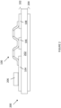
- a metal clip 100 is depicted, according to an embodiment.
- the metal clip 100 is mounted on a structured metallization layer 102 that comprises a plurality of contact pads.
- the metal clip 100 and the structured metallization layer 102 are shown from a plan-view perspective on the left side of Figure 1 and shown from a side-view perspective on the right side of Figure 1 .
- the structured metallization layer 102 can be formed from or comprise an electrically conductive metal, e.g., Cu, Ni, Ag, Au, Pd, Pt and alloys thereof. According to an embodiment, the structured metallization layer 102 is an upper-level metallization from a circuit carrier.
- the circuit carrier can be a power electronics carrier, such as a Direct Copper Bonding (DCB) substrate, a Direct Aluminum Bonding (DAB) substrate, or an Active Metal Brazing (AMB) substrate, or an Insulated Metal Substrate (IMS).
- DCB Direct Copper Bonding
- DAB Direct Aluminum Bonding
- AMB Active Metal Brazing
- IMS Insulated Metal Substrate
- a power electronics carrier may comprise an insulating substrate (not shown in Figure 1 ) underneath the structured metallization layer 102 of an electrically insulating material, e.g., ceramic material such as Al 2 O 3 (Alumina) AlN (Aluminum Nitride), or epoxy resin or polyimide in the case of an IMS substrate.
- the circuit carrier can be a printed circuit board (PCB), wherein the structured metallization layer 102 is formed on an electrically insulating substrate (not shown) that comprises a resin material such as FR-4.
- the structured metallization layer 102 is from a metal lead frame that is used in a discrete semiconductor package.
- the structured metallization layer 102 comprises first, second and third contact pads 104, 106, 108. Each of these contact pads from the structured metallization layer 102 are electrically isolated from one another. This electrical isolation may be provided by the underlying substrate of a circuit carrier. Moreover, this electrical isolation may be provided by a dielectric medium (not shown) that the metal clip 100 and the structured metallization layer 102 are embedded within.
- the dielectric medium may be an electrically insulating encapsulant material, e.g., a potting compound such as a silicone based potting compound in the case of power module, or a molding compound comprising epoxy, thermosetting plastic, polymer, etc., in the case of a discrete semiconductor package.
- the metal clip 100 is connected in a current shunt measurement arrangement with a semiconductor device.
- an operational current from the semiconductor device flows into the metal clip 100 as a shunt current 110.
- the voltage drop across the metal clip 100 is measured to extrapolate the magnitude of the operational current.
- the semiconductor device to which metal clip 100 is connected in a shunt arrangement with can be any of a wide variety of semiconductor devices, e.g., power transistor, diode, passive device, etc.
- the metal clip 100 is arranged to measure an operational current of a power semiconductor die.
- a power semiconductor die refers to a single device that is rated to accommodate voltages of at least 100 V (volts), and more typically voltages of 600 V, 1200 V or more and/or is rated to accommodate currents of at least 1A, and more typically currents of 10A, 50A, 100A or more.
- Examples of power semiconductor dies include discrete power diodes and discrete power transistor dies, e.g., MOSFETs (Metal Oxide Semiconductor Field Effect Transistors), IGBTs (Insulated Gate Bipolar Transistors), and HEMTs (High Electron Mobility Transistors), etc.
- the operational current can be an output current of a power semiconductor die, e.g., a source-drain current in the case of a MOSFET, emitter-collector current in the case of an IGBT, and so forth.
- the operational current of the device under measurement flows through the metal clip 100 as the shunt current 110 via the first and third contact pads 104, 108.
- a voltage measurement device may be connected between the first and third contact pads 104, 10 which correspond to first and second measurement nodes.
- the second contact pad 106 may be electrically floating as the shunt current 110 does not flow through the second contact pad 106 in the current measurement shunt arrangement.
- the metal clip 100 comprises first, second and third landing pads 112, 114, and 116.
- the first, second and third landing pads 112, 114, and 116 are sections of the metal clip 100 that are configured to be flush against and at least thermally connected to the contact pads of the structured metallization layer 102.
- the first, second and third landing pads 112, 114, and 116 may each comprise a substantially planar lower mounting surface, and the mounting surfaces from each of the first, second and third landing pads 112, 114, and 116 are substantially coplanar with one another.
- the first, second and third landing pads 112, 114, and 116 are respectively thermally conductively attached to the first, second and third contact pads 104, 106, 108 from the structured metallization layer 102.
- thermal coupling between the first, second and third landing pads 112, 114, and the first, second and third contact pads 104, 106, 108, respectively.
- a thermally conductive adhesive may be used to effectuate the connection between the first, second and third landing pads 112, 114, and 116 and the respective first, second and third contact pads 104, 106, 108.
- a joining material such as solder, sinter, conductive glue, etc. may be used to mechanically attach the metal clip 100 to each one of the first, second and third contact pads 104, 106, 108.
- attachment materials may also provide an electrically conducive connection, which allows for the operational current of the device under measurement to flow through the metal clip 100 via the first and third contact pads 104, 108.
- the second contact pad 106 may be electrically floating and thus does not require an electrically conductive joining material and/or the same joining material as the material used to join the first and third contact pads 104, 108.
- the material used to attach and thermally couple the second landing pad 114 to the second contact pad 106 may optionally include thermally conducive and non-electrically conductive materials such as thermal grease or thermal interface material.
- the metal clip 100 has a linear geometry whereby the shunt current 110 flows linearly between the first, second and third landing pads 112, 114, and 116. That is, the metal clip 100 is arranged so that a straight conduction path between the ends of the metal clip 100 exists along a current flow direction of the metal clip 100.
- a linear current in this context refers to the direction of current flow along one directional axis and can include currents that flow in multiple directions along another directional axis, e.g., in the depicted configuration the current flows linearly between the first and third landing pads 112, 116 along a lateral axis while changing direction along a vertical axis.
- the metal clip 100 comprises a first bridge span 118 connected between the first and second landing pads 112, 114, and a second bridge span 120 connected between the second and third landing pads 114, 116.
- the term bridge refers to a section of the metal clip 100 that the shunt current 110 must pass through when flowing between two landing pads.
- the first bridge span 118 is elevated from the first and second landing pads 112, 114, meaning that a lower surface of the first bridge span 118 is vertically offset from the mounting surface of the first and second landing pads 112, 114.
- the second bridge span 120 is elevated from the second and third landing pads 114, 116. This arrangement may allow for easier mounting of the metal clip 100. This arrangement is not necessary, however.
- the first and second bridge spans 118, 120 may be arranged to be coplanar with the first, second and third landing pads 112, 114, and 116.
- the first, second and third landing pads 112, 114, and 116 may be formed from a metal with low electrical resistance and high thermal conductivity. Examples of metals that meet this criterion include Cu, Al, Ag, Au, and alloys thereof. In a particular embodiment, the first, second and third landing pads 112, 114, and 116 are formed from copper or a copper alloy.
- the metal clip 100 can also comprise a coating or plating of different materials, e.g., Ni, Pd, Pt, or alloys thereof that are used as protective coatings and/or adhesion promotors.
- the sections of the metal clip 100 which form the first, second and third landing pads 112, 114, and 116 are provided by a uniform thickness sheet of metal, e.g., a planar sheet of copper, and the geometry of the first, second and third landing pads 112, 114, and 116 as described and depicted herein is created by metal processing techniques such as stamping, cutting, punching, etc.
- the first and second bridge spans 118, 120 comprise sections of a first material 122 that is different from the material which forms the first, second and third landing pads 112, 114, and 116.
- the sections of the first material 122 may be welded to the thermally and electrically conductive metal which forms the first, second and third landing pads 112, 114, and 116, for example.
- the first material 122 has a higher electrical resistivity than the material which forms the first, second and third landing pads 112, 114, and 116.
- the first material 122 may have an electrical resistivity that is between about 100 and 500 times greater than the electrical resistivity of the material which forms the first, second and third landing pads 112, 114, and 116.
- the sections of the first material 122 may account for between 90% to 99% of an overall electrical resistance of the metal clip 100. Additionally, the first material 122 has a lower temperature coefficient than the material which forms the first, second and third landing pads 112, 114, and 116. Temperature coefficient refers to the relationship between electrical resistivity of a material and the temperature of the material. Stated in numerical terms, the first material 122 may have a temperature coefficient of approximately 20 parts per million (ppm) per degrees Celsius at temperatures between 20° C (degrees Celsius) and 60° C. Examples of materials that meet this requirement include resistive alloys of manganese and resistive alloys chromium.
- the first material 122 is Zeranin ® , which is a CuMn7Sn alloy material.
- the temperature coefficient of the material which forms the first, second and third landing pads 112, 114, and 116 may be approximately 1,000-10,000 parts per million (ppm) per degrees Celsius and/or may be at least 100 times greater than that of the first material 122. Examples of materials that conform to this requirement include the above-listed electrically conductive metals such as Cu, Al, Ag, Au and certain alloys thereof.
- the material which forms the first, second and third landing pads 112, 114, and 116 has a temperature coefficient of 3,500-4,500 parts per million (ppm) per degrees Celsius.
- Examples of materials that conform to this requirement include pure copper (Cu) and certain electrically conductive alloys of copper.
- Cu pure copper
- the difference in temperature coefficient allows for precision in current measurement by maintaining a stable electrical resistance of the metal clip 100 over a wide operating range. As the metal clip 100 experiences resistive heating, e.g., in the case of a power applications wherein the magnitude of the operational current may exceed 1A, 10A or more, a voltage across the metal clip 100 does not significantly change and hence the accuracy of the current measurement remains high.
- the multi-bridge configuration of the metal clip 100 advantageously lowers the temperature to resistance ratio of the metal clip 100 in an electrical device that utilizes the metal clip 100 as a current measurement shunt. That is, the features of the metal clip 100 allow for the metal clip 100 to operate at a lower temperature for a given voltage drop across the metal clip 100. While the types of materials suitable for the first material 122 offer low temperature coefficients, many electronic devices are unable to accommodate a metal clip 100 that operates at high temperatures, e.g., temperatures 200° C or more. At these temperatures, dielectric mediums that encapsulate the metal clip 100, e.g., potting compounds or molding compounds, may mechanically fail and/or become detached from the metal clip 100.
- the multi-bridge configuration lowers the resistive heating temperature of the metal clip 100 by dividing the parts of the metal clip 100 that represent most of its electrical resistance and operate at the highest temperature.
- the material which forms the first, second and third landing pads 112, 114, and 116 has a high thermal conductivity, the heat generated by the first material 122 is extracted away and conducted through the first, second and third contact pads 104, 106, 108, which in turn may be thermally coupled to a heat sink.
- the multi-bridge configuration introduces an additional thermal conduction path into the middle of the resistive portion of the metal clip 100 whereby heat can be dissipated via the second contact pad 106.
- a very high load current e.g., 1A (amperes), 10A, or more while simultaneously requiring voltage differences of at least, 120 mV (Millivolts), 150mV, 200 mV or more across the current shunt to obtain an accurate measurement.
- the metal clip 100 offers a high degree of precision in electrical resistance in combination with a low area consumption.
- an important requirement for current measurement shunts is a low variation in electrical resistance across multiple nominally identical parts. That is, accurate current measurement is obtained when the resistance value of the metal clip 100 precisely conforms to a known value.
- One technique for maintaining a low variation in electrical resistance involves a post-processing step whereby a small amount of the first material 122 is removed to bring a tested resistance of the metal clip 100 into closer conformity with an expected value. Even still, there is a slight degree of electrical resistance variation after performing this technique.
- the multi-bridge configuration of the metal clip 100 is advantageous in this regard because the overall electrical resistance of the metal clip 100 can be tuned within the electrical resistance variation window of the post-processing step by removing the first material 122 from one or both of the first and second bridge sections 118, 120.
- producing two separate metal clips increases the potential for variation because each device is tuned for electrical resistance separately and thus the possible variation between any two of these clips can be up to twice as much as a single component counterpart.
- the metal clip 100 requires a smaller area footprint in comparison to two separate metal clips because the second landing pad 114 replaces the need for two separate landing pads and corresponding contact pads.
- the power electronics carrier 200 may be a DCB substrate, a DAB substrate, an AMB substrate, or an IMS substrate, for example.
- the power electronics carrier 200 comprises an electrically insulating substrate 202.
- the electrically insulating substrate 202 can comprise electrically insulating material, e.g., ceramic material such as Al 2 O 3 (Alumina) AlN (Aluminum Nitride).
- the power electronics carrier 200 comprises a structured metallization layer 102 disposed on an upper surface of the electrically insulating substrate 202 and a second metallization layer 204 disposed on a lower surface of the electrically insulating substrate 202.
- the second metallization layer 204 can comprise an electrically conductive metal and can be used to thermally couple the power electronics carrier 200 to a heat sink.
- the electronic device comprises the metal clip 100 mounted on the structured metallization layer 102 which corresponds to an upper-level metallization layer of the power electronics carrier 200.
- the electronic device additionally comprises a semiconductor die 206 mounted on the structured metallization layer 102.
- the metal clip 100, semiconductor die 206, and the power electronics carrier 200 may form part of an integrated power module, which may be configured as a power converter or inverter, for example.
- the semiconductor die 206 may be a power transistor die which forms a high-side switch or a low-side switch of a half-bridge circuit.
- the power module may comprise one or more driver dies that control a switching operation of the half-bridge circuit.
- the power module may comprise a plastic housing that surrounds an interior volume over the power electronics carrier 200, a potting compound such as a silicone based potting compound that fills the interior volume and encapsulates the elements mounted on the power electronics carrier 200, and conductive terminals that protrude out of the housing and provide externally accessible points of electrical contact.
- a plastic housing that surrounds an interior volume over the power electronics carrier 200
- a potting compound such as a silicone based potting compound that fills the interior volume and encapsulates the elements mounted on the power electronics carrier 200
- conductive terminals that protrude out of the housing and provide externally accessible points of electrical contact.
- the metal clip 100 is mounted on the power electronics carrier 200 in a current shunt measurement with the semiconductor die 206.
- the semiconductor die 206 may be a vertical power transistor die, e.g., MOSFET, IGBT, etc., that is mounted on the first contact pad 104 of the structured metallization layer 102 with a load terminal of the vertical power transistor, e.g., source, drain, collector, emitter, etc. facing and electrically connected to the first contact pad 104, e.g., by a solder connection.
- the metal clip 100 may be arranged as a shunt for a phase current of the power conversion circuit, meaning that the output current of the half-bridge circuit flows through the metal clip 100.
- a magnitude of the phase current can be obtained in the above-described manner by obtaining the voltage difference between the first and third contact pads 104, 108 of the structured metallization layer 102.
- Heat that is generated by the metal clip 100 during operation of the power conversion circuit is advantageously dissipated by all three of the first, second and third contact pads 104, 106, 108 from the power electronics carrier 200, which in turn may be thermally coupled to a cooling apparatus such as a heat sink.
- the metal clip 100 is depicted, according to two different embodiments.
- the metal clip 100 comprises the first and second bridge span 118, 120 being connected between the first, second and third landing pads 112, 114, and 116, as described above, and the first, second and third landing pads 112, 114, and 116 are respectively conductively attached to the first, second and third contact pads 104, 106, 108 from the structured metallization layer 102 in the same way as described above.
- the embodiments of Figure 3 have a different geometry as the previously disclosed embodiment.
- the metal clip 100 may have an angled geometry whereby the shunt current 110 of the metal clip 100 flows in a first direction between the first and second landing pads 112, 114 and in a second direction between the second and third landing pads 114, 116, and the first and second current flow directions are oriented transversely relative to one another.
- the metal clip 100 may be arranged to form a perpendicular angle at the second landing pad 114 such that the first and second current flow directions are perpendicular to one another.
- the metal clip 100 may have any non-linear geometry that redirects between the first and third landing pads 104, 108. Such an arrangement may be preferred in applications in which space constraints do not accommodate a linear geometry.
- the metal clip 100 may have a reversing geometry whereby the electrical current of the metal clip 100 flows in a first direction between the first and second landing pads 112, 114 and in a second direction between the second and third landing pads 114, 116, and the first and second directions are antiparallel to one another.
- Another way to describe the metal clip 100 is a U-shaped structure whereby the operational current flows between first and third landing pads 104, 108 that are immediately adjacent to one another. Such an arrangement may be preferred in applications in which space constraints do not accommodate other geometries.
- the geometry in Fig. 3B may be easier to manufacture, as the reversing geometry can be obtained by forming a central notch in a continuous structure.
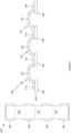
- the metal clip 100 is depicted, according to another embodiment.
- the metal clip 100 differs from the previously described embodiments in that it further comprises a third bridge span 124 connected between the third landing pad 116 and a fourth landing pad 126.
- the third bridge span 124 comprises a section of the first material 122 in a corresponding manner as the first and second bridge spans 118, 120.
- the fourth landing pad 126 is formed from the same thermally and electrically conductive metal as the first, second and third landing pads 112, 114, and 116.
- the multi-bridge concept of the metal clip 100 is extended to include an additional bridge span.
- the fourth landing pad 126 is attached to a fourth mounting pad 128 from the structured metallization layer 102.
- the fourth mounting pad 128 in combination with the first mounting pad 104 serve as first and second measurement modes that can be used to obtain a current measurement in the above-described manner.
- both the second and third contact pads 106, 108 can be electrically floating, and can both serve a purely cooling function.
- the three-bridge span configuration of Figure 4 represents a way to further increase to the electrical resistance of the metal clip 100 by adding additional spans of a resistive alloy while simultaneously providing the advantageous cooling benefit from interruptions in the resistive bridge material, as described above. This concept can be extended to greater numbers of bridge spans, e.g., four, five, six, etc., to obtain further increases in electrical resistance with the same advantageous cooling benefit being obtained.
- the metal clip 100 is depicted, according to another embodiment.
- the metal clip 100 of Figure 5 comprises first, second and third bridge spans 118, 120 and 124, and comprises first, second, third and fourth landing pads 112, 114, 116 and 126, in a similar manner as the embodiment disclosed above.
- the embodiment of Figure 4 has a meandering geometry wherein multiple sections having a reversing geometry as described with reference to Fig. 3B are strung together.
- This geometry represents a way to obtain the increased electrical resistance from multiple bridge sections with the first material 122, while also providing a compact footprint that may be preferred in certain applications.
- This meandering geometry concept can be extended to greater numbers of bridge spans, e.g., four, five, six, etc., to obtain further increases in electrical resistance with the same advantageous cooling benefit being obtained.
- Example 1 An electronic device, comprising: a structured metallization layer comprising a plurality of contact pads that are electrically isolated from one another; and a metal clip connected in a current shunt measurement arrangement with a semiconductor device, wherein the metal clip comprises first, second and third landing pads, a first bridge span connected between the first and second landing pads, and second bridge span connected between the second and third landing pads, wherein the first, second third landing pads are respectively thermally conductively attached to first, second and third contact pads from the structured metallization layer, and wherein the second mounting pad is electrically floating.
- Example 2 The electronic device of claim 1, wherein the first and second bridge spans are sections of a first conductive material that shunt current of the metal clip must pass through, and wherein a temperature coefficient of the first conductive material is lower than a temperature coefficient the first, second and third landing pads.
- Example 3 The electronic device of example 2, wherein the first conductive material is a resistive alloy with a temperature coefficient that is between 20 and 60 °C lower than that of the first, second and third landing pads, and wherein first, second and third landing pads are sections of copper or copper alloy.
- the first conductive material is a resistive alloy with a temperature coefficient that is between 20 and 60 °C lower than that of the first, second and third landing pads, and wherein first, second and third landing pads are sections of copper or copper alloy.
- Example 4 The electronic device of example 2, wherein the metal clip has a linear geometry whereby the shunt current of the metal clip flows linearly between the first, second and third landing pads.
- Example 5 The electronic device of example 2, wherein the metal clip has an angled geometry whereby the shunt current of the metal clip flows in a first direction between the first and second landing pads and in a second direction between the second and third landing pads, and wherein the first and second directions are oriented transversely relative to one another.
- Example 6 The electronic device of example 2, wherein the metal clip has a reversing geometry whereby the shunt current of the metal clip flows in a first direction between the first and second landing pads and in a second direction between the second and third landing pads, and wherein the first and second directions are antiparallel to one another.
- Example 7 The electronic device of example 1, wherein the metal clip further comprises a fourth landing pad, and a third bridge span connected between the third and fourth landing pads, wherein the fourth landing pad is attached to a fourth mounting pad from the structured metallization layer, and wherein the third mounting pad is electrically floating.
- Example 8 The electronic device of example 1, wherein the first bridge span is elevated from the first and second landing pads, and wherein the second bridge span is elevated from the second and third landing pads.
- Example 9 The electronic device of example 1, wherein the structured metallization layer is an upper-level metallization layer of a power electronics carrier, wherein the semiconductor device is a vertical power transistor die that is mounted on the upper-level metallization layer, and wherein the metal clip is connected to an output terminal of the vertical power transistor die.
- Example 10 The electronic device of example 10, wherein the electronic device is configured as a power module that comprises a power conversion circuit, and wherein the metal clip is arranged as a shunt for a phase current of the power conversion circuit.
- Example 11 A metal clip, comprising: first, second and third landing pads; a first bridge span connected between the first and second landing pads; and a second bridge span connected between the second and third landing pads, wherein the metal clip is arranged to conduct a shunt current from the first landing pad to the third landing pad, wherein the first and second bridge spans comprise sections of a first conductive material that the shunt current must pass through, and wherein a temperature coefficient of the first conductive material is lower than that of the first, second and third landing pads.
- Example 12 The metal clip of example 11, wherein the first conductive material is a resistive alloy with a temperature coefficient that is between 20 and 60 °C lower than that of the first, second and third landing pads, and wherein first, second and third landing pads are sections of copper or copper alloy.
- the first conductive material is a resistive alloy with a temperature coefficient that is between 20 and 60 °C lower than that of the first, second and third landing pads, and wherein first, second and third landing pads are sections of copper or copper alloy.
- Example 13 The metal clip of example 12, wherein the first conductive material is an alloy of manganese or an alloy of chromium.
- Example 14 The metal clip of example 11, wherein the metal clip has a linear geometry whereby the shunt current flows in a single linear direction between the first, second and third landing pads.
- Example 15 The metal clip of example 11, wherein the metal clip has an angled geometry whereby the shunt current flows in a first direction between the first and second landing pads and in a second direction between the second and third landing pads, and wherein the first and second directions are oriented transversely relative to one another.
- Example 16 The metal clip of example 11, wherein the metal clip has a reversing geometry whereby the shunt current of the metal clip flows in a first direction between the first and second landing pads and in a second direction between the second and third landing pads, and wherein the first and second directions are antiparallel to one another.
- Example 17 The metal clip of example 11, wherein the metal clip further comprises a fourth landing pad, and a third bridge span connected between the third and fourth landing pads, wherein the third bridge span comprises a section of the first conductive material that the shunt current must pass through.
- Example 18 The metal clip of example 11, wherein the first bridge span is elevated from the first and second landing pads and wherein the second bridge span is elevated from the second and third landing pads.
Landscapes
- Physics & Mathematics (AREA)
- General Physics & Mathematics (AREA)
- Measuring Instrument Details And Bridges, And Automatic Balancing Devices (AREA)
- Engineering & Computer Science (AREA)
- Computer Hardware Design (AREA)
- Microelectronics & Electronic Packaging (AREA)
- Power Engineering (AREA)
- Cooling Or The Like Of Semiconductors Or Solid State Devices (AREA)
Applications Claiming Priority (1)
| Application Number | Priority Date | Filing Date | Title |
|---|---|---|---|
| US17/715,434 US11810888B2 (en) | 2022-04-07 | 2022-04-07 | Current shunt with reduced temperature relative to voltage drop |
Publications (2)
| Publication Number | Publication Date |
|---|---|
| EP4257986A1 true EP4257986A1 (de) | 2023-10-11 |
| EP4257986B1 EP4257986B1 (de) | 2025-12-03 |
Family
ID=85778942
Family Applications (1)
| Application Number | Title | Priority Date | Filing Date |
|---|---|---|---|
| EP23164565.6A Active EP4257986B1 (de) | 2022-04-07 | 2023-03-28 | Stromnebenschluss mit verringerter temperatur in bezug auf spannungsabfall |
Country Status (3)
| Country | Link |
|---|---|
| US (1) | US11810888B2 (de) |
| EP (1) | EP4257986B1 (de) |
| CN (1) | CN116893290A (de) |
Citations (4)
| Publication number | Priority date | Publication date | Assignee | Title |
|---|---|---|---|---|
| US20100237982A1 (en) * | 2009-03-19 | 2010-09-23 | Vishay Dale Electronics, Inc. | Metal strip resistor for mitigating effects of thermal emf |
| US20140266269A1 (en) * | 2013-03-15 | 2014-09-18 | Infineon Technologies Ag | Multiple current sensor device, a multiple current shunt device and a method for providing a sensor signal |
| US20170089955A1 (en) * | 2014-09-25 | 2017-03-30 | Sanyo Electric Co., Ltd. | Electrical current detection device equipped with shunt resistor, and power supply device |
| US20210225565A1 (en) * | 2020-01-17 | 2021-07-22 | Wieland-Werke Ag | Resistor arrangement, measuring circuit comprising a resistor arrangement and methods for producing a strip-shaped material for the resistor arrangement |
Family Cites Families (3)
| Publication number | Priority date | Publication date | Assignee | Title |
|---|---|---|---|---|
| US8129789B2 (en) * | 2010-05-28 | 2012-03-06 | Infineon Technologies Ag | Current control using thermally matched resistors |
| DE102013219571B4 (de) | 2013-09-27 | 2019-05-23 | Infineon Technologies Ag | Leistungshalbleitermodul mit vertikalem Shunt-Widerstand |
| US12300643B2 (en) * | 2021-11-30 | 2025-05-13 | Infineon Technologies Ag | Solder stop feature for electronic devices |
-
2022
- 2022-04-07 US US17/715,434 patent/US11810888B2/en active Active
-
2023
- 2023-03-28 EP EP23164565.6A patent/EP4257986B1/de active Active
- 2023-04-06 CN CN202310358409.XA patent/CN116893290A/zh active Pending
Patent Citations (4)
| Publication number | Priority date | Publication date | Assignee | Title |
|---|---|---|---|---|
| US20100237982A1 (en) * | 2009-03-19 | 2010-09-23 | Vishay Dale Electronics, Inc. | Metal strip resistor for mitigating effects of thermal emf |
| US20140266269A1 (en) * | 2013-03-15 | 2014-09-18 | Infineon Technologies Ag | Multiple current sensor device, a multiple current shunt device and a method for providing a sensor signal |
| US20170089955A1 (en) * | 2014-09-25 | 2017-03-30 | Sanyo Electric Co., Ltd. | Electrical current detection device equipped with shunt resistor, and power supply device |
| US20210225565A1 (en) * | 2020-01-17 | 2021-07-22 | Wieland-Werke Ag | Resistor arrangement, measuring circuit comprising a resistor arrangement and methods for producing a strip-shaped material for the resistor arrangement |
Non-Patent Citations (1)
| Title |
|---|
| BOURNS: "Using Current Sense Resistors for Accurate Current Measurement", 1 January 2018 (2018-01-01), XP093073292, Retrieved from the Internet <URL:https://www.bourns.com/docs/technical-documents/technical-library/current-sense-pulse-power-high-power-resistors/application-notes/bourns_n1702_current_sense_accurate_measurement_appnote.pdf> [retrieved on 20230814] * |
Also Published As
| Publication number | Publication date |
|---|---|
| US20230326900A1 (en) | 2023-10-12 |
| CN116893290A (zh) | 2023-10-17 |
| EP4257986B1 (de) | 2025-12-03 |
| US11810888B2 (en) | 2023-11-07 |
Similar Documents
| Publication | Publication Date | Title |
|---|---|---|
| KR100852766B1 (ko) | 고 파워 밀도 디바이스를 위한 패키지 | |
| KR102585450B1 (ko) | 브레이징된 전기 전도성 층을 포함하는 칩 캐리어를 구비한 몰딩된 패키지 | |
| CN104517939B (zh) | 垂直分流电阻 | |
| US8680666B2 (en) | Bond wireless power module with double-sided single device cooling and immersion bath cooling | |
| CN102364345B (zh) | 具有所装配的电路载体的电路装置及相应功率半导体模块 | |
| US9385107B2 (en) | Multichip device including a substrate | |
| CN110060990B (zh) | 包括感测引线的化合物半导体装置 | |
| US11728251B2 (en) | Semiconductor power module with temperature sensors and shaped top plate to equalize current paths | |
| US12394692B2 (en) | Power circuit module | |
| US11610830B2 (en) | Power semiconductor module and method for fabricating the same | |
| EP4257943B1 (de) | Temperatursensoranordnung in einem halbleitermodul | |
| EP3886154A1 (de) | Halbleiterbauelement | |
| US11335660B2 (en) | Semiconductor module | |
| CN117099297A (zh) | 半导体装置 | |
| US11935875B2 (en) | Power module layout for symmetric switching and temperature sensing | |
| CN111312678A (zh) | 功率半导体模块和用于制造功率半导体模块的方法 | |
| US11810888B2 (en) | Current shunt with reduced temperature relative to voltage drop | |
| US20250273533A1 (en) | Electronic Device Having a Supply Terminal and a Thermal Bridge | |
| US20250321248A1 (en) | Electronic Component Having a Shunt Between a First Terminal and a Second Terminal | |
| CN118073311A (zh) | 具有电流感测的半导体封装 |
Legal Events
| Date | Code | Title | Description |
|---|---|---|---|
| PUAI | Public reference made under article 153(3) epc to a published international application that has entered the european phase |
Free format text: ORIGINAL CODE: 0009012 |
|
| STAA | Information on the status of an ep patent application or granted ep patent |
Free format text: STATUS: THE APPLICATION HAS BEEN PUBLISHED |
|
| AK | Designated contracting states |
Kind code of ref document: A1 Designated state(s): AL AT BE BG CH CY CZ DE DK EE ES FI FR GB GR HR HU IE IS IT LI LT LU LV MC ME MK MT NL NO PL PT RO RS SE SI SK SM TR |
|
| STAA | Information on the status of an ep patent application or granted ep patent |
Free format text: STATUS: REQUEST FOR EXAMINATION WAS MADE |
|
| 17P | Request for examination filed |
Effective date: 20240408 |
|
| RBV | Designated contracting states (corrected) |
Designated state(s): AL AT BE BG CH CY CZ DE DK EE ES FI FR GB GR HR HU IE IS IT LI LT LU LV MC ME MK MT NL NO PL PT RO RS SE SI SK SM TR |
|
| GRAP | Despatch of communication of intention to grant a patent |
Free format text: ORIGINAL CODE: EPIDOSNIGR1 |
|
| STAA | Information on the status of an ep patent application or granted ep patent |
Free format text: STATUS: GRANT OF PATENT IS INTENDED |
|
| INTG | Intention to grant announced |
Effective date: 20250630 |
|
| GRAS | Grant fee paid |
Free format text: ORIGINAL CODE: EPIDOSNIGR3 |
|
| GRAA | (expected) grant |
Free format text: ORIGINAL CODE: 0009210 |
|
| STAA | Information on the status of an ep patent application or granted ep patent |
Free format text: STATUS: THE PATENT HAS BEEN GRANTED |
|
| AK | Designated contracting states |
Kind code of ref document: B1 Designated state(s): AL AT BE BG CH CY CZ DE DK EE ES FI FR GB GR HR HU IE IS IT LI LT LU LV MC ME MK MT NL NO PL PT RO RS SE SI SK SM TR |
|
| REG | Reference to a national code |
Ref country code: CH Ref legal event code: F10 Free format text: ST27 STATUS EVENT CODE: U-0-0-F10-F00 (AS PROVIDED BY THE NATIONAL OFFICE) Effective date: 20251203 Ref country code: GB Ref legal event code: FG4D |
|
| REG | Reference to a national code |
Ref country code: DE Ref legal event code: R096 Ref document number: 602023009143 Country of ref document: DE |
|
| REG | Reference to a national code |
Ref country code: IE Ref legal event code: FG4D |