EP4255146B1 - Speicher und herstellungsverfahren dafür - Google Patents
Speicher und herstellungsverfahren dafür Download PDFInfo
- Publication number
- EP4255146B1 EP4255146B1 EP22908829.9A EP22908829A EP4255146B1 EP 4255146 B1 EP4255146 B1 EP 4255146B1 EP 22908829 A EP22908829 A EP 22908829A EP 4255146 B1 EP4255146 B1 EP 4255146B1
- Authority
- EP
- European Patent Office
- Prior art keywords
- active
- substrate
- layer
- initial
- dielectric layer
- Prior art date
- Legal status (The legal status is an assumption and is not a legal conclusion. Google has not performed a legal analysis and makes no representation as to the accuracy of the status listed.)
- Active
Links
Images


Classifications
-
- H—ELECTRICITY
- H10—SEMICONDUCTOR DEVICES; ELECTRIC SOLID-STATE DEVICES NOT OTHERWISE PROVIDED FOR
- H10B—ELECTRONIC MEMORY DEVICES
- H10B12/00—Dynamic random access memory [DRAM] devices
- H10B12/30—DRAM devices comprising one-transistor - one-capacitor [1T-1C] memory cells
- H10B12/48—Data lines or contacts therefor
- H10B12/485—Bit line contacts
-
- H—ELECTRICITY
- H10—SEMICONDUCTOR DEVICES; ELECTRIC SOLID-STATE DEVICES NOT OTHERWISE PROVIDED FOR
- H10B—ELECTRONIC MEMORY DEVICES
- H10B12/00—Dynamic random access memory [DRAM] devices
- H10B12/01—Manufacture or treatment
- H10B12/02—Manufacture or treatment for one transistor one-capacitor [1T-1C] memory cells
- H10B12/03—Making the capacitor or connections thereto
-
- H—ELECTRICITY
- H10—SEMICONDUCTOR DEVICES; ELECTRIC SOLID-STATE DEVICES NOT OTHERWISE PROVIDED FOR
- H10B—ELECTRONIC MEMORY DEVICES
- H10B12/00—Dynamic random access memory [DRAM] devices
- H10B12/01—Manufacture or treatment
- H10B12/02—Manufacture or treatment for one transistor one-capacitor [1T-1C] memory cells
- H10B12/05—Making the transistor
-
- H—ELECTRICITY
- H10—SEMICONDUCTOR DEVICES; ELECTRIC SOLID-STATE DEVICES NOT OTHERWISE PROVIDED FOR
- H10B—ELECTRONIC MEMORY DEVICES
- H10B12/00—Dynamic random access memory [DRAM] devices
- H10B12/30—DRAM devices comprising one-transistor - one-capacitor [1T-1C] memory cells
- H10B12/48—Data lines or contacts therefor
- H10B12/482—Bit lines
-
- H—ELECTRICITY
- H10—SEMICONDUCTOR DEVICES; ELECTRIC SOLID-STATE DEVICES NOT OTHERWISE PROVIDED FOR
- H10B—ELECTRONIC MEMORY DEVICES
- H10B12/00—Dynamic random access memory [DRAM] devices
- H10B12/30—DRAM devices comprising one-transistor - one-capacitor [1T-1C] memory cells
- H10B12/48—Data lines or contacts therefor
- H10B12/488—Word lines
-
- H—ELECTRICITY
- H10—SEMICONDUCTOR DEVICES; ELECTRIC SOLID-STATE DEVICES NOT OTHERWISE PROVIDED FOR
- H10B—ELECTRONIC MEMORY DEVICES
- H10B12/00—Dynamic random access memory [DRAM] devices
- H10B12/01—Manufacture or treatment
- H10B12/02—Manufacture or treatment for one transistor one-capacitor [1T-1C] memory cells
- H10B12/03—Making the capacitor or connections thereto
- H10B12/033—Making the capacitor or connections thereto the capacitor extending over the transistor
Definitions
- the disclosure relates to the technical field of semiconductors, in particular to a memory and a method for manufacturing the same.
- DRAM dynamic random access memory
- the dynamic random access memory is generally composed of multiple storage cells, each of which usually includes a transistor and a capacitor.
- the capacitor stores data information, and the transistor controls reading and writing of the data information in the capacitor.
- the width of a word line is small and the resistance of the word line is large, which makes the manufacture of the memory difficult and the performance poor.
- the embodiments of the disclosure provide a method for manufacturing a memory, in which a substrate is provided, and active pillars are formed on the substrate. A plurality of bit lines are formed in the substrate, and each bit line includes a plurality of straight line segments connected end to end in sequence. Adjacent straight line segments have an included angle therebetween.
- Each straight line segment of each bit line is electrically connected with at least two active pillars, so that the plurality of active pillars are staggered on the substrate, which can improve the density of the active pillars and increase the width of the gate, thereby improving the performance of the memory. Meanwhile, the bending number of each bit line is reduced, which is convenient for the manufacture of the memory.
- FIG. 1 it is a flowchart of a method for manufacturing a memory in an embodiment of the disclosure. The method includes the following operations.
- a substrate in which a plurality of bit lines arranged at intervals are formed in the substrate.
- Each bit line includes a plurality of straight line segments connected end to end in sequence, and adjacent line segments have an included angle therebetween.
- the substrate is used for providing a support, and may be a semiconductor substrate.
- the material of the semiconductor substrate may be one or more of silicon, germanium, silicon germanium, silicon carbide, Silicon on Insulator (SOI), Germanium on Insulator (GOI) or the like.
- Each bit line 10 includes a plurality of straight line segments connected end to end in sequence and adjacent line segments have an included angle therebetween, so that each bit line 10 is in a zigzag type.
- each bit line 10 includes a plurality of first straight line segments 11 extending in a second direction (direction Y1 shown in FIG. 2 ) and a plurality of second straight line segments 12 extending in a third direction ( direction Y2 shown in FIG. 2 ).
- Each second line segment 12 is connected with two adjacent first straight line segments 11, so that each bit line 10 is in form of a wavy polyline to make full use of the space of the substrate.
- the included angle formed by the second direction and the third direction may be 30° to 150°, for example 120°.
- a plurality of active pillars arranged at intervals and a plurality of insulating layers arranged at intervals are formed on the substrate.
- Each straight line segment of each bit line is electrically connected with at least two active pillars.
- the insulating layers extend along a first direction and cover the outer peripheral surfaces of the active pillars.
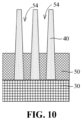
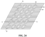
- the plurality of active pillars 40 and the plurality of insulating layers 50 are formed on the substrate 30.
- the active pillars 40 are filled with patterns in a top view in the embodiments of the disclosure.
- the top view is a partial view of the memory, for example, the view of a partial area enclosed by dashed lines in FIG. 2 .
- the plurality of active pillars 40 are arranged at intervals, and each straight line segment of each bit line 10 (referring to FIG. 2 ) is electrically connected with at least two active pillars 40.
- the active pillars 40 are in contact with the corresponding bit line 10 to achieve the electrical connection between the active pillars 40 and the bit line 10.
- the bit line 10 covers the orthographic projections of multiple active pillars 40 on the substrate 30.
- the entire bottom surface of the active pillar 40 is in contact with the bit line 10, and thus contact area between the active pillar 40 and the bit line 10 is large, thereby reducing the contact resistance between the active pillar 40 and the bit line 10.
- the active pillars 40 are used to form a source region, a drain region, and a channel region located between the source region and the drain region.
- the source region, drain region and channel region are arranged in a direction perpendicular to the substrate 30, and one of the source region and drain region is in contact with the substrate 30.
- the material of an active area may be a semiconductor material.
- the material of the active pillar 40 may be the same as or different from the material of the substrate 30.
- the substrate 30 and the active pillars 40 located on the substrate 30 are formed by etching the semiconductor material, in which the bit lines 10 are embedded bit lines.
- each seven active pillars 40 is regarded as a group, in which the centers of six active pillars 40 enclose into a virtual hexagon, i.e. the centers of the six active pillars 40 are respectively located at the six vertices of the virtual hexagon, and the center of the seventh active pillar 40 is located at the center of the virtual hexagon.
- the cross section of the active pillar 40 may not be in a shape of circular, which does not affect the arrangement of the plurality of active pillars 40.
- the density of the active pillars 40 can be increased.
- the density of the capacitors can be increased, thereby increasing the density of memories; on the other hand, the capacitor can be directly on the active pillar 40, without arranging a capacitor contact pad to transition the formation between the capacitor and the active pillar 40, thereby reducing the complexity of manufacturing the memory.
- the active pillars 40 are arranged in a square structure, it is necessary to manufacture capacitor contact pads on the active pillars 40, so as to arrange the capacitors in the hexagonal close-packed structure.
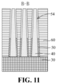
- the plurality of insulating layers 50 are arranged at intervals, extend in the first direction (direction X shown in FIG. 3 ) and cover on the outer peripheral surfaces of the active pillars 40. As shown in FIG. 3 , each insulating layer 50 corresponds to at least one active area located in the first direction and covers on the outer peripheral surface of at least one active area.
- the material of the insulating layer 50 may be silicon oxide, silicon nitride, silicon oxynitride or the like.
- each insulating layer 50 includes a first surrounding portion 51 and a first connecting portion 52.
- the first surrounding portion 51 is shown as an area surrounded by dashed lines in FIG. 3 , covers on the outer peripheral surface of the active pillar 40.
- the first connecting portion 52 is connected with two adjacent first surrounding portions 51 and extends in the first direction. That is, the first surrounding portion 51 corresponds to the active pillar 40, and surrounds the entire circumference of the active pillar 40, and the first connecting portion 52 is connected with two adjacent first surrounding portions 51 in the first direction.
- a first support layer is formed by filling between adjacent insulating layers.
- the first support layer 60 is formed between adjacent insulating layers 50 by a deposition process.
- the first support layer 60 fills up the space between adjacent insulating layers 50.
- the space between adjacent insulating layers 50 is filled by a process of chemical vapor deposition (CVD), physical vapor deposition (PVD), atomic layer deposition (ALD) or the like, to form the first support layer 60.
- CVD chemical vapor deposition
- PVD physical vapor deposition
- ALD atomic layer deposition
- the surface facing away from the substrate 30, of the first support layer 60 may be flush with the surface facing away from the substrate 30, of the insulating layer 50. That is, the top surface of the first support layer 60 is flush with the top surface of the insulating layer 50.
- the material of the first support layer 60 may be silicon oxide, silicon nitride or silicon oxynitride, and is different from the material of the insulating layer 50, so as to reduce the damage to the first support layer 60 when the insulating layer is subsequently removed.
- the material of the insulating layer 50 is silicon oxide (e.g., SiO 2 )
- the material of the first support layer 60 is silicon nitride (e.g., Si 3 N 4 ).
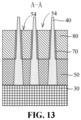
- part away from the substrate, of the insulating layer is removed to form a filling space which exposes part of the outer peripheral surface of the active pillar.
- part away from the substrate 30, of the insulating layer 50 is removed.
- this part of the insulating layer 50 is removed by etching.
- the middle part and upper part of the insulating layer 50 are removed to retain the lower part of the insulating layer 50.
- a filling space 54 is formed after part of the insulating layer 50 is removed.
- the filling space 54 exposes the outer peripheral surface of the active pillar 40.
- the filling space 54 exposes the outer peripheral surface of the channel region, so as to form a dielectric layer 70 and a conductive layer 80 on the outer peripheral surface of the channel region.
- a dielectric layer and a conductive layer are formed between parts exposed in the filling space and close to the substrate, of the active pillars to form a word line.
- the dielectric layer 70 is formed on part, exposed in the filling space 54 and close to the substrate 30, of the outer peripheral surface of the active pillar 40, and a conductive layer 80 is formed on the outer peripheral surface of the dielectric layer 70.
- the conductive layer 80 is formed by filling between the dielectric layer 70 and the first support layer 60.
- the conductive layer 80 and the dielectric layer 70 form a word line.
- the dielectric layer 70 and the conductive layer 80 surrounding the outer peripheral surface of the dielectric layer 70 form a gate. That is, the gate is part of the word line 20.
- the word line 20 extends in the first direction.
- the dielectric layer 70 may be an oxide layer, and forms a gate oxide layer.
- the material of the conductive layer 80 may be a metal, and the conductive layer 80 surrounding the outer peripheral surface of the dielectric layer 70 forms a gate conductive layer.
- the included angle between the second direction and the first direction shown in FIG. 2 is 60°
- the included angle between the third direction and the first direction is 60°
- a first pitch between adjacent word lines 20 is equal to a second pitch between adjacent bit lines 10.
- forming the dielectric layer and the conductive layer between the active pillars exposed in the filling space and close to the substrate to form the word line (S500) may include the following operations.
- part exposed in the filling space 54 and close to the substrate 30, of the outer peripheral surface of the active pillar 40 is at least removed to thin the active pillar 40 and enlarge the filling space 54, thereby increasing the space for forming a gate and improving the forming quality of the gate.
- all the part exposed in the filling space 54, of the active pillar 40 is etched by a process such as wet etching, so that all the outer peripheral surface of the active pillar 40 exposed in the filling space 54 is etched to thin the active pillar 40 and increase the volume of the filling space 54.
- Thinning the active pillar 40 means that the radial distance of the active pillar 40 is reduced, i.e. the diameter of the active pillar 40 is reduced after etching.
- the etched active pillar 40 is in the region of the active pillar 40 before etching.
- the dielectric layer 70 is formed on part exposed in the filling space 54 and close to the substrate 30, of the outer peripheral surface of the active pillar 40. That is, the dielectric layer 70 is formed on the outer peripheral surface of the active pillar 40 located at the lower part of the filling space 54, circumferentially surrounds and covers this part of the active pillar 40. There is no contact between the dielectric layer 70 and the first support layer 60 to provide a space required for forming the conductive layer 80.
- the dielectric layer 70 is formed on the outer peripheral surface exposed in the filling space 54, of the active pillar 40 by a deposition process. Then, the dielectric layer 70 located on part away from the substrate 30, the active pillar 4 is removed by etching with controlling the parameters in the etching process, to retain the required dielectric layer 70.
- the conductive layer is formed on the outer peripheral surface of the dielectric layer, and fills between the dielectric layer and the first support layer.
- the conductive layer 80 is formed on the outer peripheral surface of the dielectric layer 70 by depositing, and fills between the dielectric layer 70 and the first support layer 60. That is, the conductive layer 80 fills up the space between the dielectric layer 70 and the first support layer 60.
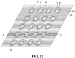
- the conductive layer 80 includes a second surrounding portion 81 surrounding the dielectric layer 70 and a second connecting portion 82 connecting adjacent second surrounding portions 81.
- the second surrounding portion 81 is shown as an area surrounded by dotted lines in FIG. 12 .
- the second surrounding portion 81 and the dielectric layer 70 constitute a gate.
- the conductive layer 80 and the dielectric layer 70 constitute the word line 20 (referring to FIG. 2 ), that is, part of the word line 20 serves as the gate.
- the conductive layer 80 further includes an extension portion connected to the outer side of the second surrounding portion 81 located at outermost side, in which the outer side refers to one side of the outermost second surrounding portion 81 away from other second surrounding portions 81.
- the left side of the second surrounding portion 81 located at the leftmost side is connected with one extension portion and the right side thereof is connected with the second connecting portion 82; the right side of the second surrounding portion 81 located at the rightmost side is connected with one extension portion, and the left side thereof is connected with the second connecting portion 82.
- the formation of the conductive layer 80 filling between the dielectric layer 70 and the first support layer 60, on the outer peripheral surface of the dielectric layer 70 may include the following operations.
- An initial conductive layer is deposited in the enlarged filling space 54.
- the initial conductive layer fills between the dielectric layer 70 and the first support layer 60 and covers the dielectric layer 70.
- the initial conductive layer is deposited between the dielectric layer 70 and the first support layer 60, and also covers the dielectric layer 70. For example, the initial conductive layer fills up the enlarged filling space 54.
- the initial conductive layer located on the dielectric layer 70 is removed to expose the dielectric layer 70, while the remaining part of the initial conductive layer forms the conductive layer 80.
- the surface facing away from the substrate 30, of the conductive layer 80 is flush with the surface facing away from the substrate 30, of the dielectric layer 70.
- the initial conductive layer located on the side facing away from the substrate 30 of the dielectric layer 70 is removed by an etching process, and the remaining part of the initial conductive layer forms the conductive layer 80.
- the upper surface of the conductive layer 80 is flush with the upper surface of the dielectric layer 70. That is, the required conductive layer 80 is formed by depositing and etching back.
- each bit line 10 in the substrate 30 includes the plurality of straight line segments connected end to end in sequence, and the adjacent straight line segments have the included angle therebetween.
- the density of the active pillars 40 can be improved by arranging the plurality of active pillars 40 in the staggered manner on the substrate 30, thereby improving the performance of the memory.
- At least two active pillars 40 are electrically connected to each straight line segment of each bit line 10, thereby reducing the bending number of each bit line 10 and facilitating the manufacture of the memory.
- the insulating layer 50 covers the outer peripheral surface of the active pillar 40.
- the dielectric layer 70 and the conductive layer 80 are formed between the exposed active pillars 40.
- the dielectric layer 70 and the conductive layer 80 constitute the gate, and the plurality of active pillars 40 are staggered on the substrate 30, which increases the width of the gate in the radial direction of the active pillar 40, improves the forming quality of the gate, reduces the resistance of the gate and further improves the performance of the memory.
- the operation (S200) that the plurality of active pillars arranged at intervals and the plurality of insulating layers arranged at intervals are formed on the substrate, in which each straight line segment of each bit line is electrically connected with at least two active pillars, and the insulating layers extend along the first direction and cover the outer peripheral surfaces of the active pillars, may include the following operations.
- Each active line corresponds to and is electrically connected one bit line.
- the plurality of active lines 41 arranged at intervals are formed by an etching process, in which the plurality of active lines 41 are parallel to each other.
- Each active line 41 corresponds to one bit line 10 and is electrically connected to the corresponding bit line 10 to achieve the electrical connection between the active line 41 and the bit line 10.
- each active line 41 includes a plurality of first active segments extending in the second direction, and a plurality of second active segments extending in the third direction.
- One second active segment is connected with two adjacent first active segments.
- the first active segment corresponds to and is in contact with the first straight line segment of the bit line 10
- the second active segment corresponds to and is in contact with the second straight line segment of the bit line 10.
- an initial insulating layer is formed on the substrate, and fills between adjacent active lines.
- an initial insulating layer 53 is deposited on the substrate 30, and fills between the active lines 41 to isolate the active lines 41 from each other. Specifically, the initial insulating layer 53 is deposited to fill between and cover the active lines 41. Then, the initial insulating layer 53 located on the active lines 41 is removed by etching to expose the active lines 41.
- part of the initial insulating layer and part of each active line are removed to form a plurality of first grooves arranged at intervals.
- the first grooves divide each active line into multiple active pillars.
- the remaining part of the initial insulating layer forms part of the first surrounding portion, and the first connecting portion connecting the first surrounding portion.
- the initial insulating layer 53 and the active lines 41 are etched to form the plurality of first grooves 42 arranged at intervals.
- the first grooves 42 extend in the first direction, and divide each active line 41 into multiple active pillars 40.
- the initial insulating layer 53 and part of the active line 41 are removed to form a plurality of initial grooves 43 arranged at intervals and extending in the first direction.
- the initial groove 43 exposes the substrate 30, and has a substantially constant width equal in the first direction.
- part exposed in the initial grooves 43 of the initial insulating layer 53 is removed to thin the initial insulating layer 53 located between adjacent initial grooves 43 to form the first grooves 42.
- the initial insulating layer 53 exposed in the initial groove 43 is etched to thin the initial insulating layer 53.
- the thinned initial insulating layer 53 forms the first connecting portion 52 (referring to FIG. 3 ) and part of the first surrounding portion 51.
- the surface area exposed in the initial grooves 43, of the active pillar 40 is increased, and the enlarged initial grooves 43 serve as the first grooves 42.
- the cross section of the active pillar 40 is in a quadrilaterallike shape.
- the cross section of the active pillar 40 is in a shape of a parallelogram or a rhombus.
- the active pillar 40 exposed in the first groove 42 is etched by a wet etching with an alkaline solution, so that the outer peripheral surface of each active pillar 40 is fillet-transitioned.
- the active pillar 40 is an approximate cylinder or an elliptic cylinder.
- the alkaline solution may be a potassium hydroxide solution or a SC1 solution. This solution has a faster reaction rate at sharp corners, which can make the corners of the active pillar 40 with the quadrilateral cross-sectional shape rounded, and make the dielectric layer 70 and the conductive layer 80 formed subsequently more uniform, improving the quality of the structure formed subsequently.
- part of the first surrounding portion is formed on the outer peripheral surface exposed in the first groove, of the active pillar.
- part of the first surrounding portion 51 is formed on the outer peripheral surface of the active pillar 40 by a thermal oxidation process.
- the first surrounding portion 51 covering the outer peripheral surface of the active pillar 40 is formed by this operation and the previous operation.
- the method further includes an operation of forming a second support layer covering the conductive layer in the remaining part of the filling space, after the dielectric layer and the conductive layer are formed between the active pillars exposed in the filling space and close to the substrate to form the word line (S500).
- the second support layer 90 is deposited on the conductive layer 80 and the dielectric layer 70 to insulate and isolate the conductive layer 80.
- the second support layer 90 fills up the remaining part of the filling space 54, and the surface away from the substrate 30, of the active pillar 40 is exposed.
- the material of the second support layer 90 may be the same as the material of the first support layer 60, so that the second support layer 90 is integrated with the first support layer 60, reducing or avoiding delamination or separation between the second support layer 90 and the first support layer 60.
- the surface facing away from the substrate 30, of the second support layer 90 may be flush with the surface facing away from the substrate 30, of the first support layer 60.
- the method further includes an operation of, on each active pillar, forming a capacitor electrically connected to this active pillar, the capacitor being aligned with this corresponding active pillar, after the dielectric layer and the conductive layer are formed between the active pillars exposed in the filling space and close to the substrate to form the word line (S500).
- the bottom surface of the capacitor is in contact with and aligned with the top surface of the active pillar 40, which realizes the electric connection between the capacitor and the active pillar 40 on the one hand, and ensures the contact area between the capacitor and the active pillar 40 on the other hand, thereby reducing the contact resistance between the capacitor and the active pillar 40.
- the memory includes a substrate 30, an active pillar 40, an insulating layer 50, a dielectric layer 70, a conductive layer 80, and a support layer.
- the substrate 30 is used for providing support, and may be a semiconductor substrate.
- the material of the semiconductor substrate may be one or more of silicon, germanium, silicon germanium, silicon carbide, Silicon on Insulator (SOI), Germanium on Insulator (GOI), or the like.
- a plurality of bit lines 10 arranged at intervals are formed in the substrate 30 (referring to FIG. 2 ).
- Each bit line 10 includes a plurality of straight line segments connected end to end in sequence, and adjacent line segments have an included angle therebetween, so that each bit line 10 is in a type of a zigzag line.
- the plurality of straight line segments included by each bit line 10 include a plurality of first straight line segments 11 extending in a second direction and a plurality of second straight line segments 12 extending in a third direction.
- One second straight line segment 12 connects two first straight line segments 11 adjacent to this one second straight line segment, so that each bit line 10 is in form of a wavy polyline to make full use of the space of the substrate.
- the included angle formed by the first direction and the second direction may be 30° to 150°, for example 120°.
- the plurality of active pillars 40 are formed on the substrate 30 and arranged at intervals.
- Each straight line segment of each bit line 10 is electrically connected with at least two active pillars 40.
- the active pillar 40 is in contact with the bit line 10 to achieve the electrical connection between the active pillar 40 and the bit line 10.
- the bit line 10 covers the orthographic projections of multiple active pillars 40 on the substrate 30.
- the entire bottom surface of the active pillar 40 is in contact with the bit line 10, and the contact area between the active pillar 40 and the bit line 10 is large, thereby reducing the contact resistance between the active pillar 40 and the bit line 10.
- each seven active pillars 40 is regarded as a group, in which the centers of six active pillars 40 enclose into a virtual hexagon, i.e. the centers of the six active pillars 40 are respectively located at the six vertices of the virtual hexagon, and the center of the seventh active pillar 40 is located at the center of the virtual hexagon.
- the density of the active pillars 40 can be increased.
- the density of the capacitors can be increased, thereby increasing the density of memories; on the other hand, the capacitor can be directly on the active pillar 40 without arranging a capacitor contact pad to transition the formation between the capacitor and the active pillar 40, thereby reducing the complexity of manufacturing the memory.
- the active pillars 40 are arranged in a square structure, it is necessary to manufacture capacitor contact pads on the active pillars 40, so as to arrange the capacitors in a hexagonal close-packed structure.
- a plurality of insulating layers 50 are also formed on the substrate 30, arranged at intervals and extend in the first direction. Each insulating layer 50 covers the outer peripheral surface of the lower region of the active pillar 40 in its extension direction.
- the lower region of the active pillar 40 refers to a region of the active pillar 40 close to the substrate 30.
- the dielectric layer 70 is formed on the outer peripheral surface of the middle region of the active pillar 40. That is, the dielectric layer 70 covers the outer peripheral surface of the middle region of the active pillar 40.
- a plurality of conductive layers 80 arranged at intervals are provided on the insulating layer 50.
- a conductive layer 80 extends in the first direction and covers the outer peripheral surface of the dielectric layer 70.
- the conductive layer 80 and the dielectric layer 70 form a word line.
- the included angle between the second direction and the first direction is 60°
- the included angle between the third direction and the first direction is 60°
- a first pitch between adjacent word lines 20 is equal to a second pitch between adjacent bit lines 10.
- the support layer fills between the insulating layers 50, between the conductive layers 80, and between upper regions of the active pillars 40.
- the support layer isolates each insulating layer 50, each conductive layer 80, and each active pillar 40.
- the support layer includes a first support layer 60 and a second support layer 90.
- the first support layer 60 fills between the insulating layers 50, between the conductive layers 80, and extends between the upper regions of the active pillars 40.
- the second support layer 90 fills between the first support layer 60 and the upper region of the active pillar 40.
- each bit line 10 in the substrate 30 includes the plurality of straight line segments connected end to end in sequence, and adjacent straight line segments have the included angle therebetween.
- the density of the active pillars 40 can be improved, which improves the performance of the memory.
- Each straight line segment of each bit line 10 is electrically connected with at least two active pillars 40, which reduces the bending number of of each bit line 10 and facilitates the manufacture of the memory.
- the dielectric layer 70 and part of the conductive layer 80 form the gate covering the outer peripheral surface of the active pillar 40, and the plurality of active pillars 40 are staggered on the substrate 10, which increases the width of the gate in the radial direction of the active pillar 40, thereby improving the forming quality of the gate, reducing the resistance of the gate and further improving the performance of the memory.
Landscapes
- Engineering & Computer Science (AREA)
- Manufacturing & Machinery (AREA)
- Semiconductor Memories (AREA)
Claims (11)
- Verfahren zur Herstellung eines Speichers, umfassend:Bereitstellen eines Substrats (30), wobei eine Mehrzahl von in Intervallen angeordneten Bitleitungen (10) in dem Substrat (30) ausgebildet sind, jede Bitleitung (10) eine Mehrzahl von Ende an Ende in Reihe verbundenen geraden Leitungssegmenten (11, 12) umfasst, und benachbarte gerade Leitungssegmente (11, 12) einen eingeschlossenen Winkel dazwischen aufweisen;Ausbilden einer Mehrzahl von in Intervallen angeordneten aktiven Säulen (40) und einer Mehrzahl von in Intervallen angeordneten Isolierschichten (50) auf dem Substrat (30), wobei jedes gerade Leitungssegment (11, 12) jeder Bitleitung (10) mit wenigstens zwei aktiven Säulen (40) elektrisch verbunden ist, und jede Isolierschicht (50) sich in einer ersten Richtung erstreckt und eine äußere □mfangsfläche der aktiven Säule (40) bedeckt; dadurch gekennzeichnet, dass das Verfahren ferner Folgendes umfasst:Füllen einer ersten Trägerschicht (60) zwischen benachbarten Isolierschichten (50);Entfernen eines Teils der Isolierschicht (50) von dem Substrat (30) weg, um einen Füllraum (54) auszubilden, wobei der Füllraum (54) einen Teil der äußeren □mfangsfläche der aktiven Säule (40) freilegt; undAusbilden einer dielektrischen Schicht (70) und einer leitenden Schicht (80) zwischen im Füllraum (54) und nahe dem Substrat (30) freiliegenden Teilen der aktiven Säulen (40), um eine Wortleitung (20) auszubilden.
- Verfahren nach Anspruch 1, wobei jede Isolierschicht (50) einen ersten umgebenden Abschnitt (51), der die äußere □mfangsfläche der aktiven Säule (40) bedeckt, und einen ersten Verbindungsabschnitt (52), der zwei benachbarte erste umgebende Abschnitte (51) verbindet und sich in der ersten Richtung erstreckt, umfasst.
- Verfahren nach Anspruch 2, wobei das Ausbilden der Mehrzahl von in Intervallen angeordneten aktiven Säulen (40) und der Mehrzahl von in Intervallen angeordneten Isolierschichten (50) auf dem Substrat (30), wobei jedes gerade Leitungssegment (11, 12) jeder Bitleitung (10) mit wenigstens zwei aktiven Säulen (40) elektrisch verbunden ist und die Isolierschicht (50) sich in der ersten Richtung erstreckt und die äußere □mfangsfläche der aktiven Säule (40) bedeckt, Folgendes umfasst:Ausbilden einer Mehrzahl von in Intervallen auf dem Substrat (30) angeordneten aktiven Leitungen (41), wobei jede aktive Leitung (41) einer Bitleitung (10) entspricht und mit dieser elektrisch verbunden ist;Ausbilden einer anfänglichen Isolierschicht (53) auf dem Substrat (30), wobei die anfängliche Isolierschicht (53) zwischen benachbarte aktive Leitungen (41) gefüllt wird;Entfernen eines Teils der anfänglichen Isolierschicht (53) und eines Teils jeder aktiven Leitung (41), um eine Mehrzahl von in Intervallen angeordneten ersten Nuten (42) auszubilden, wobei die Mehrzahl von ersten Nuten (42) die aktive Leitung (41) in eine Mehrzahl von aktiven Säulen (40) unterteilt; undAusbilden eines Teils des ersten umgebenden Abschnitts (51) auf einem in den ersten Nuten (42) der äußeren □mfangsfläche der aktiven Säule (40) freiliegenden Teil.
- Verfahren nach Anspruch 3, wobei das Entfernen eines Teils der anfänglichen Isolierschicht (53) und eines Teils jeder aktiven Leitung (41), um eine Mehrzahl von in Intervallen angeordneten ersten Nuten (42) auszubilden, wobei die Mehrzahl von ersten Nuten (42) die aktive Leitung (41) in die Mehrzahl von aktiven Säulen (40) unterteilt, Folgendes umfasst:Entfernen eines Teils der anfänglichen Isolierschicht (53) und eines Teils jeder aktiven Leitung (41), um eine Mehrzahl von in Intervallen angeordneten und sich in der ersten Richtung erstreckenden anfänglichen Nuten (43) auszubilden; undEntfernen eines in den anfänglichen Nuten (43) freiliegenden Teils der anfänglichen Isolierschicht (53), um die zwischen benachbarten anfänglichen Nuten (43) liegende anfängliche Isolierschicht (53) zu verdünnen, um die ersten Nuten (42) auszubilden.
- Verfahren nach Anspruch 4, wobei die aktive Säule (40), wenn man eine Ebene parallel zum Substrat (30) als Querschnitt nimmt, einen Querschnitt in Form eines Vierecks aufweist, und
das Verfahren ferner Folgendes umfasst:
Entfernen eines in den ersten Nuten (42) freiliegenden Teils der aktiven Säule (40), um die äußere □mfangsfläche der aktiven Säule (40) zu verrunden, nach Entfernen eines in den anfänglichen Nuten (43) freiliegenden Teils der anfänglichen Isolierschicht (53), um die zwischen benachbarten anfänglichen Nuten (43) liegende anfängliche Isolierschicht (53) zu verdünnen, um die ersten Nuten (42) auszubilden. - Verfahren nach Anspruch 5, wobei der in den ersten Nuten (42) freiliegende Teil der aktiven Säule (40) durch eine Nassätzung mit einer alkalischen Lösung geätzt wird.
- Verfahren nach Anspruch 3, wobei der Teil des ersten umgebenden Abschnitts (51) auf der äußeren □mfangsfläche der aktiven Säule (40) durch einen thermischen Oxidationsprozess ausgebildet wird.
- Verfahren nach Anspruch 1, wobei das Ausbilden der dielektrischen Schicht (70) und der leitenden Schicht (80) zwischen im Füllraum (54) und nahe dem Substrat (30) freiliegenden Teilen der aktiven Säulen (40), um die Wortleitung (20) auszubilden, Folgendes umfasst:wenigstens Entfernen eines im Füllraum (54) und nahe dem Substrat (30) freiliegenden Teils der äußeren □mfangsfläche der aktiven Säule (40), um die aktive Säule (40) zu verdünnen und den Füllraum (54) zu vergrößern;Ausbilden der dielektrischen Schicht (70) auf einem dem Substrat (30) nahen Teil der äußeren □mfangsfläche der aktiven Säule (40), wobei ein Spalt zwischen der dielektrischen Schicht (70) und der ersten Trägerschicht (60) vorhanden ist; undAusbilden der leitenden Schicht (80) auf einer äußeren □mfangsfläche der dielektrischen Schicht (70),wobei die leitende Schicht (80) zwischen die dielektrische Schicht (70) und die erste Trägerschicht (60) gefüllt wird.
- Verfahren nach Anspruch 8, wobei das Ausbilden der leitenden Schicht (80) auf der äußeren □mfangsfläche der dielektrischen Schicht (70), wobei die leitende Schicht (80) zwischen die dielektrische Schicht (70) und die erste Trägerschicht (60) gefüllt wird, Folgendes umfasst:Abscheiden einer anfänglichen leitenden Schicht in dem vergrößerten Füllraum (54), wobei die anfängliche leitende Schicht zwischen die dielektrische Schicht (70) und die erste Trägerschicht (60) gefüllt wird und die dielektrische Schicht (70) bedeckt;Entfernen der auf der dielektrischen Schicht (70) liegenden anfänglichen leitenden Schicht, um die dielektrische Schicht (70) freizulegen, wobei ein verbleibender Teil der anfänglichen leitenden Schicht die leitende Schicht (80) ausbildet und eine von dem Substrat (30) abgewandte Fläche der leitenden Schicht (80) bündig mit einer von dem Substrat (30) abgewandten Fläche der dielektrischen Schicht (70) ist.
- Verfahren nach Anspruch 1, wobei das Verfahren ferner Folgendes umfasst:
Ausbilden einer zweiten Trägerschicht (90) in einem verbleibenden Teil des Füllraums (54), wobei die zweite Trägerschicht (90) die leitende Schicht (80) bedeckt, nach Ausbilden der dielektrischen Schicht (70) und der leitenden Schicht (80) zwischen im Füllraum (54) und nahe dem Substrat (30) freiliegenden Teilen der aktiven Säulen (40), um eine Wortleitung (20) auszubilden. - Verfahren nach Anspruch 1, wobei das Verfahren ferner Folgendes umfasst:
auf jeder aktiven Säule (40), Ausbilden eines Kondensators, der elektrisch mit jeder aktiven Säule (40) verbunden ist, wobei der eine Kondensator mit der entsprechenden aktiven Säule (40) ausgerichtet ist, nach Ausbilden der dielektrischen Schicht (70) und der leitenden Schicht (80) zwischen im Füllraum (54) und nahe dem Substrat (30) freiliegenden Teilen der aktiven Säulen (40), um eine Wortleitung (20) auszubilden.
Applications Claiming Priority (2)
| Application Number | Priority Date | Filing Date | Title |
|---|---|---|---|
| CN202210028966.0A CN116489987A (zh) | 2022-01-11 | 2022-01-11 | 存储器及其制作方法 |
| PCT/CN2022/079999 WO2023133995A1 (zh) | 2022-01-11 | 2022-03-09 | 存储器及其制作方法 |
Publications (3)
| Publication Number | Publication Date |
|---|---|
| EP4255146A1 EP4255146A1 (de) | 2023-10-04 |
| EP4255146A4 EP4255146A4 (de) | 2024-07-31 |
| EP4255146B1 true EP4255146B1 (de) | 2025-06-18 |
Family
ID=87212373
Family Applications (1)
| Application Number | Title | Priority Date | Filing Date |
|---|---|---|---|
| EP22908829.9A Active EP4255146B1 (de) | 2022-01-11 | 2022-03-09 | Speicher und herstellungsverfahren dafür |
Country Status (4)
| Country | Link |
|---|---|
| US (1) | US20230301071A1 (de) |
| EP (1) | EP4255146B1 (de) |
| CN (1) | CN116489987A (de) |
| WO (1) | WO2023133995A1 (de) |
Family Cites Families (9)
| Publication number | Priority date | Publication date | Assignee | Title |
|---|---|---|---|---|
| JP2001035941A (ja) * | 1999-07-23 | 2001-02-09 | Nec Corp | 半導体記憶装置及びその製造方法 |
| JP2012074684A (ja) * | 2010-09-03 | 2012-04-12 | Elpida Memory Inc | 半導体装置およびその製造方法 |
| KR20160018221A (ko) * | 2014-08-08 | 2016-02-17 | 에스케이하이닉스 주식회사 | 3차원 반도체 집적 회로 장치 및 그 제조방법 |
| CN107482007B (zh) * | 2017-09-28 | 2018-06-26 | 睿力集成电路有限公司 | 存储器及其形成方法、半导体器件 |
| CN109698193B (zh) * | 2017-10-24 | 2024-02-09 | 长鑫存储技术有限公司 | 一种半导体存储器的阵列结构 |
| CN107946302A (zh) * | 2017-12-06 | 2018-04-20 | 睿力集成电路有限公司 | 半导体存储器及其制造方法 |
| CN208284477U (zh) * | 2018-05-09 | 2018-12-25 | 长鑫存储技术有限公司 | 集成电路存储器、半导体集成电路器件 |
| WO2020220268A1 (en) * | 2019-04-30 | 2020-11-05 | Yangtze Memory Technologies Co., Ltd. | Three-dimensional memory device having bent backside word lines |
| CN113053900B (zh) * | 2021-03-22 | 2023-01-20 | 长鑫存储技术有限公司 | 半导体结构及其制造方法 |
-
2022
- 2022-01-11 CN CN202210028966.0A patent/CN116489987A/zh active Pending
- 2022-03-09 WO PCT/CN2022/079999 patent/WO2023133995A1/zh not_active Ceased
- 2022-03-09 EP EP22908829.9A patent/EP4255146B1/de active Active
-
2023
- 2023-05-22 US US18/321,762 patent/US20230301071A1/en active Pending
Also Published As
| Publication number | Publication date |
|---|---|
| CN116489987A (zh) | 2023-07-25 |
| WO2023133995A1 (zh) | 2023-07-20 |
| EP4255146A1 (de) | 2023-10-04 |
| US20230301071A1 (en) | 2023-09-21 |
| EP4255146A4 (de) | 2024-07-31 |
Similar Documents
| Publication | Publication Date | Title |
|---|---|---|
| CN115458483A (zh) | 半导体结构的制作方法及其结构 | |
| CN116133391B (zh) | 半导体结构及其制备方法 | |
| CN113707611B (zh) | 存储器的形成方法及存储器 | |
| EP4255146B1 (de) | Speicher und herstellungsverfahren dafür | |
| CN115915752A (zh) | 半导体结构及其制作方法 | |
| CN112420722B (zh) | 埋入式栅极结构及半导体存储器的形成方法 | |
| JP7519460B2 (ja) | 半導体デバイス及びその製造方法 | |
| EP4496446A1 (de) | Halbleiterstruktur und verfahren zur herstellung einer halbleiterstruktur | |
| CN114420640A (zh) | 半导体结构的制备方法及半导体结构 | |
| CN119947078B (zh) | 半导体器件、存储器系统以及半导体器件的制造方法 | |
| CN118973275B (zh) | 三维存储器及其制造方法 | |
| CN117500365B (zh) | 电容器的制备方法 | |
| CN118870799B (zh) | 半导体结构及其形成方法、存储器 | |
| US12262531B2 (en) | Memory cell structure, memory array structure, semiconductor structure having a capacitor structure surrounded on the outer side of the word line | |
| CN120076312B (zh) | 半导体结构、半导体结构的制备方法及电子设备 | |
| CN116017976B (zh) | 半导体结构及其制备方法 | |
| CN116133427B (zh) | 半导体器件及其制作方法 | |
| US20260107439A1 (en) | Semiconductor device and manufacturing method thereof | |
| US20240251542A1 (en) | Semiconductor device and method of manufacturing the same | |
| CN116685141A (zh) | 一种半导体结构的制作方法及其结构 | |
| US20230031883A1 (en) | Dynamic random access memory and method for manufacturing the same | |
| CN121419229A (zh) | 半导体器件及其制作方法 | |
| CN117440693A (zh) | 一种半导体结构及其制备方法 | |
| CN114864502A (zh) | 一种半导体结构的制备方法及半导体结构 | |
| CN116761425A (zh) | 一种半导体存储器件及其制作方法 |
Legal Events
| Date | Code | Title | Description |
|---|---|---|---|
| STAA | Information on the status of an ep patent application or granted ep patent |
Free format text: STATUS: UNKNOWN |
|
| STAA | Information on the status of an ep patent application or granted ep patent |
Free format text: STATUS: THE INTERNATIONAL PUBLICATION HAS BEEN MADE |
|
| PUAI | Public reference made under article 153(3) epc to a published international application that has entered the european phase |
Free format text: ORIGINAL CODE: 0009012 |
|
| STAA | Information on the status of an ep patent application or granted ep patent |
Free format text: STATUS: REQUEST FOR EXAMINATION WAS MADE |
|
| 17P | Request for examination filed |
Effective date: 20230629 |
|
| AK | Designated contracting states |
Kind code of ref document: A1 Designated state(s): AL AT BE BG CH CY CZ DE DK EE ES FI FR GB GR HR HU IE IS IT LI LT LU LV MC MK MT NL NO PL PT RO RS SE SI SK SM TR |
|
| A4 | Supplementary search report drawn up and despatched |
Effective date: 20240628 |
|
| RIC1 | Information provided on ipc code assigned before grant |
Ipc: H10B 12/00 20230101AFI20240624BHEP |
|
| GRAP | Despatch of communication of intention to grant a patent |
Free format text: ORIGINAL CODE: EPIDOSNIGR1 |
|
| STAA | Information on the status of an ep patent application or granted ep patent |
Free format text: STATUS: GRANT OF PATENT IS INTENDED |
|
| DAV | Request for validation of the european patent (deleted) | ||
| DAX | Request for extension of the european patent (deleted) | ||
| INTG | Intention to grant announced |
Effective date: 20250128 |
|
| P01 | Opt-out of the competence of the unified patent court (upc) registered |
Free format text: CASE NUMBER: APP_7123/2025 Effective date: 20250212 |
|
| GRAS | Grant fee paid |
Free format text: ORIGINAL CODE: EPIDOSNIGR3 |
|
| GRAA | (expected) grant |
Free format text: ORIGINAL CODE: 0009210 |
|
| STAA | Information on the status of an ep patent application or granted ep patent |
Free format text: STATUS: THE PATENT HAS BEEN GRANTED |
|
| AK | Designated contracting states |
Kind code of ref document: B1 Designated state(s): AL AT BE BG CH CY CZ DE DK EE ES FI FR GB GR HR HU IE IS IT LI LT LU LV MC MK MT NL NO PL PT RO RS SE SI SK SM TR |
|
| REG | Reference to a national code |
Ref country code: GB Ref legal event code: FG4D |
|
| REG | Reference to a national code |
Ref country code: CH Ref legal event code: EP |
|
| REG | Reference to a national code |
Ref country code: DE Ref legal event code: R096 Ref document number: 602022016246 Country of ref document: DE |
|
| REG | Reference to a national code |
Ref country code: CH Ref legal event code: EP |
|
| REG | Reference to a national code |
Ref country code: IE Ref legal event code: FG4D |
|
| PG25 | Lapsed in a contracting state [announced via postgrant information from national office to epo] |
Ref country code: FI Free format text: LAPSE BECAUSE OF FAILURE TO SUBMIT A TRANSLATION OF THE DESCRIPTION OR TO PAY THE FEE WITHIN THE PRESCRIBED TIME-LIMIT Effective date: 20250618 |
|
| REG | Reference to a national code |
Ref country code: LT Ref legal event code: MG9D |
|
| PG25 | Lapsed in a contracting state [announced via postgrant information from national office to epo] |
Ref country code: GR Free format text: LAPSE BECAUSE OF FAILURE TO SUBMIT A TRANSLATION OF THE DESCRIPTION OR TO PAY THE FEE WITHIN THE PRESCRIBED TIME-LIMIT Effective date: 20250919 Ref country code: NO Free format text: LAPSE BECAUSE OF FAILURE TO SUBMIT A TRANSLATION OF THE DESCRIPTION OR TO PAY THE FEE WITHIN THE PRESCRIBED TIME-LIMIT Effective date: 20250918 |
|
| PG25 | Lapsed in a contracting state [announced via postgrant information from national office to epo] |
Ref country code: BG Free format text: LAPSE BECAUSE OF FAILURE TO SUBMIT A TRANSLATION OF THE DESCRIPTION OR TO PAY THE FEE WITHIN THE PRESCRIBED TIME-LIMIT Effective date: 20250618 |
|
| PG25 | Lapsed in a contracting state [announced via postgrant information from national office to epo] |
Ref country code: HR Free format text: LAPSE BECAUSE OF FAILURE TO SUBMIT A TRANSLATION OF THE DESCRIPTION OR TO PAY THE FEE WITHIN THE PRESCRIBED TIME-LIMIT Effective date: 20250618 |
|
| PG25 | Lapsed in a contracting state [announced via postgrant information from national office to epo] |
Ref country code: RS Free format text: LAPSE BECAUSE OF FAILURE TO SUBMIT A TRANSLATION OF THE DESCRIPTION OR TO PAY THE FEE WITHIN THE PRESCRIBED TIME-LIMIT Effective date: 20250918 |
|
| REG | Reference to a national code |
Ref country code: NL Ref legal event code: MP Effective date: 20250618 |
|
| PG25 | Lapsed in a contracting state [announced via postgrant information from national office to epo] |
Ref country code: LV Free format text: LAPSE BECAUSE OF FAILURE TO SUBMIT A TRANSLATION OF THE DESCRIPTION OR TO PAY THE FEE WITHIN THE PRESCRIBED TIME-LIMIT Effective date: 20250618 |
|
| PG25 | Lapsed in a contracting state [announced via postgrant information from national office to epo] |
Ref country code: NL Free format text: LAPSE BECAUSE OF FAILURE TO SUBMIT A TRANSLATION OF THE DESCRIPTION OR TO PAY THE FEE WITHIN THE PRESCRIBED TIME-LIMIT Effective date: 20250618 |
|
| PG25 | Lapsed in a contracting state [announced via postgrant information from national office to epo] |
Ref country code: PT Free format text: LAPSE BECAUSE OF FAILURE TO SUBMIT A TRANSLATION OF THE DESCRIPTION OR TO PAY THE FEE WITHIN THE PRESCRIBED TIME-LIMIT Effective date: 20251020 |
|
| REG | Reference to a national code |
Ref country code: AT Ref legal event code: MK05 Ref document number: 1805417 Country of ref document: AT Kind code of ref document: T Effective date: 20250618 |
|
| PG25 | Lapsed in a contracting state [announced via postgrant information from national office to epo] |
Ref country code: IS Free format text: LAPSE BECAUSE OF FAILURE TO SUBMIT A TRANSLATION OF THE DESCRIPTION OR TO PAY THE FEE WITHIN THE PRESCRIBED TIME-LIMIT Effective date: 20251018 |
|
| PG25 | Lapsed in a contracting state [announced via postgrant information from national office to epo] |
Ref country code: SM Free format text: LAPSE BECAUSE OF FAILURE TO SUBMIT A TRANSLATION OF THE DESCRIPTION OR TO PAY THE FEE WITHIN THE PRESCRIBED TIME-LIMIT Effective date: 20250618 Ref country code: AT Free format text: LAPSE BECAUSE OF FAILURE TO SUBMIT A TRANSLATION OF THE DESCRIPTION OR TO PAY THE FEE WITHIN THE PRESCRIBED TIME-LIMIT Effective date: 20250618 |
|
| PG25 | Lapsed in a contracting state [announced via postgrant information from national office to epo] |
Ref country code: CZ Free format text: LAPSE BECAUSE OF FAILURE TO SUBMIT A TRANSLATION OF THE DESCRIPTION OR TO PAY THE FEE WITHIN THE PRESCRIBED TIME-LIMIT Effective date: 20250618 |
|
| PG25 | Lapsed in a contracting state [announced via postgrant information from national office to epo] |
Ref country code: PL Free format text: LAPSE BECAUSE OF FAILURE TO SUBMIT A TRANSLATION OF THE DESCRIPTION OR TO PAY THE FEE WITHIN THE PRESCRIBED TIME-LIMIT Effective date: 20250618 |
|
| PG25 | Lapsed in a contracting state [announced via postgrant information from national office to epo] |
Ref country code: EE Free format text: LAPSE BECAUSE OF FAILURE TO SUBMIT A TRANSLATION OF THE DESCRIPTION OR TO PAY THE FEE WITHIN THE PRESCRIBED TIME-LIMIT Effective date: 20250618 |
|
| PG25 | Lapsed in a contracting state [announced via postgrant information from national office to epo] |
Ref country code: SK Free format text: LAPSE BECAUSE OF FAILURE TO SUBMIT A TRANSLATION OF THE DESCRIPTION OR TO PAY THE FEE WITHIN THE PRESCRIBED TIME-LIMIT Effective date: 20250618 |
|
| PG25 | Lapsed in a contracting state [announced via postgrant information from national office to epo] |
Ref country code: ES Free format text: LAPSE BECAUSE OF FAILURE TO SUBMIT A TRANSLATION OF THE DESCRIPTION OR TO PAY THE FEE WITHIN THE PRESCRIBED TIME-LIMIT Effective date: 20250618 |
|
| PG25 | Lapsed in a contracting state [announced via postgrant information from national office to epo] |
Ref country code: DK Free format text: LAPSE BECAUSE OF FAILURE TO SUBMIT A TRANSLATION OF THE DESCRIPTION OR TO PAY THE FEE WITHIN THE PRESCRIBED TIME-LIMIT Effective date: 20250618 |
|
| PGFP | Annual fee paid to national office [announced via postgrant information from national office to epo] |
Ref country code: DE Payment date: 20260319 Year of fee payment: 5 |
|
| PG25 | Lapsed in a contracting state [announced via postgrant information from national office to epo] |
Ref country code: IT Free format text: LAPSE BECAUSE OF FAILURE TO SUBMIT A TRANSLATION OF THE DESCRIPTION OR TO PAY THE FEE WITHIN THE PRESCRIBED TIME-LIMIT Effective date: 20250618 |
|
| PLBE | No opposition filed within time limit |
Free format text: ORIGINAL CODE: 0009261 |
|
| STAA | Information on the status of an ep patent application or granted ep patent |
Free format text: STATUS: NO OPPOSITION FILED WITHIN TIME LIMIT |