EP4253597A2 - Compositions and methods using same for carbon doped silicon containing films - Google Patents
Compositions and methods using same for carbon doped silicon containing films Download PDFInfo
- Publication number
- EP4253597A2 EP4253597A2 EP23187485.0A EP23187485A EP4253597A2 EP 4253597 A2 EP4253597 A2 EP 4253597A2 EP 23187485 A EP23187485 A EP 23187485A EP 4253597 A2 EP4253597 A2 EP 4253597A2
- Authority
- EP
- European Patent Office
- Prior art keywords
- disilacyclobutane
- trisilapentane
- film
- doped silicon
- hexachloro
- Prior art date
- Legal status (The legal status is an assumption and is not a legal conclusion. Google has not performed a legal analysis and makes no representation as to the accuracy of the status listed.)
- Pending
Links
Images

Classifications
-
- H—ELECTRICITY
- H10—SEMICONDUCTOR DEVICES; ELECTRIC SOLID-STATE DEVICES NOT OTHERWISE PROVIDED FOR
- H10P—GENERIC PROCESSES OR APPARATUS FOR THE MANUFACTURE OR TREATMENT OF DEVICES COVERED BY CLASS H10
- H10P95/00—Generic processes or apparatus for manufacture or treatments not covered by the other groups of this subclass
-
- C—CHEMISTRY; METALLURGY
- C23—COATING METALLIC MATERIAL; COATING MATERIAL WITH METALLIC MATERIAL; CHEMICAL SURFACE TREATMENT; DIFFUSION TREATMENT OF METALLIC MATERIAL; COATING BY VACUUM EVAPORATION, BY SPUTTERING, BY ION IMPLANTATION OR BY CHEMICAL VAPOUR DEPOSITION, IN GENERAL; INHIBITING CORROSION OF METALLIC MATERIAL OR INCRUSTATION IN GENERAL
- C23C—COATING METALLIC MATERIAL; COATING MATERIAL WITH METALLIC MATERIAL; SURFACE TREATMENT OF METALLIC MATERIAL BY DIFFUSION INTO THE SURFACE, BY CHEMICAL CONVERSION OR SUBSTITUTION; COATING BY VACUUM EVAPORATION, BY SPUTTERING, BY ION IMPLANTATION OR BY CHEMICAL VAPOUR DEPOSITION, IN GENERAL
- C23C16/00—Chemical coating by decomposition of gaseous compounds, without leaving reaction products of surface material in the coating, i.e. chemical vapour deposition [CVD] processes
- C23C16/22—Chemical coating by decomposition of gaseous compounds, without leaving reaction products of surface material in the coating, i.e. chemical vapour deposition [CVD] processes characterised by the deposition of inorganic material, other than metallic material
- C23C16/30—Deposition of compounds, mixtures or solid solutions, e.g. borides, carbides, nitrides
- C23C16/34—Nitrides
- C23C16/345—Silicon nitride
-
- H—ELECTRICITY
- H10—SEMICONDUCTOR DEVICES; ELECTRIC SOLID-STATE DEVICES NOT OTHERWISE PROVIDED FOR
- H10P—GENERIC PROCESSES OR APPARATUS FOR THE MANUFACTURE OR TREATMENT OF DEVICES COVERED BY CLASS H10
- H10P14/00—Formation of materials, e.g. in the shape of layers or pillars
- H10P14/60—Formation of materials, e.g. in the shape of layers or pillars of insulating materials
- H10P14/66—Formation of materials, e.g. in the shape of layers or pillars of insulating materials characterised by the type of materials
- H10P14/668—Formation of materials, e.g. in the shape of layers or pillars of insulating materials characterised by the type of materials the materials being characterised by the deposition precursor materials
- H10P14/6681—Formation of materials, e.g. in the shape of layers or pillars of insulating materials characterised by the type of materials the materials being characterised by the deposition precursor materials the precursor containing a compound comprising Si
-
- C—CHEMISTRY; METALLURGY
- C23—COATING METALLIC MATERIAL; COATING MATERIAL WITH METALLIC MATERIAL; CHEMICAL SURFACE TREATMENT; DIFFUSION TREATMENT OF METALLIC MATERIAL; COATING BY VACUUM EVAPORATION, BY SPUTTERING, BY ION IMPLANTATION OR BY CHEMICAL VAPOUR DEPOSITION, IN GENERAL; INHIBITING CORROSION OF METALLIC MATERIAL OR INCRUSTATION IN GENERAL
- C23C—COATING METALLIC MATERIAL; COATING MATERIAL WITH METALLIC MATERIAL; SURFACE TREATMENT OF METALLIC MATERIAL BY DIFFUSION INTO THE SURFACE, BY CHEMICAL CONVERSION OR SUBSTITUTION; COATING BY VACUUM EVAPORATION, BY SPUTTERING, BY ION IMPLANTATION OR BY CHEMICAL VAPOUR DEPOSITION, IN GENERAL
- C23C16/00—Chemical coating by decomposition of gaseous compounds, without leaving reaction products of surface material in the coating, i.e. chemical vapour deposition [CVD] processes
- C23C16/22—Chemical coating by decomposition of gaseous compounds, without leaving reaction products of surface material in the coating, i.e. chemical vapour deposition [CVD] processes characterised by the deposition of inorganic material, other than metallic material
- C23C16/30—Deposition of compounds, mixtures or solid solutions, e.g. borides, carbides, nitrides
- C23C16/308—Oxynitrides
-
- C—CHEMISTRY; METALLURGY
- C23—COATING METALLIC MATERIAL; COATING MATERIAL WITH METALLIC MATERIAL; CHEMICAL SURFACE TREATMENT; DIFFUSION TREATMENT OF METALLIC MATERIAL; COATING BY VACUUM EVAPORATION, BY SPUTTERING, BY ION IMPLANTATION OR BY CHEMICAL VAPOUR DEPOSITION, IN GENERAL; INHIBITING CORROSION OF METALLIC MATERIAL OR INCRUSTATION IN GENERAL
- C23C—COATING METALLIC MATERIAL; COATING MATERIAL WITH METALLIC MATERIAL; SURFACE TREATMENT OF METALLIC MATERIAL BY DIFFUSION INTO THE SURFACE, BY CHEMICAL CONVERSION OR SUBSTITUTION; COATING BY VACUUM EVAPORATION, BY SPUTTERING, BY ION IMPLANTATION OR BY CHEMICAL VAPOUR DEPOSITION, IN GENERAL
- C23C16/00—Chemical coating by decomposition of gaseous compounds, without leaving reaction products of surface material in the coating, i.e. chemical vapour deposition [CVD] processes
- C23C16/22—Chemical coating by decomposition of gaseous compounds, without leaving reaction products of surface material in the coating, i.e. chemical vapour deposition [CVD] processes characterised by the deposition of inorganic material, other than metallic material
- C23C16/30—Deposition of compounds, mixtures or solid solutions, e.g. borides, carbides, nitrides
- C23C16/36—Carbonitrides
-
- C—CHEMISTRY; METALLURGY
- C23—COATING METALLIC MATERIAL; COATING MATERIAL WITH METALLIC MATERIAL; CHEMICAL SURFACE TREATMENT; DIFFUSION TREATMENT OF METALLIC MATERIAL; COATING BY VACUUM EVAPORATION, BY SPUTTERING, BY ION IMPLANTATION OR BY CHEMICAL VAPOUR DEPOSITION, IN GENERAL; INHIBITING CORROSION OF METALLIC MATERIAL OR INCRUSTATION IN GENERAL
- C23C—COATING METALLIC MATERIAL; COATING MATERIAL WITH METALLIC MATERIAL; SURFACE TREATMENT OF METALLIC MATERIAL BY DIFFUSION INTO THE SURFACE, BY CHEMICAL CONVERSION OR SUBSTITUTION; COATING BY VACUUM EVAPORATION, BY SPUTTERING, BY ION IMPLANTATION OR BY CHEMICAL VAPOUR DEPOSITION, IN GENERAL
- C23C16/00—Chemical coating by decomposition of gaseous compounds, without leaving reaction products of surface material in the coating, i.e. chemical vapour deposition [CVD] processes
- C23C16/22—Chemical coating by decomposition of gaseous compounds, without leaving reaction products of surface material in the coating, i.e. chemical vapour deposition [CVD] processes characterised by the deposition of inorganic material, other than metallic material
- C23C16/30—Deposition of compounds, mixtures or solid solutions, e.g. borides, carbides, nitrides
- C23C16/40—Oxides
- C23C16/401—Oxides containing silicon
-
- C—CHEMISTRY; METALLURGY
- C23—COATING METALLIC MATERIAL; COATING MATERIAL WITH METALLIC MATERIAL; CHEMICAL SURFACE TREATMENT; DIFFUSION TREATMENT OF METALLIC MATERIAL; COATING BY VACUUM EVAPORATION, BY SPUTTERING, BY ION IMPLANTATION OR BY CHEMICAL VAPOUR DEPOSITION, IN GENERAL; INHIBITING CORROSION OF METALLIC MATERIAL OR INCRUSTATION IN GENERAL
- C23C—COATING METALLIC MATERIAL; COATING MATERIAL WITH METALLIC MATERIAL; SURFACE TREATMENT OF METALLIC MATERIAL BY DIFFUSION INTO THE SURFACE, BY CHEMICAL CONVERSION OR SUBSTITUTION; COATING BY VACUUM EVAPORATION, BY SPUTTERING, BY ION IMPLANTATION OR BY CHEMICAL VAPOUR DEPOSITION, IN GENERAL
- C23C16/00—Chemical coating by decomposition of gaseous compounds, without leaving reaction products of surface material in the coating, i.e. chemical vapour deposition [CVD] processes
- C23C16/22—Chemical coating by decomposition of gaseous compounds, without leaving reaction products of surface material in the coating, i.e. chemical vapour deposition [CVD] processes characterised by the deposition of inorganic material, other than metallic material
- C23C16/30—Deposition of compounds, mixtures or solid solutions, e.g. borides, carbides, nitrides
- C23C16/40—Oxides
- C23C16/401—Oxides containing silicon
- C23C16/402—Silicon dioxide
-
- C—CHEMISTRY; METALLURGY
- C23—COATING METALLIC MATERIAL; COATING MATERIAL WITH METALLIC MATERIAL; CHEMICAL SURFACE TREATMENT; DIFFUSION TREATMENT OF METALLIC MATERIAL; COATING BY VACUUM EVAPORATION, BY SPUTTERING, BY ION IMPLANTATION OR BY CHEMICAL VAPOUR DEPOSITION, IN GENERAL; INHIBITING CORROSION OF METALLIC MATERIAL OR INCRUSTATION IN GENERAL
- C23C—COATING METALLIC MATERIAL; COATING MATERIAL WITH METALLIC MATERIAL; SURFACE TREATMENT OF METALLIC MATERIAL BY DIFFUSION INTO THE SURFACE, BY CHEMICAL CONVERSION OR SUBSTITUTION; COATING BY VACUUM EVAPORATION, BY SPUTTERING, BY ION IMPLANTATION OR BY CHEMICAL VAPOUR DEPOSITION, IN GENERAL
- C23C16/00—Chemical coating by decomposition of gaseous compounds, without leaving reaction products of surface material in the coating, i.e. chemical vapour deposition [CVD] processes
- C23C16/44—Chemical coating by decomposition of gaseous compounds, without leaving reaction products of surface material in the coating, i.e. chemical vapour deposition [CVD] processes characterised by the method of coating
- C23C16/455—Chemical coating by decomposition of gaseous compounds, without leaving reaction products of surface material in the coating, i.e. chemical vapour deposition [CVD] processes characterised by the method of coating characterised by the method used for introducing gases into reaction chamber or for modifying gas flows in reaction chamber
- C23C16/45523—Pulsed gas flow or change of composition over time
- C23C16/45525—Atomic layer deposition [ALD]
-
- C—CHEMISTRY; METALLURGY
- C23—COATING METALLIC MATERIAL; COATING MATERIAL WITH METALLIC MATERIAL; CHEMICAL SURFACE TREATMENT; DIFFUSION TREATMENT OF METALLIC MATERIAL; COATING BY VACUUM EVAPORATION, BY SPUTTERING, BY ION IMPLANTATION OR BY CHEMICAL VAPOUR DEPOSITION, IN GENERAL; INHIBITING CORROSION OF METALLIC MATERIAL OR INCRUSTATION IN GENERAL
- C23C—COATING METALLIC MATERIAL; COATING MATERIAL WITH METALLIC MATERIAL; SURFACE TREATMENT OF METALLIC MATERIAL BY DIFFUSION INTO THE SURFACE, BY CHEMICAL CONVERSION OR SUBSTITUTION; COATING BY VACUUM EVAPORATION, BY SPUTTERING, BY ION IMPLANTATION OR BY CHEMICAL VAPOUR DEPOSITION, IN GENERAL
- C23C16/00—Chemical coating by decomposition of gaseous compounds, without leaving reaction products of surface material in the coating, i.e. chemical vapour deposition [CVD] processes
- C23C16/44—Chemical coating by decomposition of gaseous compounds, without leaving reaction products of surface material in the coating, i.e. chemical vapour deposition [CVD] processes characterised by the method of coating
- C23C16/455—Chemical coating by decomposition of gaseous compounds, without leaving reaction products of surface material in the coating, i.e. chemical vapour deposition [CVD] processes characterised by the method of coating characterised by the method used for introducing gases into reaction chamber or for modifying gas flows in reaction chamber
- C23C16/45523—Pulsed gas flow or change of composition over time
- C23C16/45525—Atomic layer deposition [ALD]
- C23C16/45527—Atomic layer deposition [ALD] characterized by the ALD cycle, e.g. different flows or temperatures during half-reactions, unusual pulsing sequence, use of precursor mixtures or auxiliary reactants or activations
- C23C16/45536—Use of plasma, radiation or electromagnetic fields
-
- C—CHEMISTRY; METALLURGY
- C23—COATING METALLIC MATERIAL; COATING MATERIAL WITH METALLIC MATERIAL; CHEMICAL SURFACE TREATMENT; DIFFUSION TREATMENT OF METALLIC MATERIAL; COATING BY VACUUM EVAPORATION, BY SPUTTERING, BY ION IMPLANTATION OR BY CHEMICAL VAPOUR DEPOSITION, IN GENERAL; INHIBITING CORROSION OF METALLIC MATERIAL OR INCRUSTATION IN GENERAL
- C23C—COATING METALLIC MATERIAL; COATING MATERIAL WITH METALLIC MATERIAL; SURFACE TREATMENT OF METALLIC MATERIAL BY DIFFUSION INTO THE SURFACE, BY CHEMICAL CONVERSION OR SUBSTITUTION; COATING BY VACUUM EVAPORATION, BY SPUTTERING, BY ION IMPLANTATION OR BY CHEMICAL VAPOUR DEPOSITION, IN GENERAL
- C23C16/00—Chemical coating by decomposition of gaseous compounds, without leaving reaction products of surface material in the coating, i.e. chemical vapour deposition [CVD] processes
- C23C16/44—Chemical coating by decomposition of gaseous compounds, without leaving reaction products of surface material in the coating, i.e. chemical vapour deposition [CVD] processes characterised by the method of coating
- C23C16/455—Chemical coating by decomposition of gaseous compounds, without leaving reaction products of surface material in the coating, i.e. chemical vapour deposition [CVD] processes characterised by the method of coating characterised by the method used for introducing gases into reaction chamber or for modifying gas flows in reaction chamber
- C23C16/45523—Pulsed gas flow or change of composition over time
- C23C16/45525—Atomic layer deposition [ALD]
- C23C16/45553—Atomic layer deposition [ALD] characterized by the use of precursors specially adapted for ALD
-
- C—CHEMISTRY; METALLURGY
- C23—COATING METALLIC MATERIAL; COATING MATERIAL WITH METALLIC MATERIAL; CHEMICAL SURFACE TREATMENT; DIFFUSION TREATMENT OF METALLIC MATERIAL; COATING BY VACUUM EVAPORATION, BY SPUTTERING, BY ION IMPLANTATION OR BY CHEMICAL VAPOUR DEPOSITION, IN GENERAL; INHIBITING CORROSION OF METALLIC MATERIAL OR INCRUSTATION IN GENERAL
- C23C—COATING METALLIC MATERIAL; COATING MATERIAL WITH METALLIC MATERIAL; SURFACE TREATMENT OF METALLIC MATERIAL BY DIFFUSION INTO THE SURFACE, BY CHEMICAL CONVERSION OR SUBSTITUTION; COATING BY VACUUM EVAPORATION, BY SPUTTERING, BY ION IMPLANTATION OR BY CHEMICAL VAPOUR DEPOSITION, IN GENERAL
- C23C16/00—Chemical coating by decomposition of gaseous compounds, without leaving reaction products of surface material in the coating, i.e. chemical vapour deposition [CVD] processes
- C23C16/56—After-treatment
-
- H—ELECTRICITY
- H10—SEMICONDUCTOR DEVICES; ELECTRIC SOLID-STATE DEVICES NOT OTHERWISE PROVIDED FOR
- H10P—GENERIC PROCESSES OR APPARATUS FOR THE MANUFACTURE OR TREATMENT OF DEVICES COVERED BY CLASS H10
- H10P14/00—Formation of materials, e.g. in the shape of layers or pillars
- H10P14/60—Formation of materials, e.g. in the shape of layers or pillars of insulating materials
- H10P14/63—Formation of materials, e.g. in the shape of layers or pillars of insulating materials characterised by the formation processes
- H10P14/6326—Deposition processes
- H10P14/6328—Deposition from the gas or vapour phase
- H10P14/6334—Deposition from the gas or vapour phase using decomposition or reaction of gaseous or vapour phase compounds, i.e. chemical vapour deposition
- H10P14/6339—Deposition from the gas or vapour phase using decomposition or reaction of gaseous or vapour phase compounds, i.e. chemical vapour deposition deposition by cyclic CVD, e.g. ALD, ALE or pulsed CVD
-
- H—ELECTRICITY
- H10—SEMICONDUCTOR DEVICES; ELECTRIC SOLID-STATE DEVICES NOT OTHERWISE PROVIDED FOR
- H10P—GENERIC PROCESSES OR APPARATUS FOR THE MANUFACTURE OR TREATMENT OF DEVICES COVERED BY CLASS H10
- H10P14/00—Formation of materials, e.g. in the shape of layers or pillars
- H10P14/60—Formation of materials, e.g. in the shape of layers or pillars of insulating materials
- H10P14/65—Formation of materials, e.g. in the shape of layers or pillars of insulating materials characterised by treatments performed before or after the formation of the materials
- H10P14/6516—Formation of materials, e.g. in the shape of layers or pillars of insulating materials characterised by treatments performed before or after the formation of the materials of treatments performed after formation of the materials
- H10P14/6518—Formation of materials, e.g. in the shape of layers or pillars of insulating materials characterised by treatments performed before or after the formation of the materials of treatments performed after formation of the materials by introduction of substances into an already-existing insulating layer
- H10P14/6519—Formation of materials, e.g. in the shape of layers or pillars of insulating materials characterised by treatments performed before or after the formation of the materials of treatments performed after formation of the materials by introduction of substances into an already-existing insulating layer the substance being oxygen
- H10P14/6522—Formation of materials, e.g. in the shape of layers or pillars of insulating materials characterised by treatments performed before or after the formation of the materials of treatments performed after formation of the materials by introduction of substances into an already-existing insulating layer the substance being oxygen introduced into a nitride material, e.g. changing SiN to SiON
-
- H—ELECTRICITY
- H10—SEMICONDUCTOR DEVICES; ELECTRIC SOLID-STATE DEVICES NOT OTHERWISE PROVIDED FOR
- H10P—GENERIC PROCESSES OR APPARATUS FOR THE MANUFACTURE OR TREATMENT OF DEVICES COVERED BY CLASS H10
- H10P14/00—Formation of materials, e.g. in the shape of layers or pillars
- H10P14/60—Formation of materials, e.g. in the shape of layers or pillars of insulating materials
- H10P14/65—Formation of materials, e.g. in the shape of layers or pillars of insulating materials characterised by treatments performed before or after the formation of the materials
- H10P14/6516—Formation of materials, e.g. in the shape of layers or pillars of insulating materials characterised by treatments performed before or after the formation of the materials of treatments performed after formation of the materials
- H10P14/6529—Formation of materials, e.g. in the shape of layers or pillars of insulating materials characterised by treatments performed before or after the formation of the materials of treatments performed after formation of the materials by exposure to a gas or vapour
-
- H—ELECTRICITY
- H10—SEMICONDUCTOR DEVICES; ELECTRIC SOLID-STATE DEVICES NOT OTHERWISE PROVIDED FOR
- H10P—GENERIC PROCESSES OR APPARATUS FOR THE MANUFACTURE OR TREATMENT OF DEVICES COVERED BY CLASS H10
- H10P14/00—Formation of materials, e.g. in the shape of layers or pillars
- H10P14/60—Formation of materials, e.g. in the shape of layers or pillars of insulating materials
- H10P14/65—Formation of materials, e.g. in the shape of layers or pillars of insulating materials characterised by treatments performed before or after the formation of the materials
- H10P14/6516—Formation of materials, e.g. in the shape of layers or pillars of insulating materials characterised by treatments performed before or after the formation of the materials of treatments performed after formation of the materials
- H10P14/6529—Formation of materials, e.g. in the shape of layers or pillars of insulating materials characterised by treatments performed before or after the formation of the materials of treatments performed after formation of the materials by exposure to a gas or vapour
- H10P14/6532—Formation of materials, e.g. in the shape of layers or pillars of insulating materials characterised by treatments performed before or after the formation of the materials of treatments performed after formation of the materials by exposure to a gas or vapour by exposure to a plasma
-
- H—ELECTRICITY
- H10—SEMICONDUCTOR DEVICES; ELECTRIC SOLID-STATE DEVICES NOT OTHERWISE PROVIDED FOR
- H10P—GENERIC PROCESSES OR APPARATUS FOR THE MANUFACTURE OR TREATMENT OF DEVICES COVERED BY CLASS H10
- H10P14/00—Formation of materials, e.g. in the shape of layers or pillars
- H10P14/60—Formation of materials, e.g. in the shape of layers or pillars of insulating materials
- H10P14/66—Formation of materials, e.g. in the shape of layers or pillars of insulating materials characterised by the type of materials
- H10P14/668—Formation of materials, e.g. in the shape of layers or pillars of insulating materials characterised by the type of materials the materials being characterised by the deposition precursor materials
- H10P14/6681—Formation of materials, e.g. in the shape of layers or pillars of insulating materials characterised by the type of materials the materials being characterised by the deposition precursor materials the precursor containing a compound comprising Si
- H10P14/6682—Formation of materials, e.g. in the shape of layers or pillars of insulating materials characterised by the type of materials the materials being characterised by the deposition precursor materials the precursor containing a compound comprising Si the compound being a silane, e.g. disilane, methylsilane or chlorosilane
-
- H—ELECTRICITY
- H10—SEMICONDUCTOR DEVICES; ELECTRIC SOLID-STATE DEVICES NOT OTHERWISE PROVIDED FOR
- H10P—GENERIC PROCESSES OR APPARATUS FOR THE MANUFACTURE OR TREATMENT OF DEVICES COVERED BY CLASS H10
- H10P14/00—Formation of materials, e.g. in the shape of layers or pillars
- H10P14/60—Formation of materials, e.g. in the shape of layers or pillars of insulating materials
- H10P14/68—Organic materials, e.g. photoresists
- H10P14/683—Organic materials, e.g. photoresists carbon-based polymeric organic materials, e.g. polyimides, poly cyclobutene or PVC
-
- H—ELECTRICITY
- H10—SEMICONDUCTOR DEVICES; ELECTRIC SOLID-STATE DEVICES NOT OTHERWISE PROVIDED FOR
- H10P—GENERIC PROCESSES OR APPARATUS FOR THE MANUFACTURE OR TREATMENT OF DEVICES COVERED BY CLASS H10
- H10P14/00—Formation of materials, e.g. in the shape of layers or pillars
- H10P14/60—Formation of materials, e.g. in the shape of layers or pillars of insulating materials
- H10P14/69—Inorganic materials
- H10P14/692—Inorganic materials composed of oxides, glassy oxides or oxide-based glasses
- H10P14/6921—Inorganic materials composed of oxides, glassy oxides or oxide-based glasses containing silicon
- H10P14/69215—Inorganic materials composed of oxides, glassy oxides or oxide-based glasses containing silicon the material being a silicon oxide, e.g. SiO2
-
- H—ELECTRICITY
- H10—SEMICONDUCTOR DEVICES; ELECTRIC SOLID-STATE DEVICES NOT OTHERWISE PROVIDED FOR
- H10P—GENERIC PROCESSES OR APPARATUS FOR THE MANUFACTURE OR TREATMENT OF DEVICES COVERED BY CLASS H10
- H10P14/00—Formation of materials, e.g. in the shape of layers or pillars
- H10P14/60—Formation of materials, e.g. in the shape of layers or pillars of insulating materials
- H10P14/69—Inorganic materials
- H10P14/692—Inorganic materials composed of oxides, glassy oxides or oxide-based glasses
- H10P14/6921—Inorganic materials composed of oxides, glassy oxides or oxide-based glasses containing silicon
- H10P14/6922—Inorganic materials composed of oxides, glassy oxides or oxide-based glasses containing silicon the material containing Si, O and at least one of H, N, C, F or other non-metal elements, e.g. SiOC, SiOC:H or SiONC
-
- H—ELECTRICITY
- H10—SEMICONDUCTOR DEVICES; ELECTRIC SOLID-STATE DEVICES NOT OTHERWISE PROVIDED FOR
- H10P—GENERIC PROCESSES OR APPARATUS FOR THE MANUFACTURE OR TREATMENT OF DEVICES COVERED BY CLASS H10
- H10P14/00—Formation of materials, e.g. in the shape of layers or pillars
- H10P14/60—Formation of materials, e.g. in the shape of layers or pillars of insulating materials
- H10P14/69—Inorganic materials
- H10P14/694—Inorganic materials composed of nitrides
- H10P14/6943—Inorganic materials composed of nitrides containing silicon
- H10P14/69433—Inorganic materials composed of nitrides containing silicon the material being a silicon nitride not containing oxygen, e.g. SixNy or SixByNz
Definitions
- Described herein is a composition and method for the fabrication of an electronic device. More specifically, described herein are compounds, and compositions and methods comprising same, for the deposition of a low dielectric constant ( ⁇ 4.0) and high oxygen ash resistance silicon-containing film such as, without limitation, a carbon doped silicon oxide, a carbon doped silicon nitride, a carbon doped silicon oxynitride.
- a low dielectric constant ( ⁇ 4.0) and high oxygen ash resistance silicon-containing film such as, without limitation, a carbon doped silicon oxide, a carbon doped silicon nitride, a carbon doped silicon oxynitride.
- US Pat. No. 8,575,033 describes methods for deposition of silicon carbide films on a substrate surface.
- the methods include the use of vapor phase carbosilane precursors and may employ plasma enhanced atomic layer deposition processes.
- US Publ. No. 2013/022496 teaches a method of forming a dielectric film having SiC bonds on a semiconductor substrate by atomic layer deposition (ALD), includes: (i) adsorbing a precursor on a surface of a substrate; (ii) reacting the adsorbed precursor and a reactant gas on the surface; and (iii) repeating steps (i) and (ii) to form a dielectric film having at least Si-C bonds on the substrate.
- ALD atomic layer deposition
- PCT Appl. No. WO14134476A1 describes methods for the deposition of films comprising SiCN and SIOCN. Certain methods involve exposing a substrate surface to a first and second precursor, the first precursor having a formula (X y H 3-y Si)zCH 4-z , (X y H 3-y Si)(CH 2 )(SiX p H 2-p )(CH 2 )(SiX y H 3-y ), or (X y H 3-y Si)(CH 2 ) n (SiX y H 3-y ), wherein X is a halogen, y has a value of between 1 and 3, and z has a value of between 1 and 3, p has a value of between 0 and 2, and n has a value between 2 and 5, and the second precursor comprising a reducing amine. Certain methods also comprise exposure of the substrate surface to an oxygen source to provide a film comprising carbon doped silicon oxide.
- US Pat. No. 9,343,290 B describes a method of manufacturing a semiconductor device includes forming an oxide film on a substrate by performing a cycle a predetermined number of times.
- the cycle includes supplying a precursor gas to the substrate; and supplying an ozone gas to the substrate.
- the precursor gas is supplied to the substrate in a state where a catalytic gas is not supplied to the substrate
- the ozone gas is supplied to the substrate in a state where an amine-based catalytic gas is supplied to the substrate.
- US Pat. No. 9,349,586 B discloses a thin film having a desirable etching resistance and a low dielectric constant.
- a method of manufacturing a semiconductor device includes forming a film containing silicon, carbon and a predetermined element on a substrate by performing a cycle a predetermined number of times.
- the predetermined element is one of nitrogen and oxygen.
- the cycle includes supplying a precursor gas containing at least two silicon atoms per one mol., carbon and a halogen element and having a Si-C bonding to the substrate, and supplying a modifying gas containing the predetermined element to the substrate.
- H 2 plasma use on polysilsesquioxane deposited with spin-on technology.
- the H 2 plasma provides stable dielectric constant and improves film thermal stability and O 2 ash (plasma) treatment.
- composition and method described herein overcome the problems of the prior art by providing a composition or formulation for depositing a conformal silicon-containing film forming having one or more of the following properties: i) an etch rate of at least 0.5 times less than thermal silicon oxide (e.g., 0.45 ⁇ /s in 1:99 dilute HF) as measured in dilute hydrofluoric acid and a carbon content of about 10 atomic weight percent (at.
- Oxygen ash resistance can be quantified by damage thickness after O 2 ash is ⁇ 50 ⁇ measured by dHF dip as well as film dielectric constant after O 2 ash lower than 4.0; iii) dielectric constant less than 4.0; and (iv) chlorine impurity in the resulting films less than 2.0 at. %, preferably less than 1.0 at.%, most preferably less than 0.5 at.%.
- XPS X-ray photospectrometry
- composition described herein may be used in a method to deposit a carbon doped silicon oxide film using thermal atomic layer deposition (ALD).
- ALD thermal atomic layer deposition
- the composition for depositing a silicon-containing film comprises: (a) at least one linear or cyclic silicon precursor compound having one Si-C-Si or two Si-C-Si linkages listed in Table 1 and 2.
- Table 1 Silicon precursors having one Si-C-Si linkage 1,1,1,3,3,3-hexachloro-1,3-disilapropane 1,1,1,3,3,3-hexachloro-2-methyl-1,3-disilapropane 1,1,1,3,3,3-hexachloro-2,2-dimethyl-1,3-disilapropane 1,1,1,3,3,3-hexachloro-2-ethyl-1,3-disilapropane Table 2.
- Silicon precursors having two Si-C-Si linkages 1-chloro-1,3-disilacyclobutane 1-bromo-1,3-disilacyclobutane 1,3-dichloro-1,3-disilacyclobutane 1,3-dibromo-1,3-disilacyclobutane 1,1-dichloro-1,3-disilacyclobutane 1,1-dibromo-1,3-disilacyclobutane 1,1,3-trichloro-1,3-disilacyclobutane 1,1,3-tribromo-1,3-disilacyclobutane 1,1,3,3-tetrachloro-1,3-disilacyclobutane 1,1,3,3-tetrabromo-1,3-disilacyclobutane 1,3-dichloro-1,3-dimethyl-1,3-disilacyclobutane 1,3-bromo-1,
- exemplary solvents can include, without limitation, ether, tertiary amine, alkyl hydrocarbon, aromatic hydrocarbon, siloxanes, tertiary aminoether, and combinations thereof.
- the difference between the boiling point of the silicon compounds and the boiling point of the solvent is 40°C or less, less than about 30°C and in some cases less than about 20°C, preferably less than 10°C.
- a method for depositing a film selected from a carbon-doped silicon oxide film and a carbon-doped silicon oxynitride film onto at least a surface of a substrate comprising:
- the invention further comprises treating the carbon doped silicon containing film with hydrogen or hydrogen/inert plasma at 25°C to 600°C.
- composition comprising:
- Another aspect of the invention relates to a method for forming a carbon doped silicon oxide film having carbon content ranging from 15 at % to 30 at.% via a thermal ALD process, the method comprising:
- the substrate comprises silicon or germanium doped silicon or boron doped silicon or high k material and subsequent to depositing the inventive carbon doped silicon oxide film, a film comprising silicon nitride or silicon oxide is deposited.
- a further aspect of the invention relates to a film having a k of less than about 4, a carbon content of at least about 10 at. %, preferably 15 at. % or greater, most preferably 20 at. % or greater based on XPS measurement and, in another aspect the inventive film can be formed according to any of the inventive methods. Since the carbon content is an important factor for reducing the wet etch rate as well as increasing the ash resistance, the carbon content for this invention ranges from 10 at. % to 40 at. %, preferably 15 at. % to 30 at. %, and most preferably 20 at. % to 35 at. % as measured by XPS.
- Another aspect of the invention relates to stainless steel container housing the inventive compositions.
- the embodiments of the invention may be used alone or in various combinations with each other.
- Described herein are silicon precursor compounds, and compositions and methods comprising same, to deposit a carbon doped (e.g., having a carbon content of about 10 at. % or greater as measured by XPS) silicon-containing film via a deposition process such as, without limitation, a thermal atomic layer deposition process.
- a deposition process such as, without limitation, a thermal atomic layer deposition process.
- the film deposited using the composition and method described herein exhibits an extremely low etch rate such as an etch rate of at least 0.5 times less than thermal silicon oxide as measured in dilute hydrofluoric acid (e.g., about 0.20 ⁇ /s or less or about 0.15 ⁇ /s or less in dilute HF (0.5 wt.
- etch rate of at least 0.1 times less than thermal silicon oxide or an etch rate of at least 0.05 times less than thermal silicon oxide, or an etch rate of at least 0.01 times less than thermal silicon oxide while exhibiting variability in other tunable properties such as, without limitation, density, dielectric constant, refractive index, and elemental composition.
- the silicon precursor precursors described herein, and methods using same impart one or more of the following features in the following manner.
- the as-deposited, reactive carbon-doped silicon nitride film is formed using the silicon precursor precursors comprising a Si-C-Si linkage, and a nitrogen source.
- the Si-C-Si linkage from the silicon precursor remains in the resulting as-deposited film and provides a high carbon content of at least 10 at. % or greater as measured by XPS (e.g., about 20 to about 30 at. %, about 10 to about 20 at. % and in some cases about 10 to about 15 at. % carbon).
- the as-deposited film when exposing the as-deposited film to an oxygen source, such as water, either intermittently during the deposition process, as a post-deposition treatment, or a combination thereof, at least a portion or all of the nitrogen content in the film is converted to oxygen to provide a film selected from a carbon-doped silicon oxide or a carbon-doped silicon oxynitride film.
- the nitrogen in the as-deposited film is released as one or more nitrogen-containing by-products such as ammonia or an amine group.
- the final film is porous and has a density of about 1.7 grams/cubic centimeter (g/cc) or less and an etch rate of 0.20 ⁇ /s or less in 0.5 wt. % dilute hydrogen fluoride.
- the composition for depositing a silicon-containing film comprises: (a) at least one silicon precursor compound having one Si-C-Si or two Si-C-Si linkages selected from the group consisting of 1,1,1,3,3,3-hexachloro-1,3-disilapropane, 1,1,1,3,3,3-hexachloro-2-methyl-1,3-disilapropane, 1,1,1,3,3,3-hexachloro-2,2-dimethyl-1,3-disilapropane, 1,1,1,3,3,3-hexachloro-2-ethyl-1,3-disilapropane, 1-chloro-1,3-disilacyclobutane, 1-bromo-1,3-disilacyclobutane, 1,3-dichloro-1,3-1,3-disilacyclobutane, 1,3-dibromo-1,3-disilacyclobutane, 1,1,3-trichloro-1,3
- exemplary solvents can include, without limitation, ether, tertiary amine, alkyl hydrocarbon, aromatic hydrocarbon, tertiary aminoether, siloxanes, and combinations thereof.
- the difference between the boiling point of the compound having one Si-C-Si or two Si-C-Si linkages and the boiling point of the solvent is 40°C or less.
- the wt % of silicon precursor compound in the solvent can vary from 1 to 99 wt %, or 10 to 90 wt%, or 20 to 80 wt %, or 30 to 70 wt %, or 40 to 60 wt %, to 50 to 50 wt %.
- the composition can be delivered via direct liquid injection into a reactor chamber for silicon-containing film using conventional direct liquid injection equipment and methods.
- the carbon doped silicon oxide film having carbon content ranging from 5 at. % to 20 at. % is deposited using a thermal ALD process and a plasma comprising hydrogen to improve film properties.
- the method comprises:
- the substrate includes at least one feature wherein the feature comprises a pattern trench with aspect ratio of 1:9, opening of 180 nm.
- the carbon doped silicon oxide film having carbon content ranging from 15 at. % to 30 at.% is deposited using a thermal ALD process and a plasma comprising hydrogen to improve film properties.
- the method comprises:
- the silicon containing film is deposited using a thermal ALD process with a catalyst comprising an ammonia or organic amine.
- the method comprises:
- the catalyst is selected from a Lewis base such as pyridine, piperazine, ammonia, triethylamine or other organic amines.
- the amount of Lewis base vapors is at least one equivalent to the amount of the silicon precursor vapors during step c.
- the resulting carbon doped silicon oxide film is exposed to organoaminosilanes or chlorosilanes having Si-Me or Si-H or both to form a hydrophobic thin layer before exposing to hydrogen plasma treatment.
- organoaminosilanes include, but not limited to, diethylaminotrimethylsilane, dimethylaminotrimethylsilane, ethylmethylaminotrimethylsilane, t-butylaminotrimethylsilane, iso-propylaminotrimethylsilane, di-isopropylaminotrimethylsilane, pyrrolidinotrimethylsilane, diethylaminodimethylsilane, dimethylaminodimethylsilane, ethylmethylaminodimethylsilane, t-butylaminodimethylsilane, iso-propylaminodimethylsilane, di-isopropylaminodimethylsilane,
- the resulting carbon doped silicon oxide film is exposed to alkoxysilanes or cyclic alkoxysilanes having Si-Me or Si-H or both to form a hydrophobic thin layer before exposing to hydrogen plasma treatment.
- Suitable alkoxysilanes or cyclic alkoxysilanes include, but not limited to, diethoxymethylsilane, dimethoxymethylsilane, diethoxydmethylsilane, dimethoxydmethylsilane, 2,4,6,8-Tetramethylcyclotetrasiloxane, or octamethylcyclotetrasiloxane.
- the thin layer formed by the organoaminosilanes or alkoxysilanes or cyclic alkoxysilanes may convert into dense carbon doped silicon oxide during plasma ashing process, further boosting the ashing resistance.
- a vessel for depositing a silicon-containing film comprising one or more silicon precursor compounds described herein.
- the vessel comprises at least one pressurizable vessel (preferably of stainless steel having a design such as disclosed in U.S. Patent Nos. US7334595 ; US6077356 ; US5069244 ; and US5465766 the disclosure of which is hereby incorporated by reference.
- the container can comprise either glass (borosilicate or quartz glass) or type 316, 316L, 304 or 304L stainless steel alloys (UNS designation S31600, S31603, S30400 S30403) fitted with the proper valves and fittings to allow the delivery of one or more precursors to the reactor for a CVD or an ALD process.
- the silicon precursor is provided in a pressurizable vessel comprised of stainless steel and the purity of the precursor is 98% by weight or greater or 99.5% or greater which is suitable for the semiconductor applications.
- the silicon precursor compounds are preferably substantially free of metal ions such as, Al 3+ ions, Fe 2+ , Fe 3+ , Ni 2+ , Cr 3+ .
- the term "substantially free” as it relates to Al 3+ ions, Fe 2+ , Fe 3+ , Ni 2+ , Cr 3+ means less than about 5 ppm (by weight), preferably less than about 3 ppm, and more preferably less than about 1 ppm, and most preferably about 0.1 ppm.
- such vessels can also have means for mixing the precursors with one or more additional precursor if desired.
- the contents of the vessel(s) can be premixed with an additional precursor.
- the silicon precursor is and/or other precursor can be maintained in separate vessels or in a single vessel having separation means for maintaining the silicon precursor is and other precursor separate during storage.
- the silicon-containing film is deposited upon at least a surface of a substrate such as a semiconductor substrate.
- the substrate may be comprised of and/or coated with a variety of materials well known in the art including films of silicon such as crystalline silicon or amorphous silicon, silicon oxide, silicon nitride, amorphous carbon, silicon oxycarbide, silicon oxynitride, silicon carbide, germanium, germanium doped silicon, boron doped silicon, metal such as copper, tungsten, aluminum, cobalt, nickel, tantalum), metal nitride such as titanium nitride, tantalum nitride, metal oxide, group III/V metals or metalloids such as GaAs, InP, GaP and GaN, and a combination thereof.
- These coatings may completely coat the semi-conductor substrate, may be in multiple layers of various materials and may be partially etched to expose underlying layers of material.
- the surface may also have on it a photoresist material that has been exposed with a pattern and developed to partially coat the substrate.
- the semiconductor substrate comprising at least one surface feature selected from the group consisting of pores, vias, trenches, and combinations thereof.
- the potential application of the silicon-containing films include but not limited to low k spacer for FinFET or nanosheet, sacrificial hard mask for self aligned patterning process (such as SADP, SAQP, or SAOP).
- the deposition method used to form the silicon-containing films or coatings are deposition processes.
- suitable deposition processes for the method disclosed herein include, but are not limited to, a chemical vapor deposition or an atomic layer deposition process.
- chemical vapor deposition processes refers to any process wherein a substrate is exposed to one or more volatile precursors, which react and/or decompose on the substrate surface to produce the desired deposition.
- atomic layer deposition process refers to a self-limiting (e.g., the amount of film material deposited in each reaction cycle is constant), sequential surface chemistry that deposits films of materials onto substrates of varying compositions.
- thermal atomic layer deposition process refers to atomic layer deposition process at substrate temperatures ranging from room temperature to 600°C without in situ or remote plasma.
- precursors, reagents and sources used herein may be sometimes described as "gaseous", it is understood that the precursors can be either liquid or solid which are transported with or without an inert gas into the reactor via direct vaporization, bubbling or sublimation. In some case, the vaporized precursors can pass through a plasma generator.
- the silicon-containing film is deposited using an ALD process. In another embodiment, the silicon-containing film is deposited using a CCVD process. In a further embodiment, the silicon-containing film is deposited using a thermal ALD process.
- the method disclosed herein avoids pre-reaction of precursor(s) by using ALD or CCVD methods that separate the precursor(s) prior to and/or during the introduction to the reactor.
- deposition techniques such as ALD or CCVD processes are used to deposit the silicon-containing film.
- the film is deposited via an ALD process in a typical single wafer ALD reactor, semi-batch ALD reactor, or batch furnace ALD reactor by exposing the substrate surface alternatively to the one or more the silicon-containing precursor, oxygen source, nitrogen-containing source, or other precursor or reagent. Film growth proceeds by self-limiting control of surface reaction, the pulse length of each precursor or reagent, and the deposition temperature.
- each reactant including the silicon precursor and reactive gas is exposed to a substrate by moving or rotating the substrate to different sections of the reactor and each section is separated by inert gas curtain, i.e. spatial ALD reactor or roll to roll ALD reactor.
- the silicon precursors described herein and optionally other silicon-containing precursors may be introduced into the reactor at a predetermined molar volume, or from about 0.1 to about 1000 micromoles. In this or other embodiments, the precursor may be introduced into the reactor for a predetermined time period. In certain embodiments, the time period ranges from about 0.001 to about 500 seconds.
- the silicon-containing films deposited using the methods described herein are formed in the presence of a catalyst in combination with an oxygen source, reagent or precursor comprising oxygen, i.e. water vapors.
- An oxygen source may be introduced into the reactor in the form of at least one oxygen source and/or may be present incidentally in the other precursors used in the deposition process.
- Suitable oxygen source gases may include, for example, water (H2O) (e.g., deionized water, purified water, distilled water, water vapor, water vapor plasma, oxygenated water, air, a composition comprising water and other organic liquid), oxygen (02), oxygen plasma, ozone (03), nitric oxide (NO), nitrogen dioxide (NO2), carbon monoxide (CO), a plasma comprising water, a plasma comprising water and argon, hydrogen peroxide, a composition comprising hydrogen, a composition comprising hydrogen and oxygen, carbon dioxide (CO2), air, and combinations thereof.
- the oxygen source comprises an oxygen source gas that is introduced into the reactor at a flow rate ranging from about 1 to about 10000 square cubic centimeters (sccm) or from about 1 to about 1000 sccm.
- the oxygen source can be introduced for a time that ranges from about 0.1 to about 100 seconds.
- the catalyst is selected from a Lewis base such as pyridine, piperazine, trimethylamine, tert-butylamine, diethylamine, trimethylamine, ethylenediamine, ammonia, or other organic amines.
- the precursor pulse can have a pulse duration that is greater than 0.01 seconds, and the oxygen source can have a pulse duration that is less than 0.01 seconds, while the water pulse duration can have a pulse duration that is less than 0.01 seconds.
- the oxygen source is continuously flowing into the reactor while precursor pulse and plasma are introduced in sequence.
- the precursor pulse can have a pulse duration greater than 0.01 seconds while the plasma duration can range between 0.01 seconds to 100 seconds.
- the silicon-containing films comprise silicon and nitrogen.
- the silicon-containing films deposited using the methods described herein are formed in the presence of nitrogen-containing source.
- a nitrogen-containing source may be introduced into the reactor in the form of at least one nitrogen source and/or may be present incidentally in the other precursors used in the deposition process.
- Suitable nitrogen-containing or nitrogen source gases may include, for example, ammonia, hydrazine, monoalkylhydrazine, symmetrical or unsymmetrical dialkylhydrazine, organoamines such as methylamine, ethylamine, ethylenediamine, ethanolamine, piperazine, N,N'-dimethylethylenediamine, imidazolidine, cyclotrimethylenetriamine, and combination thereof.
- the nitrogen source is introduced into the reactor at a flow rate ranging from about 1 to about 10000 square cubic centimeters (sccm) or from about 1 to about 1000 sccm.
- the nitrogen-containing source can be introduced for a time that ranges from about 0.1 to about 100 seconds.
- the precursor pulse can have a pulse duration that is greater than 0.01 seconds, and the nitrogen source can have a pulse duration that is less than 0.01 seconds, while the water pulse duration can have a pulse duration that is less than 0.01 seconds.
- the purge duration between the pulses that can be as low as 0 seconds or is continuously pulsed without a purge in-between.
- the deposition methods disclosed herein may involve one or more purge gases.
- the purge gas which is used to purge away unconsumed reactants and/or reaction byproducts, is an inert gas that does not react with the precursors.
- Exemplary purge gases include, but are not limited to, argon (Ar), nitrogen (N 2 ), helium (He), neon, hydrogen (H 2 ), and combinations thereof.
- a purge gas such as Ar is supplied into the reactor at a flow rate ranging from about 10 to about 10000 sccm for about 0.1 to 1000 seconds, thereby purging the unreacted material and any byproduct that may remain in the reactor.
- the respective step of supplying the precursors, oxygen source, the nitrogen-containing source, and/or other precursors, source gases, and/or reagents may be performed by changing the time for supplying them to change the stoichiometric composition of the resulting film.
- Energy is applied to the at least one of the precursor, nitrogen-containing source, reducing agent, other precursors or combination thereof to induce reaction and to form the film or coating on the substrate.
- Such energy can be provided by, but not limited to, thermal, plasma, pulsed plasma, helicon plasma, high density plasma, inductively coupled plasma, X-ray, e-beam, photon, remote plasma methods, and combinations thereof.
- a secondary RF frequency source can be used to modify the plasma characteristics at the substrate surface.
- the plasma-generated process may comprise a direct plasma-generated process in which plasma is directly generated in the reactor, or alternatively a remote plasma-generated process in which plasma is generated outside of the reactor and supplied into the reactor.
- ALD or ALD-like refers to a process including, but not limited to, the following processes: a) each reactant including silicon precursor and reactive gas is introduced sequentially into a reactor such as a single wafer ALD reactor, semi-batch ALD reactor, or batch furnace ALD reactor; b) each reactant including silicon precursor and reactive gas is exposed to a substrate by moving or rotating the substrate to different sections of the reactor and each section is separated by inert gas curtain, i.e. spatial ALD reactor or roll to roll ALD reactor.
- the silicon precursors and/or other silicon-containing precursors may be delivered to the reaction chamber, such as a CVD or ALD reactor, in a variety of ways.
- a liquid delivery system may be utilized.
- a combined liquid delivery and flash vaporization process unit may be employed, such as, for example, the turbo vaporizer manufactured by MSP Corporation of Shoreview, MN, to enable low volatility materials to be volumetrically delivered, which leads to reproducible transport and deposition without thermal decomposition of the precursor.
- the precursors described herein may be delivered in neat liquid form, or alternatively, may be employed in solvent formulations or compositions comprising same.
- the precursor formulations may include solvent component(s) of suitable character as may be desirable and advantageous in a given end use application to form a film on a substrate.
- the steps of the methods described herein may be performed in a variety of orders, may be performed sequentially or concurrently (e.g., during at least a portion of another step), and any combination thereof.
- the respective step of supplying the precursors and the nitrogen-containing source gases may be performed by varying the duration of the time for supplying them to change the stoichiometric composition of the resulting silicon-containing film.
- the film or the as-deposited film is subjected to a treatment step.
- the treatment step can be conducted during at least a portion of the deposition step, after the deposition step, and combinations thereof.
- Exemplary treatment steps include, without limitation, treatment via high temperature thermal annealing; plasma treatment; ultraviolet (UV) light treatment; laser; electron beam treatment and combinations thereof to affect one or more properties of the film.
- as-deposited films are intermittently treated. These intermittent or middeposition treatments can be performed, for example, after each ALD cycle, after a certain number of ALD, such as, without limitation, one (1) ALD cycle, two (2) ALD cycles, five (5) ALD cycles, or after every ten (10) or more ALD cycles.
- the annealing temperature is at least 100°C or greater than the deposition temperature. In this or other embodiments, the annealing temperature ranges from about 400°C to about 1000°C. In this or other embodiments, the annealing treatment can be conducted in a vacuum ( ⁇ 760 Torr), inert environment or in oxygen containing environment (such as H 2 O, N 2 O, NO 2 or O 2 )
- film is exposed to broad band UV or, alternatively, an UV source having a wavelength ranging from about 150 nanometers (nm) to about 400 nm.
- the as-deposited film is exposed to UV in a different chamber than the deposition chamber after a desired film thickness is reached.
- passivation layer such as SiOz or carbon doped SiOz is deposited to prevent chlorine and nitrogen contamination from penetrating film in the subsequent plasma treatment.
- the passivation layer can be deposited using atomic layer deposition or cyclic chemical vapor deposition.
- the plasma source is selected from the group consisting of hydrogen plasma, plasma comprising hydrogen and helium, plasma comprising hydrogen and argon.
- Hydrogen plasma lowers film dielectric constant and boost the damage resistance to following plasma ashing process while still keeping the carbon content in the bulk almost unchanged.
- ALD or ALD-like refers to a process including, but not limited to, the following processes: a) each reactant including silicon precursor and reactive gas is introduced sequentially into a reactor such as a single wafer ALD reactor, semi-batch ALD reactor, or batch furnace ALD reactor; b) each reactant including silicon precursor and reactive gas is exposed to a substrate by moving or rotating the substrate to different sections of the reactor and each section is separated by inert gas curtain, i.e. spatial ALD reactor or roll to roll ALD reactor.
- the term “ashing” refers to a process to remove the photoresist or carbon hard mask in semiconductor manufacturing process using a plasma comprising oxygen source such as O 2 /inert gas plasma, O 2 plasma, CO 2 plasma, CO plasma, H 2 /O 2 plasma or combination thereof.
- damage resistance refers to film properties after oxygen ashing process.
- Good or high damage resistance is defined as the following film properties after oxygen ashing: film dielectric constant lower than 4.5; carbon content in the bulk (at more than 50 ⁇ deep into film) is within 5 at. % as before ashing; Less than 50 ⁇ of the film is damaged, observed by differences in dilute HF etch rate between films near surface (less than 50 ⁇ deep) and bulk (more than 50 ⁇ deep).
- alkyl hydrocarbon refers a linear or branched C 1 to C 20 hydrocarbon, cyclic C 6 to C 20 hydrocarbon.
- exemplary hydrocarbon includes, but not limited to, heptane, octane, nonane, decane, dodecane, cyclooctane, cyclononane, cyclodecane.
- aromatic hydrocarbon refers a C 6 to C 20 aromatic hydrocarbon.
- exemplary aromatic hydrocarbon n includes, but not limited to, toluene, mesitylene.
- catalyst refers a Lewis base in vapor phase which can catalyze surface reaction between hydroxyl group and Si-CI bond during thermal ALD process.
- exemplary catalysts include, but not limited to, at least one of a cyclic amine-based gas such as aminopyridine, picoline, lutidine, piperazine, piperidine, pyridine or an organic amine-based gas methylamine, dimethylamine, trimethylamine, ethylamine, diethylamine, triethylamine, propylamine, iso-propylamine, di-propylamine, di-iso-propylamine, tert-butylamine.
- a cyclic amine-based gas such as aminopyridine, picoline, lutidine, piperazine, piperidine, pyridine or an organic amine-based gas methylamine, dimethylamine, trimethylamine, ethylamine, diethylamine, triethylamine, propylamine, iso-prop
- organic amines refers a primary amine, secondary amine, tertiary amine having C 1 to C 20 hydrocarbon, cyclic C 6 to C 20 hydrocarbon.
- exemplary organic amines include, but not limited to, methylamine, dimethylamine, trimethylamine, ethylamine, diethylamine, triethylamine, propylamine, iso-propylamine, di-propylamine, di-iso-propylamine, tert-butylamine.
- siloxanes refer a linear, branched, or cyclic liquid compound having at least one Si-O-Si linkages and C 4 to C 20 carbon atoms.
- exemplary siloxanes includes, but not limited to, tetramethyldisiloxane, hexamethyldisiloxane (HMDSO), 1,1,1,3,3,5,5,5-octamethyltrisiloxane, octamethylcyclotetrasiloxane (OMCTS).
- step coverage is defined as a percentage of two thicknesses of the deposited film in a structured or featured substrate having either vias or trenches or both, with bottom step coverage being the ratio (in %): thickness at the bottom of the feature is divided by thickness at the top of the feature, and middle step coverage being the ratio (in %): thickness on a sidewall of the feature is divided by thickness at the top of the feature.
- Films deposited using the method described herein exhibit a step coverage of about 80% or greater, or about 90% or greater which indicates that the films are conformal.
- steps 3 to 10 are repeated for a number of cycles of up to 2000 times to get a desired thickness of the as-deposited carbon doped silicon nitride films.
- the resulting as-deposited films were subjected to either an in-situ (annealing performed inside the reactor on the as-deposited film) or ex-situ annealing (annealing outside or in a separate chamber) to convert into the films into a carbon doped silicon oxide films.
- Typical annealing conditions performed were as follows: moisture annealing was performed under vacuum at 30 Torr; air annealing was performed on a hot plate at ambient temperature (e.g., 25°C) or about 300 °C.
- Standard hydrogen containing plasma were used to treat a carbon doped silicon oxide film.
- the H 2 plasma treatment parameters are:
- Refractive index and thickness were measured directly after deposition using an ellipsometer at 632.8 nm.
- Bulk film composition was characterized using X-Ray Photoelectron Spectroscopy (XPS) at few nanometer (2-5 nm) down from the surface inorder to eliminate effect of adventitious carbon.
- Film density was characterized using X-Ray Reflectometry (XRR).
- etch rate process was performed under two different concentration of dilute hydrofluoric acid (dHF), 1:199 49% HF and DI water as well as 1:99 49% HF and DI water). The more dilute HF concentration increases measurement accuracy for damaged layer. During the process, a thermal silicon oxide film was etched at the same time used to ensure etch solution consistency.
- dHF dilute hydrofluoric acid
- Example 1 Low Dielectric Constant and High Oxygen Ash Resistance of Carbon Doped Silicon Oxide Film via Thermal ALD Deposition.
- Carbon doped silicon oxide film was deposited using thermal ALD process using 1,1,3,3-tetrachlorodisilacyclobutane (TCDSB) and 1,1,1,3,3,3-hexachloro-1,3-disilapropane (HCDSP) and ammonia at 300 °C as described in Table 3. After deposition the film was then further treated ex-situ for 3 hours at 300 °C in air. Table 4.
- Table 4 shows film composition comparison between film deposited from HCDSP and TCDSB.
- the TCDSB film has a relatively large carbon content compared to HCDSP, demonstrating TCDSM is a better silicon precursor to introduce more carbon than HCDSP.
- the dHF etch rate for thermal silicon oxide reference etch rate is 0.48 ⁇ 0.02 ⁇ /s.
- the etch rate for HCDSP and TCDSB films are 0.10 ⁇ /s and ⁇ 0.02 ⁇ /s consecutively.
- the TDCSB film etch rate is below detection, limit of our measurement.
- Lower TDCSB film dilute HF etch rate (>5x lower) is consistent with higher carbon content in the film.
- Film dielectric constant for either carbon doped silicon oxide film deposited from HCDSP or TCDSB are greater than 5.
- Figure 1 shows film thickness removed as function of time when dipping in dilute HF.
- Both HCDSP and TCDSB films shows fast etch rate in the beginning before slowing down, indicating surface damage from oxygen ash. Oxygen ash oxidizes carbon from the film, hence, causing fast etch rate. Etch rate profile suggests damaged layer of 27 ⁇ for TCDSB film and 39 ⁇ for HCDSP film, suggesting TCDSB film is more oxygen ash resistance than HCDSP film under the same etching conditions.
- Carbon doped silicon oxide film on pattern structure was deposited from 1,1,3,3-tetrachloro-1,3-disilacyclobutane and ammonia at 300 °C as described in Table 3 followed by ex-situ treatment to 300 °C for 3 hours in air environment.
- the step coverage, shown in Table 5, for carbon doped silicon oxide film deposited from 1,1,3,3-tetrachloro-1,3-disilacyclobutane is > 99%.
- Example 3 Deposition of Silicon-Containing Film via Thermal ALD Deposition Using 1,1,3,3-tetrachloro-1,3-disilacyclobutane
- Silicon-containing films were deposited from 1,1,3,3-tetrachloro-1,3-disilacyclobutane and ammonia at substrate temperature of 500°C using the process steps described in Table 3 and stored in ambient.
- Film properties such as XPS and wet etch rate in dilute HF were obtained approximately a week after film deposition. The results of these tests are provided in Table 6. Table 6. Film composition and WER of ALD films Temperature (°C) %O %N %C %CI %Si dHF WER relative to thermal oxide 500 20.1 18.1 23.9 0.4 37.6 0.12
- the XPS data shows that the carbon doped silicon oxide had little chlorine content (e.g., less than 0.5 at.%).
- the film deposited at 500°C is has more nitrogen content compared to 300 °C while maintaining similar amount of carbon in the film. It is believed that at the lower deposition temperature of 300°C, the process may provide more Si-NH 2 or Si-NH-Si fragments that are susceptible to oxidation. Deposition at the higher 500°C temperature, on the other hand, may provide enough energy to form a stronger Si-N x network which is more resistant to oxidation.
- Carbon doped silicon oxide film was deposited using 1,1,3,3-tetrachloro-1,3-disilacyclobutane and ammonia at 300 °C as described in Table 3.
- In-situ H 2 O vapor treatment was performed on the film using the following parameters:
- Film growth per cycle was 0.48 ⁇ /cycle.
- the resulting film has refractive index of 1.55 and density of 1.55 g/cc.
- Example 5 Oxygen Ash Resistance Of Carbon Doped Silicon Oxide Film Deposited via Thermal ALD Deposition Using 1,1,3,3-tetrachloro-1,3-disilacyclobutane and ammonia followed by thermal annealing and plasma treatment
- Carbon doped silicon oxide film was deposited using 1,1,3,3-tetrachloro-1,3-disilacyclobutane and ammonia at 300 °C as described in Table 3 followed by thermal treatment at 300 °C in air.
- the carbon doped silicon oxide film was further heated in nitrogen at 200-400 °C, 5 Torr, for 1 hour prior to H 2 /Ar plasma treatment described previously.
- the film was then exposed to oxygen ash followed by dilute HF etch to determine damaged thickness.
- Film dielectric constant is shown in Table 7 while O 2 ash damaged thickness are shown in Table 8. Table 7.
- Carbon doped silicon oxide film was deposited using 1,1,3,3-tetrachloro-1,3-disilacyclobutane as the silicon precursor and ammonia at 300 °C in ALD mode using 300mm commercial cross flow reactor.
- the ALD steps 2 to 8, shown in Table 9, are repeated to get desired thickness.
- Table 9 Table 9.
- the as-deposited sample was left in ambient convert into carbon doped silicon oxide film.
- the growth per cycle (GPC) of the films are 0.45 ⁇ /cycle.
- the carbon doped silicon oxide film was further treated at 300 °C under nitrogen atmosphere for 1 hour followed by hydrogen-containing plasma treatment (either H 2 only plasma or H 2 /Ar plasma) as described previously.
- dielectric constant and damaged thickness after O 2 ash are shown in Table 10.
- Table 10 Dielectric constant of carbon doped silicon oxide film and damaged thickness after O 2 ash Treatment Before treatment dielectric constant (k) After plasma (before O 2 ash) dielectric constant (k) After O 2 ash and dHF etch dielectric constant (k) O 2 ash damaged thickness ( ⁇ ) H 2 only plasma 5.7 3.5 3.5 33 ⁇ H 2 /Ar plasma 5.7 2.8 3.2 31 ⁇
- Carbon doped silicon oxide film was deposited using 1,1,3,3-tetrachloro-1,3-disilacyclobutane and ammonia at 300 °C in ALD mode using 300 mm commercial cross flow reactor followed by H 2 /Ar plasma as described in Example 6.
- the substrate used was patterned wafer with aspect ratio of 1:9 and opening of 180 nm.
- Table 11 shows film thickness at various locations in the structure. Table 11. Thickness of carbon doped silicon oxide deposited from 1,1,3,3-tetrachloro-1,3-disilacyclobutane followed by H 2 /Ar plasma treatment Top 1 ⁇ 4 from top Middle 3 ⁇ 4 from top Bottom 355 ⁇ 353 ⁇ 360 ⁇ 362 ⁇ 345 ⁇ Film step coverage is > 97%.
- Example 8 Chemical treatment of Carbon Containing film deposited from 1,1,3,3-tetrachloro-1,3-disilacyclobutane and Ammonia
- the carbon doped silicon oxide film deposited from 1,1,3,3-tetrachloro-1,3-disilacyclobutane and ammonia at 300 °C as described in Table 9 was annealed at 300 °C in inert for 1 hour followed by exposure to chemical treatment using diethylaminotrimethylsilane.
- the film was annealed only at 300 °C without any chemical exposure.
- film dielectric constant is measured and shown in Table 12. Table 12. Film dielectric constant after diethylaminotrimethylsilane treatment Temperature (°C) Time (minutes) Dielectric constant (k) No chemical treatment, anneal only at 300 °C 25 5.5 300 5 2.9 300 25 2.7
- the chemical treatment shows improvement in film dielectric constant, from 5.5 to less than 3.0.
- a solution of 20 wt. % of 1,1,3,3-tetrachloro-1,3-disilacyclobutane in octane was used for film deposition.
- Steps 3 to 4 were repeated 5 times before moving to step 5, and steps 3 to 8 were repeated multiple times to get desired thickness.
- the deposited film was further annealed in inert environment at 300 °C for 1 hour followed by H 2 /Ar plasma treatment.
- Treated films were exposed to standard O 2 ash and dipped into dilute HF to determine damaged thickness.
- the damaged thickness after Oz ash are 38 ⁇ and 37 ⁇ for film treated with H 2 only plasma and H 2 /Ar plasma consecutively.
- a solution of 20 wt. % of 1,1,3,3-tetrachloro-1,3-disilacyclobutane in octane was used for film deposition.
- Steps 3 to 4 were repeated 5 times before moving to step 5, and steps 3 to 6 were repeated multiple times to get desired thickness. Step 8,9, and 10 are optional for comparison.
- Table 15 Film properties of carbon doped silicon oxide film processed in-situ using 1,1,3,3-tetrachloro-1,3-disilacyclobutane. WER ( ⁇ /s) Density (g/cc) Si at. % O at. % C at. % N at. % Cl at. % No additional process 0.08 1.34 36.04 33.17 28.69 0.6 1.5 N 2 dry ⁇ 0.02 1.44 36.19 34.37 27.33 0.3 1.8 N 2 dry + H 2 plasma ⁇ 0.02 1.58 36.39 35.43 25.68 0.54 1.9
- the resulting film has film properties in Table 15. Film etch rates are very low, i.e. 0.12x thermal oxide, for as-deposited film with no anneal. The etch rates dropped to level below our detection limit after additional processing (N 2 dry or N 2 dry and plasma).
- Film density for as-deposited film is 1.34 g/cc with slight densification with additional N2 dry or N 2 dry and H 2 plasma treatment. In all cases, the film has high carbon content 25-29% and low Cl content ( ⁇ 2%).
- Example 11 Low Dielectric Constant Carbon Doped Silicon Oxide Film Deposited from 1,1,3,3-Tetrachloro-1,3-Disilacyclobutane And Water/Pyridine
- 1,1,3,3-tetrachloro-1,3-disilacyclobutane and H 2 O were used for film deposition.
- Pyridine was used as a reaction catalyst.
- Main N 2 flow rate was 200 sccm, and Ar flow rate was 50 sccm.
- Steps 3 to 6 were repeated 500 times to get desired thickness.
- the film as-deposited has refractive index of 1.53 and GPC of 0.8 ⁇ /cycle.
- the film then subjected to standard ex-situ H 2 /Ar plasma treatment at 300 °C as described previously.
- a solution of 20 wt. % of 1,1,3,3-tetrachloro-1,3-disilacyclobutane in octane was used for film deposition.
- the deposition process comprised of the steps described in Table 17.
- Ch P 8 Torr 4 Soak Si precursor 5s Ar gas and precursor flow were stopped. Throttle valve closed while maintaining chambers pressure.
- Steps 3 to 4 were repeated 5 times before moving to step 5, and steps 3 to 8 were repeated multiple times to get desired thickness.
- the Step 9 is optional for some wafers in order to get comparison between H 2 O in-situ anneal and conversion in ambient.
- Table 18 shows similar film composition as measured by XPS, for both carbon doped silicon oxide converted in ambient and the one with in-situ H 2 O treatment. Table 18. Comparison of Film Composition of Carbon Doped Silicon Oxide Si O C N Cl Ambient conversion 34.69 41.4 21.82 1.74 0.35 In-situ H 2 O 35.2 38.22 23.49 2.82 0.27
- Carbon doped silicon oxide film was deposited using 1,1,3,3-tetrachloro-1,3-disilacyclobutane and ammonia at 300 °C in ALD mode using 300 mm commercial cross flow reactor.
- the ALD steps, shown in Table 8, are repeated to get desired thickness.
- the as-deposited carbon doped silicon oxide film was annealed at 500 °C to 800 °C in inert for 1 hour.
- the film dielectric constant shows in Table 19.
- Table 19 Dielectric constant of Si-containing film, deposited using 1,1,3,3-tetrachloro-1,3-disilacyclobutane and ammonia, after thermal annealing Annealing temperature (°C) dielectric constant (k) after annealing (before oxygen ash) No anneal (room temperature) 5.7 500 °C 2.6 600 °C 2.3 700 °C 2.6 800 °C 3.9 High temperature annealing is effective in reducing film dielectric constant.
- Carbon doped silicon oxide film was deposited using diethoxymethylsilane (DEMS) using a 200 mm commercial PECVD tool at 300 °C.
- DEMS diethoxymethylsilane
- the as-deposited film has composition shown in Table 20 Table 20.
- Film composition of Carbon doped silicon oxide film using DEMS PECVD process measured by XPS Measurement depth ( ⁇ ) C% N O Si Cl 0 21.8% ND 44.8% 27.0% ND 100 28.3% ND 46.4% 32.7% ND
- the film density is 1.48 g/cc.
- WER in dilute HF (1:99 49% HF and DI water) for as-deposited (before H 2 plasma) is in Table 21.
- the film shows very high dilute HF etch resistance, indicating by low etch rate.
- the thermal silicon oxide reference etch rate is 0.48 ⁇ 0.02 ⁇ /s Etch time (seconds) Carbon doped silicon oxide film Thickness ( ⁇ ) Etch rate ( ⁇ /s) 0 515 N/A 15 513 0.16 195 512 0.03
- the film was then treated with H 2 plasma for 5 minutes at 300 W and 300 °C. After H 2 plasma treatment, the sample was exposed to oxygen ashing. Both hydrogen plasma treatment and oxygen ashing processes are the same as described previously.
- Table 22 shows dielectric constant measurement of PECVD DEMS samples Table 22.
- the dielectric constant increases after H 2 plasma from 3.2 to 3.7 indicating higher damaged thickness. Oxygen ashing further increases film dielectric constant to 5.5.
- the thermal silicon oxide reference etch rate is 0.48 ⁇ 0.02 ⁇ /s Etch time (seconds) Carbon doped silicon oxide film Thickness ( ⁇ ) Etch rate ( ⁇ /s) 0 484 N/A 15 435 3.29 195 377 0.32
- the Carbon doped silicon oxide film clearly shows damaged layer thickness more than 100 ⁇ .
- Film etch rate for film after oxygen ash is much higher than (> 10x) as deposited film.
- High film dielectric constant after exposing to oxygen ashing process is consistent with thick damaged layer from oxygen ash.
- Comparative Example 2 Silicon containing film control without post deposition treatment.
- Carbon doped silicon oxide film was deposited using thermal ALD process using 1,1,3,3-tetrachloro-1,3-disilacyclobutane and ammonia at 300 °C as described in Table 3. After deposition the film was then anneal at room temperature in air for 3 hours at 300 °C. Standard oxygen ash was performed on the carbon doped silicon oxide film. Dilute HF was used to determine damaged thickness, shown in Table 24. Table 24.
- the etch rate of the first ⁇ 260 ⁇ from the surface shows very high etch rate compared to as deposited film (0.01 ⁇ /s) suggest that carbon is removed. Carbon removal is consistent with damaged film from oxygen ash.
- Table 25 summarizes the solubility of 1,1,3,3-tetrachloro-1,3-disilacyclobutane in various solvents as potential formulation for delivery of vapors via direct liquid injection since 1,1,3,3-tetrachloro-1,3-disilacyclobutane is a solid at room temperature.
- Solvent Solubility wt.% mol % (moles of 280/total moles)
- OMCTS 23.0 20.6 dodecane 26.2 18.3 HMDSO 30.5 24.0 octane 47.3 31.2 cyclooctane 51.2 34.2 toluene 57.7 35.7
Landscapes
- Chemical & Material Sciences (AREA)
- Engineering & Computer Science (AREA)
- General Chemical & Material Sciences (AREA)
- Chemical Kinetics & Catalysis (AREA)
- Materials Engineering (AREA)
- Mechanical Engineering (AREA)
- Metallurgy (AREA)
- Organic Chemistry (AREA)
- Inorganic Chemistry (AREA)
- Physics & Mathematics (AREA)
- Plasma & Fusion (AREA)
- Electromagnetism (AREA)
- Chemical Vapour Deposition (AREA)
- Formation Of Insulating Films (AREA)
- Silicon Compounds (AREA)
- Carbon And Carbon Compounds (AREA)
- Silicon Polymers (AREA)
- Prostheses (AREA)
- Manufacture Of Macromolecular Shaped Articles (AREA)
Abstract
Description
- This application claims the benefit of
U.S. Application No 15/654,426 filed on July 19, 2017 U.S. Provisional Application No. 62/367,260, filed on July 27, 2016 U.S. Application No 15/654,426 andU.S. Provisional Application No 62/367,260 - The subject matter of this disclosure is related to Patent Cooperation Treaty Application No.
PCT/US2016/016514, filed on February 04, 2016 . The disclosure of Application No.PCT/US2016/016514 , is hereby incorporated by reference. - Described herein is a composition and method for the fabrication of an electronic device. More specifically, described herein are compounds, and compositions and methods comprising same, for the deposition of a low dielectric constant (< 4.0) and high oxygen ash resistance silicon-containing film such as, without limitation, a carbon doped silicon oxide, a carbon doped silicon nitride, a carbon doped silicon oxynitride.
- There is a need in the art to provide a composition and method using same for depositing high carbon content (e.g., a carbon content of about 10 atomic % or greater as measured by X-ray photoelectron spectroscopy (XPS)) doped silicon-containing films for certain applications within the electronics industry.
-
US Pat. No. 8,575,033 describes methods for deposition of silicon carbide films on a substrate surface. The methods include the use of vapor phase carbosilane precursors and may employ plasma enhanced atomic layer deposition processes. -
US Publ. No. 2013/022496 teaches a method of forming a dielectric film having SiC bonds on a semiconductor substrate by atomic layer deposition (ALD), includes: (i) adsorbing a precursor on a surface of a substrate; (ii) reacting the adsorbed precursor and a reactant gas on the surface; and (iii) repeating steps (i) and (ii) to form a dielectric film having at least Si-C bonds on the substrate. -
PCT Appl. No. WO14134476A1 -
Hirose, Y., Mizuno, K., Mizuno, N., Okubo, S., Okubo, S., Yanagida, K. and Yanagita, K. (2014)) "method of manufacturing semiconductor device, substrate processing apparatus, and recording medium" US Appl. No. 2014287596A describes a method of manufacturing a semiconductor device including forming a thin film containing silicon, oxygen and carbon on a substrate by performing a cycle a predetermined number of times, the cycle including: supplying a precursor gas containing silicon, carbon and a halogen element and having an Si-C bonding, and a first catalytic gas to the substrate; and supplying an oxidizing gas and a second catalytic gas to the substrate. -
Hirose, Y., Mizuno, N., Yanagita, K. and Okubo, S. (2014)) "Method of manufacturing semiconductor device, substrate processing apparatus, and recording medium." US Pat. No. 9,343,290 B -
US Pat. No. 9,349,586 B -
US Publ. No. 2015/0044881 A describes a method to form a film containing carbon added at a high concentration is formed with high controllability. A method of manufacturing a semiconductor device includes forming a film containing silicon, carbon and a predetermined element on a substrate by performing a cycle a predetermined number of times. The predetermined element is one of nitrogen and oxygen. The cycle includes supplying a precursor gas containing at least two silicon atoms per one mol., carbon and a halogen element and having a Si-C bonding to the substrate, and supplying a modifying gas containing the predetermined element to the substrate. - The reference entitled "Highly Stable Ultrathin Carbosiloxane Films by Molecular Layer Deposition", Han, Z. et al., Journal of Physical Chemistry C, 2013, 117, 19967 teaches growing carbosiloxane film using 1,2-bis[(dimethylamino)dimethylsilyl]ethane and ozone. Thermal stability shows film is stable up to 40 °C with little thickness loss at 60 °C.
- Liu et al, Jpn. J. Appl. Phys., 1999, Vol. 38, 3482-3486, teaches H2 plasma use on polysilsesquioxane deposited with spin-on technology. The H2 plasma provides stable dielectric constant and improves film thermal stability and O2 ash (plasma) treatment.
- Kim et al, Journal of the Korean Physical Society, 2002, Vol. 40, 94, teaches H2 plasma treatment on PECVD carbon doped silicon oxide film improves leakage current density (4-5 orders of magnitude) while dielectric constant increases from 2.2 to 2.5. The carbon doped silicon oxide film after H2 plasma has less damage to during oxygen ashing process.
- Posseme et al, Solid State Phenomena, 2005, Vol. 103-104, 337, teaches different Hz / inert plasma treatment on carbon doped silicon oxide PECVD film. The k is not improving after H2 plasma treatment suggesting no bulk modification.
- The disclosure of the previously identified patents, patent applications and publications is hereby incorporated by reference.
- The composition and method described herein overcome the problems of the prior art by providing a composition or formulation for depositing a conformal silicon-containing film forming having one or more of the following properties: i) an etch rate of at least 0.5 times less than thermal silicon oxide (e.g., 0.45 Å/s in 1:99 dilute HF) as measured in dilute hydrofluoric acid and a carbon content of about 10 atomic weight percent (at. %) or greater as measured by X-ray photospectrometry (XPS); ii) dielectric constant and wet etch rate in dilute HF (dHF) less sensitive to damage during oxygen ashing process or exposure to oxygen plasma, Oxygen ash resistance can be quantified by damage thickness after O2 ash is < 50 Å measured by dHF dip as well as film dielectric constant after O2 ash lower than 4.0; iii) dielectric constant less than 4.0; and (iv) chlorine impurity in the resulting films less than 2.0 at. %, preferably less than 1.0 at.%, most preferably less than 0.5 at.%. The desirable properties that can be achieved by the instant invention are illustrated in greater detail in the Examples below.
- In one particular embodiment, the composition described herein may be used in a method to deposit a carbon doped silicon oxide film using thermal atomic layer deposition (ALD).
- In one aspect, the composition for depositing a silicon-containing film comprises: (a) at least one linear or cyclic silicon precursor compound having one Si-C-Si or two Si-C-Si linkages listed in Table 1 and 2.
Table 1. Silicon precursors having one Si-C-Si linkage 


Table 2. Silicon precursors having two Si-C-Si linkages 


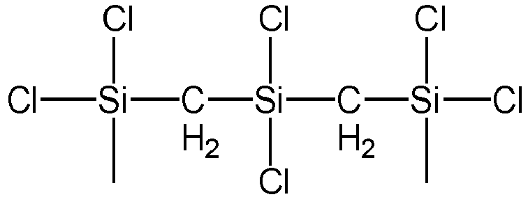


- In another aspect, there is provided a method for depositing a film selected from a carbon-doped silicon oxide film and a carbon-doped silicon oxynitride film onto at least a surface of a substrate comprising:
- placing the substrate into a reactor;
- heating the reactor to one or more temperatures ranging from about 25°C to about 550°C;
- introducing into the reactor a precursor comprising at least one compound selected from a silicon precursor listed in Table 1 and 2 and combinations thereof;
- introducing into the reactor a nitrogen source to react with at least a portion of the precursor to form a carbon doped silicon nitride film; and
- treating the carbon doped silicon nitride film with an oxygen source at one or more temperatures ranging from about 25°C to 1000°C or from about 100° to 400°C under conditions sufficient to convert the carbon doped silicon nitride film into the film. In certain embodiments, the carbon doped silicon oxide film or the carbon doped silicon oxynitride film has a carbon content of about 10 atomic weight percent (at. %) or greater as measured by XPS and an etch rate of at least 0.5 times less than thermal silicon oxide as measured in dilute hydrofluoric acid.
- If desired, the invention further comprises treating the carbon doped silicon containing film with hydrogen or hydrogen/inert plasma at 25°C to 600°C.
- One aspect of the invention relates to a composition comprising:
- (a) at least one linear or cyclic silicon precursor compound having one Si-C-Si or two Si-C-Si linkages selected from the group consisting of 1,1,1,3,3,3-hexachloro-1,3-disilapropane, 1,1,1,3,3,3-hexachloro-2-methyl-1,3-disilapropane, 1,1,1,3,3,3-hexachloro-2,2-dimethyl-1,3-disilapropane, 1,1,1,3,3,3-hexachloro-2-ethyl-1,3-disilapropane, 1-chloro-1,3-disilacyclobutane, 1-bromo-1,3-disilacyclobutane, 1,3-dichloro-1,3-1,3-disilacyclobutane, 1,3-dibromo-1,3-disilacyclobutane, 1,1,3-trichloro-1,3-disilacyclobutane, 1,1,3-tribromo-1,3-disilacyclobutane, 1,1,3,3-tetrachloro-1,3-disilacyclobutane, 1,1,3,3-tetrabromo-1,3-disilacyclobutane, 1,3-dichloro-1,3-dimethyl-1,3-disilacyclobutane, 1,3-bromo-1,3-dimethyl-1,3-disilacyclobutane, 1,1,1,3,3,5,5,5-octachloro-1,3,5-trisilapentane, 1,1,1,3,3,5,5,5-octachloro-1,3,5-trisilapentane, 1,1,1,3,3,5,5,5-octachloro-1,5-dimethyl-1,3,5-trisilapentane, 1,1,1,5,5,5-hexachloro-3,3-dimethyl-1,3,5-trisilapentane, 1,1,3,5,5,5-pentachloro-1,3,5-trimethyl-1,3,5-trisilapentane, 1,1,1,5,5,5-hexachloro-1,3,5-trisilapentane, 1,1,5,5-tetraachloro-1,3,5-trisilapentane; and;
- (b) at least one solvent.
- Another aspect of the invention relates to a method for forming a carbon doped silicon oxide film having carbon content ranging from 15 at % to 30 at.% via a thermal ALD process, the method comprising:
- a) placing one or more substrates comprising a surface feature into a reactor;
- b) heating to reactor to one or more temperatures ranging from ambient temperature to about 550°C and optionally maintaining the reactor at a pressure of 100 torr or less;
- c) introducing into the reactor at least one silicon precursor having two Si-C-Si linkages selected from the group consisting of 1-chloro-1,3-disilacyclobutane, 1-bromo-1,3-disilacyclobutane, 1,3-dichloro-1,3-1,3-disilacyclobutane, 1,3-dibromo-1,3-disilacyclobutane, 1,1,3-trichloro-1,3-disilacyclobutane, 1,1,3-tribromo-1,3-disilacyclobutane, 1,1,3,3-tetrachloro-1,3-disilacyclobutane, 1,1,3,3-tetrabromo-1,3-disilacyclobutane, 1,3-dichloro-1,3-dimethyl-1,3-disilacyclobutane, 1,3-bromo-1,3-dimethyl-1,3-disilacyclobutane, 1,1,1,3,3,5,5,5-octachloro-1,3,5-trisilapentane, 1,1,1,3,3,5,5,5-octachloro-1,3,5-trisilapentane, 1,1,1,3,3,5,5,5-octachloro-1,5-dimethyl-1,3,5-trisilapentane, 1,1,1,5,5,5-hexachloro-3,3-dimethyl-1,3,5-trisilapentane, 1,1,3,5,5,5-pentachloro-1,3,5-trimethyl-1,3,5-trisilapentane, 1,1,1,5,5,5-hexachloro-1,3,5-trisilapentane, 1,1,5,5-tetraachloro-1,3,5-trisilapentane;
- d) purge with an inert gas;
- e) providing a nitrogen source into the reactor to react with the surface to form a carbon doped silicon nitride film;
- f) purge with inert gas to remove reaction by-products
- g) steps c to f are repeated to provide a desired thickness of carbon doped silicon nitride;
- h) treating the resulting carbon doped silicon nitride film with an oxygen source at one or more temperatures ranging from about ambient temperature to 1000°C or from about 100° to 400°C to convert the carbon doped silicon nitride film into a carbon doped silicon oxide film; and
- i) providing post-deposition exposing the carbon doped silicon oxide film to a plasma comprising hydrogen.
- In one aspect of the invention, the substrate comprises silicon or germanium doped silicon or boron doped silicon or high k material and subsequent to depositing the inventive carbon doped silicon oxide film, a film comprising silicon nitride or silicon oxide is deposited.
- A further aspect of the invention relates to a film having a k of less than about 4, a carbon content of at least about 10 at. %, preferably 15 at. % or greater, most preferably 20 at. % or greater based on XPS measurement and, in another aspect the inventive film can be formed according to any of the inventive methods. Since the carbon content is an important factor for reducing the wet etch rate as well as increasing the ash resistance, the carbon content for this invention ranges from 10 at. % to 40 at. %, preferably 15 at. % to 30 at. %, and most preferably 20 at. % to 35 at. % as measured by XPS.
- Another aspect of the invention relates to stainless steel container housing the inventive compositions.
- The embodiments of the invention may be used alone or in various combinations with each other.
-
Figure 1 Etching profile comparison for 1,1,1,3,3,3-hexachloro-1,3-disilapropane (HCDSP) and 1,1,3,3-tetrachloro-1,3-disilacyclobutane (TCDSB) carbon doped silicon oxide film after plasma treatment followed by oxygen ash, demonstrating carbon doped silicon oxide film from TCDSB provides more ash resistance than that of HCDSP. - Described herein are silicon precursor compounds, and compositions and methods comprising same, to deposit a carbon doped (e.g., having a carbon content of about 10 at. % or greater as measured by XPS) silicon-containing film via a deposition process such as, without limitation, a thermal atomic layer deposition process. The film deposited using the composition and method described herein exhibits an extremely low etch rate such as an etch rate of at least 0.5 times less than thermal silicon oxide as measured in dilute hydrofluoric acid (e.g., about 0.20 Å/s or less or about 0.15 Å/s or less in dilute HF (0.5 wt. %), or an etch rate of at least 0.1 times less than thermal silicon oxide, or an etch rate of at least 0.05 times less than thermal silicon oxide, or an etch rate of at least 0.01 times less than thermal silicon oxide while exhibiting variability in other tunable properties such as, without limitation, density, dielectric constant, refractive index, and elemental composition.
- In certain embodiments, the silicon precursor precursors described herein, and methods using same, impart one or more of the following features in the following manner. First, the as-deposited, reactive carbon-doped silicon nitride film is formed using the silicon precursor precursors comprising a Si-C-Si linkage, and a nitrogen source. Without wishing to be bound by any theory or explanation, it is believed that the Si-C-Si linkage from the silicon precursor remains in the resulting as-deposited film and provides a high carbon content of at least 10 at. % or greater as measured by XPS (e.g., about 20 to about 30 at. %, about 10 to about 20 at. % and in some cases about 10 to about 15 at. % carbon). Second, when exposing the as-deposited film to an oxygen source, such as water, either intermittently during the deposition process, as a post-deposition treatment, or a combination thereof, at least a portion or all of the nitrogen content in the film is converted to oxygen to provide a film selected from a carbon-doped silicon oxide or a carbon-doped silicon oxynitride film. The nitrogen in the as-deposited film is released as one or more nitrogen-containing by-products such as ammonia or an amine group.
- In this or other embodiments, the final film is porous and has a density of about 1.7 grams/cubic centimeter (g/cc) or less and an etch rate of 0.20 Å/s or less in 0.5 wt. % dilute hydrogen fluoride.
- In one aspect, the composition for depositing a silicon-containing film comprises: (a) at least one silicon precursor compound having one Si-C-Si or two Si-C-Si linkages selected from the group consisting of 1,1,1,3,3,3-hexachloro-1,3-disilapropane, 1,1,1,3,3,3-hexachloro-2-methyl-1,3-disilapropane, 1,1,1,3,3,3-hexachloro-2,2-dimethyl-1,3-disilapropane, 1,1,1,3,3,3-hexachloro-2-ethyl-1,3-disilapropane, 1-chloro-1,3-disilacyclobutane, 1-bromo-1,3-disilacyclobutane, 1,3-dichloro-1,3-1,3-disilacyclobutane, 1,3-dibromo-1,3-disilacyclobutane, 1,1,3-trichloro-1,3-disilacyclobutane, 1,1,3-tribromo-1,3-disilacyclobutane, 1,1,3,3-tetrachloro-1,3-disilacyclobutane, 1,1,3,3-tetrabromo-1,3-disilacyclobutane, 1,3-dichloro-1,3-dimethyl-1,3-disilacyclobutane, 1,3-bromo-1,3-dimethyl-1,3-disilacyclobutane, 1,1,1,3,3,5,5,5-octachloro-1,3,5-trisilapentane, 1,1,1,3,3,5,5,5-octachloro-1,3,5-trisilapentane, 1,1,1,3,3,5,5,5-octachloro-1,5-dimethyl-1,3,5-trisilapentane, 1,1,1,5,5,5-hexachloro-3,3-dimethyl-1,3,5-trisilapentane, 1,1,3,5,5,5-pentachloro-1,3,5-trimethyl-1,3,5-trisilapentane, 1,1,1,5,5,5-hexachloro-1,3,5-trisilapentane, 1,1,5,5-tetraachloro-1,3,5-trisilapentane; and; (b) at least one solvent. In certain embodiments of the composition described herein, exemplary solvents can include, without limitation, ether, tertiary amine, alkyl hydrocarbon, aromatic hydrocarbon, tertiary aminoether, siloxanes, and combinations thereof. In certain embodiments, the difference between the boiling point of the compound having one Si-C-Si or two Si-C-Si linkages and the boiling point of the solvent is 40°C or less. The wt % of silicon precursor compound in the solvent can vary from 1 to 99 wt %, or 10 to 90 wt%, or 20 to 80 wt %, or 30 to 70 wt %, or 40 to 60 wt %, to 50 to 50 wt %. In some embodiments, the composition can be delivered via direct liquid injection into a reactor chamber for silicon-containing film using conventional direct liquid injection equipment and methods.
- In one embodiment of the method described herein, the carbon doped silicon oxide film having carbon content ranging from 5 at. % to 20 at. % is deposited using a thermal ALD process and a plasma comprising hydrogen to improve film properties. In this embodiment, the method comprises:
- a. placing one or more substrates comprising a surface feature into a reactor;
- b. heating to reactor to one or more temperatures ranging from ambient temperature to about 550°C and optionally maintaining the reactor at a pressure of 100 torr or less;
- c. introducing into the reactor at least one silicon precursor having one Si-C-Si linkage selected from the group consisting of 1,1,1,3,3,3-hexachloro-1,3-disilapropane, 1,1,1,3,3,3-hexachloro-2-methyl-1,3-disilapropane, 1,1,1,3,3,3-hexachloro-2,2-dimethyl-1,3-disilapropane, 1,1,1,3,3,3-hexachloro-2-ethyl-1,3-disilapropane;
- d. purge with an inert gas thereby removing unreacted silicon precursor and forming a composition comprising the purge gas and silicon precursor;
- e. providing a nitrogen source into the reactor to react with the surface to form a silicon carbonitride films;
- f. purge with inert gas to remove reaction by-products;
- g. steps c to f are repeated to provide a desired thickness of carbon doped silicon nitride;
- h. providing post-deposition treating the carbon doped silicon nitride film with an oxygen source at one or more temperatures ranging from about ambient temperature to 1000°C or from about 100° to 400°C to convert the carbon doped silicon nitride film into a carbon doped silicon oxide film either in situ or in another chamber; and
- i. providing post-deposition exposing the carbon doped silicon oxide film to a plasma comprising hydrogen to improve film properties to improve at least one of the films' properties;
- j. optionally post-deposition treating the carbon doped silicon oxide film with a spike anneal at temperatures from 400° to 1000°C or a UV light source. In this or other embodiments, the UV exposure step can be carried out either during film deposition, or once deposition has been completed.
- In one embodiment, the substrate includes at least one feature wherein the feature comprises a pattern trench with aspect ratio of 1:9, opening of 180 nm.
- In an embodiment of the method described herein, the carbon doped silicon oxide film having carbon content ranging from 15 at. % to 30 at.% is deposited using a thermal ALD process and a plasma comprising hydrogen to improve film properties. In this embodiment, the method comprises:
- a. placing one or more substrates comprising a surface feature into a reactor (e.g., into a conventional ALD reactor);
- b. heating to reactor to one or more temperatures ranging from ambient temperature to about 550°C and optionally maintaining the reactor at a pressure of 100 torr or less;
- c. introducing into the reactor at least one silicon precursor having two Si-C-Si linkages selected from the group consisting of 1-chloro-1,3-disilacyclobutane, 1-bromo-1,3-disilacyclobutane, 1,3-dichloro-1,3-1,3-disilacyclobutane, 1,3-dibromo-1,3-disilacyclobutane, 1,1,3-trichloro-1,3-disilacyclobutane, 1,1,3-tribromo-1,3-disilacyclobutane, 1,1,3,3-tetrachloro-1,3-disilacyclobutane, 1,1,3,3-tetrabromo-1,3-disilacyclobutane, 1,3-dichloro-1,3-dimethyl-1,3-disilacyclobutane, 1,3-bromo-1,3-dimethyl-1,3-disilacyclobutane, 1,1,1,3,3,5,5,5-octachloro-1,3,5-trisilapentane, 1,1,1,3,3,5,5,5-octachloro-1,3,5-trisilapentane, 1,1,1,3,3,5,5,5-octachloro-1,5-dimethyl-1,3,5-trisilapentane, 1,1,1,5,5,5-hexachloro-3,3-dimethyl-1,3,5-trisilapentane, 1,1,3,5,5,5-pentachloro-1,3,5-trimethyl-1,3,5-trisilapentane, 1,1,1,5,5,5-hexachloro-1,3,5-trisilapentane, 1,1,5,5-tetraachloro-1,3,5-trisilapentane;
- d. purge with an inert gas;
- e. providing a nitrogen source into the reactor to react with the surface to form a carbon doped silicon nitride film;
- f. purge with inert gas to remove reaction by-products;
- g. steps c to f are repeated to provide a desired thickness of carbon doped silicon nitride;
- h. providing post-deposition treating the carbon doped silicon nitride film with an oxygen source at one or more temperatures ranging from about ambient temperature to 1000°C or from about 100° to 400°C to convert the carbon doped silicon nitride film into a carbon doped silicon oxide film either in situ or in another chamber;
- i. providing post-deposition exposing the carbon doped silicon oxide film to a plasma comprising hydrogen to improve at least one of the films' physical properties.
- j. optionally post-deposition treating the carbon doped silicon oxide film with a thermal anneal at temperatures from 400° to 1000°C or a UV light source. In this or other embodiments, the UV exposure step can be carried out either during film deposition, or once deposition has been completed.
- In yet another further embodiment of the method described herein, the silicon containing film is deposited using a thermal ALD process with a catalyst comprising an ammonia or organic amine. In this embodiment, the method comprises:
- a. placing one or more substrates comprising a surface feature into a reactor;
- b. heating the reactor to one or more temperatures ranging from ambient temperature to about 150°C and optionally maintaining the reactor at a pressure of 100 torr or less;
- c. introducing into the reactor at least one silicon precursor having one or two Si-C-Si linkages selected from the group consisting of 1,1,1,3,3,3-hexachloro-1,3-disilapropane, 1,1,1,3,3,3-hexachloro-2-methyl-1,3-disilapropane, 1,1,1,3,3,3-hexachloro-2,2-dimethyl-1,3-disilapropane, 1,1,1,3,3,3-hexachloro-2-ethyl-1,3-disilapropane, 1-chloro-1,3-disilacyclobutane, 1-bromo-1,3-disilacyclobutane, 1,3-dichloro-1,3-1,3-disilacyclobutane, 1,3-dibromo-1,3-disilacyclobutane, 1,1,3-trichloro-1,3-disilacyclobutane, 1,1,3-tribromo-1,3-disilacyclobutane, 1,1,3,3-tetrachloro-1,3-disilacyclobutane, 1,1,3,3-tetrabromo-1,3-disilacyclobutane, 1,3-dichloro-1,3-dimethyl-1,3-disilacyclobutane, 1,3-bromo-1,3-dimethyl-1,3-disilacyclobutane, 1,1,1,3,3,5,5,5-octachloro-1,3,5-trisilapentane, 1,1,1,3,3,5,5,5-octachloro-1,3,5-trisilapentane, 1,1,1,3,3,5,5,5-octachloro-1,5-dimethyl-1,3,5-trisilapentane, 1,1,1,5,5,5-hexachloro-3,3-dimethyl-1,3,5-trisilapentane, 1,1,3,5,5,5-pentachloro-1,3,5-trimethyl-1,3,5-trisilapentane, 1,1,1,5,5,5-hexachloro-1,3,5-trisilapentane, 1,1,5,5-tetraachloro-1,3,5-trisilapentane and a catalyst;
- d. purge with an inert gas
- e. providing vapors of water into the reactor to react with the precursor as well as a catalyst to form a carbon doped silicon oxide as-deposited film;
- f. purge with inert gas to remove reaction by-products;
- g. steps c to f are repeated to provide a desired thickness of carbon doped silicon oxide;
- h. providing post-deposition exposing the processed film to a plasma comprising hydrogen to improve film properties to improve at least one of the films' properties;
- i. optionally post-deposition treating the carbon doped silicon oxide film with a spike anneal at temperatures from 400° to 1000°C or a UV light source. In this or other embodiments, the UV exposure step can be carried out either during film deposition, or once deposition has been completed.
- In this or other embodiments, the catalyst is selected from a Lewis base such as pyridine, piperazine, ammonia, triethylamine or other organic amines. The amount of Lewis base vapors is at least one equivalent to the amount of the silicon precursor vapors during step c.
- In certain embodiments, the resulting carbon doped silicon oxide film is exposed to organoaminosilanes or chlorosilanes having Si-Me or Si-H or both to form a hydrophobic thin layer before exposing to hydrogen plasma treatment. Suitable organoaminosilanes include, but not limited to, diethylaminotrimethylsilane, dimethylaminotrimethylsilane, ethylmethylaminotrimethylsilane, t-butylaminotrimethylsilane, iso-propylaminotrimethylsilane, di-isopropylaminotrimethylsilane, pyrrolidinotrimethylsilane, diethylaminodimethylsilane, dimethylaminodimethylsilane, ethylmethylaminodimethylsilane, t-butylaminodimethylsilane, iso-propylaminodimethylsilane, di-isopropylaminodimethylsilane, pyrrolidinodimethylsilane, bis(diethylamino)dimethylsilane, bis(dimethylamino)dimethylsilane, bis(ethylmethylamino)dimethylsilane, bis(di-isopropyllamino)dimethylsilane, bis(isopropylamino)dimethylsilane, bis(tert-butylamino)dimethylsilane, dipyrrolidinodimethylsilane, bis(diethylamino)diethylsilane, bis(diethylamino)methylvinylsilane, bis(dimethylamino)methylvinylsilane bis(ethylmethylamino)methylvinylsilane, bis(diisopropyllamino)methylvinylsilane, bis(iso-propylamino)methylvinylsilane, bis(tert-butylamino)methylvinylsilane, dipyrrolidinomethylvinylsilane, 2,6-dimethylpiperidinomethylsilane, 2,6-dimethylpiperidinodimethylsilane, 2,6-dimethylpiperidinotrimethylsilane, tris(dimethylamino)phenylsilane, tris(dimethylamino)methylsilane, di-iso-propylaminosilane, di-sec-butylaminosilane, chlorodimethylsilane, chlorotrimethylsilane, dichloromethylsilane, and dichlorodimethylsilane.
- In another embodiments, the resulting carbon doped silicon oxide film is exposed to alkoxysilanes or cyclic alkoxysilanes having Si-Me or Si-H or both to form a hydrophobic thin layer before exposing to hydrogen plasma treatment. Suitable alkoxysilanes or cyclic alkoxysilanes include, but not limited to, diethoxymethylsilane, dimethoxymethylsilane, diethoxydmethylsilane, dimethoxydmethylsilane, 2,4,6,8-Tetramethylcyclotetrasiloxane, or octamethylcyclotetrasiloxane. Without wishing to be bound by any theory or explanation, it is believed that the thin layer formed by the organoaminosilanes or alkoxysilanes or cyclic alkoxysilanes may convert into dense carbon doped silicon oxide during plasma ashing process, further boosting the ashing resistance.
- In another embodiment, a vessel for depositing a silicon-containing film comprising one or more silicon precursor compounds described herein. In one particular embodiment, the vessel comprises at least one pressurizable vessel (preferably of stainless steel having a design such as disclosed in U.S. Patent Nos.
US7334595 ;US6077356 ;US5069244 ; andUS5465766 the disclosure of which is hereby incorporated by reference. The container can comprise either glass (borosilicate or quartz glass) or type 316, 316L, 304 or 304L stainless steel alloys (UNS designation S31600, S31603, S30400 S30403) fitted with the proper valves and fittings to allow the delivery of one or more precursors to the reactor for a CVD or an ALD process. In this or other embodiments, the silicon precursor is provided in a pressurizable vessel comprised of stainless steel and the purity of the precursor is 98% by weight or greater or 99.5% or greater which is suitable for the semiconductor applications. The silicon precursor compounds are preferably substantially free of metal ions such as, Al3+ ions, Fe2+, Fe3+, Ni2+, Cr3+. As used herein, the term "substantially free" as it relates to Al3+ ions, Fe2+, Fe3+, Ni2+, Cr3+ means less than about 5 ppm (by weight), preferably less than about 3 ppm, and more preferably less than about 1 ppm, and most preferably about 0.1 ppm. In certain embodiments, such vessels can also have means for mixing the precursors with one or more additional precursor if desired. In these or other embodiments, the contents of the vessel(s) can be premixed with an additional precursor. Alternatively, the silicon precursor is and/or other precursor can be maintained in separate vessels or in a single vessel having separation means for maintaining the silicon precursor is and other precursor separate during storage. - The silicon-containing film is deposited upon at least a surface of a substrate such as a semiconductor substrate. In the method described herein, the substrate may be comprised of and/or coated with a variety of materials well known in the art including films of silicon such as crystalline silicon or amorphous silicon, silicon oxide, silicon nitride, amorphous carbon, silicon oxycarbide, silicon oxynitride, silicon carbide, germanium, germanium doped silicon, boron doped silicon, metal such as copper, tungsten, aluminum, cobalt, nickel, tantalum), metal nitride such as titanium nitride, tantalum nitride, metal oxide, group III/V metals or metalloids such as GaAs, InP, GaP and GaN, and a combination thereof. These coatings may completely coat the semi-conductor substrate, may be in multiple layers of various materials and may be partially etched to expose underlying layers of material. The surface may also have on it a photoresist material that has been exposed with a pattern and developed to partially coat the substrate. In certain embodiments, the semiconductor substrate comprising at least one surface feature selected from the group consisting of pores, vias, trenches, and combinations thereof. The potential application of the silicon-containing films include but not limited to low k spacer for FinFET or nanosheet, sacrificial hard mask for self aligned patterning process (such as SADP, SAQP, or SAOP).
- The deposition method used to form the silicon-containing films or coatings are deposition processes. Examples of suitable deposition processes for the method disclosed herein include, but are not limited to, a chemical vapor deposition or an atomic layer deposition process. As used herein, the term "chemical vapor deposition processes" refers to any process wherein a substrate is exposed to one or more volatile precursors, which react and/or decompose on the substrate surface to produce the desired deposition. As used herein, the term "atomic layer deposition process" refers to a self-limiting (e.g., the amount of film material deposited in each reaction cycle is constant), sequential surface chemistry that deposits films of materials onto substrates of varying compositions. As used herein, the term "thermal atomic layer deposition process" refers to atomic layer deposition process at substrate temperatures ranging from room temperature to 600°C without in situ or remote plasma. Although the precursors, reagents and sources used herein may be sometimes described as "gaseous", it is understood that the precursors can be either liquid or solid which are transported with or without an inert gas into the reactor via direct vaporization, bubbling or sublimation. In some case, the vaporized precursors can pass through a plasma generator.
- In one embodiment, the silicon-containing film is deposited using an ALD process. In another embodiment, the silicon-containing film is deposited using a CCVD process. In a further embodiment, the silicon-containing film is deposited using a thermal ALD process. The term "reactor" as used herein, includes without limitation, reaction chamber or deposition chamber.
- In certain embodiments, the method disclosed herein avoids pre-reaction of precursor(s) by using ALD or CCVD methods that separate the precursor(s) prior to and/or during the introduction to the reactor. In this connection, deposition techniques such as ALD or CCVD processes are used to deposit the silicon-containing film. In one embodiment, the film is deposited via an ALD process in a typical single wafer ALD reactor, semi-batch ALD reactor, or batch furnace ALD reactor by exposing the substrate surface alternatively to the one or more the silicon-containing precursor, oxygen source, nitrogen-containing source, or other precursor or reagent. Film growth proceeds by self-limiting control of surface reaction, the pulse length of each precursor or reagent, and the deposition temperature. However, once the surface of the substrate is saturated, the film growth ceases. In another embodiment, each reactant including the silicon precursor and reactive gas is exposed to a substrate by moving or rotating the substrate to different sections of the reactor and each section is separated by inert gas curtain, i.e. spatial ALD reactor or roll to roll ALD reactor.
- Depending upon the deposition method, in certain embodiments, the silicon precursors described herein and optionally other silicon-containing precursors may be introduced into the reactor at a predetermined molar volume, or from about 0.1 to about 1000 micromoles. In this or other embodiments, the precursor may be introduced into the reactor for a predetermined time period. In certain embodiments, the time period ranges from about 0.001 to about 500 seconds.
- In certain embodiments, the silicon-containing films deposited using the methods described herein are formed in the presence of a catalyst in combination with an oxygen source, reagent or precursor comprising oxygen, i.e. water vapors. An oxygen source may be introduced into the reactor in the form of at least one oxygen source and/or may be present incidentally in the other precursors used in the deposition process. Suitable oxygen source gases may include, for example, water (H2O) (e.g., deionized water, purified water, distilled water, water vapor, water vapor plasma, oxygenated water, air, a composition comprising water and other organic liquid), oxygen (02), oxygen plasma, ozone (03), nitric oxide (NO), nitrogen dioxide (NO2), carbon monoxide (CO), a plasma comprising water, a plasma comprising water and argon, hydrogen peroxide, a composition comprising hydrogen, a composition comprising hydrogen and oxygen, carbon dioxide (CO2), air, and combinations thereof. In certain embodiments, the oxygen source comprises an oxygen source gas that is introduced into the reactor at a flow rate ranging from about 1 to about 10000 square cubic centimeters (sccm) or from about 1 to about 1000 sccm. The oxygen source can be introduced for a time that ranges from about 0.1 to about 100 seconds. The catalyst is selected from a Lewis base such as pyridine, piperazine, trimethylamine, tert-butylamine, diethylamine, trimethylamine, ethylenediamine, ammonia, or other organic amines.
- In embodiments wherein the film is deposited by an ALD or a cyclic CVD process, the precursor pulse can have a pulse duration that is greater than 0.01 seconds, and the oxygen source can have a pulse duration that is less than 0.01 seconds, while the water pulse duration can have a pulse duration that is less than 0.01 seconds.
- In certain embodiments, the oxygen source is continuously flowing into the reactor while precursor pulse and plasma are introduced in sequence. The precursor pulse can have a pulse duration greater than 0.01 seconds while the plasma duration can range between 0.01 seconds to 100 seconds.
- In certain embodiments, the silicon-containing films comprise silicon and nitrogen. In these embodiments, the silicon-containing films deposited using the methods described herein are formed in the presence of nitrogen-containing source. A nitrogen-containing source may be introduced into the reactor in the form of at least one nitrogen source and/or may be present incidentally in the other precursors used in the deposition process.
- Suitable nitrogen-containing or nitrogen source gases may include, for example, ammonia, hydrazine, monoalkylhydrazine, symmetrical or unsymmetrical dialkylhydrazine, organoamines such as methylamine, ethylamine, ethylenediamine, ethanolamine, piperazine, N,N'-dimethylethylenediamine, imidazolidine, cyclotrimethylenetriamine, and combination thereof.
- In certain embodiments, the nitrogen source is introduced into the reactor at a flow rate ranging from about 1 to about 10000 square cubic centimeters (sccm) or from about 1 to about 1000 sccm. The nitrogen-containing source can be introduced for a time that ranges from about 0.1 to about 100 seconds. In embodiments wherein the film is deposited by an ALD or a cyclic CVD process using both a nitrogen and oxygen source, the precursor pulse can have a pulse duration that is greater than 0.01 seconds, and the nitrogen source can have a pulse duration that is less than 0.01 seconds, while the water pulse duration can have a pulse duration that is less than 0.01 seconds. In yet another embodiment, the purge duration between the pulses that can be as low as 0 seconds or is continuously pulsed without a purge in-between.
- The deposition methods disclosed herein may involve one or more purge gases. The purge gas, which is used to purge away unconsumed reactants and/or reaction byproducts, is an inert gas that does not react with the precursors. Exemplary purge gases include, but are not limited to, argon (Ar), nitrogen (N2), helium (He), neon, hydrogen (H2), and combinations thereof. In certain embodiments, a purge gas such as Ar is supplied into the reactor at a flow rate ranging from about 10 to about 10000 sccm for about 0.1 to 1000 seconds, thereby purging the unreacted material and any byproduct that may remain in the reactor.
- The respective step of supplying the precursors, oxygen source, the nitrogen-containing source, and/or other precursors, source gases, and/or reagents may be performed by changing the time for supplying them to change the stoichiometric composition of the resulting film.
- Energy is applied to the at least one of the precursor, nitrogen-containing source, reducing agent, other precursors or combination thereof to induce reaction and to form the film or coating on the substrate. Such energy can be provided by, but not limited to, thermal, plasma, pulsed plasma, helicon plasma, high density plasma, inductively coupled plasma, X-ray, e-beam, photon, remote plasma methods, and combinations thereof.
- In certain embodiments, a secondary RF frequency source can be used to modify the plasma characteristics at the substrate surface. In embodiments wherein the deposition involves plasma, the plasma-generated process may comprise a direct plasma-generated process in which plasma is directly generated in the reactor, or alternatively a remote plasma-generated process in which plasma is generated outside of the reactor and supplied into the reactor.
- Throughout the description, the term "ALD or ALD-like" refers to a process including, but not limited to, the following processes: a) each reactant including silicon precursor and reactive gas is introduced sequentially into a reactor such as a single wafer ALD reactor, semi-batch ALD reactor, or batch furnace ALD reactor; b) each reactant including silicon precursor and reactive gas is exposed to a substrate by moving or rotating the substrate to different sections of the reactor and each section is separated by inert gas curtain, i.e. spatial ALD reactor or roll to roll ALD reactor.
- The silicon precursors and/or other silicon-containing precursors may be delivered to the reaction chamber, such as a CVD or ALD reactor, in a variety of ways. In one embodiment, a liquid delivery system may be utilized. In an alternative embodiment, a combined liquid delivery and flash vaporization process unit may be employed, such as, for example, the turbo vaporizer manufactured by MSP Corporation of Shoreview, MN, to enable low volatility materials to be volumetrically delivered, which leads to reproducible transport and deposition without thermal decomposition of the precursor. In liquid delivery formulations, the precursors described herein may be delivered in neat liquid form, or alternatively, may be employed in solvent formulations or compositions comprising same. Thus, in certain embodiments the precursor formulations may include solvent component(s) of suitable character as may be desirable and advantageous in a given end use application to form a film on a substrate.
- In this or other embodiments, it is understood that the steps of the methods described herein may be performed in a variety of orders, may be performed sequentially or concurrently (e.g., during at least a portion of another step), and any combination thereof. The respective step of supplying the precursors and the nitrogen-containing source gases may be performed by varying the duration of the time for supplying them to change the stoichiometric composition of the resulting silicon-containing film.
- In a still further embodiment of the method described herein, the film or the as-deposited film is subjected to a treatment step. The treatment step can be conducted during at least a portion of the deposition step, after the deposition step, and combinations thereof. Exemplary treatment steps include, without limitation, treatment via high temperature thermal annealing; plasma treatment; ultraviolet (UV) light treatment; laser; electron beam treatment and combinations thereof to affect one or more properties of the film. The films deposited with the silicon precursors having one or two Si-C-Si linkages described herein, when compared to films deposited with previously disclosed silicon precursors under the same conditions, have improved properties such as, without limitation, a wet etch rate that is lower than the wet etch rate of the film before the treatment step or a density that is higher than the density prior to the treatment step. In one particular embodiment, during the deposition process, as-deposited films are intermittently treated. These intermittent or middeposition treatments can be performed, for example, after each ALD cycle, after a certain number of ALD, such as, without limitation, one (1) ALD cycle, two (2) ALD cycles, five (5) ALD cycles, or after every ten (10) or more ALD cycles.
- In an embodiment wherein the film is treated with a high temperature annealing step, the annealing temperature is at least 100°C or greater than the deposition temperature. In this or other embodiments, the annealing temperature ranges from about 400°C to about 1000°C. In this or other embodiments, the annealing treatment can be conducted in a vacuum (< 760 Torr), inert environment or in oxygen containing environment (such as H2O, N2O, NO2 or O2)
- In an embodiment wherein the film is treated to UV treatment, film is exposed to broad band UV or, alternatively, an UV source having a wavelength ranging from about 150 nanometers (nm) to about 400 nm. In one particular embodiment, the as-deposited film is exposed to UV in a different chamber than the deposition chamber after a desired film thickness is reached.
- In an embodiment where in the film is treated with a plasma, passivation layer such as SiOz or carbon doped SiOz is deposited to prevent chlorine and nitrogen contamination from penetrating film in the subsequent plasma treatment. The passivation layer can be deposited using atomic layer deposition or cyclic chemical vapor deposition.
- In an embodiment wherein the film is treated with a plasma, the plasma source is selected from the group consisting of hydrogen plasma, plasma comprising hydrogen and helium, plasma comprising hydrogen and argon. Hydrogen plasma lowers film dielectric constant and boost the damage resistance to following plasma ashing process while still keeping the carbon content in the bulk almost unchanged.
- Throughout the description, the term "ALD or ALD-like" refers to a process including, but not limited to, the following processes: a) each reactant including silicon precursor and reactive gas is introduced sequentially into a reactor such as a single wafer ALD reactor, semi-batch ALD reactor, or batch furnace ALD reactor; b) each reactant including silicon precursor and reactive gas is exposed to a substrate by moving or rotating the substrate to different sections of the reactor and each section is separated by inert gas curtain, i.e. spatial ALD reactor or roll to roll ALD reactor.
- Throughout the description, the term "ashing" refers to a process to remove the photoresist or carbon hard mask in semiconductor manufacturing process using a plasma comprising oxygen source such as O2/inert gas plasma, O2 plasma, CO2 plasma, CO plasma, H2/O2 plasma or combination thereof.
- Throughout the description, the term "damage resistance" refers to film properties after oxygen ashing process. Good or high damage resistance is defined as the following film properties after oxygen ashing: film dielectric constant lower than 4.5; carbon content in the bulk (at more than 50 Å deep into film) is within 5 at. % as before ashing; Less than 50 Å of the film is damaged, observed by differences in dilute HF etch rate between films near surface (less than 50 Å deep) and bulk (more than 50 Å deep).
- Throughout the description, the term "alkyl hydrocarbon" refers a linear or branched C1 to C20 hydrocarbon, cyclic C6 to C20 hydrocarbon. Exemplary hydrocarbon includes, but not limited to, heptane, octane, nonane, decane, dodecane, cyclooctane, cyclononane, cyclodecane.
- Throughout the description, the term "aromatic hydrocarbon" refers a C6 to C20 aromatic hydrocarbon. Exemplary aromatic hydrocarbon n includes, but not limited to, toluene, mesitylene.
- Throughout the description, the term "catalyst" refers a Lewis base in vapor phase which can catalyze surface reaction between hydroxyl group and Si-CI bond during thermal ALD process. Exemplary catalysts include, but not limited to, at least one of a cyclic amine-based gas such as aminopyridine, picoline, lutidine, piperazine, piperidine, pyridine or an organic amine-based gas methylamine, dimethylamine, trimethylamine, ethylamine, diethylamine, triethylamine, propylamine, iso-propylamine, di-propylamine, di-iso-propylamine, tert-butylamine.
- Throughout the description, the term "organic amines" refers a primary amine, secondary amine, tertiary amine having C1 to C20 hydrocarbon, cyclic C6 to C20 hydrocarbon. Exemplary organic amines include, but not limited to, methylamine, dimethylamine, trimethylamine, ethylamine, diethylamine, triethylamine, propylamine, iso-propylamine, di-propylamine, di-iso-propylamine, tert-butylamine.
- Throughout the description, the term "siloxanes" refer a linear, branched, or cyclic liquid compound having at least one Si-O-Si linkages and C4 to C20 carbon atoms. Exemplary siloxanes includes, but not limited to, tetramethyldisiloxane, hexamethyldisiloxane (HMDSO), 1,1,1,3,3,5,5,5-octamethyltrisiloxane, octamethylcyclotetrasiloxane (OMCTS).
- Throughout the description, the term "step coverage" as used herein is defined as a percentage of two thicknesses of the deposited film in a structured or featured substrate having either vias or trenches or both, with bottom step coverage being the ratio (in %): thickness at the bottom of the feature is divided by thickness at the top of the feature, and middle step coverage being the ratio (in %): thickness on a sidewall of the feature is divided by thickness at the top of the feature. Films deposited using the method described herein exhibit a step coverage of about 80% or greater, or about 90% or greater which indicates that the films are conformal.
- The following examples illustrate certain aspects of the instant invention and do not limit the scope of the appended claims.
- Film depositions were performed in a lab scale atomic layer deposition (ALD) reactor using a silicon precursor and ammonia as nitrogen source ammonia. The ALD cycle steps and process conditions are provided in the following Table 3:
Table 3: ALD Cycle Steps and Process Conditions Steps Descriptions Time Notes 1 Insert Si substrates into a reactor 2 Heat substrates to desired temperature ∼1-2 hours T = 300-500°C 3 Close throttle valve 2 seconds (s) Throttle valve is closed to increase residence time 4 Deliver silicon precursor dose 2 s Vapor draw; vapor pressure is 14-18 Torr 5 Deliver silicon precursor dose 2 s 6 Deliver silicon precursor dose 2 s After 3 doses of Si precursor, 7 Open throttle valve 2 s 8 Flow N2 to purge the reactor 6 s N2 flow is 5 Ipm 9 Evacuate the reactor to base pressure 6 s Base pressure is <1 mTorr 10 Flow NH3 24 s Pressure is set to 5 Torr; NH3 flow is 100 sccm 9 Flow N2 to purge the reactor 6 s N2 flow is 5 Ipm 10 Evacuate the reactor to base pressure 6 s Base pressure is <1 mTorr 11 Remove Si sample from the reactor - During the deposition, steps 3 to 10 are repeated for a number of cycles of up to 2000 times to get a desired thickness of the as-deposited carbon doped silicon nitride films. The resulting as-deposited films were subjected to either an in-situ (annealing performed inside the reactor on the as-deposited film) or ex-situ annealing (annealing outside or in a separate chamber) to convert into the films into a carbon doped silicon oxide films. Typical annealing conditions performed were as follows: moisture annealing was performed under vacuum at 30 Torr; air annealing was performed on a hot plate at ambient temperature (e.g., 25°C) or about 300 °C.
- Standard hydrogen containing plasma were used to treat a carbon doped silicon oxide film. The H2 plasma treatment parameters are:
- a. H2 only plasma:
- Plasma frequency = 13.56 MHz
- H2 flow = 135 sccm
- Chamber pressure = 2 Torr
- Time = 5 minutes
- b. H2/Ar plasma
- Plasma frequency = 13.56 MHz
- H2 flow = 65 sccm
- Ar flow = 65 sccm
- Chamber pressure = 2 Torr
- Time = 5 minutes
- Refractive index and thickness were measured directly after deposition using an ellipsometer at 632.8 nm. Bulk film composition was characterized using X-Ray Photoelectron Spectroscopy (XPS) at few nanometer (2-5 nm) down from the surface inorder to eliminate effect of adventitious carbon. Film density was characterized using X-Ray Reflectometry (XRR).
- Wet etch rate process was performed under two different concentration of dilute hydrofluoric acid (dHF), 1:199 49% HF and DI water as well as 1:99 49% HF and DI water). The more dilute HF concentration increases measurement accuracy for damaged layer. During the process, a thermal silicon oxide film was etched at the same time used to ensure etch solution consistency.
- Oxygen ashing process was performed at room temperature using commercial plasma asher PVA TePLA M4L. The process parameters are as follow: power = 100 - 200W; He/O2 = 1:3; pressure = 600 mTorr. Film dielectric constant (k) is calculated from C-V curve measured using MDC 802b Mercury Probe connected to HP4284 LCR meter. Measurement was done in a front-contact mode, which liquid metal (mercury) was used to form two electrically conductive contacts.
- Carbon doped silicon oxide film was deposited using thermal ALD process using 1,1,3,3-tetrachlorodisilacyclobutane (TCDSB) and 1,1,1,3,3,3-hexachloro-1,3-disilapropane (HCDSP) and ammonia at 300 °C as described in Table 3.
After deposition the film was then further treated ex-situ for 3 hours at 300 °C in air.Table 4. Film composition for carbon doped silicon oxide film deposited from 1,1,3,3-tetrachloro-1,3-disilcyclobutane and ammonia followed by annealing measured by XPS Si precursor C N O Si Cl 1,1,1,3,3,3-hexachloro-1,3-disilapropane (HCDSP) 9.5% 1.1% 56.8% 32.6% ND 1,1,3,3-tetrachlorodisilacyclobutane (TCDSB) 27.5% 1.2% 39.2% 40.3% ND - Table 4. shows film composition comparison between film deposited from HCDSP and TCDSB. The TCDSB film has a relatively large carbon content compared to HCDSP, demonstrating TCDSM is a better silicon precursor to introduce more carbon than HCDSP.
- The dHF etch rate for thermal silicon oxide reference etch rate is 0.48 ± 0.02 Å/s. the etch rate for HCDSP and TCDSB films are 0.10 Å/s and < 0.02 Å/s consecutively.
- The TDCSB film etch rate is below detection, limit of our measurement. Lower TDCSB film dilute HF etch rate (>5x lower) is consistent with higher carbon content in the film.
- Film dielectric constant for either carbon doped silicon oxide film deposited from HCDSP or TCDSB are greater than 5.
- The resulted carbon doped silicon oxide film deposited from HCDSP or TCDSB films were further treated with hydrogen plasma using 300 mm commercial PEALD tool using H2/Ar plasma using the conditions as aforementioned. Both HCDSP and TCDSB film have dielectric constant reduced to 3.5 and 3.4 respectively after plasma treatment, demonstrating plasma comprising hydrogen is an effective way to reduce dielectric constant.
- The films were then exposed to standard oxygen ash followed by dilute HF dip to determine damage. Referring now to
Figure 1, Figure 1 shows film thickness removed as function of time when dipping in dilute HF. - Both HCDSP and TCDSB films shows fast etch rate in the beginning before slowing down, indicating surface damage from oxygen ash. Oxygen ash oxidizes carbon from the film, hence, causing fast etch rate. Etch rate profile suggests damaged layer of 27 Å for TCDSB film and 39 Å for HCDSP film, suggesting TCDSB film is more oxygen ash resistance than HCDSP film under the same etching conditions.
- Carbon doped silicon oxide film on pattern structure was deposited from 1,1,3,3-tetrachloro-1,3-disilacyclobutane and ammonia at 300 °C as described in Table 3 followed by ex-situ treatment to 300 °C for 3 hours in air environment.
- Scanning electron microscope (SEM) was performed on the trench structure with aspect ratio of 1:9 and trench opening of 180 nm.
Table 5. Surface coverage of carbon doped silicon oxide film deposited from 1,1,3,3-tetrachloro-1,3-disilacyclobutane Top ¼ from top Middle ¾ from top Bottom Thickness (Å) 456 Å 476 Å 473 Å 456 Å 476 Å - The step coverage, shown in Table 5, for carbon doped silicon oxide film deposited from 1,1,3,3-tetrachloro-1,3-disilacyclobutane is > 99%.
- Silicon-containing films were deposited from 1,1,3,3-tetrachloro-1,3-disilacyclobutane and ammonia at substrate temperature of 500°C using the process steps described in Table 3 and stored in ambient.
- Film properties such as XPS and wet etch rate in dilute HF were obtained approximately a week after film deposition. The results of these tests are provided in Table 6.
Table 6. Film composition and WER of ALD films Temperature (°C) %O %N %C %CI %Si dHF WER relative to thermal oxide 500 20.1 18.1 23.9 0.4 37.6 0.12 - Referring to Table 6, the XPS data shows that the carbon doped silicon oxide had little chlorine content (e.g., less than 0.5 at.%). The film deposited at 500°C is has more nitrogen content compared to 300 °C while maintaining similar amount of carbon in the film. It is believed that at the lower deposition temperature of 300°C, the process may provide more Si-NH2 or Si-NH-Si fragments that are susceptible to oxidation. Deposition at the higher 500°C temperature, on the other hand, may provide enough energy to form a stronger Si-Nx network which is more resistant to oxidation.
- Carbon doped silicon oxide film was deposited using 1,1,3,3-tetrachloro-1,3-disilacyclobutane and ammonia at 300 °C as described in Table 3. In-situ H2O vapor treatment was performed on the film using the following parameters:
- H2O vapor draw; H2O canister temperature = 50 °C; Chamber pressure = 30 Torr; T = 300 °C.
- Film growth per cycle was 0.48 Å/cycle. The resulting film has refractive index of 1.55 and density of 1.55 g/cc. The film composition measured by XPS is O = 39.0%, N = 2.6%, C = 25.1% and Si = 33.2%. No chlorine detected in the film.
- Carbon doped silicon oxide film was deposited using 1,1,3,3-tetrachloro-1,3-disilacyclobutane and ammonia at 300 °C as described in Table 3 followed by thermal treatment at 300 °C in air. The carbon doped silicon oxide film was further heated in nitrogen at 200-400 °C, 5 Torr, for 1 hour prior to H2/Ar plasma treatment described previously.
- The film was then exposed to oxygen ash followed by dilute HF etch to determine damaged thickness.
- Film dielectric constant is shown in Table 7 while O2 ash damaged thickness are shown in Table 8.
Table 7. Dielectric constant of carbon doped silicon oxide film by H2/Ar plasma treatment. Dielectric constant after H2/Ar plasma treatment (before O2 ash) H2/Ar plasma treatment only 3.6 200 °C anneal before H2/Ar plasma treatment 2.8 300 °C anneal before H2/Ar plasma treatment 2.8 400 °C anneal before H2/Ar plasma treatment 3.2 Table 8. Damaged thickness of carbon doped silicon oxide film after exposed to O2 ash. Damaged thickness after O2 ash (Å) H2/Ar plasma treatment only 30 200 °C anneal before H2/Ar plasma treatment 32 300 °C anneal before H2/Ar plasma treatment 27 400 °C anneal before H2/Ar plasma treatment 31 - Additional annealing prior to H2/Ar plasma treatment shows lower dielectric constant (k = 2.8 - 3.2) over sample only treated with H2/Ar plasma (k = 3.6). The film has oxygen ash damaged thickness of 27 - 32 Å.
- Carbon doped silicon oxide film was deposited using 1,1,3,3-tetrachloro-1,3-disilacyclobutane as the silicon precursor and ammonia at 300 °C in ALD mode using 300mm commercial cross flow reactor. The ALD steps 2 to 8, shown in Table 9, are repeated to get desired thickness.
Table 9. ALD steps of carbon doped silicon oxide film deposition Steps Descriptions Time Notes 1 Insert Si substrates into a reactor 2 Heat substrates to desired temperature 30 minutes T = 300 °C 3 Flow the silicon precursor 1 seconds (s) Vapor draw; vapor pressure is 14-18 Torr Inner chamber Ar = 300 sccm, 8 Torr; Outer chamber Ar = 500 sccm, 7.5 Torr 4 Soak Si precursor 3 s Ar gas and precursor flow is stopped. Throttle valve close while maintaining chambers pressure. 5 Flow Ar to purge precursor 10 s Inner chamber Ar = 300 sccm, 8 Torr; Outer chamber Ar = 500 sccm, 7.5 Torr 6 Flow NH3 25 s NH3 = 100 sccm Inner chamber Ar = 300 sccm, 8 Torr; Outer chamber Ar = 500 sccm, 7.5 Torr 7 Flow Ar to purge precursor 10 s Inner chamber Ar = 300 sccm, 8 Torr; Outer chamber Ar = 500 sccm, 7.5 Torr 8 Remove Si sample from the reactor - The as-deposited sample was left in ambient convert into carbon doped silicon oxide film. The growth per cycle (GPC) of the films are 0.45 Å/cycle.
- The carbon doped silicon oxide film was further treated at 300 °C under nitrogen atmosphere for 1 hour followed by hydrogen-containing plasma treatment (either H2 only plasma or H2/Ar plasma) as described previously.
- After plasma treatment, the film was exposed to O2 ash followed by dilute HF to determine damaged thickness. The dielectric constant and damaged thickness after O2 ash are shown in Table 10.
Table 10. Dielectric constant of carbon doped silicon oxide film and damaged thickness after O2 ash Treatment Before treatment dielectric constant (k) After plasma (before O2 ash) dielectric constant (k) After O2 ash and dHF etch dielectric constant (k) O2 ash damaged thickness (Å) H2 only plasma 5.7 3.5 3.5 33 Å H2/Ar plasma 5.7 2.8 3.2 31 Å - The process demonstrated carbon doped silicon oxide film with high oxygen resistance and low-k before and after oxygen ash process. High oxygen resistance indicates by low damage thickness as well as low k after oxygen ash (k < 4.0)
- Carbon doped silicon oxide film was deposited using 1,1,3,3-tetrachloro-1,3-disilacyclobutane and ammonia at 300 °C in ALD mode using 300 mm commercial cross flow reactor followed by H2/Ar plasma as described in Example 6. The substrate used was patterned wafer with aspect ratio of 1:9 and opening of 180 nm.
- Transmission Electron Microscope (TEM) was used to determine surface coverage. Table 11 shows film thickness at various locations in the structure.
Table 11. Thickness of carbon doped silicon oxide deposited from 1,1,3,3-tetrachloro-1,3-disilacyclobutane followed by H2/Ar plasma treatment Top ¼ from top Middle ¾ from top Bottom 355 Å 353 Å 360 Å 362 Å 345 Å - The carbon doped silicon oxide film deposited from 1,1,3,3-tetrachloro-1,3-disilacyclobutane and ammonia at 300 °C as described in Table 9 was annealed at 300 °C in inert for 1 hour followed by exposure to chemical treatment using diethylaminotrimethylsilane. The chemical treatment parameters are:
T = 300 °C; Time = 5 min and 25 min; Chamber Pressure = 1 Torr - As control, the film was annealed only at 300 °C without any chemical exposure.
- After treatment, film dielectric constant is measured and shown in Table 12.
Table 12. Film dielectric constant after diethylaminotrimethylsilane treatment Temperature (°C) Time (minutes) Dielectric constant (k) No chemical treatment, anneal only at 300 °C 25 5.5 300 5 2.9 300 25 2.7 - The chemical treatment shows improvement in film dielectric constant, from 5.5 to less than 3.0.
- A solution of 20 wt. % of 1,1,3,3-tetrachloro-1,3-disilacyclobutane in octane was used for film deposition. The chemical was delivered using direct liquid injection (canister temperature = 60 °C, Ar flow through the vaporizer was 100 sccm. Liquid flow rate was ~200 mg/min). Vaporizer temperature was 70°C.
- The deposition process comprised of the following steps:
Table 13. Steps used to deposit silicon containing film using 1,1,3,3-tetrachloro-1,3-disilacyclobutane solution Steps Descriptions Time Notes 1 Insert Si substrates into a reactor 2 Heat substrates to desired temperature 5 minutes T = 300 °C 3 Flow 1,1,3,3-tetrachloro-1,3- disilacyclobutane 20% in octane2 seconds Ch P=8∼10Torr 4 Soak Si precursor 5 s Ar gas and precursor flow were stopped. Throttle valve closed while maintaining chambers pressure. 5 Flow Ar to purge precursor 10 s 6 Flow NH3 15 s NH3 = 500 sccm, Chamber pressure = 15Torr 7 Soak NH3 20 s NH3 flow stopped. Throttle valve closed 8 Flow Ar to purge NH3 10 s 9 Flow H2O vapor 1 hour 300 °C, chamber pressure = ∼30 Torr 10 Remove Si substrate from the reactor - Steps 3 to 4 were repeated 5 times before moving to step 5, and steps 3 to 8 were repeated multiple times to get desired thickness. Film composition analyzed by XPS are Si = 35.7%; O = 36.5%; C = 23.0%; N = 4.5%; Cl = 0.3%.
- The deposited film was further annealed in inert environment at 300 °C for 1 hour followed by H2/Ar plasma treatment.
- Treated films were exposed to standard O2 ash and dipped into dilute HF to determine damaged thickness. The damaged thickness after Oz ash are 38 Å and 37 Å for film treated with H2 only plasma and H2/Ar plasma consecutively.
- A solution of 20 wt. % of 1,1,3,3-tetrachloro-1,3-disilacyclobutane in octane was used for film deposition. The chemical was delivered using direct liquid injection (canister temperature = 60 °C, Ar flow through the vaporizer was 100 sccm. Liquid flow rate was ~200 mg/min). Vaporizer temperature was 70 °C.
- The deposition process comprised of the following steps:
Table 14. Steps used to deposit silicon containing film using 1,1,3,3-tetrachloro-1,3-disilacyclobutane solution Steps Descriptions Time Notes 1 Insert Si substrates into a reactor 2 Heat substrates to desired temperature 5 minutes T = 300 °C 3 Flow 1,1,3,3-tetrachloro-1,3-disilacyclobutane and pyridine, co-injection 0.5 second Chamber pressure = 5 Torr Precursor temperature = 70 °C, Ar carrier gas = 25 sccm Nitrogen for pressure control = 200 sccm Ar for pressure control = 50 sccm 4 Flow inert gas to purge unreacted precursors 15s Nitrogen = 200 sccm Ar = 50 sccm 5 Flow H2O and pyridine, co-injection 3 s Chamber pressure = 5 Torr Water pressure = 17 Torr Nitrogen for pressure control = 200 sccm Ar for pressure control = 50 sccm 6 Flow inert gas for purging 15s Nitrogen = 200 sccm Argon = 50 sccm 7 Flow H2O vapor 1 hour 300 °C, chamber pressure = ∼30Torr 8 Flow N2 for drying 30 min 300 - 500 °C, chamber pressure = 5 Torr 9 Turn on H2 only plasma 5 min H2 = 200 sccm; Freq = 13.56 MHz, chamber pressure = 2 Torr; power = 100 W 10 Remove Si film from the reactor - Steps 3 to 4 were repeated 5 times before moving to step 5, and steps 3 to 6 were repeated multiple times to get desired thickness.
Step 8,9, and 10 are optional for comparison.Table 15. Film properties of carbon doped silicon oxide film processed in-situ using 1,1,3,3-tetrachloro-1,3-disilacyclobutane. WER (Å/s) Density (g/cc) Si at. % O at. % C at. % N at. % Cl at. % No additional process 0.08 1.34 36.04 33.17 28.69 0.6 1.5 N2 dry <0.02 1.44 36.19 34.37 27.33 0.3 1.8 N2 dry + H2 plasma <0.02 1.58 36.39 35.43 25.68 0.54 1.9 - The resulting film has film properties in Table 15. Film etch rates are very low, i.e. 0.12x thermal oxide, for as-deposited film with no anneal. The etch rates dropped to level below our detection limit after additional processing (N2 dry or N2 dry and plasma).
- Film density for as-deposited film is 1.34 g/cc with slight densification with additional N2 dry or N2 dry and H2 plasma treatment. In all cases, the film has high carbon content 25-29% and low Cl content (< 2%).
- 1,1,3,3-tetrachloro-1,3-disilacyclobutane and H2O were used for film deposition. Pyridine was used as a reaction catalyst. The chemical (canister temp = 70°C) was delivered with Ar sweeping through the precursor canister. Water temperature was 17 °C (vapor pressure = 15 torr) and water vapor was delivered with vapor draw, and pyridine temp was 25~35 °C (vapor pressure= 15~25 torr) and pyridine vapor was delivered with vapor draw. Main N2 flow rate was 200 sccm, and Ar flow rate was 50 sccm.
- The deposition process comprised of the steps described in Table 16.
Table 16. Deposition steps used in depositing Si-containing film from 1,1,3,3-tetrachloro-1,3-disilacyclobutane and water/pyridine. Steps Descriptions Time Notes 1 Insert Si substrates into a reactor 2 Heat substrates to desired temperature 5 minutes T = 40 °C 3 Flow 1,1,3,3-tetrachloro-1,3-disilacyclobutane and pyridine, co-injection 0.5 second Chamber pressure = 5 Torr Precursor temperature = 70 °C, Ar carrier gas = 25 sccm Nitrogen for pressure control = 200 sccm Ar for pressure control = 50 sccm 4 Flow inert gas to purge unreacted precursors 15s Nitrogen = 200 sccm Ar = 50 sccm 5 Flow H2O and pyridine, co-injection 3s Chamber pressure = 5 Torr Water pressure = 17 Torr Nitrogen for pressure control = 200 sccm Ar for pressure control = 50 sccm 6 Flow inert gas for purging 15s Nitrogen = 200 sccm Argon = 50 sccm 7 Remove Si substrate from the reactor - Steps 3 to 6 were repeated 500 times to get desired thickness.
- The film as-deposited has refractive index of 1.53 and GPC of 0.8 Å/cycle. The film composition, measured by XPS, is: Si = 35.3%, O = 34.0%, C = 28.9%, N = 0.6% and Cl = 1.3%. Film density is 1.8 g/cc and dilute etch rate is 0.08 Å/s.
- The film then subjected to standard ex-situ H2/Ar plasma treatment at 300 °C as described previously. The film dielectric constant was measured before and after plasma treatment is 3.6, which is improved from as-deposited film (k = 6.1)
- A solution of 20 wt. % of 1,1,3,3-tetrachloro-1,3-disilacyclobutane in octane was used for film deposition. The chemical was delivered using direct liquid injection (canister temperature = 60 °C, Ar flow through the vaporizer was 100 sccm. Liquid flow rate was ~200 mg/min). Vaporizer temperature was 70°C.
- The deposition process comprised of the steps described in Table 17.
Table 17. Deposition steps used in depositing silicon containing film using 1,1,3,3-tetrachloro-1,3-disilacyclobutane solution Steps Descriptions Time Notes 1 Insert Si substrates into a reactor 2 Heat substrates to desired temperature 5 minutes T = 300 °C 3 Flow 1,1,3,3-tetrachloro-1,3- disilacyclobutane 20% in octane2 seconds Ch P=8 Torr 4 Soak Si precursor 5s Ar gas and precursor flow were stopped. Throttle valve closed while maintaining chambers pressure. 5 Flow Ar to purge precursor 10s 6 Flow NH3 15s NH3 = 500 sccm, Chamber pressure = 15Torr 7 Soak NH3 20 s NH3 flow stopped. Throttle valve closed 8 Flow Ar to purge NH3 10s 9 Flow H2O vapor to convert to SiO2 1 hour 300 °C, chamber pressure = 5 Torr 10 Remove Si film from the reactor - Steps 3 to 4 were repeated 5 times before moving to step 5, and steps 3 to 8 were repeated multiple times to get desired thickness. The Step 9 is optional for some wafers in order to get comparison between H2O in-situ anneal and conversion in ambient.
- Table 18 shows similar film composition as measured by XPS, for both carbon doped silicon oxide converted in ambient and the one with in-situ H2O treatment.
Table 18. Comparison of Film Composition of Carbon Doped Silicon Oxide Si O C N Cl Ambient conversion 34.69 41.4 21.82 1.74 0.35 In-situ H2O 35.2 38.22 23.49 2.82 0.27 - Carbon doped silicon oxide film was deposited using 1,1,3,3-tetrachloro-1,3-disilacyclobutane and ammonia at 300 °C in ALD mode using 300 mm commercial cross flow reactor. The ALD steps, shown in Table 8, are repeated to get desired thickness.
- The as-deposited carbon doped silicon oxide film was annealed at 500 °C to 800 °C in inert for 1 hour.
- The film dielectric constant shows in Table 19.
Table 19. Dielectric constant of Si-containing film, deposited using 1,1,3,3-tetrachloro-1,3-disilacyclobutane and ammonia, after thermal annealing Annealing temperature (°C) dielectric constant (k) after annealing (before oxygen ash) No anneal (room temperature) 5.7 500 °C 2.6 600 °C 2.3 700 °C 2.6 800 °C 3.9 - Carbon doped silicon oxide film was deposited using diethoxymethylsilane (DEMS) using a 200 mm commercial PECVD tool at 300 °C. The process parameters are as follow: Power = 500W; Pressure = 9 Torr; Si precursor flow = 500 sccm; He flow = 300 sccm; film thickness = 500 Å.
- The as-deposited film has composition shown in Table 20
Table 20. Film composition of Carbon doped silicon oxide film using DEMS PECVD process, measured by XPS Measurement depth (Å) C% N O Si Cl 0 21.8% ND 44.8% 27.0 % ND 100 28.3% ND 46.4% 32.7% ND - The film density is 1.48 g/cc. WER in dilute HF (1:99 49% HF and DI water) for as-deposited (before H2 plasma) is in Table 21. The film shows very high dilute HF etch resistance, indicating by low etch rate.
Table 21. WER in dilute HF (1:99, 0.5 wt.%) for Carbon doped silicon oxide from as-deposited PECVD DEMS (before H2 plasma). The thermal silicon oxide reference etch rate is 0.48 ± 0.02 Å/s Etch time (seconds) Carbon doped silicon oxide film Thickness (Å) Etch rate (Å/s) 0 515 N/A 15 513 0.16 195 512 0.03 - The film was then treated with H2 plasma for 5 minutes at 300 W and 300 °C. After H2 plasma treatment, the sample was exposed to oxygen ashing. Both hydrogen plasma treatment and oxygen ashing processes are the same as described previously.
- Table 22 shows dielectric constant measurement of PECVD DEMS samples
Table 22. PECVD DEMS dielectric constant after H2 plasma treatment and H2 plasma followed by oxygen ashing Dielectric constant (k) Before H2 plasma 5 min H2 plasma After 5 min H2 plasma and oxygen ashing PECVD DEMS 3.2 3.7 5.5 - The dielectric constant increases after H2 plasma from 3.2 to 3.7 indicating higher damaged thickness. Oxygen ashing further increases film dielectric constant to 5.5. The dilute HF (1:99 49% HF and DI water) characterization after H2 plasma followed by oxygen ashing, tabulated in Table 17.
Table 23. WER in dilute HF (1:99) for carbon doped silicon oxide from PECVD DEMS after H2 plasma followed by oxygen ashing ash. The thermal silicon oxide reference etch rate is 0.48 ± 0.02 Å/s Etch time (seconds) Carbon doped silicon oxide film Thickness (Å) Etch rate (Å/s) 0 484 N/A 15 435 3.29 195 377 0.32 - The Carbon doped silicon oxide film clearly shows damaged layer thickness more than 100 Å. Film etch rate for film after oxygen ash is much higher than (> 10x) as deposited film. High film dielectric constant after exposing to oxygen ashing process is consistent with thick damaged layer from oxygen ash.
- Carbon doped silicon oxide film was deposited using thermal ALD process using 1,1,3,3-tetrachloro-1,3-disilacyclobutane and ammonia at 300 °C as described in Table 3. After deposition the film was then anneal at room temperature in air for 3 hours at 300 °C. Standard oxygen ash was performed on the carbon doped silicon oxide film. Dilute HF was used to determine damaged thickness, shown in Table 24.
Table 24. Dilute HF etch rate of carbon doped silicon oxide film after exposed to oxygen ash Etch time (seconds) Carbon doped silicon oxide film Thickness (Å) Etch rate (Å/s) 0 626 - 15 586 2.67 30 533 3.56 60 413 3.99 120 364 0.81 240 350 0.12 480 343 0.06 - The etch rate of the first ~260 Å from the surface shows very high etch rate compared to as deposited film (0.01 Å/s) suggest that carbon is removed. Carbon removal is consistent with damaged film from oxygen ash.
- Table 25 summarizes the solubility of 1,1,3,3-tetrachloro-1,3-disilacyclobutane in various solvents as potential formulation for delivery of vapors via direct liquid injection since 1,1,3,3-tetrachloro-1,3-disilacyclobutane is a solid at room temperature.
Solvent Solubility wt.% mol % (moles of 280/total moles) OMCTS 23.0 20.6 dodecane 26.2 18.3 HMDSO 30.5 24.0 octane 47.3 31.2 cyclooctane 51.2 34.2 toluene 57.7 35.7 - While the invention has been described with reference to certain embodiments, it will be understood by those skilled in the art that various changes may be made and equivalents may be substituted for elements thereof without departing from the scope of the invention. In addition, many modifications may be made to adapt a particular situation or material to the teachings of the invention without departing from the essential scope thereof. Therefore, it is intended that the invention not be limited to the particular embodiment disclosed as the best mode contemplated for carrying out this invention, but that the invention will include all embodiments falling within the scope of the appended claims.
- Aspects of the invention include:
- #1). A composition comprising:
- (a) at least one silicon precursor compound having one Si-C-Si or two Si-C-Si linkages selected from the group consisting of 1,1,1,3,3,3-hexachloro-1,3-disilapropane, 1,1,1,3,3,3-hexachloro-2-methyl-1,3-disilapropane, 1,1,1,3,3,3-hexachloro-2,2-dimethyl-1,3-disilapropane, 1,1,1,3,3,3-hexachloro-2-ethyl-1,3-disilapropane, 1-chloro-1,3-disilacyclobutane, 1-bromo-1,3-disilacyclobutane, 1,3-dichloro-1,3-1,3-disilacyclobutane, 1,3-dibromo-1,3-disilacyclobutane, 1,1,3-trichloro-1,3-disilacyclobutane, 1,1,3-tribromo-1,3-disilacyclobutane, , 1,1,3,3-tetrabromo-1,3-disilacyclobutane, 1,3-dichloro-1,3-dimethyl-1,3-disilacyclobutane, 1,3-bromo-1,3-dimethyl-1,3-disilacyclobutane, 1,1,1,3,3,5,5,5-octachloro-1,3,5-trisilapentane, 1,1,1,3,3,5,5,5-octachloro-1,3,5-trisilapentane, 1,1,1,3,3,5,5,5-octachloro-1,5-dimethyl-1,3,5-trisilapentane, 1,1,1,5,5,5-hexachloro-3,3-dimethyl-1,3,5-trisilapentane, 1,1,3,5,5,5-pentachloro-1,3,5-trimethyl-1,3,5-trisilapentane, 1,1,1,5,5,5-hexachloro-1,3,5-trisilapentane, 1,1,5,5-tetraachloro-1,3,5-trisilapentane; and;
- (b) at least one solvent.
- #2). The composition of #1 where in the solvent comprises at least one member selected from the group consisting of ether, tertiary amine, siloxanes, alkyl hydrocarbon, aromatic hydrocarbon, and tertiary aminoether.
- #3). The composition of #1 wherein the difference between the boiling point of the silicon precursor and the boiling point of the solvent is about 40°C or less.
- #4). The composition of #1 comprising less than 5ppm of at least one metal ions selected from the group consisting of Al3+ ions, Fe2+, Fe3+, Ni2+, and Cr3+.
- #5). The composition of #1 where in the solvent comprises at least one member selected from the group consisting of heptane, octane, nonane, decane, dodecane, cyclooctane, cyclononane, cyclodecane, toluene, and mesitylene.
- #6). A method for forming a carbon doped silicon oxide film having carbon content ranging from 15 at. % to 30 at.% via a thermal ALD process, the method comprising:
- placing one or more substrates comprising a surface feature into a reactor;
- heating to reactor to one or more temperatures ranging from ambient temperature to about 550°C and optionally maintaining the reactor at a pressure of 100 torr or less;
- introducing into the reactor at least one silicon precursor having two Si-C-Si linkages selected from the group consisting of 1-chloro-1,3-disilacyclobutane, 1-bromo-1,3-disilacyclobutane, 1,3-dichloro-1,3-1,3-disilacyclobutane, 1,3-dibromo-1,3-disilacyclobutane, 1,1,3-trichloro-1,3-disilacyclobutane, 1,1,3-tribromo-1,3-disilacyclobutane, 1,1,3,3-tetrachloro-1,3-disilacyclobutane, 1,1,3,3-tetrabromo-1,3-disilacyclobutane, 1,3-dichloro-1,3-dimethyl-1,3-disilacyclobutane, 1,3-bromo-1,3-dimethyl-1,3-disilacyclobutane, 1,1,1,3,3,5,5,5-octachloro-1,3,5-trisilapentane, 1,1,1,3,3,5,5,5-octachloro-1,3,5-trisilapentane, 1,1,1,3,3,5,5,5-octachloro-1,5-dimethyl-1,3,5-trisilapentane, 1,1,1,5,5,5-hexachloro-3,3-dimethyl-1,3,5-trisilapentane, 1,1,3,5,5,5-pentachloro-1,3,5-trimethyl-1,3,5-trisilapentane, 1,1,1,5,5,5-hexachloro-1,3,5-trisilapentane, 1,1,5,5-tetraachloro-1,3,5-trisilapentane;
- purge with an inert gas;
- providing a nitrogen source into the reactor to react with the surface to form a carbon doped silicon nitride film;
- purge with inert gas to remove reaction by-products;
- steps c to f are repeated to provide a desired thickness of carbon doped silicon nitride;
- treating the resulting carbon doped silicon nitride film with an oxygen source at one or more temperatures ranging from about ambient temperature to 1000oC or from about 100o to 400oC to convert the carbon doped silicon nitride film into a carbon doped silicon oxide film; and
- providing post-deposition exposing the carbon doped silicon oxide film to a plasma comprising hydrogen.
- #7) The method of #6 wherein the silicon precursor comprises the composition of #1.
- #8) A film formed according to the method of #6 having a k of less than about 4, a carbon content of at least about 10 at. %.
- #9) A film formed according to the method of #6 having an etch rate of at least 0.5 times less than thermal silicon oxide.
- #10) A film formed according to the method of #6 having an etch rate of at least 0.1 times less than thermal silicon oxide.
- #11) A film formed according to the method of #6 having an etch rate of at least 0.05 times less than thermal silicon oxide.
- #12) A film formed according to the method of #6 having an etch rate of at least 0.01 times less than thermal silicon oxide.
- #13) A film formed according to the method of #6 having less damage layer (50 Å or less) when exposing to oxygen ashing process.
- #14) A film formed according to the method of #6 having less damage layer (20 Å or less) when exposing to oxygen ashing process.
- #15) A film formed according to the method of #6 having less damage layer (10 Å or less) when exposing to oxygen ashing process.
- #16) A film formed according to the method of #6 having less damage layer (5 Å or less) when exposing to oxygen ashing process.
- #17) A stainless steel container housing the composition of #1.
- #18) A method for forming a carbon doped silicon oxide film having carbon content ranging from 15 at % to 30 at.% via a thermal ALD process, the method comprising the method comprising:
- placing one or more substrates comprising a surface feature into a reactor;
- heating the reactor to one or more temperatures ranging from ambient temperature to about 150°C and optionally maintaining the reactor at a pressure of 100 torr or less;
- introducing into the reactor at least precursor having two Si-C-Si linkages selected from the group consisting of 1-chloro-1,3-disilacyclobutane, 1-bromo-1,3-disilacyclobutane, 1,3-dichloro-1,3-1,3-disilacyclobutane, 1,3-dibromo-1,3-disilacyclobutane, 1,1,3-trichloro-1,3-disilacyclobutane, 1,1,3-tribromo-1,3-disilacyclobutane, 1,1,3,3-tetrachloro-1,3-disilacyclobutane, 1,1,3,3-tetrabromo-1,3-disilacyclobutane, 1,3-dichloro-1,3-dimethyl-1,3-disilacyclobutane, 1,3-bromo-1,3-dimethyl-1,3-disilacyclobutane, 1,1,1,3,3,5,5,5-octachloro-1,3,5-trisilapentane, 1,1,1,3,3,5,5,5-octachloro-1,3,5-trisilapentane, 1,1,1,3,3,5,5,5-octachloro-1,5-dimethyl-1,3,5-trisilapentane, 1,1,1,5,5,5-hexachloro-3,3-dimethyl-1,3,5-trisilapentane, 1,1,3,5,5,5-pentachloro-1,3,5-trimethyl-1,3,5-trisilapentane, 1,1,1,5,5,5-hexachloro-1,3,5-trisilapentane, 1,1,5,5-tetraachloro-1,3,5-trisilapentane and a catalyst;
- purge with an inert gas
- providing vapors of water into the reactor to react with the precursor as well as a catalyst to form a carbon doped silicon oxide as-deposited film;
- purge with inert gas to remove reaction by-products;
- steps c to f are repeated to provide a desired thickness of carbon doped silicon oxide;
- #19. The method of #18 further comprising post-deposition treatment of the carbon doped silicon oxide film with a thermal anneal at temperatures from 300 to 700°C.
- #20. The method of #18 further comprising hydrogen plasma treatment of the carbon doped silicon oxide film with a plasma comprising hydrogen.
Claims (13)
- A composition comprising:(a) at least one silicon precursor compound having one Si-C-Si or two Si-C-Si linkages selected from the group consisting of 1,1,1,3,3,3-hexachloro-1,3-disilapropane, 1,1,1,3,3,3-hexachloro-2-methyl-1,3-disilapropane, 1,1,1,3,3,3-hexachloro-2,2-dimethyl-1,3-disilapropane, 1,1,1,3,3,3-hexachloro-2-ethyl-1,3-disilapropane, 1-chloro-1,3-disilacyclobutane, 1-bromo-1,3-disilacyclobutane, 1,3-dichloro-1,3-1,3-disilacyclobutane, 1,3-dibromo-1,3-disilacyclobutane, 1,1,3-trichloro-1,3-disilacyclobutane, 1,1,3-tribromo-1,3-disilacyclobutane, , 1,1,3,3-tetrabromo-1,3-disilacyclobutane, 1,3-dichloro-1,3-dimethyl-1,3-disilacyclobutane, 1,3-bromo-1,3-dimethyl-1,3-disilacyclobutane, 1,1,1,3,3,5,5,5-octachloro-1,3,5-trisilapentane, 1,1,3,3,5,5-hexachloro-1,5-dimethyl-1,3,5-trisilapentane, 1,1,1,5,5,5-hexachloro-3,3-dimethyl-1,3,5-trisilapentane, 1,1,3,5,5,5-pentachloro-1,3,5-trimethyl-1,3,5-trisilapentane, 1,1,1,5,5,5-hexachloro-1,3,5-trisilapentane, 1,1,5,5-tetraachloro-1,3,5-trisilapentane; and;(b) at least one solvent.
- The composition of claim 1 wherein the silicon precursor compound having one SiC-Si or two Si-C-Si linkages is selected from the group consisting of 1,1,1,3,3,3-hexachloro-2-methyl-1,3-disilapropane, 1,1,1,3,3,3-hexachloro-2,2-dimethyl-1,3-disilapropane, 1,1,1,3,3,3-hexachloro-2-ethyl-1,3-disilapropane, 1,1,1,3,3,5,5,5-octachloro-1,3,5-trisilapentane, 1,1,3,3,5,5-hexachloro-1,5-dimethyl-1,3,5-trisilapentane, 1,1,1,5,5,5-hexachloro-3,3-dimethyl-1,3,5-trisilapentane, 1,1,1,5,5,5-hexachloro-1,3,5-trisilapentane, 1,1,5,5-tetrachloro-1,3,5-trisilapentane.
- The composition of claim 1 or claim 2 wherein the solvent comprises at least one member selected from the group consisting of ether, tertiary amine, siloxanes, alkyl hydrocarbon, aromatic hydrocarbon, and tertiary aminoether.
- The composition of claim 1 or claim 2 wherein the difference between the boiling point of the silicon precursor and the boiling point of the solvent is 40°C or less.
- The composition of claim 1 or claim 2 comprising less than 5ppm of at least one metal ions selected from the group consisting of Al3+ ions, Fe2+, Fe3+, Ni2+, and cr3+.
- The composition of claim 1 or claim 2 where in the solvent comprises at least one member selected from the group consisting of heptane, octane, nonane, decane, dodecane, cyclooctane, cyclononane, cyclodecane, toluene, and mesitylene.
- A method for depositing a carbon doped silicon oxide film using the composition of claim 1 or claim 2 via a thermal ALD process.
- A method according to claim 7 for forming a carbon doped silicon oxide film having carbon content ranging from 15 at. % to 30 at. % via a thermal ALD process, the method comprising:a) placing one or more substrates comprising a surface feature into a reactor;b) heating the reactor to one or more temperatures ranging from ambient temperature to 550°C and optionally maintaining the reactor at a pressure of 13.3 kPa (100 torr) or less;c) introducing into the reactor at least one silicon precursor having two Si-C-Si linkages selected from the group consisting of 1-chloro-1,3-disilacyclobutane, 1-bromo-1,3-disilacyclobutane, 1,3-dichloro-1,3-1,3-disilacyclobutane, 1,3-dibromo-1,3-disilacyclobutane, 1,1,3-trichloro-1,3-disilacyclobutane, 1,1,3-tribromo-1,3-disilacyclobutane, 1,1,3,3-tetrachloro-1,3-disilacyclobutane, 1,1,3,3-tetrabromo-1,3-disilacyclobutane, 1,3-dichloro-1,3-dimethyl-1,3-disilacyclobutane, 1,3-bromo-1,3-dimethyl-1,3-disilacyclobutane, 1,1,1,3,3,5,5,5-octachloro-1,3,5-trisilapentane, 1,1,3,3,5,5-hexachloro-1,5-dimethyl-1,3,5-trisilapentane, 1,1,1,5,5,5-hexachloro-3,3-dimethyl-1,3,5-trisilapentane, 1,1,3,5,5,5-pentachloro-1,3,5-trimethyl-1,3,5-trisilapentane, 1,1,1,5,5,5-hexachloro-1,3,5-trisilapentane, 1,1,5,5-tetraachloro-1,3,5-trisilapentane;d) purging with an inert gas;e) providing a nitrogen source into the reactor to react with the surface to form a carbon doped silicon nitride film;f) purging with inert gas to remove reaction by-products;g) repeating steps c to f to provide a desired thickness of carbon doped silicon nitride;h) treating the resulting carbon doped silicon nitride film with an oxygen source at one or more temperatures ranging from ambient temperature to 1000°C or from 100° to 400°C to convert the carbon doped silicon nitride film into a carbon doped silicon oxide film; andi) providing post-deposition exposing the carbon doped silicon oxide film to a plasma comprising hydrogen.
- The method of claim 8 wherein the silicon precursor comprises the composition of claim 1 or claim 2.
- A method according to claim 7 for forming a carbon doped silicon oxide film having carbon content ranging from 15 at. % to 30 at. % via a thermal ALD process, the method comprising the method comprising:a. placing one or more substrates comprising a surface feature into a reactor;b. heating the reactor to one or more temperatures ranging from ambient temperature to 150°C and optionally maintaining the reactor at a pressure of 13.3 kPa (100 torr) or less;c. introducing into the reactor at least a precursor having two Si-C-Si linkages selected from the group consisting of 1-chloro-1,3-disilacyclobutane, 1-bromo-1,3-disilacyclobutane, 1,3-dichloro-1,3-1,3-disilacyclobutane, 1,3-dibromo-1,3-disilacyclobutane, 1,1,3-trichloro-1,3-disilacyclobutane, 1,1,3-tribromo-1,3-disilacyclobutane, 1,1,3,3-tetrachloro-1,3-disilacyclobutane, 1,1,3,3-tetrabromo-1,3-disilacyclobutane, 1,3-dichloro-1,3-dimethyl-1,3-disilacyclobutane, 1,3-bromo-1,3-dimethyl-1,3-disilacyclobutane, 1,1,1,3,3,5,5,5-octachloro-1,3,5-trisilapentane, 1,1,3,3,5,5-hexachloro-1,5-dimethyl-1,3,5-trisilapentane, 1,1,1,5,5,5-hexachloro-3,3-dimethyl-1,3,5-trisilapentane, 1,1,3,5,5,5-pentachloro-1,3,5-trimethyl-1,3,5-trisilapentane, 1,1,1,5,5,5-hexachloro-1,3,5-trisilapentane,1,1,5,5-tetraachloro-1,3,5-trisilapentane and a catalyst;d. purging with an inert gase. providing vapors of water into the reactor to react with the precursor as well as a catalyst to form a carbon doped silicon oxide as-deposited film;f. purging with inert gas to remove reaction by-products;g. repeating steps c to f to provide a desired thickness of carbon doped silicon oxide.
- The method of claim 10 further comprising post-deposition treatment of the carbon doped silicon oxide film with a thermal anneal at temperatures from 300 to 700°C.
- The method of claim 10 further comprising hydrogen plasma treatment of the carbon doped silicon oxide film with a plasma comprising hydrogen.
- A method according to claim 7 for forming a carbon doped silicon oxide film having carbon content ranging from 5 at. % to 20 at. % via a thermal ALD process, the method comprising:a. placing one or more substrates comprising a surface feature into a reactor;b. heating the reactor to one or more temperatures ranging from ambient temperature to 550°C and optionally maintaining the reactor at a pressure of 13.3 kPa (100 torr) or less;c. introducing into the reactor at least one silicon precursor having one Si-C-Si linkage selected from the group consisting of 1,1,1,3,3,3-hexachloro-1,3-disilapropane, 1,1,1,3,3,3-hexachloro-2-methyl-1,3-disilapropane, 1,1,1,3,3,3-hexachloro-2,2-dimethyl-1,3-disilapropane, 1,1,1,3,3,3-hexachloro-2-ethyl-1,3-disilapropane;d. purging with an inert gas thereby removing unreacted silicon precursor and forming a composition comprising the purge gas and silicon precursor;e. providing a nitrogen source into the reactor to react with the surface to form a silicon carbonitride film;f. purging with inert gas to remove reaction by-products;g. repeating steps c to f to provide a desired thickness of carbon doped silicon nitride;h. treating the carbon doped silicon nitride film with an oxygen source at one or more temperatures ranging from ambient temperature to 1000°C or from 100° to 400°C to convert the carbon doped silicon nitride film into a carbon doped silicon oxide film either in situ or in another chamber; andi. providing post-deposition exposing the carbon doped silicon oxide film to a plasma comprising hydrogen; andj. optionally post-deposition treating the carbon doped silicon oxide film with a spike anneal at temperatures from 400° to 1000°C or a UV light source.
Applications Claiming Priority (4)
| Application Number | Priority Date | Filing Date | Title |
|---|---|---|---|
| US201662367260P | 2016-07-27 | 2016-07-27 | |
| US15/654,426 US20180033614A1 (en) | 2016-07-27 | 2017-07-19 | Compositions and Methods Using Same for Carbon Doped Silicon Containing Films |
| EP17835182.1A EP3491167B1 (en) | 2016-07-27 | 2017-07-26 | Compositions and methods using same for carbon doped silicon containing films |
| PCT/US2017/043890 WO2018022719A1 (en) | 2016-07-27 | 2017-07-26 | Compositions and methods using same for carbon doped silicon containing films |
Related Parent Applications (2)
| Application Number | Title | Priority Date | Filing Date |
|---|---|---|---|
| EP17835182.1A Division EP3491167B1 (en) | 2016-07-27 | 2017-07-26 | Compositions and methods using same for carbon doped silicon containing films |
| EP17835182.1A Division-Into EP3491167B1 (en) | 2016-07-27 | 2017-07-26 | Compositions and methods using same for carbon doped silicon containing films |
Publications (2)
| Publication Number | Publication Date |
|---|---|
| EP4253597A2 true EP4253597A2 (en) | 2023-10-04 |
| EP4253597A3 EP4253597A3 (en) | 2023-12-06 |
Family
ID=61011718
Family Applications (2)
| Application Number | Title | Priority Date | Filing Date |
|---|---|---|---|
| EP17835182.1A Active EP3491167B1 (en) | 2016-07-27 | 2017-07-26 | Compositions and methods using same for carbon doped silicon containing films |
| EP23187485.0A Pending EP4253597A3 (en) | 2016-07-27 | 2017-07-26 | Compositions and methods using same for carbon doped silicon containing films |
Family Applications Before (1)
| Application Number | Title | Priority Date | Filing Date |
|---|---|---|---|
| EP17835182.1A Active EP3491167B1 (en) | 2016-07-27 | 2017-07-26 | Compositions and methods using same for carbon doped silicon containing films |
Country Status (9)
| Country | Link |
|---|---|
| US (5) | US20180033614A1 (en) |
| EP (2) | EP3491167B1 (en) |
| JP (2) | JP6849788B2 (en) |
| KR (6) | KR102345918B1 (en) |
| CN (1) | CN109689928B (en) |
| IL (2) | IL291934B2 (en) |
| SG (1) | SG11201900319PA (en) |
| TW (3) | TWI720741B (en) |
| WO (1) | WO2018022719A1 (en) |
Families Citing this family (341)
| Publication number | Priority date | Publication date | Assignee | Title |
|---|---|---|---|---|
| US9394608B2 (en) | 2009-04-06 | 2016-07-19 | Asm America, Inc. | Semiconductor processing reactor and components thereof |
| US20130023129A1 (en) | 2011-07-20 | 2013-01-24 | Asm America, Inc. | Pressure transmitter for a semiconductor processing environment |
| US12334332B2 (en) | 2012-06-12 | 2025-06-17 | Lam Research Corporation | Remote plasma based deposition of silicon carbide films using silicon-containing and carbon-containing precursors |
| US10832904B2 (en) | 2012-06-12 | 2020-11-10 | Lam Research Corporation | Remote plasma based deposition of oxygen doped silicon carbide films |
| US10325773B2 (en) | 2012-06-12 | 2019-06-18 | Novellus Systems, Inc. | Conformal deposition of silicon carbide films |
| US9234276B2 (en) | 2013-05-31 | 2016-01-12 | Novellus Systems, Inc. | Method to obtain SiC class of films of desired composition and film properties |
| US20180347035A1 (en) | 2012-06-12 | 2018-12-06 | Lam Research Corporation | Conformal deposition of silicon carbide films using heterogeneous precursor interaction |
| US10714315B2 (en) | 2012-10-12 | 2020-07-14 | Asm Ip Holdings B.V. | Semiconductor reaction chamber showerhead |
| US20160376700A1 (en) | 2013-02-01 | 2016-12-29 | Asm Ip Holding B.V. | System for treatment of deposition reactor |
| US9564309B2 (en) | 2013-03-14 | 2017-02-07 | Asm Ip Holding B.V. | Si precursors for deposition of SiN at low temperatures |
| US11015245B2 (en) | 2014-03-19 | 2021-05-25 | Asm Ip Holding B.V. | Gas-phase reactor and system having exhaust plenum and components thereof |
| US10858737B2 (en) | 2014-07-28 | 2020-12-08 | Asm Ip Holding B.V. | Showerhead assembly and components thereof |
| US10941490B2 (en) | 2014-10-07 | 2021-03-09 | Asm Ip Holding B.V. | Multiple temperature range susceptor, assembly, reactor and system including the susceptor, and methods of using the same |
| SG11201703195QA (en) * | 2014-10-24 | 2017-05-30 | Versum Materials Us Llc | Compositions and methods using same for deposition of silicon-containing film |
| US10276355B2 (en) | 2015-03-12 | 2019-04-30 | Asm Ip Holding B.V. | Multi-zone reactor, system including the reactor, and method of using the same |
| US20160314964A1 (en) | 2015-04-21 | 2016-10-27 | Lam Research Corporation | Gap fill using carbon-based films |
| US10458018B2 (en) | 2015-06-26 | 2019-10-29 | Asm Ip Holding B.V. | Structures including metal carbide material, devices including the structures, and methods of forming same |
| US10410857B2 (en) | 2015-08-24 | 2019-09-10 | Asm Ip Holding B.V. | Formation of SiN thin films |
| US10211308B2 (en) | 2015-10-21 | 2019-02-19 | Asm Ip Holding B.V. | NbMC layers |
| US11139308B2 (en) | 2015-12-29 | 2021-10-05 | Asm Ip Holding B.V. | Atomic layer deposition of III-V compounds to form V-NAND devices |
| US10529554B2 (en) | 2016-02-19 | 2020-01-07 | Asm Ip Holding B.V. | Method for forming silicon nitride film selectively on sidewalls or flat surfaces of trenches |
| US10343920B2 (en) | 2016-03-18 | 2019-07-09 | Asm Ip Holding B.V. | Aligned carbon nanotubes |
| US10190213B2 (en) | 2016-04-21 | 2019-01-29 | Asm Ip Holding B.V. | Deposition of metal borides |
| US10367080B2 (en) | 2016-05-02 | 2019-07-30 | Asm Ip Holding B.V. | Method of forming a germanium oxynitride film |
| US11453943B2 (en) | 2016-05-25 | 2022-09-27 | Asm Ip Holding B.V. | Method for forming carbon-containing silicon/metal oxide or nitride film by ALD using silicon precursor and hydrocarbon precursor |
| US9859151B1 (en) | 2016-07-08 | 2018-01-02 | Asm Ip Holding B.V. | Selective film deposition method to form air gaps |
| US10612137B2 (en) | 2016-07-08 | 2020-04-07 | Asm Ip Holdings B.V. | Organic reactants for atomic layer deposition |
| US20180033614A1 (en) * | 2016-07-27 | 2018-02-01 | Versum Materials Us, Llc | Compositions and Methods Using Same for Carbon Doped Silicon Containing Films |
| KR102532607B1 (en) | 2016-07-28 | 2023-05-15 | 에이에스엠 아이피 홀딩 비.브이. | Substrate processing apparatus and method of operating the same |
| US9887082B1 (en) | 2016-07-28 | 2018-02-06 | Asm Ip Holding B.V. | Method and apparatus for filling a gap |
| US9812320B1 (en) | 2016-07-28 | 2017-11-07 | Asm Ip Holding B.V. | Method and apparatus for filling a gap |
| US10643826B2 (en) | 2016-10-26 | 2020-05-05 | Asm Ip Holdings B.V. | Methods for thermally calibrating reaction chambers |
| US11532757B2 (en) | 2016-10-27 | 2022-12-20 | Asm Ip Holding B.V. | Deposition of charge trapping layers |
| US10714350B2 (en) | 2016-11-01 | 2020-07-14 | ASM IP Holdings, B.V. | Methods for forming a transition metal niobium nitride film on a substrate by atomic layer deposition and related semiconductor device structures |
| KR102546317B1 (en) | 2016-11-15 | 2023-06-21 | 에이에스엠 아이피 홀딩 비.브이. | Gas supply unit and substrate processing apparatus including the same |
| US10002787B2 (en) * | 2016-11-23 | 2018-06-19 | Lam Research Corporation | Staircase encapsulation in 3D NAND fabrication |
| KR102762543B1 (en) | 2016-12-14 | 2025-02-05 | 에이에스엠 아이피 홀딩 비.브이. | Substrate processing apparatus |
| US11447861B2 (en) | 2016-12-15 | 2022-09-20 | Asm Ip Holding B.V. | Sequential infiltration synthesis apparatus and a method of forming a patterned structure |
| US11581186B2 (en) | 2016-12-15 | 2023-02-14 | Asm Ip Holding B.V. | Sequential infiltration synthesis apparatus |
| KR102700194B1 (en) | 2016-12-19 | 2024-08-28 | 에이에스엠 아이피 홀딩 비.브이. | Substrate processing apparatus |
| US10269558B2 (en) | 2016-12-22 | 2019-04-23 | Asm Ip Holding B.V. | Method of forming a structure on a substrate |
| US10867788B2 (en) | 2016-12-28 | 2020-12-15 | Asm Ip Holding B.V. | Method of forming a structure on a substrate |
| US11390950B2 (en) | 2017-01-10 | 2022-07-19 | Asm Ip Holding B.V. | Reactor system and method to reduce residue buildup during a film deposition process |
| US10468261B2 (en) | 2017-02-15 | 2019-11-05 | Asm Ip Holding B.V. | Methods for forming a metallic film on a substrate by cyclical deposition and related semiconductor device structures |
| US10529563B2 (en) | 2017-03-29 | 2020-01-07 | Asm Ip Holdings B.V. | Method for forming doped metal oxide films on a substrate by cyclical deposition and related semiconductor device structures |
| KR102457289B1 (en) | 2017-04-25 | 2022-10-21 | 에이에스엠 아이피 홀딩 비.브이. | Method for depositing a thin film and manufacturing a semiconductor device |
| US10892156B2 (en) | 2017-05-08 | 2021-01-12 | Asm Ip Holding B.V. | Methods for forming a silicon nitride film on a substrate and related semiconductor device structures |
| US10770286B2 (en) | 2017-05-08 | 2020-09-08 | Asm Ip Holdings B.V. | Methods for selectively forming a silicon nitride film on a substrate and related semiconductor device structures |
| US10886123B2 (en) | 2017-06-02 | 2021-01-05 | Asm Ip Holding B.V. | Methods for forming low temperature semiconductor layers and related semiconductor device structures |
| US12040200B2 (en) | 2017-06-20 | 2024-07-16 | Asm Ip Holding B.V. | Semiconductor processing apparatus and methods for calibrating a semiconductor processing apparatus |
| US11306395B2 (en) | 2017-06-28 | 2022-04-19 | Asm Ip Holding B.V. | Methods for depositing a transition metal nitride film on a substrate by atomic layer deposition and related deposition apparatus |
| KR20190009245A (en) | 2017-07-18 | 2019-01-28 | 에이에스엠 아이피 홀딩 비.브이. | Methods for forming a semiconductor device structure and related semiconductor device structures |
| US11018002B2 (en) | 2017-07-19 | 2021-05-25 | Asm Ip Holding B.V. | Method for selectively depositing a Group IV semiconductor and related semiconductor device structures |
| US11374112B2 (en) | 2017-07-19 | 2022-06-28 | Asm Ip Holding B.V. | Method for depositing a group IV semiconductor and related semiconductor device structures |
| US10541333B2 (en) | 2017-07-19 | 2020-01-21 | Asm Ip Holding B.V. | Method for depositing a group IV semiconductor and related semiconductor device structures |
| US10590535B2 (en) | 2017-07-26 | 2020-03-17 | Asm Ip Holdings B.V. | Chemical treatment, deposition and/or infiltration apparatus and method for using the same |
| JP7344867B2 (en) | 2017-08-04 | 2023-09-14 | ラム リサーチ コーポレーション | Selective deposition of SiN on horizontal surfaces |
| TWI815813B (en) | 2017-08-04 | 2023-09-21 | 荷蘭商Asm智慧財產控股公司 | Showerhead assembly for distributing a gas within a reaction chamber |
| US10692741B2 (en) | 2017-08-08 | 2020-06-23 | Asm Ip Holdings B.V. | Radiation shield |
| US10770336B2 (en) | 2017-08-08 | 2020-09-08 | Asm Ip Holding B.V. | Substrate lift mechanism and reactor including same |
| US11139191B2 (en) | 2017-08-09 | 2021-10-05 | Asm Ip Holding B.V. | Storage apparatus for storing cassettes for substrates and processing apparatus equipped therewith |
| US11769682B2 (en) | 2017-08-09 | 2023-09-26 | Asm Ip Holding B.V. | Storage apparatus for storing cassettes for substrates and processing apparatus equipped therewith |
| US11830730B2 (en) | 2017-08-29 | 2023-11-28 | Asm Ip Holding B.V. | Layer forming method and apparatus |
| KR102491945B1 (en) | 2017-08-30 | 2023-01-26 | 에이에스엠 아이피 홀딩 비.브이. | Substrate processing apparatus |
| US11295980B2 (en) | 2017-08-30 | 2022-04-05 | Asm Ip Holding B.V. | Methods for depositing a molybdenum metal film over a dielectric surface of a substrate by a cyclical deposition process and related semiconductor device structures |
| US11056344B2 (en) | 2017-08-30 | 2021-07-06 | Asm Ip Holding B.V. | Layer forming method |
| KR102401446B1 (en) | 2017-08-31 | 2022-05-24 | 에이에스엠 아이피 홀딩 비.브이. | Substrate processing apparatus |
| KR102630301B1 (en) | 2017-09-21 | 2024-01-29 | 에이에스엠 아이피 홀딩 비.브이. | Method of sequential infiltration synthesis treatment of infiltrateable material and structures and devices formed using same |
| US10844484B2 (en) | 2017-09-22 | 2020-11-24 | Asm Ip Holding B.V. | Apparatus for dispensing a vapor phase reactant to a reaction chamber and related methods |
| US10658205B2 (en) | 2017-09-28 | 2020-05-19 | Asm Ip Holdings B.V. | Chemical dispensing apparatus and methods for dispensing a chemical to a reaction chamber |
| US10403504B2 (en) | 2017-10-05 | 2019-09-03 | Asm Ip Holding B.V. | Method for selectively depositing a metallic film on a substrate |
| US10923344B2 (en) | 2017-10-30 | 2021-02-16 | Asm Ip Holding B.V. | Methods for forming a semiconductor structure and related semiconductor structures |
| US10910262B2 (en) | 2017-11-16 | 2021-02-02 | Asm Ip Holding B.V. | Method of selectively depositing a capping layer structure on a semiconductor device structure |
| US11022879B2 (en) | 2017-11-24 | 2021-06-01 | Asm Ip Holding B.V. | Method of forming an enhanced unexposed photoresist layer |
| JP7206265B2 (en) | 2017-11-27 | 2023-01-17 | エーエスエム アイピー ホールディング ビー.ブイ. | Equipment with a clean mini-environment |
| CN111316417B (en) | 2017-11-27 | 2023-12-22 | 阿斯莫Ip控股公司 | Storage device for use with batch furnaces for storing wafer cassettes |
| US10872771B2 (en) | 2018-01-16 | 2020-12-22 | Asm Ip Holding B. V. | Method for depositing a material film on a substrate within a reaction chamber by a cyclical deposition process and related device structures |
| TWI799494B (en) | 2018-01-19 | 2023-04-21 | 荷蘭商Asm 智慧財產控股公司 | Deposition method |
| CN111630203A (en) | 2018-01-19 | 2020-09-04 | Asm Ip私人控股有限公司 | Method of depositing a gap fill layer by plasma assisted deposition |
| US11018047B2 (en) | 2018-01-25 | 2021-05-25 | Asm Ip Holding B.V. | Hybrid lift pin |
| USD880437S1 (en) | 2018-02-01 | 2020-04-07 | Asm Ip Holding B.V. | Gas supply plate for semiconductor manufacturing apparatus |
| US11081345B2 (en) | 2018-02-06 | 2021-08-03 | Asm Ip Holding B.V. | Method of post-deposition treatment for silicon oxide film |
| US10896820B2 (en) | 2018-02-14 | 2021-01-19 | Asm Ip Holding B.V. | Method for depositing a ruthenium-containing film on a substrate by a cyclical deposition process |
| JP7124098B2 (en) | 2018-02-14 | 2022-08-23 | エーエスエム・アイピー・ホールディング・ベー・フェー | Method for depositing a ruthenium-containing film on a substrate by a cyclical deposition process |
| US10731249B2 (en) | 2018-02-15 | 2020-08-04 | Asm Ip Holding B.V. | Method of forming a transition metal containing film on a substrate by a cyclical deposition process, a method for supplying a transition metal halide compound to a reaction chamber, and related vapor deposition apparatus |
| KR102636427B1 (en) | 2018-02-20 | 2024-02-13 | 에이에스엠 아이피 홀딩 비.브이. | Substrate processing method and apparatus |
| JP6806721B2 (en) | 2018-02-20 | 2021-01-06 | 株式会社Kokusai Electric | Semiconductor device manufacturing methods, substrate processing systems and programs |
| US10975470B2 (en) | 2018-02-23 | 2021-04-13 | Asm Ip Holding B.V. | Apparatus for detecting or monitoring for a chemical precursor in a high temperature environment |
| US11473195B2 (en) | 2018-03-01 | 2022-10-18 | Asm Ip Holding B.V. | Semiconductor processing apparatus and a method for processing a substrate |
| US11629406B2 (en) | 2018-03-09 | 2023-04-18 | Asm Ip Holding B.V. | Semiconductor processing apparatus comprising one or more pyrometers for measuring a temperature of a substrate during transfer of the substrate |
| US11114283B2 (en) | 2018-03-16 | 2021-09-07 | Asm Ip Holding B.V. | Reactor, system including the reactor, and methods of manufacturing and using same |
| KR102646467B1 (en) | 2018-03-27 | 2024-03-11 | 에이에스엠 아이피 홀딩 비.브이. | Method of forming an electrode on a substrate and a semiconductor device structure including an electrode |
| US11088002B2 (en) | 2018-03-29 | 2021-08-10 | Asm Ip Holding B.V. | Substrate rack and a substrate processing system and method |
| US11230766B2 (en) | 2018-03-29 | 2022-01-25 | Asm Ip Holding B.V. | Substrate processing apparatus and method |
| KR102501472B1 (en) | 2018-03-30 | 2023-02-20 | 에이에스엠 아이피 홀딩 비.브이. | Substrate processing method |
| KR102600229B1 (en) | 2018-04-09 | 2023-11-10 | 에이에스엠 아이피 홀딩 비.브이. | Substrate supporting device, substrate processing apparatus including the same and substrate processing method |
| US10580645B2 (en) * | 2018-04-30 | 2020-03-03 | Asm Ip Holding B.V. | Plasma enhanced atomic layer deposition (PEALD) of SiN using silicon-hydrohalide precursors |
| KR102709511B1 (en) | 2018-05-08 | 2024-09-24 | 에이에스엠 아이피 홀딩 비.브이. | Methods for depositing an oxide film on a substrate by a cyclical deposition process and related device structures |
| US12025484B2 (en) | 2018-05-08 | 2024-07-02 | Asm Ip Holding B.V. | Thin film forming method |
| US12272527B2 (en) | 2018-05-09 | 2025-04-08 | Asm Ip Holding B.V. | Apparatus for use with hydrogen radicals and method of using same |
| TWI816783B (en) | 2018-05-11 | 2023-10-01 | 荷蘭商Asm 智慧財產控股公司 | Methods for forming a doped metal carbide film on a substrate and related semiconductor device structures |
| KR102596988B1 (en) | 2018-05-28 | 2023-10-31 | 에이에스엠 아이피 홀딩 비.브이. | Method of processing a substrate and a device manufactured by the same |
| TWI840362B (en) | 2018-06-04 | 2024-05-01 | 荷蘭商Asm Ip私人控股有限公司 | Wafer handling chamber with moisture reduction |
| US11718913B2 (en) | 2018-06-04 | 2023-08-08 | Asm Ip Holding B.V. | Gas distribution system and reactor system including same |
| US11286562B2 (en) | 2018-06-08 | 2022-03-29 | Asm Ip Holding B.V. | Gas-phase chemical reactor and method of using same |
| US10797133B2 (en) | 2018-06-21 | 2020-10-06 | Asm Ip Holding B.V. | Method for depositing a phosphorus doped silicon arsenide film and related semiconductor device structures |
| KR102568797B1 (en) | 2018-06-21 | 2023-08-21 | 에이에스엠 아이피 홀딩 비.브이. | Substrate processing system |
| KR20250134000A (en) | 2018-06-27 | 2025-09-09 | 에이에스엠 아이피 홀딩 비.브이. | Cyclic deposition methods for forming metal-containing material and films and structures including the metal-containing material |
| US11499222B2 (en) | 2018-06-27 | 2022-11-15 | Asm Ip Holding B.V. | Cyclic deposition methods for forming metal-containing material and films and structures including the metal-containing material |
| KR102686758B1 (en) | 2018-06-29 | 2024-07-18 | 에이에스엠 아이피 홀딩 비.브이. | Method for depositing a thin film and manufacturing a semiconductor device |
| US10612136B2 (en) | 2018-06-29 | 2020-04-07 | ASM IP Holding, B.V. | Temperature-controlled flange and reactor system including same |
| US10388513B1 (en) | 2018-07-03 | 2019-08-20 | Asm Ip Holding B.V. | Method for depositing silicon-free carbon-containing film as gap-fill layer by pulse plasma-assisted deposition |
| US10755922B2 (en) | 2018-07-03 | 2020-08-25 | Asm Ip Holding B.V. | Method for depositing silicon-free carbon-containing film as gap-fill layer by pulse plasma-assisted deposition |
| US10840087B2 (en) | 2018-07-20 | 2020-11-17 | Lam Research Corporation | Remote plasma based deposition of boron nitride, boron carbide, and boron carbonitride films |
| US11053591B2 (en) | 2018-08-06 | 2021-07-06 | Asm Ip Holding B.V. | Multi-port gas injection system and reactor system including same |
| US10883175B2 (en) | 2018-08-09 | 2021-01-05 | Asm Ip Holding B.V. | Vertical furnace for processing substrates and a liner for use therein |
| US11430674B2 (en) | 2018-08-22 | 2022-08-30 | Asm Ip Holding B.V. | Sensor array, apparatus for dispensing a vapor phase reactant to a reaction chamber and related methods |
| US20200071819A1 (en) * | 2018-08-29 | 2020-03-05 | Versum Materials Us, Llc | Methods For Making Silicon Containing Films That Have High Carbon Content |
| US10985010B2 (en) | 2018-08-29 | 2021-04-20 | Versum Materials Us, Llc | Methods for making silicon and nitrogen containing films |
| KR102707956B1 (en) | 2018-09-11 | 2024-09-19 | 에이에스엠 아이피 홀딩 비.브이. | Method for deposition of a thin film |
| US11024523B2 (en) | 2018-09-11 | 2021-06-01 | Asm Ip Holding B.V. | Substrate processing apparatus and method |
| JP6980624B2 (en) * | 2018-09-13 | 2021-12-15 | 株式会社Kokusai Electric | Semiconductor device manufacturing method, substrate processing method, substrate processing device and program |
| US11049751B2 (en) | 2018-09-14 | 2021-06-29 | Asm Ip Holding B.V. | Cassette supply system to store and handle cassettes and processing apparatus equipped therewith |
| US20220037144A1 (en) * | 2018-09-24 | 2022-02-03 | Versum Materials Us, Llc | Methods for making silicon and nitrogen containing films |
| CN110970344B (en) | 2018-10-01 | 2024-10-25 | Asmip控股有限公司 | Substrate holding device, system including the same and method of using the same |
| US20210398796A1 (en) * | 2018-10-03 | 2021-12-23 | Versum Materials Us, Llc | Methods for making silicon and nitrogen containing films |
| US11232963B2 (en) | 2018-10-03 | 2022-01-25 | Asm Ip Holding B.V. | Substrate processing apparatus and method |
| CN112969817B (en) * | 2018-10-05 | 2024-04-19 | 弗萨姆材料美国有限责任公司 | High temperature atomic layer deposition of silicon-containing films |
| KR102592699B1 (en) | 2018-10-08 | 2023-10-23 | 에이에스엠 아이피 홀딩 비.브이. | Substrate support unit and apparatuses for depositing thin film and processing the substrate including the same |
| KR102546322B1 (en) | 2018-10-19 | 2023-06-21 | 에이에스엠 아이피 홀딩 비.브이. | Substrate processing apparatus and substrate processing method |
| KR20230085954A (en) | 2018-10-19 | 2023-06-14 | 램 리써치 코포레이션 | Doped or undoped silicon carbide deposition and remote hydrogen plasma exposure for gapfill |
| KR102605121B1 (en) | 2018-10-19 | 2023-11-23 | 에이에스엠 아이피 홀딩 비.브이. | Substrate processing apparatus and substrate processing method |
| USD948463S1 (en) | 2018-10-24 | 2022-04-12 | Asm Ip Holding B.V. | Susceptor for semiconductor substrate supporting apparatus |
| US12378665B2 (en) | 2018-10-26 | 2025-08-05 | Asm Ip Holding B.V. | High temperature coatings for a preclean and etch apparatus and related methods |
| US11087997B2 (en) | 2018-10-31 | 2021-08-10 | Asm Ip Holding B.V. | Substrate processing apparatus for processing substrates |
| KR102748291B1 (en) | 2018-11-02 | 2024-12-31 | 에이에스엠 아이피 홀딩 비.브이. | Substrate support unit and substrate processing apparatus including the same |
| US11572620B2 (en) | 2018-11-06 | 2023-02-07 | Asm Ip Holding B.V. | Methods for selectively depositing an amorphous silicon film on a substrate |
| US11031242B2 (en) | 2018-11-07 | 2021-06-08 | Asm Ip Holding B.V. | Methods for depositing a boron doped silicon germanium film |
| US10847366B2 (en) | 2018-11-16 | 2020-11-24 | Asm Ip Holding B.V. | Methods for depositing a transition metal chalcogenide film on a substrate by a cyclical deposition process |
| US10818758B2 (en) | 2018-11-16 | 2020-10-27 | Asm Ip Holding B.V. | Methods for forming a metal silicate film on a substrate in a reaction chamber and related semiconductor device structures |
| US12040199B2 (en) | 2018-11-28 | 2024-07-16 | Asm Ip Holding B.V. | Substrate processing apparatus for processing substrates |
| US11217444B2 (en) | 2018-11-30 | 2022-01-04 | Asm Ip Holding B.V. | Method for forming an ultraviolet radiation responsive metal oxide-containing film |
| KR102157137B1 (en) * | 2018-11-30 | 2020-09-17 | 주식회사 한솔케미칼 | Silicon precursor and fabrication method of silicon-containing thin film using the same |
| KR102636428B1 (en) | 2018-12-04 | 2024-02-13 | 에이에스엠 아이피 홀딩 비.브이. | A method for cleaning a substrate processing apparatus |
| US11158513B2 (en) | 2018-12-13 | 2021-10-26 | Asm Ip Holding B.V. | Methods for forming a rhenium-containing film on a substrate by a cyclical deposition process and related semiconductor device structures |
| JP7504584B2 (en) | 2018-12-14 | 2024-06-24 | エーエスエム・アイピー・ホールディング・ベー・フェー | Method and system for forming device structures using selective deposition of gallium nitride - Patents.com |
| US11133177B2 (en) * | 2018-12-20 | 2021-09-28 | Applied Materials, Inc. | Oxidation reduction for SiOC film |
| TWI819180B (en) | 2019-01-17 | 2023-10-21 | 荷蘭商Asm 智慧財產控股公司 | Methods of forming a transition metal containing film on a substrate by a cyclical deposition process |
| KR102727227B1 (en) | 2019-01-22 | 2024-11-07 | 에이에스엠 아이피 홀딩 비.브이. | Semiconductor processing device |
| CN111524788B (en) | 2019-02-01 | 2023-11-24 | Asm Ip私人控股有限公司 | Method for forming topologically selective films of silicon oxide |
| TWI845607B (en) | 2019-02-20 | 2024-06-21 | 荷蘭商Asm Ip私人控股有限公司 | Cyclical deposition method and apparatus for filling a recess formed within a substrate surface |
| KR102638425B1 (en) | 2019-02-20 | 2024-02-21 | 에이에스엠 아이피 홀딩 비.브이. | Method and apparatus for filling a recess formed within a substrate surface |
| KR102626263B1 (en) | 2019-02-20 | 2024-01-16 | 에이에스엠 아이피 홀딩 비.브이. | Cyclical deposition method including treatment step and apparatus for same |
| US11482533B2 (en) | 2019-02-20 | 2022-10-25 | Asm Ip Holding B.V. | Apparatus and methods for plug fill deposition in 3-D NAND applications |
| TWI842826B (en) | 2019-02-22 | 2024-05-21 | 荷蘭商Asm Ip私人控股有限公司 | Substrate processing apparatus and method for processing substrate |
| JP6910387B2 (en) * | 2019-03-05 | 2021-07-28 | 株式会社Kokusai Electric | Semiconductor device manufacturing method, board processing method, board processing device and program |
| KR102762833B1 (en) | 2019-03-08 | 2025-02-04 | 에이에스엠 아이피 홀딩 비.브이. | STRUCTURE INCLUDING SiOCN LAYER AND METHOD OF FORMING SAME |
| KR102782593B1 (en) | 2019-03-08 | 2025-03-14 | 에이에스엠 아이피 홀딩 비.브이. | Structure Including SiOC Layer and Method of Forming Same |
| KR102858005B1 (en) | 2019-03-08 | 2025-09-09 | 에이에스엠 아이피 홀딩 비.브이. | Method for Selective Deposition of Silicon Nitride Layer and Structure Including Selectively-Deposited Silicon Nitride Layer |
| JP7224217B2 (en) | 2019-03-15 | 2023-02-17 | 東京エレクトロン株式会社 | Film forming method and film forming apparatus |
| JP2020167398A (en) | 2019-03-28 | 2020-10-08 | エーエスエム・アイピー・ホールディング・ベー・フェー | Door openers and substrate processing equipment provided with door openers |
| KR102809999B1 (en) | 2019-04-01 | 2025-05-19 | 에이에스엠 아이피 홀딩 비.브이. | Method of manufacturing semiconductor device |
| US11447864B2 (en) | 2019-04-19 | 2022-09-20 | Asm Ip Holding B.V. | Layer forming method and apparatus |
| KR20200125453A (en) | 2019-04-24 | 2020-11-04 | 에이에스엠 아이피 홀딩 비.브이. | Gas-phase reactor system and method of using same |
| KR102929471B1 (en) | 2019-05-07 | 2026-02-20 | 에이에스엠 아이피 홀딩 비.브이. | Chemical source vessel with dip tube |
| KR102869364B1 (en) | 2019-05-07 | 2025-10-10 | 에이에스엠 아이피 홀딩 비.브이. | Method for Reforming Amorphous Carbon Polymer Film |
| KR102929472B1 (en) | 2019-05-10 | 2026-02-20 | 에이에스엠 아이피 홀딩 비.브이. | Method of depositing material onto a surface and structure formed according to the method |
| JP7598201B2 (en) | 2019-05-16 | 2024-12-11 | エーエスエム・アイピー・ホールディング・ベー・フェー | Wafer boat handling apparatus, vertical batch furnace and method |
| JP7612342B2 (en) | 2019-05-16 | 2025-01-14 | エーエスエム・アイピー・ホールディング・ベー・フェー | Wafer boat handling apparatus, vertical batch furnace and method |
| USD975665S1 (en) | 2019-05-17 | 2023-01-17 | Asm Ip Holding B.V. | Susceptor shaft |
| USD947913S1 (en) | 2019-05-17 | 2022-04-05 | Asm Ip Holding B.V. | Susceptor shaft |
| USD935572S1 (en) | 2019-05-24 | 2021-11-09 | Asm Ip Holding B.V. | Gas channel plate |
| USD922229S1 (en) | 2019-06-05 | 2021-06-15 | Asm Ip Holding B.V. | Device for controlling a temperature of a gas supply unit |
| KR20200141003A (en) | 2019-06-06 | 2020-12-17 | 에이에스엠 아이피 홀딩 비.브이. | Gas-phase reactor system including a gas detector |
| KR102918757B1 (en) | 2019-06-10 | 2026-01-28 | 에이에스엠 아이피 홀딩 비.브이. | Method for cleaning quartz epitaxial chambers |
| KR20200143254A (en) | 2019-06-11 | 2020-12-23 | 에이에스엠 아이피 홀딩 비.브이. | Method of forming an electronic structure using an reforming gas, system for performing the method, and structure formed using the method |
| USD944946S1 (en) | 2019-06-14 | 2022-03-01 | Asm Ip Holding B.V. | Shower plate |
| JP7326912B2 (en) * | 2019-06-20 | 2023-08-16 | 株式会社リコー | Liquid ejection head, liquid ejection unit, and device for ejecting liquid |
| USD931978S1 (en) | 2019-06-27 | 2021-09-28 | Asm Ip Holding B.V. | Showerhead vacuum transport |
| KR102911421B1 (en) | 2019-07-03 | 2026-01-12 | 에이에스엠 아이피 홀딩 비.브이. | Temperature control assembly for substrate processing apparatus and method of using same |
| JP7499079B2 (en) | 2019-07-09 | 2024-06-13 | エーエスエム・アイピー・ホールディング・ベー・フェー | Plasma device using coaxial waveguide and substrate processing method |
| CN112216646B (en) | 2019-07-10 | 2026-02-10 | Asmip私人控股有限公司 | Substrate support assembly and substrate processing apparatus including the thereof |
| KR102895115B1 (en) | 2019-07-16 | 2025-12-03 | 에이에스엠 아이피 홀딩 비.브이. | Substrate processing apparatus |
| KR102860110B1 (en) | 2019-07-17 | 2025-09-16 | 에이에스엠 아이피 홀딩 비.브이. | Methods of forming silicon germanium structures |
| KR102955799B1 (en) | 2019-07-17 | 2026-04-21 | 에이에스엠 아이피 홀딩 비.브이. | Radical assist ignition plasma system and method |
| US11643724B2 (en) | 2019-07-18 | 2023-05-09 | Asm Ip Holding B.V. | Method of forming structures using a neutral beam |
| KR102903090B1 (en) | 2019-07-19 | 2025-12-19 | 에이에스엠 아이피 홀딩 비.브이. | Method of Forming Topology-Controlled Amorphous Carbon Polymer Film |
| TWI839544B (en) | 2019-07-19 | 2024-04-21 | 荷蘭商Asm Ip私人控股有限公司 | Method of forming topology-controlled amorphous carbon polymer film |
| TWI851767B (en) | 2019-07-29 | 2024-08-11 | 荷蘭商Asm Ip私人控股有限公司 | Methods for selective deposition utilizing n-type dopants and/or alternative dopants to achieve high dopant incorporation |
| KR20210015655A (en) | 2019-07-30 | 2021-02-10 | 에이에스엠 아이피 홀딩 비.브이. | Substrate processing apparatus and method |
| CN112309900B (en) | 2019-07-30 | 2025-11-04 | Asmip私人控股有限公司 | Substrate processing equipment |
| CN112309899B (en) | 2019-07-30 | 2025-11-14 | Asmip私人控股有限公司 | Substrate processing equipment |
| US12622218B2 (en) | 2019-07-31 | 2026-05-05 | Asm Ip Holding B.V. | Cassette lid opening device |
| US11587814B2 (en) | 2019-07-31 | 2023-02-21 | Asm Ip Holding B.V. | Vertical batch furnace assembly |
| US11227782B2 (en) | 2019-07-31 | 2022-01-18 | Asm Ip Holding B.V. | Vertical batch furnace assembly |
| US11587815B2 (en) | 2019-07-31 | 2023-02-21 | Asm Ip Holding B.V. | Vertical batch furnace assembly |
| CN112323048B (en) | 2019-08-05 | 2024-02-09 | Asm Ip私人控股有限公司 | Liquid level sensor for chemical source container |
| KR20210018761A (en) | 2019-08-09 | 2021-02-18 | 에이에스엠 아이피 홀딩 비.브이. | heater assembly including cooling apparatus and method of using same |
| USD965044S1 (en) | 2019-08-19 | 2022-09-27 | Asm Ip Holding B.V. | Susceptor shaft |
| USD965524S1 (en) | 2019-08-19 | 2022-10-04 | Asm Ip Holding B.V. | Susceptor support |
| JP7810514B2 (en) | 2019-08-21 | 2026-02-03 | エーエスエム・アイピー・ホールディング・ベー・フェー | Film-forming raw material mixed gas generating device and film-forming device |
| USD949319S1 (en) | 2019-08-22 | 2022-04-19 | Asm Ip Holding B.V. | Exhaust duct |
| USD979506S1 (en) | 2019-08-22 | 2023-02-28 | Asm Ip Holding B.V. | Insulator |
| KR20210024423A (en) | 2019-08-22 | 2021-03-05 | 에이에스엠 아이피 홀딩 비.브이. | Method for forming a structure with a hole |
| USD940837S1 (en) | 2019-08-22 | 2022-01-11 | Asm Ip Holding B.V. | Electrode |
| USD930782S1 (en) | 2019-08-22 | 2021-09-14 | Asm Ip Holding B.V. | Gas distributor |
| US11286558B2 (en) | 2019-08-23 | 2022-03-29 | Asm Ip Holding B.V. | Methods for depositing a molybdenum nitride film on a surface of a substrate by a cyclical deposition process and related semiconductor device structures including a molybdenum nitride film |
| KR102928101B1 (en) | 2019-08-23 | 2026-02-13 | 에이에스엠 아이피 홀딩 비.브이. | Method for depositing silicon oxide film having improved quality by peald using bis(diethylamino)silane |
| CN112442674A (en) | 2019-09-03 | 2021-03-05 | Asm Ip私人控股有限公司 | Method and apparatus for depositing chalcogenide films and structures including films |
| KR102806450B1 (en) | 2019-09-04 | 2025-05-12 | 에이에스엠 아이피 홀딩 비.브이. | Methods for selective deposition using a sacrificial capping layer |
| KR102733104B1 (en) | 2019-09-05 | 2024-11-22 | 에이에스엠 아이피 홀딩 비.브이. | Substrate processing apparatus |
| US12469693B2 (en) | 2019-09-17 | 2025-11-11 | Asm Ip Holding B.V. | Method of forming a carbon-containing layer and structure including the layer |
| US11562901B2 (en) | 2019-09-25 | 2023-01-24 | Asm Ip Holding B.V. | Substrate processing method |
| CN112593212B (en) | 2019-10-02 | 2023-12-22 | Asm Ip私人控股有限公司 | Method for forming topologically selective silicon oxide film through cyclic plasma enhanced deposition process |
| US12428726B2 (en) | 2019-10-08 | 2025-09-30 | Asm Ip Holding B.V. | Gas injection system and reactor system including same |
| KR102948143B1 (en) | 2019-10-08 | 2026-04-07 | 에이에스엠 아이피 홀딩 비.브이. | Reactor system including a gas distribution assembly for use with activated species and method of using same |
| TWI846953B (en) | 2019-10-08 | 2024-07-01 | 荷蘭商Asm Ip私人控股有限公司 | Substrate processing device |
| TWI846966B (en) | 2019-10-10 | 2024-07-01 | 荷蘭商Asm Ip私人控股有限公司 | Method of forming a photoresist underlayer and structure including same |
| US12009241B2 (en) | 2019-10-14 | 2024-06-11 | Asm Ip Holding B.V. | Vertical batch furnace assembly with detector to detect cassette |
| TWI834919B (en) | 2019-10-16 | 2024-03-11 | 荷蘭商Asm Ip私人控股有限公司 | Method of topology-selective film formation of silicon oxide |
| US11637014B2 (en) | 2019-10-17 | 2023-04-25 | Asm Ip Holding B.V. | Methods for selective deposition of doped semiconductor material |
| KR102845724B1 (en) | 2019-10-21 | 2025-08-13 | 에이에스엠 아이피 홀딩 비.브이. | Apparatus and methods for selectively etching films |
| US11996292B2 (en) | 2019-10-25 | 2024-05-28 | Asm Ip Holding B.V. | Methods for filling a gap feature on a substrate surface and related semiconductor structures |
| US11646205B2 (en) | 2019-10-29 | 2023-05-09 | Asm Ip Holding B.V. | Methods of selectively forming n-type doped material on a surface, systems for selectively forming n-type doped material, and structures formed using same |
| KR102890638B1 (en) | 2019-11-05 | 2025-11-25 | 에이에스엠 아이피 홀딩 비.브이. | Structures with doped semiconductor layers and methods and systems for forming same |
| US11501968B2 (en) | 2019-11-15 | 2022-11-15 | Asm Ip Holding B.V. | Method for providing a semiconductor device with silicon filled gaps |
| KR102861314B1 (en) | 2019-11-20 | 2025-09-17 | 에이에스엠 아이피 홀딩 비.브이. | Method of depositing carbon-containing material on a surface of a substrate, structure formed using the method, and system for forming the structure |
| KR20210065848A (en) | 2019-11-26 | 2021-06-04 | 에이에스엠 아이피 홀딩 비.브이. | Methods for selectivley forming a target film on a substrate comprising a first dielectric surface and a second metallic surface |
| CN112951697B (en) | 2019-11-26 | 2025-07-29 | Asmip私人控股有限公司 | Substrate processing apparatus |
| CN120998766A (en) | 2019-11-29 | 2025-11-21 | Asm Ip私人控股有限公司 | Substrate processing equipment |
| CN120432376A (en) | 2019-11-29 | 2025-08-05 | Asm Ip私人控股有限公司 | Substrate processing equipment |
| JP7527928B2 (en) | 2019-12-02 | 2024-08-05 | エーエスエム・アイピー・ホールディング・ベー・フェー | Substrate processing apparatus and substrate processing method |
| KR20210070898A (en) | 2019-12-04 | 2021-06-15 | 에이에스엠 아이피 홀딩 비.브이. | Substrate processing apparatus |
| JP7703317B2 (en) | 2019-12-17 | 2025-07-07 | エーエスエム・アイピー・ホールディング・ベー・フェー | Methods for forming vanadium nitride layers and structures including vanadium nitride layers - Patents.com |
| KR102943768B1 (en) | 2019-12-19 | 2026-03-26 | 에이에스엠 아이피 홀딩 비.브이. | Methods for filling a gap feature on a substrate and related semiconductor structures |
| TWI901623B (en) | 2020-01-06 | 2025-10-21 | 荷蘭商Asm Ip私人控股有限公司 | Gas supply assembly and valve plate assembly |
| TWI887322B (en) | 2020-01-06 | 2025-06-21 | 荷蘭商Asm Ip私人控股有限公司 | Reactor system, lift pin, and processing method |
| US11993847B2 (en) | 2020-01-08 | 2024-05-28 | Asm Ip Holding B.V. | Injector |
| KR102882467B1 (en) | 2020-01-16 | 2025-11-05 | 에이에스엠 아이피 홀딩 비.브이. | Method of forming high aspect ratio features |
| KR102675856B1 (en) | 2020-01-20 | 2024-06-17 | 에이에스엠 아이피 홀딩 비.브이. | Method of forming thin film and method of modifying surface of thin film |
| TWI889744B (en) | 2020-01-29 | 2025-07-11 | 荷蘭商Asm Ip私人控股有限公司 | Contaminant trap system, and baffle plate stack |
| TWI871421B (en) | 2020-02-03 | 2025-02-01 | 荷蘭商Asm Ip私人控股有限公司 | Devices and structures including a vanadium or indium layer and methods and systems for forming the same |
| KR20210100010A (en) | 2020-02-04 | 2021-08-13 | 에이에스엠 아이피 홀딩 비.브이. | Method and apparatus for transmittance measurements of large articles |
| US11776846B2 (en) | 2020-02-07 | 2023-10-03 | Asm Ip Holding B.V. | Methods for depositing gap filling fluids and related systems and devices |
| KR20210103953A (en) | 2020-02-13 | 2021-08-24 | 에이에스엠 아이피 홀딩 비.브이. | Gas distribution assembly and method of using same |
| KR102916725B1 (en) | 2020-02-13 | 2026-01-23 | 에이에스엠 아이피 홀딩 비.브이. | Substrate processing apparatus including light receiving device and calibration method of light receiving device |
| US11781243B2 (en) | 2020-02-17 | 2023-10-10 | Asm Ip Holding B.V. | Method for depositing low temperature phosphorous-doped silicon |
| TWI895326B (en) | 2020-02-28 | 2025-09-01 | 荷蘭商Asm Ip私人控股有限公司 | System dedicated for parts cleaning |
| TWI914330B (en) | 2020-03-04 | 2026-02-11 | 荷蘭商Asm Ip私人控股有限公司 | Reactor system, and alignment fixture |
| KR20210116240A (en) | 2020-03-11 | 2021-09-27 | 에이에스엠 아이피 홀딩 비.브이. | Substrate handling device with adjustable joints |
| KR20210116249A (en) | 2020-03-11 | 2021-09-27 | 에이에스엠 아이피 홀딩 비.브이. | lockout tagout assembly and system and method of using same |
| CN113394086A (en) | 2020-03-12 | 2021-09-14 | Asm Ip私人控股有限公司 | Method for producing a layer structure having a target topological profile |
| US12173404B2 (en) | 2020-03-17 | 2024-12-24 | Asm Ip Holding B.V. | Method of depositing epitaxial material, structure formed using the method, and system for performing the method |
| KR102755229B1 (en) | 2020-04-02 | 2025-01-14 | 에이에스엠 아이피 홀딩 비.브이. | Thin film forming method |
| TWI887376B (en) | 2020-04-03 | 2025-06-21 | 荷蘭商Asm Ip私人控股有限公司 | Method for manufacturing semiconductor device |
| TWI888525B (en) | 2020-04-08 | 2025-07-01 | 荷蘭商Asm Ip私人控股有限公司 | Apparatus and methods for selectively etching silcon oxide films |
| KR20210128343A (en) | 2020-04-15 | 2021-10-26 | 에이에스엠 아이피 홀딩 비.브이. | Method of forming chromium nitride layer and structure including the chromium nitride layer |
| US11821078B2 (en) | 2020-04-15 | 2023-11-21 | Asm Ip Holding B.V. | Method for forming precoat film and method for forming silicon-containing film |
| US11996289B2 (en) | 2020-04-16 | 2024-05-28 | Asm Ip Holding B.V. | Methods of forming structures including silicon germanium and silicon layers, devices formed using the methods, and systems for performing the methods |
| KR102901748B1 (en) | 2020-04-21 | 2025-12-17 | 에이에스엠 아이피 홀딩 비.브이. | Method for processing a substrate |
| KR102866804B1 (en) | 2020-04-24 | 2025-09-30 | 에이에스엠 아이피 홀딩 비.브이. | Vertical batch furnace assembly comprising a cooling gas supply |
| KR102934380B1 (en) | 2020-04-24 | 2026-03-05 | 에이에스엠 아이피 홀딩 비.브이. | Methods of forming structures including vanadium boride and vanadium phosphide layers |
| US11898243B2 (en) | 2020-04-24 | 2024-02-13 | Asm Ip Holding B.V. | Method of forming vanadium nitride-containing layer |
| KR20210132600A (en) | 2020-04-24 | 2021-11-04 | 에이에스엠 아이피 홀딩 비.브이. | Methods and systems for depositing a layer comprising vanadium, nitrogen, and a further element |
| KR20210132612A (en) | 2020-04-24 | 2021-11-04 | 에이에스엠 아이피 홀딩 비.브이. | Methods and apparatus for stabilizing vanadium compounds |
| KR102783898B1 (en) | 2020-04-29 | 2025-03-18 | 에이에스엠 아이피 홀딩 비.브이. | Solid source precursor vessel |
| KR20210134869A (en) | 2020-05-01 | 2021-11-11 | 에이에스엠 아이피 홀딩 비.브이. | Fast FOUP swapping with a FOUP handler |
| JP7726664B2 (en) | 2020-05-04 | 2025-08-20 | エーエスエム・アイピー・ホールディング・ベー・フェー | Substrate processing system for processing a substrate |
| JP7736446B2 (en) | 2020-05-07 | 2025-09-09 | エーエスエム・アイピー・ホールディング・ベー・フェー | Reactor system with tuned circuit |
| KR102788543B1 (en) | 2020-05-13 | 2025-03-27 | 에이에스엠 아이피 홀딩 비.브이. | Laser alignment fixture for a reactor system |
| TWI915365B (en) | 2020-05-15 | 2026-02-21 | 荷蘭商Asm Ip私人控股有限公司 | Method of forming a silicon germanium layer, semiconductor structure, semiconductor device, method of forming a deposition layer, and deposition system |
| TWI911214B (en) | 2020-05-19 | 2026-01-11 | 荷蘭商Asm Ip私人控股有限公司 | Substrate processing apparatus |
| KR20210145079A (en) | 2020-05-21 | 2021-12-01 | 에이에스엠 아이피 홀딩 비.브이. | Flange and apparatus for processing substrates |
| KR102795476B1 (en) | 2020-05-21 | 2025-04-11 | 에이에스엠 아이피 홀딩 비.브이. | Structures including multiple carbon layers and methods of forming and using same |
| TWI873343B (en) | 2020-05-22 | 2025-02-21 | 荷蘭商Asm Ip私人控股有限公司 | Reaction system for forming thin film on substrate |
| KR20210146802A (en) | 2020-05-26 | 2021-12-06 | 에이에스엠 아이피 홀딩 비.브이. | Method for depositing boron and gallium containing silicon germanium layers |
| TWI876048B (en) | 2020-05-29 | 2025-03-11 | 荷蘭商Asm Ip私人控股有限公司 | Substrate processing device |
| TW202212620A (en) | 2020-06-02 | 2022-04-01 | 荷蘭商Asm Ip私人控股有限公司 | Apparatus for processing substrate, method of forming film, and method of controlling apparatus for processing substrate |
| KR20210156219A (en) | 2020-06-16 | 2021-12-24 | 에이에스엠 아이피 홀딩 비.브이. | Method for depositing boron containing silicon germanium layers |
| CN115867689A (en) * | 2020-06-23 | 2023-03-28 | 恩特格里斯公司 | Silicon precursor compound and method of forming silicon-containing film |
| TWI908816B (en) | 2020-06-24 | 2025-12-21 | 荷蘭商Asm Ip私人控股有限公司 | Method for forming a layer provided with silicon |
| TWI873359B (en) | 2020-06-30 | 2025-02-21 | 荷蘭商Asm Ip私人控股有限公司 | Substrate processing method |
| TWI896694B (en) | 2020-07-01 | 2025-09-11 | 荷蘭商Asm Ip私人控股有限公司 | Depositing method, semiconductor structure, and depositing system |
| TW202202649A (en) | 2020-07-08 | 2022-01-16 | 荷蘭商Asm Ip私人控股有限公司 | Substrate processing method |
| TWI864307B (en) | 2020-07-17 | 2024-12-01 | 荷蘭商Asm Ip私人控股有限公司 | Structures, methods and systems for use in photolithography |
| KR20220011092A (en) | 2020-07-20 | 2022-01-27 | 에이에스엠 아이피 홀딩 비.브이. | Method and system for forming structures including transition metal layers |
| TWI878570B (en) | 2020-07-20 | 2025-04-01 | 荷蘭商Asm Ip私人控股有限公司 | Method and system for depositing molybdenum layers |
| WO2022020528A1 (en) | 2020-07-23 | 2022-01-27 | Lam Research Corporation | Conformal thermal cvd with controlled film properties and high deposition rate |
| US12322591B2 (en) | 2020-07-27 | 2025-06-03 | Asm Ip Holding B.V. | Thin film deposition process |
| KR20230043795A (en) | 2020-07-28 | 2023-03-31 | 램 리써치 코포레이션 | Impurity Reduction in Silicon-Containing Films |
| TW202605918A (en) | 2020-08-11 | 2026-02-01 | 荷蘭商Asm Ip私人控股有限公司 | Gate stack |
| KR102915124B1 (en) | 2020-08-14 | 2026-01-19 | 에이에스엠 아이피 홀딩 비.브이. | Method for processing a substrate |
| US12040177B2 (en) | 2020-08-18 | 2024-07-16 | Asm Ip Holding B.V. | Methods for forming a laminate film by cyclical plasma-enhanced deposition processes |
| TWI911263B (en) | 2020-08-25 | 2026-01-11 | 荷蘭商Asm Ip私人控股有限公司 | Method for cleaning a substrate, method for selectively depositing, and reaction system |
| US11725280B2 (en) | 2020-08-26 | 2023-08-15 | Asm Ip Holding B.V. | Method for forming metal silicon oxide and metal silicon oxynitride layers |
| TWI911265B (en) | 2020-08-27 | 2026-01-11 | 荷蘭商Asm Ip私人控股有限公司 | Method of forming patterned structures, method of manipulating mechanical property, and device structure |
| TWI904232B (en) | 2020-09-10 | 2025-11-11 | 荷蘭商Asm Ip私人控股有限公司 | Methods for depositing gap filing fluids and related systems and devices |
| USD990534S1 (en) | 2020-09-11 | 2023-06-27 | Asm Ip Holding B.V. | Weighted lift pin |
| KR20220036866A (en) | 2020-09-16 | 2022-03-23 | 에이에스엠 아이피 홀딩 비.브이. | Silicon oxide deposition method |
| CN116114050B (en) * | 2020-09-24 | 2026-05-12 | 株式会社国际电气 | Substrate processing method, semiconductor device manufacturing method, substrate processing apparatus, and recording medium |
| USD1012873S1 (en) | 2020-09-24 | 2024-01-30 | Asm Ip Holding B.V. | Electrode for semiconductor processing apparatus |
| TWI889903B (en) | 2020-09-25 | 2025-07-11 | 荷蘭商Asm Ip私人控股有限公司 | Semiconductor processing method |
| US12009224B2 (en) | 2020-09-29 | 2024-06-11 | Asm Ip Holding B.V. | Apparatus and method for etching metal nitrides |
| KR20220045900A (en) | 2020-10-06 | 2022-04-13 | 에이에스엠 아이피 홀딩 비.브이. | Deposition method and an apparatus for depositing a silicon-containing material |
| CN114388427A (en) | 2020-10-06 | 2022-04-22 | Asm Ip私人控股有限公司 | Method and system for forming silicon nitride on sidewalls of features |
| CN114293174A (en) | 2020-10-07 | 2022-04-08 | Asm Ip私人控股有限公司 | Gas supply unit and substrate processing apparatus including the same |
| KR102855834B1 (en) | 2020-10-14 | 2025-09-04 | 에이에스엠 아이피 홀딩 비.브이. | Method of Depositing Material on Stepped Structure |
| KR102873665B1 (en) | 2020-10-15 | 2025-10-17 | 에이에스엠 아이피 홀딩 비.브이. | Method of manufacturing semiconductor device, and substrate treatment apparatus using ether-cat |
| JP2022065560A (en) * | 2020-10-15 | 2022-04-27 | 東京エレクトロン株式会社 | Substrate processing method and substrate processing device |
| TW202217037A (en) | 2020-10-22 | 2022-05-01 | 荷蘭商Asm Ip私人控股有限公司 | Method of depositing vanadium metal, structure, device and a deposition assembly |
| TW202223136A (en) | 2020-10-28 | 2022-06-16 | 荷蘭商Asm Ip私人控股有限公司 | Method for forming layer on substrate, and semiconductor processing system |
| TW202229620A (en) | 2020-11-12 | 2022-08-01 | 特文特大學 | Deposition system, method for controlling reaction condition, method for depositing |
| JP2023550351A (en) * | 2020-11-16 | 2023-12-01 | バーサム マテリアルズ ユーエス,リミティド ライアビリティ カンパニー | Selective deposition of dielectric films containing silicon and oxygen onto dielectrics |
| TW202229795A (en) | 2020-11-23 | 2022-08-01 | 荷蘭商Asm Ip私人控股有限公司 | A substrate processing apparatus with an injector |
| TW202235649A (en) | 2020-11-24 | 2022-09-16 | 荷蘭商Asm Ip私人控股有限公司 | Methods for filling a gap and related systems and devices |
| KR20220076343A (en) | 2020-11-30 | 2022-06-08 | 에이에스엠 아이피 홀딩 비.브이. | an injector configured for arrangement within a reaction chamber of a substrate processing apparatus |
| KR20220077875A (en) | 2020-12-02 | 2022-06-09 | 에이에스엠 아이피 홀딩 비.브이. | Cleaning fixture for showerhead assemblies |
| KR20220081905A (en) | 2020-12-09 | 2022-06-16 | 에이에스엠 아이피 홀딩 비.브이. | Silicon precursors for silicon silicon nitride deposition |
| US12255053B2 (en) | 2020-12-10 | 2025-03-18 | Asm Ip Holding B.V. | Methods and systems for depositing a layer |
| US12159788B2 (en) | 2020-12-14 | 2024-12-03 | Asm Ip Holding B.V. | Method of forming structures for threshold voltage control |
| US11946137B2 (en) | 2020-12-16 | 2024-04-02 | Asm Ip Holding B.V. | Runout and wobble measurement fixtures |
| TW202232639A (en) | 2020-12-18 | 2022-08-16 | 荷蘭商Asm Ip私人控股有限公司 | Wafer processing apparatus with a rotatable table |
| KR20220090438A (en) | 2020-12-22 | 2022-06-29 | 에이에스엠 아이피 홀딩 비.브이. | Transition metal deposition method |
| TW202226899A (en) | 2020-12-22 | 2022-07-01 | 荷蘭商Asm Ip私人控股有限公司 | Plasma treatment device having matching box |
| KR20220090435A (en) | 2020-12-22 | 2022-06-29 | 에이에스엠 아이피 홀딩 비.브이. | Precursor capsule, vessel and method |
| US12322592B2 (en) | 2021-02-12 | 2025-06-03 | Applied Materials, Inc. | Deposition of silicon-based dielectric films |
| JP2024508893A (en) * | 2021-03-02 | 2024-02-28 | バーサム マテリアルズ ユーエス,リミティド ライアビリティ カンパニー | Selective deposition of silicon dielectric films |
| USD1023959S1 (en) | 2021-05-11 | 2024-04-23 | Asm Ip Holding B.V. | Electrode for substrate processing apparatus |
| USD981973S1 (en) | 2021-05-11 | 2023-03-28 | Asm Ip Holding B.V. | Reactor wall for substrate processing apparatus |
| USD980814S1 (en) | 2021-05-11 | 2023-03-14 | Asm Ip Holding B.V. | Gas distributor for substrate processing apparatus |
| USD980813S1 (en) | 2021-05-11 | 2023-03-14 | Asm Ip Holding B.V. | Gas flow control plate for substrate processing apparatus |
| US12473633B2 (en) | 2021-07-09 | 2025-11-18 | Lam Research Corporation | Plasma enhanced atomic layer deposition of silicon-containing films |
| KR102830540B1 (en) * | 2021-07-29 | 2025-07-07 | 삼성전자주식회사 | Semiconductor structures |
| USD990441S1 (en) | 2021-09-07 | 2023-06-27 | Asm Ip Holding B.V. | Gas flow control plate |
| USD1099184S1 (en) | 2021-11-29 | 2025-10-21 | Asm Ip Holding B.V. | Weighted lift pin |
| USD1060598S1 (en) | 2021-12-03 | 2025-02-04 | Asm Ip Holding B.V. | Split showerhead cover |
| JP7828977B2 (en) * | 2021-12-24 | 2026-03-12 | 株式会社Kokusai Electric | Substrate processing method, semiconductor device manufacturing method, substrate processing apparatus, and program |
| JP7444182B2 (en) * | 2022-01-28 | 2024-03-06 | トヨタ自動車株式会社 | Vehicle slope deployment device |
| WO2023220650A1 (en) * | 2022-05-13 | 2023-11-16 | Versum Materials Us, Llc | Compositions and methods using same for carbon doped silicon containing films |
| CN118073198A (en) * | 2022-11-22 | 2024-05-24 | 上海华力集成电路制造有限公司 | A method for increasing device contact hole and gate bridge process window |
| US20250369102A1 (en) * | 2024-06-03 | 2025-12-04 | Applied Materials, Inc. | Lower k and higher hardness with improved plasma induced damage (pid) dielectric film deposition |
Citations (9)
| Publication number | Priority date | Publication date | Assignee | Title |
|---|---|---|---|---|
| US5069244A (en) | 1990-01-11 | 1991-12-03 | Kabushiki Kaisha Toshiba | Liquid source container device |
| US5465766A (en) | 1993-04-28 | 1995-11-14 | Advanced Delivery & Chemical Systems, Inc. | Chemical refill system for high purity chemicals |
| US6077356A (en) | 1996-12-17 | 2000-06-20 | Advanced Technology Materials, Inc. | Reagent supply vessel for chemical vapor deposition |
| US7334595B2 (en) | 2002-01-14 | 2008-02-26 | Air Products And Chemicals, Inc. | Cabinet for chemical delivery with solvent purging and removal |
| US8575033B2 (en) | 2011-09-13 | 2013-11-05 | Applied Materials, Inc. | Carbosilane precursors for low temperature film deposition |
| WO2014134476A1 (en) | 2013-03-01 | 2014-09-04 | Applied Materials, Inc. | LOW TEMPERATURE ATOMIC LAYER DEPOSITION OF FILMS COMPRISING SiCN OR SiCON |
| US20140287596A1 (en) | 2013-03-19 | 2014-09-25 | L'air Liquide, Societe Anonyme Pour L'etude Et L'exploitation Des Procedes Georges Claude | Method of manufacturing semiconductor device, substrate processing apparatus, and recording medium |
| US9343290B2 (en) | 2013-03-19 | 2016-05-17 | Hitachi Kokusai Electric, Inc. | Method of manufacturing semiconductor device, substrate processing apparatus, and recording medium |
| US9349586B2 (en) | 2013-03-19 | 2016-05-24 | Hitachi Kokusai Electric Inc. | Method of manufacturing semiconductor device, substrate processing apparatus, substrate processing system and non-transitory computer-readable recording medium |
Family Cites Families (45)
| Publication number | Priority date | Publication date | Assignee | Title |
|---|---|---|---|---|
| JPH02145590A (en) | 1988-11-26 | 1990-06-05 | Shin Etsu Chem Co Ltd | Novel disilacyclohexane compound and production thereof |
| US5141817A (en) * | 1989-06-13 | 1992-08-25 | International Business Machines Corporation | Dielectric structures having embedded gap filling RIE etch stop polymeric materials of high thermal stability |
| KR100365641B1 (en) * | 2000-07-29 | 2002-12-26 | 삼성전자 주식회사 | Semiconductor device for reducing capacitance between metal line and method of the forming it |
| KR100432704B1 (en) * | 2001-09-01 | 2004-05-24 | 주성엔지니어링(주) | Method of forming hydrogenated silicon oxycarbide films having low dielectric constant |
| KR100854809B1 (en) * | 2003-11-11 | 2008-08-27 | 도쿄엘렉트론가부시키가이샤 | A substrate processing method, and a storage medium storing a program |
| US7875556B2 (en) * | 2005-05-16 | 2011-01-25 | Air Products And Chemicals, Inc. | Precursors for CVD silicon carbo-nitride and silicon nitride films |
| JP2007204626A (en) * | 2006-02-02 | 2007-08-16 | Jsr Corp | Method for producing polymer, polymer, composition for forming insulating film, method for producing insulating film, and silica-based insulating film |
| WO2007114144A1 (en) * | 2006-03-29 | 2007-10-11 | Daiso Co., Ltd. | Modified silica gel and use thereof |
| JP5218765B2 (en) * | 2006-03-29 | 2013-06-26 | Jsr株式会社 | Method for producing polymer, polymer, composition for forming polymer film, method for forming polymer film, and polymer film |
| JP2010514139A (en) * | 2006-12-20 | 2010-04-30 | ダウ・コーニング・コーポレイション | Composite product with cation-sensitive layer |
| JPWO2009123032A1 (en) * | 2008-04-02 | 2011-07-28 | Jsr株式会社 | Composition containing silicon-containing polymer and cured product thereof |
| US8241624B2 (en) | 2008-04-18 | 2012-08-14 | Ecolab Usa Inc. | Method of disinfecting packages with composition containing peracid and catalase |
| KR100928942B1 (en) * | 2008-05-26 | 2009-11-30 | 제이에스아이실리콘주식회사 | Process for producing straight or cyclic trisila alkanes |
| CN101407466B (en) | 2008-12-08 | 2013-11-27 | 山西玉龙化工有限公司 | Method for purifying ethylenediamine |
| US8703624B2 (en) * | 2009-03-13 | 2014-04-22 | Air Products And Chemicals, Inc. | Dielectric films comprising silicon and methods for making same |
| US20120030448A1 (en) * | 2009-03-30 | 2012-02-02 | Nec Corporation | Single instruction multiple date (simd) processor having a plurality of processing elements interconnected by a ring bus |
| KR20120060843A (en) * | 2009-08-14 | 2012-06-12 | 레르 리키드 쏘시에떼 아노님 뿌르 레?드 에렉스뿔라따시옹 데 프로세데 조르즈 클로드 | Silane blend for thin film vapor deposition |
| KR101030019B1 (en) * | 2009-12-31 | 2011-04-20 | 제일모직주식회사 | Translucent resin for encapsulant and electronic device comprising same |
| JP5188529B2 (en) | 2010-03-30 | 2013-04-24 | 株式会社日立ハイテクノロジーズ | Electron beam irradiation method and scanning electron microscope |
| JP5374638B2 (en) * | 2010-04-09 | 2013-12-25 | 株式会社日立国際電気 | Semiconductor device manufacturing method, substrate processing method, and substrate processing apparatus |
| TWI483995B (en) * | 2010-08-18 | 2015-05-11 | 第一毛織股份有限公司 | Polyorganosiloxane and encapsulating material obtained from the polyorganosiloxane and electronic component comprising the same |
| KR20130135261A (en) * | 2010-11-03 | 2013-12-10 | 어플라이드 머티어리얼스, 인코포레이티드 | Apparatus and methods for deposition of silicon carbide and silicon carbonitride films |
| US9123530B2 (en) * | 2011-03-23 | 2015-09-01 | Hitachi Kokusai Electric Inc. | Method of manufacturing semiconductor device, substrate processing method and substrate processing apparatus |
| TW201319299A (en) * | 2011-09-13 | 2013-05-16 | 應用材料股份有限公司 | Activated ruthenium precursor for low temperature plasma assisted deposition |
| US20130224964A1 (en) * | 2012-02-28 | 2013-08-29 | Asm Ip Holding B.V. | Method for Forming Dielectric Film Containing Si-C bonds by Atomic Layer Deposition Using Precursor Containing Si-C-Si bond |
| US9978585B2 (en) * | 2012-06-01 | 2018-05-22 | Versum Materials Us, Llc | Organoaminodisilane precursors and methods for depositing films comprising same |
| US9337018B2 (en) * | 2012-06-01 | 2016-05-10 | Air Products And Chemicals, Inc. | Methods for depositing films with organoaminodisilane precursors |
| US9243324B2 (en) * | 2012-07-30 | 2016-01-26 | Air Products And Chemicals, Inc. | Methods of forming non-oxygen containing silicon-based films |
| KR20140083619A (en) * | 2012-12-26 | 2014-07-04 | 제일모직주식회사 | Siloxane monomer and composition for encapsulant and encapsulant and electronic device |
| US9071726B2 (en) * | 2013-06-28 | 2015-06-30 | Cellco Partnership | Videocast service architecture |
| US8979549B2 (en) | 2013-08-08 | 2015-03-17 | Kuei-Yang Lin | Rotating plug |
| JP5788448B2 (en) * | 2013-09-09 | 2015-09-30 | 株式会社日立国際電気 | Semiconductor device manufacturing method, substrate processing apparatus, and program |
| US10453675B2 (en) * | 2013-09-20 | 2019-10-22 | Versum Materials Us, Llc | Organoaminosilane precursors and methods for depositing films comprising same |
| WO2015045163A1 (en) * | 2013-09-30 | 2015-04-02 | 株式会社日立国際電気 | Method for manufacturing semiconductor device, substrate processing device, substrate processing system, and storage medium |
| CN103539675B (en) | 2013-10-21 | 2015-05-13 | 西安近代化学研究所 | Separation method of ethylenediamine and water azeotrope |
| US9401273B2 (en) * | 2013-12-11 | 2016-07-26 | Asm Ip Holding B.V. | Atomic layer deposition of silicon carbon nitride based materials |
| JP6192147B2 (en) * | 2014-08-22 | 2017-09-06 | 株式会社日立国際電気 | Semiconductor device manufacturing method, substrate processing apparatus, and program |
| SG11201703195QA (en) * | 2014-10-24 | 2017-05-30 | Versum Materials Us Llc | Compositions and methods using same for deposition of silicon-containing film |
| EP3254303B1 (en) * | 2015-02-06 | 2018-12-05 | Versum Materials US, LLC | Method for formation of carbon doped silicon containing films |
| US9633838B2 (en) * | 2015-12-28 | 2017-04-25 | L'Air Liquide, Société Anonyme pour l'Etude et l'Exploitation des Procédés Georges Claude | Vapor deposition of silicon-containing films using penta-substituted disilanes |
| US20180033614A1 (en) * | 2016-07-27 | 2018-02-01 | Versum Materials Us, Llc | Compositions and Methods Using Same for Carbon Doped Silicon Containing Films |
| US10249489B2 (en) * | 2016-11-02 | 2019-04-02 | Versum Materials Us, Llc | Use of silyl bridged alkyl compounds for dense OSG films |
| CN111295465B (en) * | 2017-09-14 | 2022-12-09 | 弗萨姆材料美国有限责任公司 | Compositions and methods for depositing silicon-containing films |
| US10985010B2 (en) * | 2018-08-29 | 2021-04-20 | Versum Materials Us, Llc | Methods for making silicon and nitrogen containing films |
| US20200071819A1 (en) * | 2018-08-29 | 2020-03-05 | Versum Materials Us, Llc | Methods For Making Silicon Containing Films That Have High Carbon Content |
-
2017
- 2017-07-19 US US15/654,426 patent/US20180033614A1/en not_active Abandoned
- 2017-07-26 SG SG11201900319PA patent/SG11201900319PA/en unknown
- 2017-07-26 TW TW108146158A patent/TWI720741B/en active
- 2017-07-26 KR KR1020217026923A patent/KR102345918B1/en active Active
- 2017-07-26 EP EP17835182.1A patent/EP3491167B1/en active Active
- 2017-07-26 JP JP2019504034A patent/JP6849788B2/en active Active
- 2017-07-26 TW TW107130659A patent/TWI683025B/en active
- 2017-07-26 KR KR1020237041108A patent/KR102892506B1/en active Active
- 2017-07-26 IL IL291934A patent/IL291934B2/en unknown
- 2017-07-26 KR KR1020227035778A patent/KR102723779B1/en active Active
- 2017-07-26 TW TW106125167A patent/TWI637075B/en active
- 2017-07-26 KR KR1020217042708A patent/KR102456373B1/en active Active
- 2017-07-26 KR KR1020197006067A patent/KR20190025060A/en not_active Ceased
- 2017-07-26 EP EP23187485.0A patent/EP4253597A3/en active Pending
- 2017-07-26 CN CN201780055135.XA patent/CN109689928B/en active Active
- 2017-07-26 KR KR1020217042716A patent/KR102510722B1/en active Active
- 2017-07-26 WO PCT/US2017/043890 patent/WO2018022719A1/en not_active Ceased
-
2019
- 2019-01-21 IL IL264379A patent/IL264379B/en unknown
-
2020
- 2020-01-22 US US16/748,914 patent/US11152206B2/en active Active
-
2021
- 2021-03-04 JP JP2021034366A patent/JP7153100B2/en active Active
- 2021-10-14 US US17/501,903 patent/US11742200B2/en active Active
-
2023
- 2023-08-04 US US18/365,887 patent/US20230377874A1/en not_active Abandoned
-
2024
- 2024-05-14 US US18/664,146 patent/US20240304438A1/en active Pending
Patent Citations (9)
| Publication number | Priority date | Publication date | Assignee | Title |
|---|---|---|---|---|
| US5069244A (en) | 1990-01-11 | 1991-12-03 | Kabushiki Kaisha Toshiba | Liquid source container device |
| US5465766A (en) | 1993-04-28 | 1995-11-14 | Advanced Delivery & Chemical Systems, Inc. | Chemical refill system for high purity chemicals |
| US6077356A (en) | 1996-12-17 | 2000-06-20 | Advanced Technology Materials, Inc. | Reagent supply vessel for chemical vapor deposition |
| US7334595B2 (en) | 2002-01-14 | 2008-02-26 | Air Products And Chemicals, Inc. | Cabinet for chemical delivery with solvent purging and removal |
| US8575033B2 (en) | 2011-09-13 | 2013-11-05 | Applied Materials, Inc. | Carbosilane precursors for low temperature film deposition |
| WO2014134476A1 (en) | 2013-03-01 | 2014-09-04 | Applied Materials, Inc. | LOW TEMPERATURE ATOMIC LAYER DEPOSITION OF FILMS COMPRISING SiCN OR SiCON |
| US20140287596A1 (en) | 2013-03-19 | 2014-09-25 | L'air Liquide, Societe Anonyme Pour L'etude Et L'exploitation Des Procedes Georges Claude | Method of manufacturing semiconductor device, substrate processing apparatus, and recording medium |
| US9343290B2 (en) | 2013-03-19 | 2016-05-17 | Hitachi Kokusai Electric, Inc. | Method of manufacturing semiconductor device, substrate processing apparatus, and recording medium |
| US9349586B2 (en) | 2013-03-19 | 2016-05-24 | Hitachi Kokusai Electric Inc. | Method of manufacturing semiconductor device, substrate processing apparatus, substrate processing system and non-transitory computer-readable recording medium |
Non-Patent Citations (6)
| Title |
|---|
| HAN, Z. ET AL.: "Highly Stable Ultrathin Carbosiloxane Films by Molecular Layer Deposition", JOURNAL OF PHYSICAL CHEMISTRY C, vol. 117, 2013, pages 19967 |
| HIROSE, Y.MIZUNO, K.MIZUNO, N.OKUBO, S.OKUBO, S.YANAGIDA, K.YANAGITA, K., METHOD OF MANUFACTURING SEMICONDUCTOR DEVICE, SUBSTRATE PROCESSING APPARATUS, AND RECORDING MEDIUM, 2014 |
| HIROSE, Y.MIZUNO, N.YANAGITA, K.OKUBO, S., METHOD OF MANUFACTURING SEMICONDUCTOR DEVICE, SUBSTRATE PROCESSING APPARATUS, AND RECORDING MEDIUM, 2014 |
| KIM ET AL., JOURNAL OF THE KOREAN PHYSICAL SOCIETY, vol. 40, 2002, pages 94 |
| LIU ET AL., JPN. J. APPL. PHYS., vol. 38, 1999, pages 3482 - 3486 |
| POSSEME ET AL., SOLID STATE PHENOMENA, vol. 103-104, 2005, pages 337 |
Also Published As
Similar Documents
| Publication | Publication Date | Title |
|---|---|---|
| US11742200B2 (en) | Composition and methods using same for carbon doped silicon containing films | |
| EP3620550B1 (en) | Methods for making silicon containing films that have high carbon content | |
| US20250146131A1 (en) | Compositions and methods using same for carbon doped silicon containing films | |
| KR20240054222A (en) | Compositions for films containing silicon and boron and methods of using the same |
Legal Events
| Date | Code | Title | Description |
|---|---|---|---|
| PUAI | Public reference made under article 153(3) epc to a published international application that has entered the european phase |
Free format text: ORIGINAL CODE: 0009012 |
|
| STAA | Information on the status of an ep patent application or granted ep patent |
Free format text: STATUS: THE APPLICATION HAS BEEN PUBLISHED |
|
| AC | Divisional application: reference to earlier application |
Ref document number: 3491167 Country of ref document: EP Kind code of ref document: P |
|
| AK | Designated contracting states |
Kind code of ref document: A2 Designated state(s): AL AT BE BG CH CY CZ DE DK EE ES FI FR GB GR HR HU IE IS IT LI LT LU LV MC MK MT NL NO PL PT RO RS SE SI SK SM TR |
|
| REG | Reference to a national code |
Ref country code: DE Ref legal event code: R079 Free format text: PREVIOUS MAIN CLASS: C23C0016560000 Ipc: H01L0021020000 |
|
| PUAL | Search report despatched |
Free format text: ORIGINAL CODE: 0009013 |
|
| AK | Designated contracting states |
Kind code of ref document: A3 Designated state(s): AL AT BE BG CH CY CZ DE DK EE ES FI FR GB GR HR HU IE IS IT LI LT LU LV MC MK MT NL NO PL PT RO RS SE SI SK SM TR |
|
| RIC1 | Information provided on ipc code assigned before grant |
Ipc: C23C 16/56 20060101ALI20231030BHEP Ipc: C23C 16/30 20060101ALI20231030BHEP Ipc: C23C 16/40 20060101ALI20231030BHEP Ipc: C23C 16/455 20060101ALI20231030BHEP Ipc: C23C 16/36 20060101ALI20231030BHEP Ipc: C23C 16/34 20060101ALI20231030BHEP Ipc: H01L 21/02 20060101AFI20231030BHEP |
|
| STAA | Information on the status of an ep patent application or granted ep patent |
Free format text: STATUS: REQUEST FOR EXAMINATION WAS MADE |
|
| 17P | Request for examination filed |
Effective date: 20240606 |
|
| RBV | Designated contracting states (corrected) |
Designated state(s): AL AT BE BG CH CY CZ DE DK EE ES FI FR GB GR HR HU IE IS IT LI LT LU LV MC MK MT NL NO PL PT RO RS SE SI SK SM TR |