EP4246606A2 - Elektrodenherstellungsvorrichtung, verfahren zur herstellung einer elektrode, vorrichtung zur herstellung einer elektrochemischen vorrichtung und verfahren zur herstellung einer elektrochemischen vorrichtung - Google Patents
Elektrodenherstellungsvorrichtung, verfahren zur herstellung einer elektrode, vorrichtung zur herstellung einer elektrochemischen vorrichtung und verfahren zur herstellung einer elektrochemischen vorrichtung Download PDFInfo
- Publication number
- EP4246606A2 EP4246606A2 EP23158381.6A EP23158381A EP4246606A2 EP 4246606 A2 EP4246606 A2 EP 4246606A2 EP 23158381 A EP23158381 A EP 23158381A EP 4246606 A2 EP4246606 A2 EP 4246606A2
- Authority
- EP
- European Patent Office
- Prior art keywords
- liquid composition
- defect
- insulating layer
- electrode
- discharge
- Prior art date
- Legal status (The legal status is an assumption and is not a legal conclusion. Google has not performed a legal analysis and makes no representation as to the accuracy of the status listed.)
- Granted
Links
Images




Classifications
-
- H—ELECTRICITY
- H01—ELECTRIC ELEMENTS
- H01M—PROCESSES OR MEANS, e.g. BATTERIES, FOR THE DIRECT CONVERSION OF CHEMICAL ENERGY INTO ELECTRICAL ENERGY
- H01M10/00—Secondary cells; Manufacture thereof
- H01M10/04—Construction or manufacture in general
- H01M10/0404—Machines for assembling batteries
-
- H—ELECTRICITY
- H01—ELECTRIC ELEMENTS
- H01M—PROCESSES OR MEANS, e.g. BATTERIES, FOR THE DIRECT CONVERSION OF CHEMICAL ENERGY INTO ELECTRICAL ENERGY
- H01M4/00—Electrodes
- H01M4/02—Electrodes composed of, or comprising, active material
- H01M4/04—Processes of manufacture in general
- H01M4/0402—Methods of deposition of the material
- H01M4/0404—Methods of deposition of the material by coating on electrode collectors
-
- H—ELECTRICITY
- H01—ELECTRIC ELEMENTS
- H01M—PROCESSES OR MEANS, e.g. BATTERIES, FOR THE DIRECT CONVERSION OF CHEMICAL ENERGY INTO ELECTRICAL ENERGY
- H01M4/00—Electrodes
- H01M4/02—Electrodes composed of, or comprising, active material
- H01M4/04—Processes of manufacture in general
- H01M4/0402—Methods of deposition of the material
- H01M4/0411—Methods of deposition of the material by extrusion
-
- H—ELECTRICITY
- H01—ELECTRIC ELEMENTS
- H01M—PROCESSES OR MEANS, e.g. BATTERIES, FOR THE DIRECT CONVERSION OF CHEMICAL ENERGY INTO ELECTRICAL ENERGY
- H01M4/00—Electrodes
- H01M4/02—Electrodes composed of, or comprising, active material
- H01M4/64—Carriers or collectors
- H01M4/66—Selection of materials
- H01M4/665—Composites
- H01M4/667—Composites in the form of layers, e.g. coatings
-
- H—ELECTRICITY
- H01—ELECTRIC ELEMENTS
- H01M—PROCESSES OR MEANS, e.g. BATTERIES, FOR THE DIRECT CONVERSION OF CHEMICAL ENERGY INTO ELECTRICAL ENERGY
- H01M50/00—Constructional details or processes of manufacture of the non-active parts of electrochemical cells other than fuel cells, e.g. hybrid cells
- H01M50/40—Separators; Membranes; Diaphragms; Spacing elements inside cells
- H01M50/403—Manufacturing processes of separators, membranes or diaphragms
Definitions
- the electrode manufacturing apparatus 1 includes the discharger 5 as a means for discharging the liquid composition 24.
- the discharger 5 includes multiple nozzle arrays each having multiple nozzles arranged in a width direction of the discharge target material (the Y direction).
- the discharger 5 of the liquid composition 24 is provided so that the liquid composition 24 may be discharged through the nozzles toward the discharge target material.
- the discharger 5 includes a discharge unit for the liquid composition 24.
- the discharge unit for the liquid composition 24 includes an aggregation of functional parts and mechanisms involved in the discharge of the liquid composition 24 from the discharger 5.
- the discharge unit for the liquid composition 24 includes at least one out of configurations of a supply mechanism, a maintenance mechanism, and a liquid discharging head movement mechanism, as combined with the discharger 5.
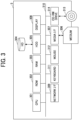
- FIG. 3 is a diagram illustrating a hardware configuration of the system control section 3.
- FIG. 2 as a function block diagram of the electrode manufacturing apparatus 1 includes a function block diagram of the system control section 3. Using FIGS. 2 and 3 , operations of the system control section 3 are described below.
- the system control section 3 includes the operation unit 34, the storage unit 35, the storage and reading unit 39, the processing unit 36, the surface detection image acquisition unit 51, the defect determination unit 52, the discharge instruction preparation unit 53, the result output unit 54, the conveyance control unit 33, and the discharge control unit 40.
- the operation unit 34 is chiefly realized by a command from the CPU 301 illustrated in FIG. 3 , and receives a signal from the keyboard 311 or the mouse 312 operated by the user, so as to accept various operations by the user.
- the operations thus accepted are each realized by a command from the CPU 301 illustrated in FIG. 3 , so as to cause various images or screens to be displayed on the display 308 provided on the operation unit 34.
- the processing unit 36 is realized by a command from the CPU 301 illustrated in FIG. 3 , and performs total control of the electrode manufacturing apparatus 1.
- the defect determination unit 52 distinguishes defects.
- the defect refers to a fault causing fall of a material characteristic value of the functional layer 12, such as a streak, a pinhole, unevenness, foreign matter, and a shortage of film thickness.
- An item in the quality information that should be regarded as a defect and such parameters as the size of a defect are assumed to be set by the user in advance. In a statement about FIGS. 6A through 6C to be given later, a streak-like defect is taken up.
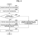
- FIG. 4 is a flowchart illustrating an example of processing for controlling the discharge amount.
- the surface detection image acquisition unit 51 acquires a surface detection image from the surface detector 8 (step S001).
- the defect determination unit 52 determines whether a streak-like defect is present (step S003), and, if the defect is not present, the log notifying that the change in discharge amount is unnecessary is prepared (step S004).
- the defect determination unit 52 instructs to prepare a discharge instruction (step S005), and the discharge instruction preparation unit 53 prepares an instruction to increase the discharge amount (step S006).
- a result with contents of the decided instruction is output from the result output unit 54 to the discharge control unit 40 (step S007).
- FIGS. 5A and 5B are conceptual diagrams of formation of the insulating layer 21 by the discharge of the liquid composition 24.
- FIGS. 5A and 5B a process for forming the insulating layer 21 in the electrode manufacturing apparatus 1 according to the present embodiment is described.
- FIG. 5A is a side view of the electrode manufacturing apparatus 1 as viewed in the Y direction
- FIG. 5B is a plan view of the electrode manufacturing apparatus 1 as viewed in a Z direction.
- FIGS. 5A and 5B the winding off part 10, the winding up part 11, the curing device 6, and the heater 7 illustrated in FIG. 1 is omitted for simplicity.
- the electrode manufacturing apparatus 1 uses the liquid composition 24 for forming the resin layer 22 or the inorganic layer 23 as the insulating layer 21 to form the resin layer 22 or the inorganic layer 23 as the insulating layer 21 so that the surface of the electrode base 9 or the surface of the functional layer 12 provided on the electrode base 9 may be covered, and detects the surface condition of the resin layer 22 or the inorganic layer 23 as the insulating layer 21 with the surface detector 8 provided downstream of the discharger 5.
- the electrode base 9 or the functional layer 12 provided on the electrode base 9 does not merely have a running pattern spread over the entire surface but may be formed by intermittent coating or in a free shape.
- a printing shape of the resin layer 22 or the inorganic layer 23 as the insulating layer 21, which is to be formed is not limited to a running pattern spread over the entire surface but may be achieved by intermittent coating or as a free shape.
- FIGS. 6A through 6C are plan views of the electrode manufacturing apparatus 1, illustrating how a streak-like defect is produced.
- FIGS. 6A through 6C description is made how a streak-like defect 59 is produced in the course of formation of the resin layer 22 or the inorganic layer 23 as the insulating layer 21.
- FIG. 6A illustrates a state where the streak-like defect 59 has been produced in the course of formation of the resin layer 22 or the inorganic layer 23 as the insulating layer 21. If the streak-like defect 59 has been produced in the course of discharge by the discharger 5, a log notifying that change in amount of discharge by the discharger 5 is unnecessary is only prepared (step S004) until the streak-like defect 59 reaches the surface detector 8.
- FIG. 6B illustrates a state where the streak-like defect 59 as produced in the course of formation of the resin layer 22 or the inorganic layer 23 as the insulating layer 21 has reached the surface detector 8. If the streak-like defect 59 reaches the surface detector 8, an instruction to increase the discharge amount is prepared by the discharge instruction preparation unit 53 (step S006). The instruction to increase the discharge amount is sent from the discharge instruction preparation unit 53 to the discharge control unit 40 through the result output unit 54 so as to increase the amount of discharge of the liquid composition 24 by the discharger 5.
- FIG. 6C illustrates a state after the instruction to increase the discharge amount is sent from the discharge instruction preparation unit 53 to the discharge control unit 40 through the result output unit 54 and the amount of discharge of the liquid composition 24 by the discharger 5 is increased.
- the discharge amount of the liquid composition 24 is increased so as to embed the streak-like defect 59 and suppress the production of another streak-like defect.
- FIGS. 7A through 7C are each another example of the diagram illustrating the general arrangement of the electrode manufacturing apparatus 1 according to the present embodiment.
- FIG. 7A illustrates the electrode manufacturing apparatus 1, which does not include the curing device 6 because the liquid composition 24 for forming the resin layer 22 or the inorganic layer 23 as the insulating layer 21 does not need a curing process.
- the surface detector 8 may be provided on an upstream side of the heater 7.
- the surface detector 8 is to detect the surface condition before drying of the liquid composition 24, the surface detector 8 is preferably provided at a stage next to the discharger 5 for the reason to be stated later.
- the surface detector 8 is preferably provided at the stage next to the discharger 5 for the reason to be stated later if the surface detector 8 is to detect the surface condition before the drying of the liquid composition 24.
- the present disclosure is chiefly effective at suppressing the production of the streak-like defect 59
- the insulating layer 21 after the production of the streak-like defect 59 illustrated in FIG. 6A is deemed to be faulty until the streak-like defect 59 is detected as illustrated in FIG. 6B and suppressed as illustrated in FIG. 6C . Therefore, the improvement in productivity attendant on the decrease in fraction defective is effected to a larger extent as the distance from the discharger 5 producing a defect to the surface detector 8 detecting a defect is shorter. Consequently, if a defect is detected before the drying of the liquid composition 24, it is desirable to provide the surface detector 8 immediately after the discharger 5, that is to say, at the stage next to the discharger 5.
- FIG. 8 illustrates an example of an optical system of the surface detector 8.
- the surface detector 8 includes, as an illumination system, a visible light source 62 that irradiates an upper face of a detection target 64 with a visible light, and an infrared/ultraviolet (IR/UV) light source 63 that emits at least one of an ultraviolet light or an infrared light.
- a visible light source 62 that irradiates an upper face of a detection target 64 with a visible light
- an infrared/ultraviolet (IR/UV) light source 63 that emits at least one of an ultraviolet light or an infrared light.
- the surface detector 8 may only include one of the light sources.
- the detection target 64 as an object of detection by the surface detector 8 refers to the electrode base 9 or the functional layer 12 provided on the electrode base 9, on which the resin layer 22 or the inorganic layer 23 as the insulating layer 21 is being formed.
- the surface detector 8 includes a visible light camera 61 as a measurement system, and the visible light camera 61 may be replaced by an IR/LTV light camera.
- the IR/UV light camera is to be arranged similarly to the visible light camera 61.
- the surface detector 8 detects a streak-like defect contained in the detection target 64, based on an output signal from the visible light camera 61 or the IR/UV light camera in such measurement system.
- FIG. 9A illustrates an example of a state where an image acquired by the surface detection image acquisition unit 51 after the detection of a defect by the surface detector 8 is displayed in the operation unit 34.
- defect type information 71 that is a result of analysis with the defect determination unit 52
- a defect spot line 73 and a defect output signal graph 74 (graph representing the change in output luminance value or luminance ratio) are collectively displayed.
- FIGS. 9B and 9C illustrate a case where the luminance value is high and a case where the luminance value is low, respectively.
- a correspondence relation between the pattern of such change (increase or decrease) in luminance value and the type of abnormality allows an accurate determination of the presence or absence of a defect and the level of a defect as a result of accumulation of experimental data for each type of abnormality that can actually occur.
- FIG. 10 is a flowchart of defect detection.
- a detection system is adjusted in a state where the detection target 64 is not arranged (step S301).
- a blue visible light source 31 is lit so as to perform image capturing with a visible light by an image capturing device 4.
- the luminance of light that directly enters the visible light camera 61 is so adjusted as to be the same or essentially the same as the upper limit of a measurable range.
- step S304 If it is determined that a defect has been detected (step S304), the processing proceeds to step S305. If it is determined that no defects have been detected (step S304), this routine is terminated.
- step S305 the type of the defect as detected is determined (step S305), and the type of the defect and defect spot information are output (step S306).
- FIG. 11 is a flowchart of discharge amount regulation based on defect spot information output.
- the surface detector 8, the surface detection image acquisition unit 51, and the defect determination unit 52 detect the defect spot information (step S401).
- the surface detection image acquisition unit 51 and the defect determination unit 52 specify the position (position in a y-axis direction) of the defect (step S402).
- the discharge instruction preparation unit 53 decides a discharge amount appropriate to the defect (an increased discharge amount, for instance) and a method for changing the discharge amount (change in discharge pattern or change in printing resolution, for instance) (step S403).
- the discharge control unit 40 controls the discharge with respect to the special position as instructed, based on the discharge amount and the discharge method as instructed (step S405).
- FIGS. 12A through 12D illustrate examples of the method for changing the discharge amount.
- the printing resolution in FIG. 12A is changed to the printing resolution in FIG. 12B .
- Such change in printing resolution is an exemplary method for increasing the discharge amount of the liquid composition 24.
- the printing resolution per unit area is changed from 3 ⁇ 3 in FIG. 12A to 4 ⁇ 4 in FIG. 12B .
- the printing resolution is changed from 3 ⁇ 3 to 4 ⁇ 4 without changing the size of dots to be printed, so as to increase the total discharge amount per unit area of the liquid composition 24.
- a printing pattern in FIG. 12C is changed to a printing pattern in FIG. 12D .
- Such change in printing pattern is another exemplary method for increasing the discharge amount of the liquid composition 24.
- the coverage rate is changed from about 56% in FIG. 12C to 100% in FIG. 12D so as to increase the total discharge amount per unit area of the liquid composition 24.
- the discharge amount may be increased over the entire region of discharge so as to embed the streak-like defect 59 or may be only increased on the periphery of a region of the streak-like defect 59.
- the surface detection image acquisition unit 51 and the defect determination unit 52 acquire information on the position in the Y direction of a defect, and the information on the position in the Y direction of a defect is additionally used by the discharge instruction preparation unit 53 to prepare a discharge instruction. In such case, the discharge amount does not need to be changed in a region other than the region of the streak-like defect 59, so that the film thickness is less affected as a whole.
- conveyance information (containing the conveyance speed and time information) on the electrode base 9 or the functional layer 12 provided on the electrode base 9, which is an object of conveyance, is considered to specify the position of a defect on the object of conveyance, as is the case with a normal production line.
- FIG. 13 is a flowchart of a method for gradually regulating the discharge amount.
- a defect is detected first and the position of the defect (the streak-like defect 59 in FIGS. 6A through 6C ) is specified.
- the position of the streak-like defect 59 on the electrode base 9 or the functional layer 12 provided on the electrode base 9 is specified from the position in the Y direction and the conveyance speed in the conveyance direction X (step S501).
- the discharge amount of the liquid composition 24, which is to be discharged to the specified position of the defect is increased in a specified amount (step S502).
- a small amount will be fine as an increment of the liquid composition 24.
- Such small amount can further prevent the liquid composition 24, to fill (make up) a defect part, from being applied to the defect part in an amount larger than the amount for properly filling the defect part.
- the defect part (the streak-like defect 59 in FIGS. 6A through 6C ) with an increased discharge amount of the liquid composition 24 is conveyed and reaches the surface detector 8, the defect part with an increased discharge amount of the liquid composition 24 is re-detected (step S503).
- the defect determination unit 52 increases again the discharge amount of the liquid composition 24, which is to be discharged to the position of the defect, in the specified amount through the discharge instruction preparation unit 53, the result output unit 54, and the discharge control unit 40 (step S502).
- the discharge pattern is changed to increase the amount of the liquid composition 24.
- the discharge pattern is changed to increase the discharge amount of the liquid composition 24, so that a defect produced at the surface of the insulating layer 21 is eliminated by a simple control.
- An electrode manufacturing apparatus (1) includes an applier (5) configured to apply a liquid composition (24) to form an insulating layer (21) onto an electrode base (9) or a functional layer (12) on the electrode base (9); a controller (40) configured to control the applier (5); and a surface detector (8) configured to detect a surface condition of the liquid composition (24) or the insulating layer (21) on the electrode base (9) or the functional layer (12), wherein the controller (40) controls the applier (5) based on the surface condition of the liquid composition (24) or the insulating layer (21) detected by the surface detector (8).
- the insulating layer (21) includes a resin layer (22).
- the insulating layer (21) includes an inorganic layer (23).
- the surface condition detected by the surface detector (8) includes a defect (59) in the liquid composition (24) or the insulating layer (21), and the controller (40) controls the applier (5) to increases an amount of the liquid composition (24) to be applied onto the defect (59) in the liquid composition (24) or the insulating layer (21).
- the surface condition includes a position of the defect (59).
- the surface condition detected by the surface detector (8) includes a defect (59) in the liquid composition (24) or the insulating layer (21), and the controller (40) controls the applier (5) to gradually increases an amount of the liquid composition (24) to be applied onto the defect (59) in the liquid composition (24) or the insulating layer (21).
- the controller (40) changes a printing resolution to increase an amount of the liquid composition (24) to be applied onto the electrode base (9) or the functional layer (12).
- the apparatus includes an applier (5) configured to apply a liquid composition (24) to form an insulating layer (21) onto an electrode base (9) or a functional layer (12) on the electrode base (9); a controller (40) configured to control the applier (5); and a surface detector (8) configured to detect a surface condition of the liquid composition (24) or the insulating layer (21) on the electrode base (9) or the functional layer (12).
- the controller (40) controls the applier (5) based on the surface condition of the liquid composition (24) or the insulating layer (21) detected by the surface detector (8).
- the method includes applying a liquid composition (24) to form an insulating layer (21) onto an electrode base (9) or a functional layer (12) on the electrode base (9); detecting a surface condition of the liquid composition (24) or the insulating layer (21) on the electrode base (9) or the functional layer (12); and controlling the applying based on the surface condition of the liquid composition (24) or the insulating layer (21) detected by the detecting.
Landscapes
- Chemical & Material Sciences (AREA)
- Engineering & Computer Science (AREA)
- Chemical Kinetics & Catalysis (AREA)
- Electrochemistry (AREA)
- General Chemical & Material Sciences (AREA)
- Manufacturing & Machinery (AREA)
- Composite Materials (AREA)
- Materials Engineering (AREA)
- Battery Electrode And Active Subsutance (AREA)
- Electric Double-Layer Capacitors Or The Like (AREA)
- Coating Apparatus (AREA)
- Fixed Capacitors And Capacitor Manufacturing Machines (AREA)
Applications Claiming Priority (1)
| Application Number | Priority Date | Filing Date | Title |
|---|---|---|---|
| JP2022039779A JP2023134867A (ja) | 2022-03-15 | 2022-03-15 | 電極製造装置、電極製造方法、電気化学素子の製造装置及び電気化学素子の製造方法 |
Publications (3)
| Publication Number | Publication Date |
|---|---|
| EP4246606A2 true EP4246606A2 (de) | 2023-09-20 |
| EP4246606A3 EP4246606A3 (de) | 2023-09-27 |
| EP4246606B1 EP4246606B1 (de) | 2025-04-02 |
Family
ID=85382496
Family Applications (1)
| Application Number | Title | Priority Date | Filing Date |
|---|---|---|---|
| EP23158381.6A Active EP4246606B1 (de) | 2022-03-15 | 2023-02-24 | Elektrodenherstellungsvorrichtung, verfahren zur herstellung einer elektrode, vorrichtung zur herstellung einer elektrochemischen vorrichtung und verfahren zur herstellung einer elektrochemischen vorrichtung |
Country Status (2)
| Country | Link |
|---|---|
| EP (1) | EP4246606B1 (de) |
| JP (1) | JP2023134867A (de) |
Citations (1)
| Publication number | Priority date | Publication date | Assignee | Title |
|---|---|---|---|---|
| JP2009266739A (ja) | 2008-04-28 | 2009-11-12 | Hitachi Vehicle Energy Ltd | 二次電池、二次電池の製造方法、及び製造システム |
Family Cites Families (8)
| Publication number | Priority date | Publication date | Assignee | Title |
|---|---|---|---|---|
| WO2011002205A2 (ko) * | 2009-06-30 | 2011-01-06 | 주식회사 엘지화학 | 다공성 코팅층을 구비한 전극의 제조방법, 이로부터 형성된 전극 및 이를 구비한 전기화학소자 |
| KR101264742B1 (ko) * | 2011-08-03 | 2013-05-14 | 삼성에스디아이 주식회사 | 전극판 형성 장치 |
| US10084168B2 (en) * | 2012-10-09 | 2018-09-25 | Johnson Battery Technologies, Inc. | Solid-state battery separators and methods of fabrication |
| EP2894698B1 (de) * | 2013-05-08 | 2017-03-01 | LG Chem, Ltd. | Elektrodenstruktur mit isolationsschicht, verfahren zur herstellung davon und elektrochemisches element damit |
| JP7279298B2 (ja) * | 2017-03-06 | 2023-05-23 | 株式会社リコー | 電極 |
| JP7547724B2 (ja) * | 2019-11-20 | 2024-09-10 | 株式会社リコー | 電極及びその製造方法並びに電気化学素子 |
| JP2021140907A (ja) * | 2020-03-04 | 2021-09-16 | 東レエンジニアリング株式会社 | Lib電極部塗布検査装置、及びlib電極部塗布検査方法 |
| US12406976B2 (en) * | 2021-07-16 | 2025-09-02 | Ricoh Company, Ltd. | Electrode manufacturing method |
-
2022
- 2022-03-15 JP JP2022039779A patent/JP2023134867A/ja active Pending
-
2023
- 2023-02-24 EP EP23158381.6A patent/EP4246606B1/de active Active
Patent Citations (1)
| Publication number | Priority date | Publication date | Assignee | Title |
|---|---|---|---|---|
| JP2009266739A (ja) | 2008-04-28 | 2009-11-12 | Hitachi Vehicle Energy Ltd | 二次電池、二次電池の製造方法、及び製造システム |
Also Published As
| Publication number | Publication date |
|---|---|
| JP2023134867A (ja) | 2023-09-28 |
| EP4246606B1 (de) | 2025-04-02 |
| EP4246606A3 (de) | 2023-09-27 |
Similar Documents
| Publication | Publication Date | Title |
|---|---|---|
| Guo et al. | New understandings of ethanol oxidation reaction mechanism on Pd/C and Pd2Ru/C catalysts in alkaline direct ethanol fuel cells | |
| JP4753870B2 (ja) | リチウムイオン二次電池の製造法 | |
| US8273482B2 (en) | Electrode | |
| CN102641822B (zh) | 用于涂覆活性材料的装置和方法 | |
| US20110143018A1 (en) | Methods and systems for making battery electrodes and devices arising therefrom | |
| JP2010236989A (ja) | 粒径分布モデル作成方法、当該粒径分布モデル作成方法を用いた燃料電池触媒の劣化予測方法、及び当該燃料電池触媒の劣化予測方法を用いた燃料電池の制御方法 | |
| US20240014397A1 (en) | Chemical-resistant elastomer binder for flexible electronics | |
| CN104916814B (zh) | 锂离子电池极片的锂粉处理系统及方法 | |
| US20100075022A1 (en) | Electrode producing method and electrode producing apparatus | |
| US9714472B2 (en) | Gas diffusion electrodes and process for production thereof | |
| HK50895A (en) | Method and device for producing a positive electrode in band form for galvanic cells | |
| EP4246606B1 (de) | Elektrodenherstellungsvorrichtung, verfahren zur herstellung einer elektrode, vorrichtung zur herstellung einer elektrochemischen vorrichtung und verfahren zur herstellung einer elektrochemischen vorrichtung | |
| JP4687695B2 (ja) | 膜電極接合体製造方法 | |
| CA3251623A1 (en) | METHOD FOR MANUFACTURING RIBBON ELECTRODES AND RELATED DEVICE | |
| JP3893731B2 (ja) | 間欠塗布装置 | |
| CN100334753C (zh) | 用于碱性蓄电池的正电极板及其制造方法 | |
| WO2015122207A1 (ja) | カーボン担持触媒 | |
| CN120253833A (zh) | 催化层在线表面缺陷快速检测方法、ccm全自动产线及生成方法 | |
| JP7225714B2 (ja) | 電極及びその製造方法、電極素子、非水電解液蓄電素子 | |
| JP2023137821A (ja) | 膜形成装置、電極素子、電気化学素子、二次電池、および膜形成方法 | |
| JP2015185317A (ja) | 触媒層形成方法および触媒層形成装置 | |
| JP2001015105A (ja) | 電池用極板の連続製造装置 | |
| US20150236352A1 (en) | Fuel cell electrodes using high density support material | |
| Godoy et al. | Identical‐Location Electron Microscopy Applications for Electrode Materials in Electrochemical Energy Systems–Fuel Cells, Electrolyzers and Batteries–A Review | |
| WO2024101085A1 (ja) | 触媒層形成用組成物及びそれを用いた触媒層の製造方法、並びにガス拡散電極及びそれを用いた電解セル |
Legal Events
| Date | Code | Title | Description |
|---|---|---|---|
| PUAI | Public reference made under article 153(3) epc to a published international application that has entered the european phase |
Free format text: ORIGINAL CODE: 0009012 |
|
| STAA | Information on the status of an ep patent application or granted ep patent |
Free format text: STATUS: REQUEST FOR EXAMINATION WAS MADE |
|
| PUAL | Search report despatched |
Free format text: ORIGINAL CODE: 0009013 |
|
| 17P | Request for examination filed |
Effective date: 20230224 |
|
| AK | Designated contracting states |
Kind code of ref document: A2 Designated state(s): AL AT BE BG CH CY CZ DE DK EE ES FI FR GB GR HR HU IE IS IT LI LT LU LV MC ME MK MT NL NO PL PT RO RS SE SI SK SM TR |
|
| AK | Designated contracting states |
Kind code of ref document: A3 Designated state(s): AL AT BE BG CH CY CZ DE DK EE ES FI FR GB GR HR HU IE IS IT LI LT LU LV MC ME MK MT NL NO PL PT RO RS SE SI SK SM TR |
|
| RIC1 | Information provided on ipc code assigned before grant |
Ipc: H01M 4/66 20060101ALI20230824BHEP Ipc: B05C 11/10 20060101ALI20230824BHEP Ipc: H01M 10/04 20060101ALI20230824BHEP Ipc: G01B 11/06 20060101ALI20230824BHEP Ipc: H01M 50/403 20210101ALI20230824BHEP Ipc: H01M 4/04 20060101AFI20230824BHEP |
|
| GRAP | Despatch of communication of intention to grant a patent |
Free format text: ORIGINAL CODE: EPIDOSNIGR1 |
|
| STAA | Information on the status of an ep patent application or granted ep patent |
Free format text: STATUS: GRANT OF PATENT IS INTENDED |
|
| INTG | Intention to grant announced |
Effective date: 20240920 |
|
| GRAS | Grant fee paid |
Free format text: ORIGINAL CODE: EPIDOSNIGR3 |
|
| P01 | Opt-out of the competence of the unified patent court (upc) registered |
Free format text: CASE NUMBER: APP_2522/2025 Effective date: 20250115 |
|
| GRAA | (expected) grant |
Free format text: ORIGINAL CODE: 0009210 |
|
| STAA | Information on the status of an ep patent application or granted ep patent |
Free format text: STATUS: THE PATENT HAS BEEN GRANTED |
|
| AK | Designated contracting states |
Kind code of ref document: B1 Designated state(s): AL AT BE BG CH CY CZ DE DK EE ES FI FR GB GR HR HU IE IS IT LI LT LU LV MC ME MK MT NL NO PL PT RO RS SE SI SK SM TR |
|
| REG | Reference to a national code |
Ref country code: GB Ref legal event code: FG4D |
|
| REG | Reference to a national code |
Ref country code: CH Ref legal event code: EP |
|
| REG | Reference to a national code |
Ref country code: IE Ref legal event code: FG4D |
|
| REG | Reference to a national code |
Ref country code: DE Ref legal event code: R096 Ref document number: 602023002650 Country of ref document: DE |
|
| REG | Reference to a national code |
Ref country code: NL Ref legal event code: MP Effective date: 20250402 |
|
| PG25 | Lapsed in a contracting state [announced via postgrant information from national office to epo] |
Ref country code: NL Free format text: LAPSE BECAUSE OF FAILURE TO SUBMIT A TRANSLATION OF THE DESCRIPTION OR TO PAY THE FEE WITHIN THE PRESCRIBED TIME-LIMIT Effective date: 20250402 |
|
| REG | Reference to a national code |
Ref country code: AT Ref legal event code: MK05 Ref document number: 1782203 Country of ref document: AT Kind code of ref document: T Effective date: 20250402 |
|
| PG25 | Lapsed in a contracting state [announced via postgrant information from national office to epo] |
Ref country code: FI Free format text: LAPSE BECAUSE OF FAILURE TO SUBMIT A TRANSLATION OF THE DESCRIPTION OR TO PAY THE FEE WITHIN THE PRESCRIBED TIME-LIMIT Effective date: 20250402 Ref country code: ES Free format text: LAPSE BECAUSE OF FAILURE TO SUBMIT A TRANSLATION OF THE DESCRIPTION OR TO PAY THE FEE WITHIN THE PRESCRIBED TIME-LIMIT Effective date: 20250402 Ref country code: PT Free format text: LAPSE BECAUSE OF FAILURE TO SUBMIT A TRANSLATION OF THE DESCRIPTION OR TO PAY THE FEE WITHIN THE PRESCRIBED TIME-LIMIT Effective date: 20250804 |
|
| REG | Reference to a national code |
Ref country code: LT Ref legal event code: MG9D |
|
| PG25 | Lapsed in a contracting state [announced via postgrant information from national office to epo] |
Ref country code: NO Free format text: LAPSE BECAUSE OF FAILURE TO SUBMIT A TRANSLATION OF THE DESCRIPTION OR TO PAY THE FEE WITHIN THE PRESCRIBED TIME-LIMIT Effective date: 20250702 Ref country code: GR Free format text: LAPSE BECAUSE OF FAILURE TO SUBMIT A TRANSLATION OF THE DESCRIPTION OR TO PAY THE FEE WITHIN THE PRESCRIBED TIME-LIMIT Effective date: 20250703 |
|
| PG25 | Lapsed in a contracting state [announced via postgrant information from national office to epo] |
Ref country code: PL Free format text: LAPSE BECAUSE OF FAILURE TO SUBMIT A TRANSLATION OF THE DESCRIPTION OR TO PAY THE FEE WITHIN THE PRESCRIBED TIME-LIMIT Effective date: 20250402 |
|
| PG25 | Lapsed in a contracting state [announced via postgrant information from national office to epo] |
Ref country code: BG Free format text: LAPSE BECAUSE OF FAILURE TO SUBMIT A TRANSLATION OF THE DESCRIPTION OR TO PAY THE FEE WITHIN THE PRESCRIBED TIME-LIMIT Effective date: 20250402 |
|
| PG25 | Lapsed in a contracting state [announced via postgrant information from national office to epo] |
Ref country code: HR Free format text: LAPSE BECAUSE OF FAILURE TO SUBMIT A TRANSLATION OF THE DESCRIPTION OR TO PAY THE FEE WITHIN THE PRESCRIBED TIME-LIMIT Effective date: 20250402 |
|
| PG25 | Lapsed in a contracting state [announced via postgrant information from national office to epo] |
Ref country code: AT Free format text: LAPSE BECAUSE OF FAILURE TO SUBMIT A TRANSLATION OF THE DESCRIPTION OR TO PAY THE FEE WITHIN THE PRESCRIBED TIME-LIMIT Effective date: 20250402 |
|
| PG25 | Lapsed in a contracting state [announced via postgrant information from national office to epo] |
Ref country code: RS Free format text: LAPSE BECAUSE OF FAILURE TO SUBMIT A TRANSLATION OF THE DESCRIPTION OR TO PAY THE FEE WITHIN THE PRESCRIBED TIME-LIMIT Effective date: 20250702 |
|
| PG25 | Lapsed in a contracting state [announced via postgrant information from national office to epo] |
Ref country code: IS Free format text: LAPSE BECAUSE OF FAILURE TO SUBMIT A TRANSLATION OF THE DESCRIPTION OR TO PAY THE FEE WITHIN THE PRESCRIBED TIME-LIMIT Effective date: 20250802 |
|
| PG25 | Lapsed in a contracting state [announced via postgrant information from national office to epo] |
Ref country code: LV Free format text: LAPSE BECAUSE OF FAILURE TO SUBMIT A TRANSLATION OF THE DESCRIPTION OR TO PAY THE FEE WITHIN THE PRESCRIBED TIME-LIMIT Effective date: 20250402 |
|
| REG | Reference to a national code |
Ref country code: DE Ref legal event code: R097 Ref document number: 602023002650 Country of ref document: DE |
|
| PG25 | Lapsed in a contracting state [announced via postgrant information from national office to epo] |
Ref country code: DK Free format text: LAPSE BECAUSE OF FAILURE TO SUBMIT A TRANSLATION OF THE DESCRIPTION OR TO PAY THE FEE WITHIN THE PRESCRIBED TIME-LIMIT Effective date: 20250402 Ref country code: SM Free format text: LAPSE BECAUSE OF FAILURE TO SUBMIT A TRANSLATION OF THE DESCRIPTION OR TO PAY THE FEE WITHIN THE PRESCRIBED TIME-LIMIT Effective date: 20250402 |
|
| PG25 | Lapsed in a contracting state [announced via postgrant information from national office to epo] |
Ref country code: CZ Free format text: LAPSE BECAUSE OF FAILURE TO SUBMIT A TRANSLATION OF THE DESCRIPTION OR TO PAY THE FEE WITHIN THE PRESCRIBED TIME-LIMIT Effective date: 20250402 |
|
| PG25 | Lapsed in a contracting state [announced via postgrant information from national office to epo] |
Ref country code: EE Free format text: LAPSE BECAUSE OF FAILURE TO SUBMIT A TRANSLATION OF THE DESCRIPTION OR TO PAY THE FEE WITHIN THE PRESCRIBED TIME-LIMIT Effective date: 20250402 |
|
| PG25 | Lapsed in a contracting state [announced via postgrant information from national office to epo] |
Ref country code: SK Free format text: LAPSE BECAUSE OF FAILURE TO SUBMIT A TRANSLATION OF THE DESCRIPTION OR TO PAY THE FEE WITHIN THE PRESCRIBED TIME-LIMIT Effective date: 20250402 |
|
| PG25 | Lapsed in a contracting state [announced via postgrant information from national office to epo] |
Ref country code: IT Free format text: LAPSE BECAUSE OF FAILURE TO SUBMIT A TRANSLATION OF THE DESCRIPTION OR TO PAY THE FEE WITHIN THE PRESCRIBED TIME-LIMIT Effective date: 20250402 |
|
| PLBE | No opposition filed within time limit |
Free format text: ORIGINAL CODE: 0009261 |
|
| STAA | Information on the status of an ep patent application or granted ep patent |
Free format text: STATUS: NO OPPOSITION FILED WITHIN TIME LIMIT |
|
| REG | Reference to a national code |
Ref country code: CH Ref legal event code: L10 Free format text: ST27 STATUS EVENT CODE: U-0-0-L10-L00 (AS PROVIDED BY THE NATIONAL OFFICE) Effective date: 20260211 |
|
| 26N | No opposition filed |
Effective date: 20260105 |
|
| PGFP | Annual fee paid to national office [announced via postgrant information from national office to epo] |
Ref country code: DE Payment date: 20260218 Year of fee payment: 4 |
|
| PGFP | Annual fee paid to national office [announced via postgrant information from national office to epo] |
Ref country code: FR Payment date: 20260219 Year of fee payment: 4 |