EP4246599A1 - Procédé de fabrication de module photovoltaïque, module de batterie, chaîne de batteries et module photovoltaïque - Google Patents
Procédé de fabrication de module photovoltaïque, module de batterie, chaîne de batteries et module photovoltaïque Download PDFInfo
- Publication number
- EP4246599A1 EP4246599A1 EP23728573.9A EP23728573A EP4246599A1 EP 4246599 A1 EP4246599 A1 EP 4246599A1 EP 23728573 A EP23728573 A EP 23728573A EP 4246599 A1 EP4246599 A1 EP 4246599A1
- Authority
- EP
- European Patent Office
- Prior art keywords
- solar cell
- polymer material
- crystalline silicon
- solder ribbon
- module
- Prior art date
- Legal status (The legal status is an assumption and is not a legal conclusion. Google has not performed a legal analysis and makes no representation as to the accuracy of the status listed.)
- Pending
Links
- 238000004519 manufacturing process Methods 0.000 title description 11
- 229910000679 solder Inorganic materials 0.000 claims abstract description 125
- 229910021419 crystalline silicon Inorganic materials 0.000 claims abstract description 110
- 239000002861 polymer material Substances 0.000 claims abstract description 107
- 238000000034 method Methods 0.000 claims abstract description 88
- 238000010438 heat treatment Methods 0.000 claims abstract description 54
- 239000000945 filler Substances 0.000 claims abstract description 37
- 238000003475 lamination Methods 0.000 claims abstract description 32
- 238000007789 sealing Methods 0.000 claims abstract description 18
- 229920002037 poly(vinyl butyral) polymer Polymers 0.000 claims description 42
- 238000005476 soldering Methods 0.000 claims description 26
- 239000004433 Thermoplastic polyurethane Substances 0.000 claims description 13
- 229920000131 polyvinylidene Polymers 0.000 claims description 13
- 229920002803 thermoplastic polyurethane Polymers 0.000 claims description 13
- 238000002844 melting Methods 0.000 claims description 11
- 230000008018 melting Effects 0.000 claims description 11
- 239000005038 ethylene vinyl acetate Substances 0.000 claims description 7
- 239000004952 Polyamide Substances 0.000 claims description 6
- 229920002647 polyamide Polymers 0.000 claims description 6
- 229920006124 polyolefin elastomer Polymers 0.000 claims description 6
- 229920006324 polyoxymethylene Polymers 0.000 claims description 6
- 229920002397 thermoplastic olefin Polymers 0.000 claims description 6
- 239000000126 substance Substances 0.000 claims description 5
- 238000001816 cooling Methods 0.000 claims description 4
- 238000007664 blowing Methods 0.000 claims description 3
- 230000009466 transformation Effects 0.000 abstract 1
- 239000010410 layer Substances 0.000 description 68
- 239000010408 film Substances 0.000 description 55
- 230000008569 process Effects 0.000 description 41
- 229920000642 polymer Polymers 0.000 description 23
- 239000011521 glass Substances 0.000 description 15
- 238000010586 diagram Methods 0.000 description 13
- 239000000463 material Substances 0.000 description 12
- 238000004806 packaging method and process Methods 0.000 description 8
- ATJFFYVFTNAWJD-UHFFFAOYSA-N Tin Chemical compound [Sn] ATJFFYVFTNAWJD-UHFFFAOYSA-N 0.000 description 7
- 230000000052 comparative effect Effects 0.000 description 7
- 239000012467 final product Substances 0.000 description 6
- 229920001200 poly(ethylene-vinyl acetate) Polymers 0.000 description 4
- 229920005989 resin Polymers 0.000 description 4
- 239000011347 resin Substances 0.000 description 4
- 230000000181 anti-adherent effect Effects 0.000 description 3
- 230000005540 biological transmission Effects 0.000 description 3
- DQXBYHZEEUGOBF-UHFFFAOYSA-N but-3-enoic acid;ethene Chemical compound C=C.OC(=O)CC=C DQXBYHZEEUGOBF-UHFFFAOYSA-N 0.000 description 3
- 238000004132 cross linking Methods 0.000 description 3
- 238000005538 encapsulation Methods 0.000 description 3
- 238000009413 insulation Methods 0.000 description 3
- 239000002356 single layer Substances 0.000 description 3
- 239000004812 Fluorinated ethylene propylene Substances 0.000 description 2
- GYHNNYVSQQEPJS-UHFFFAOYSA-N Gallium Chemical compound [Ga] GYHNNYVSQQEPJS-UHFFFAOYSA-N 0.000 description 2
- WBGNVADHURSIJJ-UHFFFAOYSA-N [In].[Pb].[Sn] Chemical compound [In].[Pb].[Sn] WBGNVADHURSIJJ-UHFFFAOYSA-N 0.000 description 2
- 239000002313 adhesive film Substances 0.000 description 2
- 239000012790 adhesive layer Substances 0.000 description 2
- 229910045601 alloy Inorganic materials 0.000 description 2
- 239000000956 alloy Substances 0.000 description 2
- 238000003491 array Methods 0.000 description 2
- 239000011248 coating agent Substances 0.000 description 2
- 238000000576 coating method Methods 0.000 description 2
- 230000009969 flowable effect Effects 0.000 description 2
- 229920002313 fluoropolymer Polymers 0.000 description 2
- 238000010030 laminating Methods 0.000 description 2
- 230000003287 optical effect Effects 0.000 description 2
- 229920009441 perflouroethylene propylene Polymers 0.000 description 2
- 229920001343 polytetrafluoroethylene Polymers 0.000 description 2
- 239000004810 polytetrafluoroethylene Substances 0.000 description 2
- 238000003825 pressing Methods 0.000 description 2
- 229910001316 Ag alloy Inorganic materials 0.000 description 1
- 229910001152 Bi alloy Inorganic materials 0.000 description 1
- RYGMFSIKBFXOCR-UHFFFAOYSA-N Copper Chemical compound [Cu] RYGMFSIKBFXOCR-UHFFFAOYSA-N 0.000 description 1
- 229910000807 Ga alloy Inorganic materials 0.000 description 1
- 229910000978 Pb alloy Inorganic materials 0.000 description 1
- -1 Polytetrafluoroethylene Polymers 0.000 description 1
- 229920001328 Polyvinylidene chloride Polymers 0.000 description 1
- 229910001245 Sb alloy Inorganic materials 0.000 description 1
- XUIMIQQOPSSXEZ-UHFFFAOYSA-N Silicon Chemical compound [Si] XUIMIQQOPSSXEZ-UHFFFAOYSA-N 0.000 description 1
- BQCADISMDOOEFD-UHFFFAOYSA-N Silver Chemical compound [Ag] BQCADISMDOOEFD-UHFFFAOYSA-N 0.000 description 1
- 229910001128 Sn alloy Inorganic materials 0.000 description 1
- 230000009471 action Effects 0.000 description 1
- 230000001070 adhesive effect Effects 0.000 description 1
- WATWJIUSRGPENY-UHFFFAOYSA-N antimony atom Chemical compound [Sb] WATWJIUSRGPENY-UHFFFAOYSA-N 0.000 description 1
- 230000009286 beneficial effect Effects 0.000 description 1
- 230000015572 biosynthetic process Effects 0.000 description 1
- JCXGWMGPZLAOME-UHFFFAOYSA-N bismuth atom Chemical compound [Bi] JCXGWMGPZLAOME-UHFFFAOYSA-N 0.000 description 1
- 238000005524 ceramic coating Methods 0.000 description 1
- 230000008859 change Effects 0.000 description 1
- 238000010924 continuous production Methods 0.000 description 1
- 229910052802 copper Inorganic materials 0.000 description 1
- 239000010949 copper Substances 0.000 description 1
- 238000005336 cracking Methods 0.000 description 1
- 230000007423 decrease Effects 0.000 description 1
- 230000007812 deficiency Effects 0.000 description 1
- 230000000694 effects Effects 0.000 description 1
- 229920001971 elastomer Polymers 0.000 description 1
- 239000000806 elastomer Substances 0.000 description 1
- 238000010292 electrical insulation Methods 0.000 description 1
- 150000002148 esters Chemical class 0.000 description 1
- HQQADJVZYDDRJT-UHFFFAOYSA-N ethene;prop-1-ene Chemical group C=C.CC=C HQQADJVZYDDRJT-UHFFFAOYSA-N 0.000 description 1
- 239000004811 fluoropolymer Substances 0.000 description 1
- 239000006260 foam Substances 0.000 description 1
- 230000004927 fusion Effects 0.000 description 1
- 229910052733 gallium Inorganic materials 0.000 description 1
- 238000007731 hot pressing Methods 0.000 description 1
- 229910052738 indium Inorganic materials 0.000 description 1
- APFVFJFRJDLVQX-UHFFFAOYSA-N indium atom Chemical compound [In] APFVFJFRJDLVQX-UHFFFAOYSA-N 0.000 description 1
- 238000009434 installation Methods 0.000 description 1
- 230000004048 modification Effects 0.000 description 1
- 238000012986 modification Methods 0.000 description 1
- 230000035699 permeability Effects 0.000 description 1
- 230000000704 physical effect Effects 0.000 description 1
- 239000004014 plasticizer Substances 0.000 description 1
- 239000005033 polyvinylidene chloride Substances 0.000 description 1
- 239000011148 porous material Substances 0.000 description 1
- 238000002360 preparation method Methods 0.000 description 1
- 230000001737 promoting effect Effects 0.000 description 1
- 238000009877 rendering Methods 0.000 description 1
- 229910052710 silicon Inorganic materials 0.000 description 1
- 239000010703 silicon Substances 0.000 description 1
- 239000004332 silver Substances 0.000 description 1
- 238000010583 slow cooling Methods 0.000 description 1
- 239000000758 substrate Substances 0.000 description 1
- 229920001169 thermoplastic Polymers 0.000 description 1
- 229920005992 thermoplastic resin Polymers 0.000 description 1
- 239000004416 thermosoftening plastic Substances 0.000 description 1
- 239000010409 thin film Substances 0.000 description 1
- 235000012431 wafers Nutrition 0.000 description 1
Images


Classifications
-
- H—ELECTRICITY
- H01—ELECTRIC ELEMENTS
- H01L—SEMICONDUCTOR DEVICES NOT COVERED BY CLASS H10
- H01L31/00—Semiconductor devices sensitive to infrared radiation, light, electromagnetic radiation of shorter wavelength or corpuscular radiation and specially adapted either for the conversion of the energy of such radiation into electrical energy or for the control of electrical energy by such radiation; Processes or apparatus specially adapted for the manufacture or treatment thereof or of parts thereof; Details thereof
- H01L31/04—Semiconductor devices sensitive to infrared radiation, light, electromagnetic radiation of shorter wavelength or corpuscular radiation and specially adapted either for the conversion of the energy of such radiation into electrical energy or for the control of electrical energy by such radiation; Processes or apparatus specially adapted for the manufacture or treatment thereof or of parts thereof; Details thereof adapted as photovoltaic [PV] conversion devices
- H01L31/042—PV modules or arrays of single PV cells
- H01L31/05—Electrical interconnection means between PV cells inside the PV module, e.g. series connection of PV cells
- H01L31/0504—Electrical interconnection means between PV cells inside the PV module, e.g. series connection of PV cells specially adapted for series or parallel connection of solar cells in a module
-
- H—ELECTRICITY
- H01—ELECTRIC ELEMENTS
- H01L—SEMICONDUCTOR DEVICES NOT COVERED BY CLASS H10
- H01L31/00—Semiconductor devices sensitive to infrared radiation, light, electromagnetic radiation of shorter wavelength or corpuscular radiation and specially adapted either for the conversion of the energy of such radiation into electrical energy or for the control of electrical energy by such radiation; Processes or apparatus specially adapted for the manufacture or treatment thereof or of parts thereof; Details thereof
- H01L31/18—Processes or apparatus specially adapted for the manufacture or treatment of these devices or of parts thereof
- H01L31/1876—Particular processes or apparatus for batch treatment of the devices
-
- H—ELECTRICITY
- H01—ELECTRIC ELEMENTS
- H01L—SEMICONDUCTOR DEVICES NOT COVERED BY CLASS H10
- H01L31/00—Semiconductor devices sensitive to infrared radiation, light, electromagnetic radiation of shorter wavelength or corpuscular radiation and specially adapted either for the conversion of the energy of such radiation into electrical energy or for the control of electrical energy by such radiation; Processes or apparatus specially adapted for the manufacture or treatment thereof or of parts thereof; Details thereof
- H01L31/18—Processes or apparatus specially adapted for the manufacture or treatment of these devices or of parts thereof
- H01L31/1804—Processes or apparatus specially adapted for the manufacture or treatment of these devices or of parts thereof comprising only elements of Group IV of the Periodic Table
-
- C—CHEMISTRY; METALLURGY
- C09—DYES; PAINTS; POLISHES; NATURAL RESINS; ADHESIVES; COMPOSITIONS NOT OTHERWISE PROVIDED FOR; APPLICATIONS OF MATERIALS NOT OTHERWISE PROVIDED FOR
- C09J—ADHESIVES; NON-MECHANICAL ASPECTS OF ADHESIVE PROCESSES IN GENERAL; ADHESIVE PROCESSES NOT PROVIDED FOR ELSEWHERE; USE OF MATERIALS AS ADHESIVES
- C09J7/00—Adhesives in the form of films or foils
-
- H—ELECTRICITY
- H01—ELECTRIC ELEMENTS
- H01L—SEMICONDUCTOR DEVICES NOT COVERED BY CLASS H10
- H01L31/00—Semiconductor devices sensitive to infrared radiation, light, electromagnetic radiation of shorter wavelength or corpuscular radiation and specially adapted either for the conversion of the energy of such radiation into electrical energy or for the control of electrical energy by such radiation; Processes or apparatus specially adapted for the manufacture or treatment thereof or of parts thereof; Details thereof
- H01L31/02—Details
- H01L31/0224—Electrodes
- H01L31/022408—Electrodes for devices characterised by at least one potential jump barrier or surface barrier
- H01L31/022425—Electrodes for devices characterised by at least one potential jump barrier or surface barrier for solar cells
-
- H—ELECTRICITY
- H01—ELECTRIC ELEMENTS
- H01L—SEMICONDUCTOR DEVICES NOT COVERED BY CLASS H10
- H01L31/00—Semiconductor devices sensitive to infrared radiation, light, electromagnetic radiation of shorter wavelength or corpuscular radiation and specially adapted either for the conversion of the energy of such radiation into electrical energy or for the control of electrical energy by such radiation; Processes or apparatus specially adapted for the manufacture or treatment thereof or of parts thereof; Details thereof
- H01L31/04—Semiconductor devices sensitive to infrared radiation, light, electromagnetic radiation of shorter wavelength or corpuscular radiation and specially adapted either for the conversion of the energy of such radiation into electrical energy or for the control of electrical energy by such radiation; Processes or apparatus specially adapted for the manufacture or treatment thereof or of parts thereof; Details thereof adapted as photovoltaic [PV] conversion devices
- H01L31/042—PV modules or arrays of single PV cells
- H01L31/048—Encapsulation of modules
- H01L31/0481—Encapsulation of modules characterised by the composition of the encapsulation material
-
- H—ELECTRICITY
- H01—ELECTRIC ELEMENTS
- H01L—SEMICONDUCTOR DEVICES NOT COVERED BY CLASS H10
- H01L31/00—Semiconductor devices sensitive to infrared radiation, light, electromagnetic radiation of shorter wavelength or corpuscular radiation and specially adapted either for the conversion of the energy of such radiation into electrical energy or for the control of electrical energy by such radiation; Processes or apparatus specially adapted for the manufacture or treatment thereof or of parts thereof; Details thereof
- H01L31/04—Semiconductor devices sensitive to infrared radiation, light, electromagnetic radiation of shorter wavelength or corpuscular radiation and specially adapted either for the conversion of the energy of such radiation into electrical energy or for the control of electrical energy by such radiation; Processes or apparatus specially adapted for the manufacture or treatment thereof or of parts thereof; Details thereof adapted as photovoltaic [PV] conversion devices
- H01L31/042—PV modules or arrays of single PV cells
- H01L31/05—Electrical interconnection means between PV cells inside the PV module, e.g. series connection of PV cells
- H01L31/0504—Electrical interconnection means between PV cells inside the PV module, e.g. series connection of PV cells specially adapted for series or parallel connection of solar cells in a module
- H01L31/0512—Electrical interconnection means between PV cells inside the PV module, e.g. series connection of PV cells specially adapted for series or parallel connection of solar cells in a module made of a particular material or composition of materials
-
- H—ELECTRICITY
- H01—ELECTRIC ELEMENTS
- H01L—SEMICONDUCTOR DEVICES NOT COVERED BY CLASS H10
- H01L31/00—Semiconductor devices sensitive to infrared radiation, light, electromagnetic radiation of shorter wavelength or corpuscular radiation and specially adapted either for the conversion of the energy of such radiation into electrical energy or for the control of electrical energy by such radiation; Processes or apparatus specially adapted for the manufacture or treatment thereof or of parts thereof; Details thereof
- H01L31/04—Semiconductor devices sensitive to infrared radiation, light, electromagnetic radiation of shorter wavelength or corpuscular radiation and specially adapted either for the conversion of the energy of such radiation into electrical energy or for the control of electrical energy by such radiation; Processes or apparatus specially adapted for the manufacture or treatment thereof or of parts thereof; Details thereof adapted as photovoltaic [PV] conversion devices
- H01L31/042—PV modules or arrays of single PV cells
- H01L31/05—Electrical interconnection means between PV cells inside the PV module, e.g. series connection of PV cells
- H01L31/0504—Electrical interconnection means between PV cells inside the PV module, e.g. series connection of PV cells specially adapted for series or parallel connection of solar cells in a module
- H01L31/0516—Electrical interconnection means between PV cells inside the PV module, e.g. series connection of PV cells specially adapted for series or parallel connection of solar cells in a module specially adapted for interconnection of back-contact solar cells
-
- Y—GENERAL TAGGING OF NEW TECHNOLOGICAL DEVELOPMENTS; GENERAL TAGGING OF CROSS-SECTIONAL TECHNOLOGIES SPANNING OVER SEVERAL SECTIONS OF THE IPC; TECHNICAL SUBJECTS COVERED BY FORMER USPC CROSS-REFERENCE ART COLLECTIONS [XRACs] AND DIGESTS
- Y02—TECHNOLOGIES OR APPLICATIONS FOR MITIGATION OR ADAPTATION AGAINST CLIMATE CHANGE
- Y02E—REDUCTION OF GREENHOUSE GAS [GHG] EMISSIONS, RELATED TO ENERGY GENERATION, TRANSMISSION OR DISTRIBUTION
- Y02E10/00—Energy generation through renewable energy sources
- Y02E10/50—Photovoltaic [PV] energy
-
- Y—GENERAL TAGGING OF NEW TECHNOLOGICAL DEVELOPMENTS; GENERAL TAGGING OF CROSS-SECTIONAL TECHNOLOGIES SPANNING OVER SEVERAL SECTIONS OF THE IPC; TECHNICAL SUBJECTS COVERED BY FORMER USPC CROSS-REFERENCE ART COLLECTIONS [XRACs] AND DIGESTS
- Y02—TECHNOLOGIES OR APPLICATIONS FOR MITIGATION OR ADAPTATION AGAINST CLIMATE CHANGE
- Y02P—CLIMATE CHANGE MITIGATION TECHNOLOGIES IN THE PRODUCTION OR PROCESSING OF GOODS
- Y02P70/00—Climate change mitigation technologies in the production process for final industrial or consumer products
- Y02P70/50—Manufacturing or production processes characterised by the final manufactured product
Definitions
- This application relates to solar cells, and more particularly to a photovoltaic (PV) module and a method for fabricating the same, and a solar cell module and a solar cell string.
- PV photovoltaic
- PV photovoltaic
- soldering refers to the process of connecting individual solar cells (e.g., crystalline silicon solar cells) in series through solder ribbons (e.g., interconnect ribbons) to increase the overall output voltage of the module.
- the solar cell strings formed by soldering are further connected in series and parallel to form solar cell arrays, which are then subject to laminated packaging to form the PV module.
- the solder ribbon is bonded to the solar cells with a film (namely, flexible connection between the solder ribbon and the solar cell).
- a film namely, flexible connection between the solder ribbon and the solar cell.
- the existing films are formed by laminating or bonding two or more layers of different polymers, where the innermost layer in direct contact with the solder ribbon and the solar cell has a higher adhesion and the outermost layer has a lower or no adhesion.
- the film formed by two or more layers of polymer materials often has high manufacturing and use costs, resulting in a higher overall manufacturing cost for the PV modules.
- An object of the present disclosure is to provide a photovoltaic (PV) module and a method for fabricating the same, a solar cell module, and a solar cell string to overcome the aforementioned deficiencies.
- PV photovoltaic
- a single layer of an isotropic polymer material is used as the bonding film to cover the side of the crystalline silicon solar cell where the solder ribbon is attached, followed by heating to allow the bonding of the solder ribbon to the crystalline silicon solar cell to obtain a solar cell module.
- Several solar cell modules are assembled into a solar cell array followed by lamination to achieve an ohmic contact between the solder ribbon and the grid line. Meanwhile, the polymer material is transformed into a filler layer, and the front and back sides of the solar cell array are packaged to obtain the PV module.
- a thin polymer layer is used herein to complete the bonding of the solder ribbon and the packaging of the PV module, which ensures the stable bonding without affecting the electrical connection performance between the solder ribbon and the crystalline silicon solar cell. Moreover, there is no need to distinguish the front and back sides of the film. Therefore, the method provided herein has simplified process, lowered material consumption, and reduced costs, and will not affect the overall light transmission of the PV module.
- this application provides method for fabricating a photovoltaic (PV) module, comprising:
- the film used in the bonding process consists of two layers of different materials, where the lower layer in contact with the solder ribbon has a larger viscosity than the upper layer. Therefore, an adhesive layer needs to be provided on the upper layer for encapsulation prior to the subsequent lamination process.
- the method provided herein requires only one layer of polymer material to complete the bonding of the solder ribbon to the crystalline silicon solar cell and the subsequent encapsulation of the sealing plate.
- the polymer material is an isotropic homogeneous film composed of a single substance, that is, the physical properties of the polymer material, such as viscosity and fluidity, do not change with the size and position within the film.
- the film used herein has the same adhesive properties on both sides.
- the thickness of the film is effectively reduced, and thus the costs are lowered.
- the film can be used without distinguishing the front and back sides, simplifying the process and reducing the error rate. It also ensures that the filler layer transformed by the single polymeric material has a high degree of homogeneity and permeability after the lamination process, which facilitates the optical gain of the module.
- the method provided herein does not require the soldering of the solder ribbon to the crystalline silicon solar cell, but rather simply placing the solder ribbon on the grid line of the surface of the crystalline silicon solar cell. Then a polymer material is used to cover the surface of the crystalline silicon solar cell, and is heated to simultaneously cover both the solder ribbon and the crystalline silicon solar cell, thus enabling an effective and firm bonding of the solder ribbon to the crystalline silicon solar cell, thereby providing a basis for the formation of the filler layer by the polymeric material in the subsequent lamination process.
- the lamination process involves heating and applying pressure.
- the soldering layer on the surface of the solder ribbon is melted and forms a metallic connection with the grid line, while the polymer material is cross-linked by heat and pressure to render an increased fluidity for filling gaps in the solar cell array.
- the solder ribbon since the solder ribbon is already pre-bonded and fixed on the solar cell, it will not move during the lamination process, but rather firmly attaching to the grid line when applying pressure.
- the melted soldering layer of the solder ribbon can form a good ohmic contact with the grid line, and the polymer material does not easy to overflow and enter the space between the solder ribbon and the crystalline silicon solar cell, thus avoiding the electrical insulation problems of the solder ribbon caused by poor contact between the solder ribbon and the crystalline silicon solar cell due to the overflow polymer material.
- the polymer material used herein is an isotropic homogeneous material with the same adhesion on both sides, it is preferred to perform multi-point mechanical gripping of the polymer material in actual production to achieve gripping and automated production of the solar cell module, the solar cell string and the solar cell arrays.
- the multi-point mechanical gripping is performed by means of a robot equipped with an anti-adhesive coating.
- the area of each contact point is less than or equal to 5% of the total area of the gripping surface of the gripping object.
- the total contact area is greater than or equal to 85% of the total area of the gripping surface of the gripping object.
- the anti-adhesive coating is any one or a combination of at least two of amorphous fluoropolymer (AF), fluorinated ethylene propylene (FEP) resin, fluoroplastic foam resin (FFR), polyfluoroalkoxy resin (PFA), Polytetrafluoroethylene (PTEE) and a ceramic coating.
- AF amorphous fluoropolymer
- FEP fluorinated ethylene propylene
- FFR fluoroplastic foam resin
- PFA polyfluoroalkoxy resin
- PTEE Polytetrafluoroethylene
- the specific sequence of the processes for making the solar cell string using the solar cell modules can be adjusted according to the actual situation.
- a plurality of individual solar cell modules can be prepared in advance and then are connected in series with a solder ribbon to obtain the solar cell string.
- the sequentially arranged crystalline silicon solar cells are directly connected in series with a solder ribbon, followed by arrangement of the polymer material on the surface of the crystalline silicon solar cells and heating at the first temperature to give the solar cell string.
- a softening point of the first polymer material and the second polymer material is no more than the first temperature; the first temperature is less than a melting point of the soldering layer of the solder ribbon, and the melting point of the soldering layer of the solder ribbon is less than or equal to the second temperature.
- the heating at the first temperature renders the polymer material a thermal adhesion, which ensures that the polymer material can be bonded to the crystalline silicon solar cell and hold the solder ribbon in place.
- the polymer material gradually cools, and returns to its original degree of cross-linking degree followed by curing to firmly lock the solder ribbon firmly in the position corresponding to the grid line.
- the melting point of the polymer material is preferably less than or equal to the second temperature allowing for a good quality of the filler layer formed by the lamination.
- the first temperature is 70-130°C excluding 130°C, such as 70°C, 75°C, 80°C, 85°C, 90°C, 95°C, 100°C, 105°C, 110°C, 115°C, 120°C, 125°C, and 129°C.
- the second temperature is 130-170°C, such as 130°C, 135°C, 140°C, 145°C, 150°C, 155°C, 160°C, 165°C, or 170°C.
- the first temperature and the second temperature are not limited to the listed values, other values not listed above are also applicable.
- the polymer material is limited for bonding at low temperatures herein.
- the heating at a first temperature in step (S 1) is preferably performed at a low temperature.
- the polymer material has a very low liquidity and does not able to enter the gap between the solder ribbon and the crystalline silicon solar cell, but can well wrap the surface of the solder ribbon and the crystalline silicon solar cell, resulting in a firm bonding of the solder ribbon.
- the first temperature is preferably 70 to 130°C excluding 130°C.
- the solder ribbon is a low-temperature solder ribbon, of which the melting point of the soldering layer is 130-170°C, so that the soldering layer of the low-temperature solder ribbon is not melted at the first temperature, but is melted at the second temperature in step (S3) to form a metallized connection with the corresponding grid wire.
- the polymer material produces a certain thermal adhesion only at the first temperature for effective bonding and fixing of the solder ribbon, and gains a good fluidity after being melted at the second temperature to fill the gaps in the solar cell array.
- the soldering layer of the above-mentioned low-temperature solder ribbon can be formed by an alloy of tin, lead, silver, bismuth, antimony and gallium, which is low-cost.
- the low-temperature solder ribbon can also be formed by a tin-lead-indium-based soldering alloy, where the tin-lead-indium-based soldering alloy comprises at least tin, lead, indium and gallium, and is costly but having a lower melting point temperature.
- One of ordinary skill in the art can select a proper low-temperature solder ribbon according to the actual situation and needs as long as the melting point of the soldering layer of the selected low-temperature soldering ribbon is 130-170°C.
- the heating at the first temperature in step (1) is performed for 1-5 s, such as, 1 s, 1.2 s, 1.4 s, 1.6 s, 1.8 s, 2 s, 2.2 s, 2.4 s, 2.6 s, 2.8 s, 3 s, 3.2 s, 3.4 s, 3.6 s, 3.8 s, 4 s, 4.2 s, 4.4 s, 4.6 s, 4.8 s and 5 s.
- the heating time is not limited to the values listed, and other values within the above range are also applicable.
- step (S1) further comprises:
- step (S1) the higher the first temperature in step (S1), the shorter the heating time should be, to prevent the degree of cross-linking and fluidity of the polymer material from changing too much.
- the polymer material After the heating is completed, the polymer material must be cooled immediately, preferably by blowing cooling to make the polymer material quickly return to its original state, so as to achieve rapid fixation of the solder ribbon, thereby avoiding the movement of the solder ribbon due to weak bonding caused by slow cooling.
- the rapid cooling also facilitates the smooth running of the gripping process of the solar cell module and ensures a stable and continuous production and assembly of the solar cell string and the solar cell array.
- a thickness of the first polymer material located on a side of the solar cell module in step (S1) is 0.02-0.6 mm, such as 0.02 mm, 0.03 mm, 0.04 mm, 0.05 mm, 0.06 mm, 0.07 mm, 0.08 mm, 0.09 mm, 0.1 mm, 0.15 mm, 0.2 mm, 0.25 mm, 0.3 mm, 0.35 mm, 0.4 mm, 0.45 mm, 0.5 mm, 0.55 mm, and 0.6 mm, but not limited to those listed values, and other values not listed above are also applicable.
- the wrapping effect to the solder ribbon is increased, and the bonding of the solder ribbon to the crystalline silicon solar cell is enhanced.
- the thicker polymer material can better fill the area other than the connection portion of the solder ribbon and the solar cell during the lamination process.
- the step (S1) further comprises: introducing a second polymer material to fill gaps in the solar cell array.
- the second polymer material is introduced into the solar cell array through a step of:
- the total thickness of the first polymer material and the second polymer material in step (S1) is 0.15-0.6 mm, preferable, 0.40-0.6 mm, such as, 0.15 mm, 0.20 mm, 0.25 mm, 0.30 mm, 0.35 mm, 0.38 mm, 0.4 mm, 0.42 mm, 0.44 mm, 0.46 mm, 0.48 mm, 0.5 mm, 0.52 mm, 0.54 mm, 0.56 mm, 0.58 mm and 0.6mm, but are not limited to the listed values, and other values not listed in the above range are also applicable.
- 0.40-0.6 mm such as, 0.15 mm, 0.20 mm, 0.25 mm, 0.30 mm, 0.35 mm, 0.38 mm, 0.4 mm, 0.42 mm, 0.44 mm, 0.46 mm, 0.48 mm, 0.5 mm, 0.52 mm, 0.54 mm, 0.56 mm, 0.58 mm and 0.6mm, but are not limited to the listed values, and other values
- step (S1) one or each of two sides of each crystalline silicon solar cell attached with a solder ribbon is covered with a first polymer material. And at the same time, the connection portion of the solder ribbon and/or the busbar, the gaps between the adjacent solar cell modules are preferably supplemented with a second polymer material to allow for a more homogeneous and complete filler layer formed by the cross-linking and fusion of the polymer material during the subsequent lamination process, and the filler layer is free of excess pores and air bubbles.
- the second polymer material is preferably in the form of strip, block, and net to fill the gaps and has a thickness similar to the first polymer material, so as to form a single layer as a whole, thus saving material and reducing costs.
- the second polymer material is laid on top of the first polymer material to form a new polymer layer.
- the total thickness of the first polymer material and the second polymer material on the same side should be limited, preferably to a total thickness of 0.4-0.6 mm. In such cases, the final filler layer is uniform and complete without being too thick and causing unnecessary losses.
- the above polymer materials are all isotropic films made of a single substance.
- the first polymer material is the same as the second polymer material.
- the polymer material specified in step (S1) is selected from the group consisting of polyvinyl butyral (PVB), ethylene vinyl acetate (EVA), polyolefin elastomer (POE), polyformaldehyde (POM), polyvinylidene (PVD), thermoplastic polyolefin (TPO), thermoplastic polyurethane (TPU) and polyamide (PA); wherein PVB refers to polyvinyl butyral ester, EVA refers to ethylene vinyl acetate copolymer, POE refers to polyolefin elastomer, POM refers to polyformaldehyde resin, PVD refers to polyvinylidene chloride, TPO refers to thermoplastic polyolefin, TPU refers to thermoplastic polyurethane elastomer, and PA refers to polyamide.
- PVB polyvinyl butyral ester
- EVA refers to ethylene vinyl acetate copolymer
- POE refers to
- the polymer material used herein is a thermoplastic resin material, such as a PVB adhesive film formed by PVB and plasticizers.
- the PVB adhesive film has the characteristics of recyclable, secondary processing, and reusable. Moreover, it can maintain its original form and will not undergo body shrinkage within the temperature interval for bonding defined herein and under the action of a certain pressure. Therefore, it can prevent the solder ribbon from moving due to the film shrinking caused by during the preparation of the solar cell string and the PV module.
- step (S3) further comprises the assembly of the solar cell modules.
- the assembly comprises the installation of a frame and a junction box.
- the front sealing plate and the back sealing plate in step (2) are both made of glass and/or polymers.
- this application provides a solar cell module fabricated by using the aforementioned method.
- this application provides a solar cell string fabricated by using the aforementioned method.
- this application further provides a PV module fabricated by using the aforementioned method
- the present disclosure has the following beneficial effects.
- the front side of the solar cell module, the solar cell string, the solar cell array and the photovoltaic (PV) module described below refers to the light-receiving side (light-facing side), and the reverse side or back side refers to the side opposite to the front side.
- PV photovoltaic
- solder ribbons used in the following embodiments and the comparative embodiments are the same.
- the melting point of the soldering layer of the solder ribbon is 138-169°C, and the substrate of the solder ribbon has a copper content of more than or equal to 99.96%.
- Such solder ribbon has the following advantages: suitable for the low-temperature soldering process of the solar cells; reducing the risk of hidden cracking of the solar cells; more suitable for thin and large-size silicon wafers; and reducing the loss of the PV module.
- a method for preparing a PV module which is applied to a solar cell with a positive electrode located on a front side of a crystalline silicon solar cell and a negative electrode located on a back side of the crystalline silicon solar cell.
- the method includes the following steps.
- a solder ribbon is successively laid on two primary grid lines on a back side of a crystalline silicon solar cell and two primary grid lines on a front side of an adjacent crystalline silicon solar cell to enable the series connection between two adjacent crystalline silicon solar cells, and in this way, 15 crystalline silicon solar cells are sequentially connected in series. Then the front and back sides of each crystalline silicon solar cell are each covered with an isotropic homogeneous polyvinylbutyral (PVB) film having a thickness of 0.5 mm.
- PVB polyvinylbutyral
- a heating device is allowed to be in direct contact with the PVB film and heat the PVB film at 70°C for 3 s, so as to obtain a solar cell string formed by 15 solar cell modules connected in series.
- Four solar cell strings are prepared and connected in parallel via busbars to form a solar cell array.
- Step (2) Stacking process
- a front glass sheet is laid on a front side of the solar cell array, and a back polymer sheet is laid on a back side of the solar cell array, so as to form a stacked body.
- the stacked body obtained in step (2) is subjected to lamination in a double-sided heating laminator at 160°C for 360 s.
- the tin layer of the solder ribbon is melted and forms a metallized connection with the grid line to form an ohmic contact.
- a front filler layer and a back filler layer are respectively formed on front and back sides of the stacked body, so as to complete the packaging of the front glass sheet and the back polymer sheet to obtain the PV module.
- a frame is arranged around the perimeter of the PV module, and a junction box is arranged on the back polymer sheet, so as to arrive at the final product.
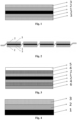
- Fig. 1 is a schematic diagram of the solar cell module obtained in step (1) of this embodiment.
- Fig. 2 is a schematic diagram of the solar cell string obtained in step (1) of this embodiment.
- the solder ribbon 2 is placed on the front and back sides of the crystalline silicon solar cell 1 in the solar cell module.
- the outer surface of the crystalline silicon solar cell 1 is covered with a polymer material 3 to enable the solder ribbon 2 to be firmly bonded to the crystalline silicon solar cell 1.
- the solar cell string includes 15 solar cell modules sequentially arranged in a straight line (only four solar cell modules are shown in Fig. 2 ).
- the solder ribbon 2 on the back side of the former solar cell module is connected to the solder ribbon 2 on the front side of the latter solar cell module, so as to enable the series connection of individual solar cell modules.
- Fig. 3 is a schematic diagram of a structure of a solar cell module of the PV module obtained in step (3) of this embodiment.
- the solar cell module includes a crystalline silicon solar cell 1.
- the front and back sides of the crystalline silicon solar cell 1 are each provided with the solder ribbon 2.
- the front and back side outer surfaces of the crystalline silicon solar cell 1 are each provided with the filler layer 4 formed by the polymer material 3.
- the exposed solder ribbon 2 and the crystalline silicon solar cell 1 are covered with the filler layer 4.
- the filler layer 4 on the front side of the crystalline silicon solar cell 1 is covered with a front sealing plate 5 made of glass, and the filler layer 4 on the back side of the crystalline silicon solar cell 1 is covered with a back sealing plate 6 made of a polymer material.
- the method includes the following steps.
- a solder ribbon is successively laid on a negative electrode grid line on a back side of a crystalline silicon solar cell and a positive electrode grid line on a back side of an adjacent crystalline silicon solar cell to enable the series connection between two adjacent crystalline silicon solar cells, and in this way, 10 crystalline silicon solar cells are sequentially connected in series in.
- the back side of each crystalline silicon solar cell is covered with an isotropic homogeneous PVB film having a thickness of 0.38 mm.
- a heating device is allowed to be in direct contact with the PVB film and heat the PVB film at 128°C for 1s, so as to obtain a solar cell string formed by 10 solar cell modules connected in series.
- Four solar cell strings are prepared and connected in parallel via busbars to form a solar cell array. Front and back sides of the solar cell array are each covered with an isotropic homogeneous PVB film having a thickness of 0.2 mm.
- Step (2) Stacking process
- a front glass sheet is laid on a front side of the solar cell array, and a back polymer sheet is laid on a back side of the solar cell array, so as to form a stacked body.
- the stacked body obtained in step (2) is subjected to lamination in a single-sided heating laminator at 140°C for 900 s.
- the tin layer of the solder ribbon is melted and metallized with the grid line to form an ohmic contact.
- a front filler layer and a back filler layer are respectively formed on front and back sides of the stacked body, so as to complete the packaging of the front glass sheet and the back polymer sheet to obtain the PV module.
- a frame is arranged around the perimeter of the PV module, and a junction box is arranged on the back polymer sheet, so as to arrive at the final product.
- the single-sided heating laminator used in step (3) of this embodiment is different from the double-sided heating laminator used in step (3) of Embodiment 1 on the speed of thermal conduction and the heating time.
- Figs. 4 and 5 are schematic diagrams of a structure of the solar cell module obtained in step (1) of this embodiment.
- Fig. 6 is a schematic diagram of a structure of the solar cell string obtained in step (1) of this embodiment.
- the solder ribbon 2 is placed on the back side of the crystalline silicon solar cell 1 in the solar cell module.
- the outer surface of the crystalline silicon solar cell 1 is covered with a polymer material 3 to enable the solder ribbon 2 to be firmly bonded to the crystalline silicon solar cell 1.
- the solar cell string includes 10 solar cell modules sequentially arranged in a straight line and spaced apart (only four solar cell modules are shown in Fig. 6 ).
- the positive electrode grid line of the former solar cell module is connected to the negative electrode grid line of the latter solar cell module through the solder ribbon 2, so as to enable the series connection of individual solar cell modules.
- Fig. 7 is a schematic diagram of a structure of a solar cell module of the PV module obtained in step (3) of this embodiment.
- the solar cell module includes a crystalline silicon solar cell 1.
- the back side of the crystalline silicon solar cell 1 is provided with the solder ribbon 2.
- the front and back side outer surfaces of the crystalline silicon solar cell 1 are each provided with the filler layer 4 formed by the polymer material 3.
- the filler layer 4 on the front side of the crystalline silicon solar cell 1 is covered with a front sealing plate 5 made of glass.
- the exposed solder ribbon 2 and the crystalline silicon solar cell 1 are covered with the filler layer 4, and the filler layer 4 on the back side of the crystalline silicon solar cell 1 is covered with a back sealing plate 6 made of a polymer material.
- the method includes the following steps.
- a solder ribbon is successively laid on a negative electrode grid line and a positive electrode grid line on a back side of a crystalline silicon solar cell.
- the back side of the crystalline silicon solar cell is covered with an isotropic homogeneous polyvinylidene (PVD) film having a thickness of 0.38 mm.
- PVD polyvinylidene
- the PVD film is heated with an infrared lamp in a non-contact long-distance manner at a heating power of 150 W and a heating temperature of about 120°C, where the infrared lamp is 20 mm away from the PVD film.
- the PVD film and the crystalline silicon solar cell are subjected to hot pressing for 1.5 s to obtain a solar cell module.
- 12 solar cell modules are sequentially prepared and arranged in a straight line.
- the positive electrode grid line of the former solar cell module is connected to the negative electrode grid line of the latter solar cell module through a solder ribbon.
- the 12 solar cell modules are connected in series to form a solar cell string.
- Six solar cell strings are prepared and connected in parallel via busbars to form a solar cell array.
- the back side of the solar cell array is covered with an isotropic homogeneous PVB film having a thickness of 0.02 mm to cover the exposed solder ribbon and busbars and fill the gaps between the solar cell modules, as shown in Fig. 8 .
- the front and back sides of the solar cell array are each covered with an isotropic homogeneous PVB film having a thickness of 0.4 mm.
- the homogeneous PVB film may be have a thickness of 0.13 mm, 0.15 mm, 0.20 mm, or 0.30 mm.
- Step (2) Stacking process
- a front glass sheet is laid on the front side of the solar cell array, and a back polymer sheet is laid on the back side of the solar cell array, so as to form a stacked body.
- the stacked body obtained in step (2) is subjected to lamination in a single-sided heating laminator at 140°C for 600 s.
- the tin layer of the solder ribbon is melted and metallized with the busbar to form an ohmic contact.
- a front filler layer and a back filler layer are respectively formed on front and back sides of the stacked body, so as to complete the packaging of the front glass sheet and the back polymer sheet to obtain the PV module.
- a frame is arranged around the perimeter of the PV module, and a junction box is arranged on the back polymer sheet, so as to arrive at the final product.
- the heating power is preferably 150-170 W.
- the heating time decreases with the increasing of the heating power, but it should be greater than or equal to 1s.
- the heating time is lower than 1s, the PVD film is not easy to adhere to the crystalline silicon solar cell.
- the heating power exceeds 170W, the PVD film will quickly shrink and not easy to bond the solder ribbon to the crystalline silicon solar cell.
- a method for preparing a PV module which is applied to a solar cell with a positive electrode located on a front side of a crystalline silicon solar cell and a negative electrode located on a back side of the crystalline silicon solar cell.
- the method includes the following steps.
- a solder ribbon is successively laid on two primary grid lines on front and back sides of a crystalline silicon solar cell. Then the front side and the back side of the crystalline silicon solar cell are each covered with an isotropic homogeneous thermoplastic polyurethane (TPU) film having a thickness of 0.1 mm.
- TPU thermoplastic polyurethane
- a heating device directly contacts with the TPU film for heating to bond the solder ribbon to the solar cell at 105°C for 3s, so as to obtain a solar cell module.
- 14 solar cell modules are prepared and sequentially arranged in a straight line. The primary grid line on the front side of the former solar cell module is connected to the primary grid line on the back side of the latter solar cell module through a solder ribbon.
- the 14 solar cell modules are connected in series to form a solar cell string.
- Five solar cell strings are prepared and connected in parallel through busbars to form a solar cell array.
- the front and back sides of the solar cell array are each covered with an isotropic homogeneous PVB net having a thickness of 0.5 mm to cover the exposed solder ribbon and busbars and fill the gaps between the solar cell modules, as shown in Fig. 9 .
- Step (2) Stacking process
- a front glass sheet is laid on the front side of the solar cell array, and a back polymer sheet is laid on the back side of the solar cell array, so as to form a stacked body.
- the stacked body obtained in step (2) is subjected to lamination in a double-sided heating laminator at 160°C for 600 s.
- the tin layer of the solder ribbon is melted and metallized with the grid line to form an ohmic contact.
- a front filler layer and a back filler layer are respectively formed on front and back sides of the stacked body, so as to complete the packaging of the front glass sheet and the back polymer sheet to obtain the PV module.
- a frame is arranged around the perimeter of the PV module, and a junction box is arranged on the back polymer sheet, so as to give the final product.
- the TPU film may be heated with an infrared lamp in a non-contact long-distance manner.
- the distance between the infrared lamp and the TPU film is about 20 mm.
- the heating power of the infrared lamp is preferably 130-140 W.
- the heating time can be reduced when the heating power is larger.
- the heating time is preferably 1 s. At this time, no bubbles between the TPU file and the crystalline silicon solar cell.
- a method for preparing a PV module which is applied to a solar cell with a positive electrode located on a front side of a crystalline silicon solar cell and a negative electrode located on a back side of the crystalline silicon solar cell.
- the method provided in this embodiment is different from the method of Embodiment 1 merely in the thickness of the PVB film used in step (1).
- the thickness of the PVB film is 0.2 mm.
- a method for preparing a PV module which is applied to a solar cell with a positive electrode located on a front side of a crystalline silicon solar cell and a negative electrode located on a back side of the crystalline silicon solar cell.
- the method provided in this embodiment is different from the method of Embodiment 1 merely in the thickness of the PVB film used in step (1).
- the thickness of the PVB film is 0.8 mm.
- a method for preparing a PV module which is applied to a solar cell with a positive electrode located on a front side of a crystalline silicon solar cell and a negative electrode located on a back side of the crystalline silicon solar cell.
- the method provided in this embodiment is different from the method of Embodiment 1 merely in the bonding temperature of the PVB film in step (1).
- the bonding temperature is 55°C.
- a method for preparing a PV module which is applied to a solar cell with a positive electrode located on a front side of a crystalline silicon solar cell and a negative electrode located on a back side of the crystalline silicon solar cell.
- the method provided in this embodiment is different from the method of Embodiment 1 merely in the bonding temperature of the PVB film in step (1).
- the bonding temperature is 145°C.
- a method for preparing a PV module which is applied to a solar cell with a positive electrode located on a front side of a crystalline silicon solar cell and a negative electrode located on a back side of the crystalline silicon solar cell.
- the method includes the following steps.
- a solder ribbon is successively laid on two primary grid lines on front and back sides of a crystalline silicon solar cell. Then the front side and the back side of the crystalline silicon solar cell are each covered with an isotropic homogeneous thermoplastic PVB film having a thickness of 0.25 mm.
- a heating device directly contacts with the PVB film for heating to bond the solder ribbon to the solar cell at 70°C for 3 s, so as to obtain a solar cell module.
- 15 solar cell modules are prepared and sequentially arranged in a straight line. The primary grid line on the front side of the former solar cell module is connected to the primary grid line on the back side of the latter solar cell module through a solder ribbon, and adjacent two solar cell modules are spaced apart.
- the 15 solar cell modules are sequentially connected in series to form a solar cell string.
- Four solar cell strings are prepared and connected in parallel through busbars to form a solar cell array.
- the front and back sides of the solar cell array are each covered with an isotropic homogeneous TPU film having a thickness of 0.25 mm.
- Step (2) Stacking process
- a front glass sheet is laid on the front side of the solar cell array, and a back polymer sheet is laid on the back side of the solar cell array, so as to form a stacked body.
- the stacked body obtained in step (2) is subjected to lamination in a double-sided heating laminator at 160°C for 360 s.
- the tin layer of the solder ribbon is melted and metallized with the grid line to form an ohmic contact.
- a front filler layer and a back filler layer are respectively formed on front and back sides of the stacked body, so as to complete the packaging of the front glass sheet and the back polymer sheet to obtain the PV module, where the front filler layer and the back filler layer both have a thickness of about 0.35 mm.
- a frame is arranged around the perimeter of the PV module, and a junction box is arranged on the back polymer sheet, so as to give the final product.
- a method for preparing a PV module which is applied to a solar cell with a positive electrode located on a front side of a crystalline silicon solar cell and a negative electrode located on a back side of the crystalline silicon solar cell.
- the method includes the following steps.
- a solder ribbon is successively laid on two primary grid lines on front and back sides of a crystalline silicon solar cell. Then the front side and the back side of the crystalline silicon solar cell are each covered with a film consisting of an ethylene vinyl acetate (EVA) layer and a PVB layer, where the film has a thickness of 0.5 mm, the EVA layer directly contacts with the solder ribbon and the crystalline silicon solar cell, the EVA layer has a thickness of 0.25 mm, and the PVB layer has a thickness of 0.25 mm.
- EVA ethylene vinyl acetate
- PVB layer has a thickness of 0.25 mm.
- a heating device directly contacts with the film for heating to bond the solder ribbon to the solar cell at 70°C for 3 s, so as to obtain a solar cell module. 15 solar cell modules are prepared and sequentially arranged in a straight line.
- the primary grid line on the front side of the former solar cell module is connected to the primary grid line on the back side of the latter solar cell module through a solder ribbon, and adjacent two solar cell modules are spaced apart. In this way, the 15 solar cell modules are sequentially connected in series to form a solar cell string.
- Four solar cell strings are prepared and connected in parallel through busbars to form a solar cell array.
- Step (2) Stacking process
- a front glass sheet is laid on the front side of the solar cell array, and a back polymer sheet is laid on the back side of the solar cell array, so as to form a stacked body.
- the stacked body obtained in step (2) is subjected to lamination in a double-sided heating laminator at 160°C for 360 s.
- the tin layer of the solder ribbon is melted and metallized with the grid line to form an ohmic contact.
- a front filler layer and a back filler layer are respectively formed on front and back sides of the stacked body, so as to complete the packaging of the front glass sheet and the back polymer sheet to obtain the PV module, where the front filler layer and the back filler layer both have a thickness of about 0.35 mm.
- a frame is arranged around the perimeter of the PV module, and a junction box is arranged on the back polymer sheet, so as to give the final product.
- Embodiments 1-4 the bonding between the solder ribbon and the crystalline silicon solar cell is good, without detachment and insulation problems the solder ribbon. No obvious bubbles and voids are observed in the filling layer.
- the front sealing plate and the back sealing plate are firmly encapsulated, and the obtained PV modules have excellent factory qualities.
- the thickness of the PVB film is lower in Embodiment 5 and higher in Embodiment 6, and is not in the preferable rang of 0.4-0.6 mm.
- the amount of PVB in Embodiment 5 is too small to fully fill the gaps in the solar cell array, while the amount of PVB in Embodiment 6 is too large and the excess polymeric material overflows, making clean-up tedious and increasing costs.
- the heating temperatures in Embodiments 7 and 8 are not in the preferable range of 70-130°C.
- the heating temperature in Embodiment 7 is too low such that the bonding between the PVB and the crystalline silicon solar cell is unable, and the solder ribbon tends to move.
- the heating temperature in Embodiment 8 is too high, which makes the PVB more flowable. Besides, as the temperature continues to increase, the PVB will enter the space between the solder ribbon and the crystalline silicon solar cell, causing insulation.
- step (1) of Comparative Embodiment 1 a second film different from the PVB film is additionally provided, while a film composed of two different materials is used in step (1) of Comparative Embodiment 2.
- the total thickness of the polymeric material in Comparative Embodiment 1 and Comparative Embodiment 2 is the same as that in Embodiment 1, two different materials are hard to fuse with each other during the lamination process, thus affecting the light transmission of the PV module.
- the method for fabricating the PV module described herein achieves the bonding of the solder ribbon and the encapsulation of the PV module by merely using a thin film. It ensures good bonding and stability without affecting the electrical connection performance between the solder ribbon and the crystalline silicon solar cell. Moreover, it is not required to distinguish the front and back sides of the bonding film when used, which simplifies the process, and reduces the material consumption and costs, and will not affect the overall light transmission of the PV module.
Landscapes
- Engineering & Computer Science (AREA)
- Computer Hardware Design (AREA)
- Microelectronics & Electronic Packaging (AREA)
- Power Engineering (AREA)
- Physics & Mathematics (AREA)
- Condensed Matter Physics & Semiconductors (AREA)
- Electromagnetism (AREA)
- General Physics & Mathematics (AREA)
- Life Sciences & Earth Sciences (AREA)
- Sustainable Development (AREA)
- Manufacturing & Machinery (AREA)
- Chemical & Material Sciences (AREA)
- Organic Chemistry (AREA)
- Sustainable Energy (AREA)
- Photovoltaic Devices (AREA)
- Materials Engineering (AREA)
Applications Claiming Priority (2)
| Application Number | Priority Date | Filing Date | Title |
|---|---|---|---|
| CN202211044155.6A CN115117206B (zh) | 2022-08-30 | 2022-08-30 | 一种光伏组件的制造方法及电池模块、电池串与光伏组件 |
| PCT/CN2023/088158 WO2023138709A1 (fr) | 2022-08-30 | 2023-04-13 | Procédé de fabrication de module photovoltaïque, module de batterie, chaîne de batteries et module photovoltaïque |
Publications (2)
| Publication Number | Publication Date |
|---|---|
| EP4246599A1 true EP4246599A1 (fr) | 2023-09-20 |
| EP4246599A4 EP4246599A4 (fr) | 2024-03-20 |
Family
ID=83335960
Family Applications (1)
| Application Number | Title | Priority Date | Filing Date |
|---|---|---|---|
| EP23728573.9A Pending EP4246599A4 (fr) | 2022-08-30 | 2023-04-13 | Procédé de fabrication de module photovoltaïque, module de batterie, chaîne de batteries et module photovoltaïque |
Country Status (5)
| Country | Link |
|---|---|
| US (1) | US11876146B2 (fr) |
| EP (1) | EP4246599A4 (fr) |
| KR (1) | KR102624958B1 (fr) |
| CN (1) | CN115117206B (fr) |
| WO (1) | WO2023138709A1 (fr) |
Families Citing this family (2)
| Publication number | Priority date | Publication date | Assignee | Title |
|---|---|---|---|---|
| CN113629168B (zh) * | 2021-07-07 | 2024-01-02 | 宁夏小牛自动化设备股份有限公司 | 一种电池片划片串焊一体化设备 |
| CN115117206B (zh) * | 2022-08-30 | 2022-12-16 | 苏州小牛自动化设备有限公司 | 一种光伏组件的制造方法及电池模块、电池串与光伏组件 |
Family Cites Families (15)
| Publication number | Priority date | Publication date | Assignee | Title |
|---|---|---|---|---|
| US20080185033A1 (en) * | 2007-02-06 | 2008-08-07 | Kalejs Juris P | Solar electric module |
| JP5484663B2 (ja) * | 2007-09-25 | 2014-05-07 | 三洋電機株式会社 | 太陽電池モジュールの製造方法 |
| JP5415396B2 (ja) * | 2010-12-22 | 2014-02-12 | デクセリアルズ株式会社 | 太陽電池モジュールの製造方法及び太陽電池モジュール |
| KR20130008918A (ko) * | 2011-07-13 | 2013-01-23 | 고려대학교 산학협력단 | 혼합형 태양전지 모듈 |
| JP2014060278A (ja) * | 2012-09-18 | 2014-04-03 | Dexerials Corp | ストリングのリペア方法、及び結晶系太陽電池モジュールの製造方法 |
| CN108604610A (zh) * | 2016-02-03 | 2018-09-28 | 三菱电机株式会社 | 太阳能电池模块及其制造方法 |
| EP3790059A1 (fr) * | 2019-09-05 | 2021-03-10 | Imec VZW | Procédés de mise en contact et d'interconnexion électrique de cellules photovoltaïques |
| CN112225981B (zh) * | 2020-09-18 | 2022-04-12 | 苏州赛伍应用技术股份有限公司 | 一种焊带载体膜及其制备方法和应用 |
| CN112289889A (zh) * | 2020-10-20 | 2021-01-29 | 无锡奥特维科技股份有限公司 | 电池串生产方法 |
| CN116960207A (zh) * | 2021-03-05 | 2023-10-27 | 浙江晶科能源有限公司 | 电池串结构和光伏组件及其制造方法 |
| CN113659031A (zh) * | 2021-07-01 | 2021-11-16 | 合肥晶澳太阳能科技有限公司 | 一种太阳能电池串、光伏组件及其制备方法 |
| CN114068735A (zh) * | 2021-11-11 | 2022-02-18 | 任佳新 | 一种异质结光伏电池组件的制作方法 |
| CN114068734A (zh) * | 2021-11-11 | 2022-02-18 | 任佳新 | 一种光伏电池组件的制造方法 |
| CN114744080B (zh) * | 2022-06-10 | 2022-10-21 | 苏州小牛自动化设备有限公司 | 一种电池串生产方法及电池串铺设设备 |
| CN115117206B (zh) * | 2022-08-30 | 2022-12-16 | 苏州小牛自动化设备有限公司 | 一种光伏组件的制造方法及电池模块、电池串与光伏组件 |
-
2022
- 2022-08-30 CN CN202211044155.6A patent/CN115117206B/zh active Active
-
2023
- 2023-04-13 WO PCT/CN2023/088158 patent/WO2023138709A1/fr unknown
- 2023-04-13 EP EP23728573.9A patent/EP4246599A4/fr active Pending
- 2023-04-13 KR KR1020237020396A patent/KR102624958B1/ko active IP Right Grant
- 2023-06-12 US US18/333,238 patent/US11876146B2/en active Active
Also Published As
| Publication number | Publication date |
|---|---|
| KR102624958B1 (ko) | 2024-01-12 |
| US11876146B2 (en) | 2024-01-16 |
| CN115117206B (zh) | 2022-12-16 |
| EP4246599A4 (fr) | 2024-03-20 |
| CN115117206A (zh) | 2022-09-27 |
| WO2023138709A1 (fr) | 2023-07-27 |
| US20230327046A1 (en) | 2023-10-12 |
Similar Documents
| Publication | Publication Date | Title |
|---|---|---|
| EP4246599A1 (fr) | Procédé de fabrication de module photovoltaïque, module de batterie, chaîne de batteries et module photovoltaïque | |
| US8187982B2 (en) | Manufacture method for photovoltaic module | |
| EP2169725B1 (fr) | Procédé de fabrication de module de pile solaire | |
| CN102386251B (zh) | 一种用软基片制备的柔性太阳能电池光伏组件 | |
| US20120006483A1 (en) | Methods for Interconnecting Solar Cells | |
| US20120138117A1 (en) | Thermoplastic wire network support for photovoltaic cells | |
| KR20150084891A (ko) | 태양 전지 스트링에 대한 고효율 구성 | |
| US11362226B1 (en) | Solar cell string, photovoltaic module and manufacturing methods therefor | |
| CN112786727B (zh) | 无主栅异质结太阳能电池组件互联用复合膜及其制备方法 | |
| WO2022247057A1 (fr) | Chaîne de cellules solaires à contact arrière et son procédé de préparation, et ensemble et système | |
| US20130098447A1 (en) | Method for manufacturing solar battery module and solar battery module manufactured by the manufacturing method | |
| US20200279965A1 (en) | Tape For Interconnecting Single Solar Cells Into Solar Cell Modules | |
| WO2023202648A1 (fr) | Procédé de fabrication de module photovoltaïque et module photovoltaïque | |
| WO2024012160A1 (fr) | Module de cellules solaires ibc et son procédé de fabrication, et chaîne de modules de cellules solaires ibc | |
| JP5430326B2 (ja) | 太陽電池モジュール | |
| CN116247120A (zh) | 光伏电池组件的制造方法及光伏电池组件 | |
| CN117153951A (zh) | 一种背接触光伏组件的生产方法及背接触光伏组件 | |
| CN103730519B (zh) | 一种柔性薄膜太阳能电池组件及其制作方法 | |
| JP2011210747A (ja) | 太陽電池モジュール及びその製造方法 | |
| KR101033259B1 (ko) | 박막 태양전지 모듈 제조 시스템의 쿠퍼 와이어 셋팅 큐어링 장치와 쿠퍼 와이어 셋팅 큐어링 공정 방법 | |
| CN103840021B (zh) | 串联型薄膜太阳能电池 | |
| CN202332901U (zh) | 软基柔性太阳能电池光伏组件 | |
| JP4061525B2 (ja) | 太陽電池モジュールの製造方法 | |
| CN116072753B (zh) | 光伏组件及制备方法 | |
| US20230178680A1 (en) | Photovoltaic cell module and manufacturing method thereof |
Legal Events
| Date | Code | Title | Description |
|---|---|---|---|
| STAA | Information on the status of an ep patent application or granted ep patent |
Free format text: STATUS: UNKNOWN |
|
| STAA | Information on the status of an ep patent application or granted ep patent |
Free format text: STATUS: THE INTERNATIONAL PUBLICATION HAS BEEN MADE |
|
| PUAI | Public reference made under article 153(3) epc to a published international application that has entered the european phase |
Free format text: ORIGINAL CODE: 0009012 |
|
| STAA | Information on the status of an ep patent application or granted ep patent |
Free format text: STATUS: REQUEST FOR EXAMINATION WAS MADE |
|
| 17P | Request for examination filed |
Effective date: 20230614 |
|
| AK | Designated contracting states |
Kind code of ref document: A1 Designated state(s): AL AT BE BG CH CY CZ DE DK EE ES FI FR GB GR HR HU IE IS IT LI LT LU LV MC ME MK MT NL NO PL PT RO RS SE SI SK SM TR |
|
| A4 | Supplementary search report drawn up and despatched |
Effective date: 20240215 |
|
| RIC1 | Information provided on ipc code assigned before grant |
Ipc: H01L 31/048 20140101ALI20240209BHEP Ipc: C09J 7/00 20180101ALI20240209BHEP Ipc: H01L 31/05 20140101ALI20240209BHEP Ipc: H01L 31/18 20060101AFI20240209BHEP |