EP4246591B1 - Herstellungsverfahren und leistungshalbleiterbauelement - Google Patents
Herstellungsverfahren und leistungshalbleiterbauelement Download PDFInfo
- Publication number
- EP4246591B1 EP4246591B1 EP22162144.4A EP22162144A EP4246591B1 EP 4246591 B1 EP4246591 B1 EP 4246591B1 EP 22162144 A EP22162144 A EP 22162144A EP 4246591 B1 EP4246591 B1 EP 4246591B1
- Authority
- EP
- European Patent Office
- Prior art keywords
- electrical insulation
- insulation layer
- semiconductor body
- top side
- semiconductor device
- Prior art date
- Legal status (The legal status is an assumption and is not a legal conclusion. Google has not performed a legal analysis and makes no representation as to the accuracy of the status listed.)
- Active
Links
Images


Classifications
-
- H—ELECTRICITY
- H10—SEMICONDUCTOR DEVICES; ELECTRIC SOLID-STATE DEVICES NOT OTHERWISE PROVIDED FOR
- H10D—INORGANIC ELECTRIC SEMICONDUCTOR DEVICES
- H10D62/00—Semiconductor bodies, or regions thereof, of devices having potential barriers
- H10D62/80—Semiconductor bodies, or regions thereof, of devices having potential barriers characterised by the materials
- H10D62/83—Semiconductor bodies, or regions thereof, of devices having potential barriers characterised by the materials being Group IV materials, e.g. B-doped Si or undoped Ge
- H10D62/832—Semiconductor bodies, or regions thereof, of devices having potential barriers characterised by the materials being Group IV materials, e.g. B-doped Si or undoped Ge being Group IV materials comprising two or more elements, e.g. SiGe
- H10D62/8325—Silicon carbide
-
- H—ELECTRICITY
- H10—SEMICONDUCTOR DEVICES; ELECTRIC SOLID-STATE DEVICES NOT OTHERWISE PROVIDED FOR
- H10D—INORGANIC ELECTRIC SEMICONDUCTOR DEVICES
- H10D12/00—Bipolar devices controlled by the field effect, e.g. insulated-gate bipolar transistors [IGBT]
- H10D12/01—Manufacture or treatment
- H10D12/031—Manufacture or treatment of IGBTs
- H10D12/032—Manufacture or treatment of IGBTs of vertical IGBTs
- H10D12/038—Manufacture or treatment of IGBTs of vertical IGBTs having a recessed gate, e.g. trench-gate IGBTs
-
- H—ELECTRICITY
- H10—SEMICONDUCTOR DEVICES; ELECTRIC SOLID-STATE DEVICES NOT OTHERWISE PROVIDED FOR
- H10D—INORGANIC ELECTRIC SEMICONDUCTOR DEVICES
- H10D64/00—Electrodes of devices having potential barriers
- H10D64/01—Manufacture or treatment
- H10D64/013—Manufacture or treatment of electrodes having a conductor capacitively coupled to a semiconductor by an insulator
- H10D64/01366—Manufacture or treatment of electrodes having a conductor capacitively coupled to a semiconductor by an insulator the semiconductor being silicon carbide
-
- H—ELECTRICITY
- H10—SEMICONDUCTOR DEVICES; ELECTRIC SOLID-STATE DEVICES NOT OTHERWISE PROVIDED FOR
- H10D—INORGANIC ELECTRIC SEMICONDUCTOR DEVICES
- H10D64/00—Electrodes of devices having potential barriers
- H10D64/01—Manufacture or treatment
- H10D64/025—Manufacture or treatment forming recessed gates, e.g. by using local oxidation
- H10D64/027—Manufacture or treatment forming recessed gates, e.g. by using local oxidation by etching at gate locations
-
- H—ELECTRICITY
- H10—SEMICONDUCTOR DEVICES; ELECTRIC SOLID-STATE DEVICES NOT OTHERWISE PROVIDED FOR
- H10P—GENERIC PROCESSES OR APPARATUS FOR THE MANUFACTURE OR TREATMENT OF DEVICES COVERED BY CLASS H10
- H10P50/00—Etching of wafers, substrates or parts of devices
-
- H—ELECTRICITY
- H10—SEMICONDUCTOR DEVICES; ELECTRIC SOLID-STATE DEVICES NOT OTHERWISE PROVIDED FOR
- H10D—INORGANIC ELECTRIC SEMICONDUCTOR DEVICES
- H10D12/00—Bipolar devices controlled by the field effect, e.g. insulated-gate bipolar transistors [IGBT]
- H10D12/411—Insulated-gate bipolar transistors [IGBT]
- H10D12/441—Vertical IGBTs
- H10D12/461—Vertical IGBTs having non-planar surfaces, e.g. having trenches, recesses or pillars in the surfaces of the emitter, base or collector regions
- H10D12/481—Vertical IGBTs having non-planar surfaces, e.g. having trenches, recesses or pillars in the surfaces of the emitter, base or collector regions having gate structures on slanted surfaces, on vertical surfaces, or in grooves, e.g. trench gate IGBTs
-
- H—ELECTRICITY
- H10—SEMICONDUCTOR DEVICES; ELECTRIC SOLID-STATE DEVICES NOT OTHERWISE PROVIDED FOR
- H10D—INORGANIC ELECTRIC SEMICONDUCTOR DEVICES
- H10D30/00—Field-effect transistors [FET]
- H10D30/01—Manufacture or treatment
- H10D30/021—Manufacture or treatment of FETs having insulated gates [IGFET]
- H10D30/027—Manufacture or treatment of FETs having insulated gates [IGFET] of lateral single-gate IGFETs
-
- H—ELECTRICITY
- H10—SEMICONDUCTOR DEVICES; ELECTRIC SOLID-STATE DEVICES NOT OTHERWISE PROVIDED FOR
- H10D—INORGANIC ELECTRIC SEMICONDUCTOR DEVICES
- H10D30/00—Field-effect transistors [FET]
- H10D30/60—Insulated-gate field-effect transistors [IGFET]
-
- H—ELECTRICITY
- H10—SEMICONDUCTOR DEVICES; ELECTRIC SOLID-STATE DEVICES NOT OTHERWISE PROVIDED FOR
- H10P—GENERIC PROCESSES OR APPARATUS FOR THE MANUFACTURE OR TREATMENT OF DEVICES COVERED BY CLASS H10
- H10P30/00—Ion implantation into wafers, substrates or parts of devices
- H10P30/20—Ion implantation into wafers, substrates or parts of devices into semiconductor materials, e.g. for doping
- H10P30/202—Ion implantation into wafers, substrates or parts of devices into semiconductor materials, e.g. for doping characterised by the semiconductor materials
- H10P30/204—Ion implantation into wafers, substrates or parts of devices into semiconductor materials, e.g. for doping characterised by the semiconductor materials into Group IV semiconductors
-
- H—ELECTRICITY
- H10—SEMICONDUCTOR DEVICES; ELECTRIC SOLID-STATE DEVICES NOT OTHERWISE PROVIDED FOR
- H10P—GENERIC PROCESSES OR APPARATUS FOR THE MANUFACTURE OR TREATMENT OF DEVICES COVERED BY CLASS H10
- H10P30/00—Ion implantation into wafers, substrates or parts of devices
- H10P30/20—Ion implantation into wafers, substrates or parts of devices into semiconductor materials, e.g. for doping
- H10P30/208—Ion implantation into wafers, substrates or parts of devices into semiconductor materials, e.g. for doping of electrically inactive species
-
- H—ELECTRICITY
- H10—SEMICONDUCTOR DEVICES; ELECTRIC SOLID-STATE DEVICES NOT OTHERWISE PROVIDED FOR
- H10P—GENERIC PROCESSES OR APPARATUS FOR THE MANUFACTURE OR TREATMENT OF DEVICES COVERED BY CLASS H10
- H10P34/00—Irradiation with electromagnetic or particle radiation of wafers, substrates or parts of devices
- H10P34/40—Irradiation with electromagnetic or particle radiation of wafers, substrates or parts of devices with high-energy radiation
Definitions
- a manufacturing method for a power semiconductor device is provided. Further, a power semiconductor device is also provided.
- Document US 2019/0296146 A1 refers to a semiconductor device that includes a silicon carbide layer; a gate electrode; a gate insulating layer disposed between the silicon carbide layer and the gate electrode; a first region disposed in the silicon carbide layer and containing nitrogen (N); and a second region disposed between the first region and the gate insulating layer, and containing at least one element selected from the group consisting of nitrogen (N), phosphorus (P), arsenic (As), antimony (Sb), scandium (Sc), yttrium (Y), lanthanum (La), lanthanoids (Ce, Pr, Nd, Pm, Sm, Eu, Gd, Tb, Dy, Ho, Er, Tm, Yb, Lu), hydrogen (H), deuterium (D), and fluorine (F).
- N nitrogen
- P phosphorus
- As arsenic
- Sb antimony
- Sc scandium
- Y yttrium
- La lanthanum
- An electrical insulation layer is applied on the semiconductor body, wherein next to the electrical insulation layer the semiconductor body is silicon-enriched by forming carbon vacancies in the vicinity of the surface of the silicon carbide body.
- the carbon vacancies are formed by electron beam irradiation treatment and then an electrical insulation layer of silicon oxide is formed on the surface.
- Document US 2002/0034852 A1 provides semiconductor devices having at least one silicon region in a silicon carbide wafer in which is fabricated a low voltage semiconductor device such as, for example, MOSFET devices, BiCMOS devices, Bipolar devices, etc., and on the same chip, at least one silicon carbide region in which is fabricated a high voltage (i.e., >1000 V) semiconductor device using techniques well known in the art, such as, for example, LDMOSFET, UMOSFET, DMOSFET, IGBT, MESFET, and JFET devices.
- a low voltage semiconductor device such as, for example, MOSFET devices, BiCMOS devices, Bipolar devices, etc.
- a high voltage (i.e., >1000 V) semiconductor device using techniques well known in the art, such as, for example, LDMOSFET, UMOSFET, DMOSFET, IGBT, MESFET, and JFET devices.
- Such devices are derived from a method for forming a silicon region on a silicon carbide substrate which comprises the steps of: providing a monocrystalline silicon carbide substrate; amorphizing at least one region of the substrate, preferably by subjecting at least a portion of a surface of the substrate to ion implantation to convert at least a portion of the substrate surface to amorphous silicon carbide producing a region of amorphous silicon carbide on a monocrystalline silicon carbide substrate; removing at least an effective amount of carbon from said amorphized region, preferably by subjecting at least a portion of the amorphous silicon carbide region to an etchant material which selectively removes carbon to produce a region of amorphous silicon on a monocrystalline silicon carbide substrate; and subjecting the monocrystalline substrate with at least a region of amorphous silicon to high temperature thermal anneal to produce a region of monocrystalline silicon on said monocrystalline silicon carbide substrate.
- a problem to be solved is to provide a power semiconductor device having improved electric behaviour.
- low-energy electron radiation is used in order to improve flat band voltage, V FB , and reduce carbon, C, defects at a SiO 2 /SiC interface.
- the method is for producing a power semiconductor device and comprises the steps as defined in claim 1.
- the concentration of C defects, D it , at the SiO 2 /n-type 4H-SiC interface should be reduced.
- pre-oxidation low-energy electron irradiation for defect reduction at the SiO 2 /n-type 4H-SiC interface is used.
- n-type channel MOSFETs different ways of reducing D it are possible, such as the post-oxidation annealing, POA, and pre-oxidation implantation, POI.
- One idea of the present method is, inter alia, to employ low energy electron irradiation in order to create a C-poor, that is, a layer rich of voids of C, also referred to as a V C -rich layer. This will act as a sink for C, leading to an improved V FB and the reduction of D it at the SiO 2 /4H-SiC interface.
- V C low energy electron irradiation is employed, with an energy between 116 keV and 210 keV. This is the minimum energy required in order to produce the displacement of C atoms, that is, V C . In this way, virtually no other defects will be formed, either complex or Si-related, as occur after impurity implantation or higher energy electron irradiation.
- [V C ] is 6 x 10 15 cm -3 .
- [V C ] becomes 3 x 10 15 cm -3 , meaning that about 3 x 10 15 cm -3 [C I ] have been injected during oxidation.
- the as-grown n-type epilayer should be irradiated with an electron dose such that [V C ] is at least 3 x 10 15 cm -3 , for example. In this way, a C-poor layer is formed and during oxidation, little C I will cluster to form D it .
- a kinetic energy of electrons of the low-energy electron radiation is at least 116 keV and is at most 210 keV. This means, for example, that at least 90% or at least 99% or at least 99.9% of the electrons of the low-energy electron radiation have said kinetic energy.
- C atoms of the SiC lattice can specifically be addressed by the radiation to be moved away from the top side.
- a dose of the low-energy electron radiation in the first portion is at least 10 10 cm -2 or is at least 10 12 cm -2 or is at least 10 14 cm -2 .
- said dose is at most 10 17 cm -2 or is at most 10 16 cm -2 or at most 10 15 cm -2 .
- the electrical insulation layer is of SiO 2 .
- the electrical insulation layer is produced by thermal growth.
- the constituents of the electrical insulation layer are provided, which are Si and O in the case of SiO 2 .
- a temperature during producing the electrical insulation layer is at least 600 °C or at least 800 °C or at least 1000 °C. Alternatively or additionally, this temperature is at most 1500 °C or at most 1300 °C or at most 1150 °C.
- the producing the electrical insulation layer includes annealing a previously applied material of the electrical insulation layer. It is possible that all or most of the material of the electrical insulation layer has been applied on the top side of the semiconductor body prior to the annealing.
- a temperature during annealing the electrical insulation layer is at least 200 °C or at least 300 °C or at least 400 °C. Alternatively or additionally, this temperature is at most 1000 °C or at most 800 °C or at most 600 °C.
- the annealing takes at least 0.5 h or at least 1 h and/or the annealing takes at most 12 h or at most 4 h. It is possible that a temperature during the annealing is lower than during application of the material of the electrical insulation layer.
- At least one temperature ramp may be applied.
- the annealing is done in a nitrogen-containing atmosphere.
- the annealing is done in an N 2 atmosphere, which may be free or virtually free of oxygen, or even in air or in one of N 2 O, NO, O 2 or O 3 .
- the same may apply for the thermal growth of the electrical insulation layer.
- the irradiating the at least one first portion is done in a nitrogen-containing atmosphere, which may be free or virtually free of oxygen, or which may be air or also in one of N 2 O, NO, O 2 or O 3 .
- the top side of the semiconductor body is a planar surface of the semiconductor body.
- the power semiconductor device may be of planar design.
- the method further includes the step of forming one or more trenches into the semiconductor body.
- the at least one trench is formed into the semiconductor body prior to irradiating the at least one first portion.
- the at least one trench may be produced by etching.
- the resulting power semiconductor device could be of a trench design.
- the at least one first portion includes side walls and a bottom face of the at least one trench. It is possible that the at least one first region is limited to the side walls and/or to the bottom face of the at least one trench.
- the method includes that prior to irradiating the at least one first portion, a mask material is applied on the top side.
- a mask material is applied on the top side.
- regions of the top side to be irradiated can be defined, or a penetration depth of the low-energy electron radiation into the semiconductor body may be adjusted by means of the mask material or by means of a thickness of the mask material, for a specified material.
- the at least one first portion is free of the mask material while remaining portions of the top side are partially or completely covered by the mask material. If the penetration depth of the low-energy electron radiation into the semiconductor body is to be adjusted by means of the mask material in the first portion, too, it is possible that the at least one first portion is partially provided with the mask material, possible with a reduced thickness compared with the other regions of the top side. Even the whole at least one first portion may be covered with a thin layer of the mask material.
- the semiconductor body is of non-stoichiometric SiC. That is, in this area the semiconductor body has a thin layer of Si 0.5+x C 0.5-x , wherein x is at least 0.001 or at least 0.01 and x is at most 0.1 or at most 0.02. Said layer has a thickness of at least 10 nm or of at least 100 nm and of at most 0.2 ⁇ m.
- a power semiconductor device as defined in claim 12 is additionally provided.
- the power semiconductor device is produced, for example, by means of the method as indicated in connection with at least one of the above-stated embodiments. Features of the power semiconductor device are therefore also disclosed for the method and vice versa.
- the power semiconductor device comprises a semiconductor body based on SiC and an electrical insulation layer applied in at least one first portion of a top side of the semiconductor body, wherein next to the electrical insulation layer the semiconductor body is silicon-enriched and, thus, poor of carbon, for example, compared with stoichiometric SiC.
- the power semiconductor device is a metal-insulator-semiconductor field-effect transistor, MISFET, or an insulated gate-bipolar transistor, IGBT.
- the power semiconductor device is configured for an operating voltage of at least 0.6 kV or of at least 1.2 kV. Alternatively or additionally, the power semiconductor device is configured for an operating voltage of at most 10 kV or of at most 6 kV.
- the power semiconductor device is configured for an operating current of at least 10 A or of at least 0.1 kA or of at least 1 kA. Alternatively or additionally, the power semiconductor device is configured for an operating current of at most 20 kA or of at most 5 kA.
- the power semiconductor device is a device selected from the following group: a metal-oxide-semiconductor field-effect transistor (MOSFET), an insulated-gate bipolar transistor (IGBT), a gate turn-off thyristor (GTO), a gate commutated thyristor (GCT), a junction gate field-effect transistor (JFET).
- MOSFET metal-oxide-semiconductor field-effect transistor
- IGBT insulated-gate bipolar transistor
- GTO gate turn-off thyristor
- GCT gate commutated thyristor
- JFET junction gate field-effect transistor
- the power semiconductor device is, for example, configured to be used to convert direct current, for example, from a battery to alternating current, for example, for an electric motor.
- the power semiconductor device may be used, for example, in vehicles like hybrid vehicles or plug-in electric vehicles or also in railways, like commuter trains.
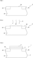
- a semiconductor body 2 is provided.
- the semiconductor body 2 is based on SiC.
- the semiconductor body 2 includes a substrate and at least one epitaxially grown semiconductor layer thereon, not shown, wherein both are based on SiC.
- the semiconductor body 2 has a plane top side 20.
- the semiconductor body 2 includes a well region 24 which may be of n-type 4H-SiC. Further there can be two p-type regions in the semiconductor body 2. These regions may be a source region 23 and a drain region 5, if the semiconductor body 2 is to be configured as a MOSFET.
- a first portion 21 of the semiconductor body 2 is irradiated with a low-energy electron radiation E.
- the first portion 21 is planar. It is possible that the low-energy electron radiation E is limited to the first portion 21 or that more of the top side 20 is exposed to the low-energy electron radiation E.
- the first portion 21 completely extends between the doped regions 23, 25 and may also include the doped regions 23, 25 partially, seen in top view of the top side 20.
- first portion 21 is illustrated in context of Figure 2 , there can be a plurality of the first portions 21. Likewise, there can be much more than two of the doped regions 24, 25.
- a kinetic energy of electrons of the low-energy electron radiation E is at least 116 keV and at most 210 keV.
- a dose of the low-energy electron radiation E in the first portion 21 is at least 10 12 cm -2 and at most 10 17 cm -2 .
- the irradiating with the radiation E is done in air or a nitrogen atmosphere.
- no vacuum may be required in the step of Figure 2 .
- an electrical insulation layer 3 is applied to the top side 20 of the semiconductor body 2 in the first portion 21.
- the electrical insulation layer 3 is produced for example, as a thermal oxide at an elevated temperature of, for example, at least 1000 °C.
- annealing can be performed, for example, in an atmosphere of one of N 2 O, NO, O 2 or O 3 .
- the electrical insulation layer 3 is of SiO 2 .
- a gate electrode 4 is formed on a side of the electrical insulation layer 3 remote from the semiconductor body 3 .
- the gate electrode 4 may be of a metal or of an ohmically conductive semiconductor material like poly-Si.
- the annealing step may be performed after applying a material of the gate electrode 4 so that combined annealing may occur.
- the finished power semiconductor device 1 is, for example, a power MOSFET or also an IGBT.
- an IGBT in case of an IGBT, of course, there is no drain region but there may be a collector region as well as a drift region.
- the finished power semiconductor device 1 is configured for currents of at least 10 A and/or of at most 10 kA.
- the power semiconductor device 1 is configured for a voltage of at least 0.6 kV and/or of at most 6 kV.
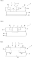
- FIGs 4 and 5 another example of a manufacturing method is illustrated.
- the semiconductor body 4 is provided, and a trench 5 is formed in the semiconductor body 2.
- the finished power semiconductor device 1 will be configured as an IGBT.
- the semiconductor body 5 includes a source region 23 at the top side 20.
- the source region 23 is divided by the trench 5 in two subregions.
- the source region 23 is embedded in the well region 24.
- electrodes for the various semiconductor regions 23, 24, 25 are not illustrate for simplifying the drawing.
- the trench 5 extends from the top side 20 into the drift region 26 and terminates within the drift region 26.
- the trench 5 does not need to have a planar bottom face but could have a rounded bottom face or even a V-shaped bottom region, seen in cross-section perpendicular with the top side 20.
- the first portion 21 could be composed of said side walls and bottom face.
- Other parts of the top side 20, outside the trench 5, may also be irradiated with the low-energy electron radiation E.
- the electrical insulation layer 3 is applied on the side walls and on the bottom face of the trench 5.
- the electrical insulation layer 5 has a constant thickness all along the trench side walls and the bottom face, however, it is also possible that the electrical insulation layer 3 has a varying thickness.
- FIG. 6 another method to produce the power semiconductor device 1 is illustrated.
- a mask material 6 is applied to the top side 20 outside the first portion 21.
- second portions 22 outside the first portion 21 may not be irradiated with the low-energy electron radiation E.
- the first portion 21 can be accurately defined by the mask material 6.
- a thickness of the mask material 6 can amount to at least 10 ⁇ m or to at least 30 ⁇ m, for example.
- Figure 7 shows a comparison of a measured voltage U vs. capacitance C characteristic between an exemplary embodiment of a power semiconductor device 1 described herein and a modified device 9.
- the modified device 9 corresponds to the power semiconductor device 1 beside the irradiating with the low-energy electron radiation E.
- Both devices 1, 9 are MOS capacitors.
- Figure 8 shows a comparison of a measured temperature T vs. constant capacitance deep level transient spectroscopy, CC-DLTS, signal S characteristic between the MOS device 1 and the reference device 9. It can be seen that the CC-DLTS signal of the pre-irradiated device 1 is lower than that of the reference device 9, implying a lower D it . This occurs in the low temperature side of the CC-DLTS spectrum, that is, close to the conduction band edge.
- ON1, ON2, OF1, OF2 may be regarded as labels only.
- Each electrically active level is located in the bandgap. For instance, OF1 is to be found at 0.19 eV below the conduction band edge. Electrically active levels give rise to a potential well, in which electrons fall. This well has a cross section. The larger, the easier to capture electrons. Also, each electrically active level is linked to a defect which, in turn, has a specified concentration.
- Figure 9 shows a comparison of a V GS vs. I GS characteristic between an exemplary embodiment of a power semiconductor device 1 described herein and a modified device 9
- Figure 10 shows a comparison of a V DS vs. I DS characteristic between an exemplary embodiment of a power semiconductor device 1 described herein and a modified device 9.
- Figure 9 refers to transfer characteristics and Figure 10 to output characteristics, with same threshold, of the reference device 9 and pre-oxidation irradiated MOSFET 1 described herein.
- simulations performed on a MOSFET, with standard or lower D it levels show an improvement of the transfer characteristics if irradiation prior to application of the electrical insulation layer is performed.
- Figure 10 show the output characteristics of the same MOSFETs. It can be seen that the curve of the irradiated MOSFET 1 shows an improvement with respect to the reference one 9, meaning that the on-resistance, R ON , has decreased.
Landscapes
- Formation Of Insulating Films (AREA)
- Insulated Gate Type Field-Effect Transistor (AREA)
- Electrodes Of Semiconductors (AREA)
Claims (13)
- Verfahren zur Herstellung einer Leistungshalbleitervorrichtung (1), umfassend die folgenden Schritte:- Bereitstellen eines Halbleiterbodys (2) auf der Basis von SiC,- Bestrahlen mindestens eines ersten Abschnitts (21) einer Oberseite (20) des Halbleiterbodys (2) mit niederenergetischer Elektronenstrahlung (E), wobei eine kinetische Energie von Elektronen der niederenergetischen Elektronenstrahlung (E) mindestens 116 keV und höchstens 210 keV beträgt, wobei mittels der niederenergetischen Elektronenstrahlung (E) in dem mindestens einen Abschnitt (21) Kohlenstoffatome (20) in den Halbleiterbody (2) bewegt werden, sodass nach dem Bestrahlen des mindestens einen Abschnitts der Halbleiterbody dort eine Schicht aus Si0,5+xC0,5-x aufweist, wobei x mindestens 0,001 und höchstens 0,1 beträgt und die Schicht eine Dicke von mindestens 10 nm und höchstens 0,2 µm aufweist, und- Herstellen einer elektrischen Isolationsschicht (3) zumindest in dem mindestens einen bestrahlten ersten Abschnitt (21),wobei die elektrische Isolationsschicht (3) aus SiOz ist.
- System nach dem vorhergehenden Anspruch,
wobei die elektrische Isolationsschicht (3) als ein Thermooxid bei einer erhöhten Temperatur von mindestens 1000 °C und höchstens 1500 °C hergestellt wird. - Verfahren nach einem der vorhergehenden Ansprüche, wobei eine Dosis der niederenergetischen Elektronenstrahlung (E) im ersten Abschnitt (21) mindestens 1012 cm-2 und höchstens 1017 cm-2 beträgt.
- Verfahren nach Anspruch 2,
wobei die elektrische Isolationsschicht (3) bei einer Temperatur von höchstens 1150 °C durch thermisches Wachstum hergestellt wird. - System nach einem der vorhergehenden Ansprüche,
wobei das Herstellen der elektrischen Isolationsschicht (3) ein Tempern eines zuvor aufgebrachten Materials der elektrischen Isolationsschicht (3) umfasst. - System nach dem vorhergehenden Anspruch,
wobei das Tempern in einer Atmosphäre erfolgt, die mindestens eines von Stickstoff und Sauerstoff enthält. - Verfahren nach einem der vorhergehenden Ansprüche, wobei das Bestrahlen des mindestens einen ersten Abschnitts (21) in einer stickstoffhaltigen Atmosphäre erfolgt.
- Verfahren nach einem der vorhergehenden Ansprüche, wobei die Oberseite (20) eine planare Oberfläche des Halbleiterbodys (2) ist.
- Verfahren nach einem der Ansprüche 1 bis 7, ferner umfassend ein Bilden mindestens eines Grabens (5) in den Hableiterbody (2) vor dem Bestrahlen des mindestens einen ersten Abschnitts (21),
wobei der mindestens eine erste Abschnitt (21) Seitenwände und eine Bodenfläche des mindestens einen Grabens (5) umfasst. - Verfahren nach einem der vorhergehenden Ansprüche, wobei vor dem Bestrahlen des mindestens einen ersten Abschnitts (21) ein Maskenmaterial (6) auf die Oberseite (20) aufgebracht wird und während des Bestrahlens des mindestens einen Abschnitts (21) der mindestens eine Abschnitt (21) frei von dem Maskenmaterial (6) ist, während restliche Abschnitte der Oberseite (20) vom Maskenmaterial (6) bedeckt werden.
- Verfahren nach einem der vorhergehenden Ansprüche, wobei auf einer Seite der elektrischen Isolationsschicht (3) entfernt vom Halbleiterbody (2) eine Gateelektrode (4) gebildet wird, wobei die Gateelektrode (4) aus Poly-Si ist.
- Leistungshalbleitervorrichtung (1), umfassend:- einen Halbleiterbody (2) auf der Basis von SiC und- eine elektrische Isolationsschicht (3), die in mindestens einem ersten Abschnitt (21) einer Oberseite (20) des Halbleiterbodys (2) aufgebracht ist,wobei neben der elektrischen Isolationsschicht (3) der Halbleiterbody (2) mit Silizium angereicht ist,wobei neben der elektrischen Isolationsschicht (3) der Halbleiterbody eine Schicht aus Si0,5+xC0,5-x aufweist und x mindestens 0,001 und höchstens 0,1 beträgt, wobei die Schicht eine Dicke von mindestens 10 nm und höchstens 0,2 µm aufweist, undwobei die elektrische Isolationsschicht (3) aus SiOz ist.
- Leistungshalbleitervorrichtung (1) nach dem vorhergehenden Anspruch,
wobei es sich um einen Metall-Isolator-Halbleiter-Feldeffekttransistor oder einen Bipolartransistor mit isolierter Gateelektrode handelt.
Priority Applications (5)
| Application Number | Priority Date | Filing Date | Title |
|---|---|---|---|
| EP22162144.4A EP4246591B1 (de) | 2022-03-15 | 2022-03-15 | Herstellungsverfahren und leistungshalbleiterbauelement |
| CN202380028158.7A CN118891735A (zh) | 2022-03-15 | 2023-01-30 | 制造方法和功率半导体器件 |
| PCT/EP2023/052132 WO2023174610A1 (en) | 2022-03-15 | 2023-01-30 | Manufacturing method and power semiconductor device |
| US18/846,211 US12453150B2 (en) | 2022-03-15 | 2023-01-30 | Manufacturing method for power semiconductor device using low-energy electron radiation to produce silicon-enriched layer |
| JP2024554981A JP7657381B1 (ja) | 2022-03-15 | 2023-01-30 | 製造方法およびパワー半導体デバイス |
Applications Claiming Priority (1)
| Application Number | Priority Date | Filing Date | Title |
|---|---|---|---|
| EP22162144.4A EP4246591B1 (de) | 2022-03-15 | 2022-03-15 | Herstellungsverfahren und leistungshalbleiterbauelement |
Publications (2)
| Publication Number | Publication Date |
|---|---|
| EP4246591A1 EP4246591A1 (de) | 2023-09-20 |
| EP4246591B1 true EP4246591B1 (de) | 2024-07-31 |
Family
ID=80786557
Family Applications (1)
| Application Number | Title | Priority Date | Filing Date |
|---|---|---|---|
| EP22162144.4A Active EP4246591B1 (de) | 2022-03-15 | 2022-03-15 | Herstellungsverfahren und leistungshalbleiterbauelement |
Country Status (5)
| Country | Link |
|---|---|
| US (1) | US12453150B2 (de) |
| EP (1) | EP4246591B1 (de) |
| JP (1) | JP7657381B1 (de) |
| CN (1) | CN118891735A (de) |
| WO (1) | WO2023174610A1 (de) |
Families Citing this family (2)
| Publication number | Priority date | Publication date | Assignee | Title |
|---|---|---|---|---|
| CN119789447B (zh) * | 2024-12-19 | 2025-08-08 | 上海华虹挚芯电子科技有限公司 | 一种沟槽型rc-igbt器件及其制造办法 |
| CN120671618B (zh) * | 2025-08-22 | 2025-10-28 | 江苏丽隽功率半导体有限公司 | SiC MOS动态特性预测方法、系统及介质 |
Family Cites Families (9)
| Publication number | Priority date | Publication date | Assignee | Title |
|---|---|---|---|---|
| US6303508B1 (en) * | 1999-12-16 | 2001-10-16 | Philips Electronics North America Corporation | Superior silicon carbide integrated circuits and method of fabricating |
| JP2011109018A (ja) * | 2009-11-20 | 2011-06-02 | Kansai Electric Power Co Inc:The | バイポーラ半導体素子 |
| JP5610492B2 (ja) | 2009-12-16 | 2014-10-22 | 国立大学法人 奈良先端科学技術大学院大学 | SiC半導体素子およびその作製方法 |
| KR20130076314A (ko) * | 2011-12-28 | 2013-07-08 | 삼성전자주식회사 | 파워소자 및 이의 제조방법 |
| JP6690198B2 (ja) * | 2015-11-16 | 2020-04-28 | 富士電機株式会社 | 炭化珪素半導体装置の製造方法 |
| JP2018186140A (ja) | 2017-04-24 | 2018-11-22 | 富士電機株式会社 | 炭化珪素半導体装置および炭化珪素半導体装置の製造方法 |
| JP6862384B2 (ja) * | 2018-03-21 | 2021-04-21 | 株式会社東芝 | 半導体装置、半導体装置の製造方法、インバータ回路、駆動装置、車両、及び、昇降機 |
| JP7100769B2 (ja) | 2018-12-07 | 2022-07-13 | ヒタチ・エナジー・スウィツァーランド・アクチェンゲゼルシャフト | 縦型炭化珪素パワーmosfetおよびigbtならびにその製造方法 |
| CN114005742B (zh) | 2021-10-09 | 2025-05-13 | 华中科技大学 | 电子辐照下SiC MOSFET阈值电压恢复方法及装置 |
-
2022
- 2022-03-15 EP EP22162144.4A patent/EP4246591B1/de active Active
-
2023
- 2023-01-30 JP JP2024554981A patent/JP7657381B1/ja active Active
- 2023-01-30 CN CN202380028158.7A patent/CN118891735A/zh active Pending
- 2023-01-30 US US18/846,211 patent/US12453150B2/en active Active
- 2023-01-30 WO PCT/EP2023/052132 patent/WO2023174610A1/en not_active Ceased
Also Published As
| Publication number | Publication date |
|---|---|
| WO2023174610A1 (en) | 2023-09-21 |
| EP4246591A1 (de) | 2023-09-20 |
| US20250113570A1 (en) | 2025-04-03 |
| JP7657381B1 (ja) | 2025-04-04 |
| US12453150B2 (en) | 2025-10-21 |
| JP2025509671A (ja) | 2025-04-11 |
| CN118891735A (zh) | 2024-11-01 |
Similar Documents
| Publication | Publication Date | Title |
|---|---|---|
| JP5295274B2 (ja) | イオン注入及び側方拡散による炭化シリコンパワーデバイスの自己整列的な製造方法 | |
| CN1132225C (zh) | 通过受控退火制造碳化硅功率器件的方法 | |
| US9142663B2 (en) | Silicon carbide devices having smooth channels | |
| US7883949B2 (en) | Methods of forming silicon carbide switching devices including P-type channels | |
| EP2740148B1 (de) | Herstellung von sic-mosfets mit hoher kanalmobilität durch behandlung der oxidschnittstelle mit cäsiumionen | |
| EP2618380A1 (de) | Halbleiterbauelement und herstellungsverfahren dafür | |
| EP0693222A1 (de) | Verfahren zur herstellung eines siliziumkarbid-feldeffekttransistors | |
| US12453150B2 (en) | Manufacturing method for power semiconductor device using low-energy electron radiation to produce silicon-enriched layer | |
| KR101386132B1 (ko) | 트렌치 구조를 갖는 SiC MOSFET 및 그 제조방법 | |
| Cheng et al. | 4H-SiC UMOSFET with an electric field modulation region below P-body | |
| Khan et al. | High-voltage UMOSFETs in 4H SiC | |
| JP3893734B2 (ja) | 炭化珪素半導体装置の製造方法 | |
| Cai et al. | The Optimization of the Specific On-Resistance of the VDMOS on the Integrated Platform of VDMOS and LDMOS | |
| US20240387620A1 (en) | Mosfets with implanted charge compensation regions | |
| US12382707B1 (en) | Conductive channel structure for SiC devices, fully integrated SiC device and fully integrated manufacturing process thereof | |
| EP4231358B1 (de) | Transistor, leistungselektronische schaltvorrichtung und verfahren zur herstellung eines transistors | |
| US20250014902A1 (en) | Method of manufacturing a semiconductor device including ion implantation processes | |
| Schustereder | Challenges for ion implantation in power device processing | |
| JP2026516365A (ja) | 注入形成された電荷補償領域を有するmosfet | |
| JP2025531221A (ja) | SiC MOSFETにおけるチャネル移動度を向上させる方法 | |
| JPS6390169A (ja) | 絶縁ゲ−ト形電界効果トランジスタ |
Legal Events
| Date | Code | Title | Description |
|---|---|---|---|
| PUAI | Public reference made under article 153(3) epc to a published international application that has entered the european phase |
Free format text: ORIGINAL CODE: 0009012 |
|
| STAA | Information on the status of an ep patent application or granted ep patent |
Free format text: STATUS: EXAMINATION IS IN PROGRESS |
|
| 17P | Request for examination filed |
Effective date: 20230601 |
|
| AK | Designated contracting states |
Kind code of ref document: A1 Designated state(s): AL AT BE BG CH CY CZ DE DK EE ES FI FR GB GR HR HU IE IS IT LI LT LU LV MC MK MT NL NO PL PT RO RS SE SI SK SM TR |
|
| RAP1 | Party data changed (applicant data changed or rights of an application transferred) |
Owner name: HITACHI ENERGY LTD |
|
| GRAP | Despatch of communication of intention to grant a patent |
Free format text: ORIGINAL CODE: EPIDOSNIGR1 |
|
| STAA | Information on the status of an ep patent application or granted ep patent |
Free format text: STATUS: GRANT OF PATENT IS INTENDED |
|
| INTG | Intention to grant announced |
Effective date: 20240304 |
|
| GRAS | Grant fee paid |
Free format text: ORIGINAL CODE: EPIDOSNIGR3 |
|
| GRAA | (expected) grant |
Free format text: ORIGINAL CODE: 0009210 |
|
| STAA | Information on the status of an ep patent application or granted ep patent |
Free format text: STATUS: THE PATENT HAS BEEN GRANTED |
|
| P01 | Opt-out of the competence of the unified patent court (upc) registered |
Effective date: 20240529 |
|
| AK | Designated contracting states |
Kind code of ref document: B1 Designated state(s): AL AT BE BG CH CY CZ DE DK EE ES FI FR GB GR HR HU IE IS IT LI LT LU LV MC MK MT NL NO PL PT RO RS SE SI SK SM TR |
|
| REG | Reference to a national code |
Ref country code: CH Ref legal event code: EP Ref country code: GB Ref legal event code: FG4D |
|
| REG | Reference to a national code |
Ref country code: DE Ref legal event code: R096 Ref document number: 602022004882 Country of ref document: DE |
|
| REG | Reference to a national code |
Ref country code: IE Ref legal event code: FG4D |
|
| REG | Reference to a national code |
Ref country code: DE Ref legal event code: R079 Ref document number: 602022004882 Country of ref document: DE Free format text: PREVIOUS MAIN CLASS: H01L0029160000 Ipc: H10D0062830000 |
|
| REG | Reference to a national code |
Ref country code: LT Ref legal event code: MG9D |
|
| REG | Reference to a national code |
Ref country code: NL Ref legal event code: MP Effective date: 20240731 |
|
| PG25 | Lapsed in a contracting state [announced via postgrant information from national office to epo] |
Ref country code: PT Free format text: LAPSE BECAUSE OF FAILURE TO SUBMIT A TRANSLATION OF THE DESCRIPTION OR TO PAY THE FEE WITHIN THE PRESCRIBED TIME-LIMIT Effective date: 20241202 |
|
| REG | Reference to a national code |
Ref country code: AT Ref legal event code: MK05 Ref document number: 1709325 Country of ref document: AT Kind code of ref document: T Effective date: 20240731 |
|
| PG25 | Lapsed in a contracting state [announced via postgrant information from national office to epo] |
Ref country code: PT Free format text: LAPSE BECAUSE OF FAILURE TO SUBMIT A TRANSLATION OF THE DESCRIPTION OR TO PAY THE FEE WITHIN THE PRESCRIBED TIME-LIMIT Effective date: 20241202 |
|
| PG25 | Lapsed in a contracting state [announced via postgrant information from national office to epo] |
Ref country code: NO Free format text: LAPSE BECAUSE OF FAILURE TO SUBMIT A TRANSLATION OF THE DESCRIPTION OR TO PAY THE FEE WITHIN THE PRESCRIBED TIME-LIMIT Effective date: 20241031 |
|
| PG25 | Lapsed in a contracting state [announced via postgrant information from national office to epo] |
Ref country code: PL Free format text: LAPSE BECAUSE OF FAILURE TO SUBMIT A TRANSLATION OF THE DESCRIPTION OR TO PAY THE FEE WITHIN THE PRESCRIBED TIME-LIMIT Effective date: 20240731 Ref country code: FI Free format text: LAPSE BECAUSE OF FAILURE TO SUBMIT A TRANSLATION OF THE DESCRIPTION OR TO PAY THE FEE WITHIN THE PRESCRIBED TIME-LIMIT Effective date: 20240731 Ref country code: GR Free format text: LAPSE BECAUSE OF FAILURE TO SUBMIT A TRANSLATION OF THE DESCRIPTION OR TO PAY THE FEE WITHIN THE PRESCRIBED TIME-LIMIT Effective date: 20241101 Ref country code: NL Free format text: LAPSE BECAUSE OF FAILURE TO SUBMIT A TRANSLATION OF THE DESCRIPTION OR TO PAY THE FEE WITHIN THE PRESCRIBED TIME-LIMIT Effective date: 20240731 |
|
| PG25 | Lapsed in a contracting state [announced via postgrant information from national office to epo] |
Ref country code: BG Free format text: LAPSE BECAUSE OF FAILURE TO SUBMIT A TRANSLATION OF THE DESCRIPTION OR TO PAY THE FEE WITHIN THE PRESCRIBED TIME-LIMIT Effective date: 20240731 |
|
| PG25 | Lapsed in a contracting state [announced via postgrant information from national office to epo] |
Ref country code: LV Free format text: LAPSE BECAUSE OF FAILURE TO SUBMIT A TRANSLATION OF THE DESCRIPTION OR TO PAY THE FEE WITHIN THE PRESCRIBED TIME-LIMIT Effective date: 20240731 |
|
| PG25 | Lapsed in a contracting state [announced via postgrant information from national office to epo] |
Ref country code: AT Free format text: LAPSE BECAUSE OF FAILURE TO SUBMIT A TRANSLATION OF THE DESCRIPTION OR TO PAY THE FEE WITHIN THE PRESCRIBED TIME-LIMIT Effective date: 20240731 Ref country code: IS Free format text: LAPSE BECAUSE OF FAILURE TO SUBMIT A TRANSLATION OF THE DESCRIPTION OR TO PAY THE FEE WITHIN THE PRESCRIBED TIME-LIMIT Effective date: 20241130 |
|
| PG25 | Lapsed in a contracting state [announced via postgrant information from national office to epo] |
Ref country code: HR Free format text: LAPSE BECAUSE OF FAILURE TO SUBMIT A TRANSLATION OF THE DESCRIPTION OR TO PAY THE FEE WITHIN THE PRESCRIBED TIME-LIMIT Effective date: 20240731 |
|
| PG25 | Lapsed in a contracting state [announced via postgrant information from national office to epo] |
Ref country code: RS Free format text: LAPSE BECAUSE OF FAILURE TO SUBMIT A TRANSLATION OF THE DESCRIPTION OR TO PAY THE FEE WITHIN THE PRESCRIBED TIME-LIMIT Effective date: 20241031 Ref country code: ES Free format text: LAPSE BECAUSE OF FAILURE TO SUBMIT A TRANSLATION OF THE DESCRIPTION OR TO PAY THE FEE WITHIN THE PRESCRIBED TIME-LIMIT Effective date: 20240731 |
|
| PG25 | Lapsed in a contracting state [announced via postgrant information from national office to epo] |
Ref country code: RS Free format text: LAPSE BECAUSE OF FAILURE TO SUBMIT A TRANSLATION OF THE DESCRIPTION OR TO PAY THE FEE WITHIN THE PRESCRIBED TIME-LIMIT Effective date: 20241031 Ref country code: PL Free format text: LAPSE BECAUSE OF FAILURE TO SUBMIT A TRANSLATION OF THE DESCRIPTION OR TO PAY THE FEE WITHIN THE PRESCRIBED TIME-LIMIT Effective date: 20240731 Ref country code: NO Free format text: LAPSE BECAUSE OF FAILURE TO SUBMIT A TRANSLATION OF THE DESCRIPTION OR TO PAY THE FEE WITHIN THE PRESCRIBED TIME-LIMIT Effective date: 20241031 Ref country code: NL Free format text: LAPSE BECAUSE OF FAILURE TO SUBMIT A TRANSLATION OF THE DESCRIPTION OR TO PAY THE FEE WITHIN THE PRESCRIBED TIME-LIMIT Effective date: 20240731 Ref country code: LV Free format text: LAPSE BECAUSE OF FAILURE TO SUBMIT A TRANSLATION OF THE DESCRIPTION OR TO PAY THE FEE WITHIN THE PRESCRIBED TIME-LIMIT Effective date: 20240731 Ref country code: IS Free format text: LAPSE BECAUSE OF FAILURE TO SUBMIT A TRANSLATION OF THE DESCRIPTION OR TO PAY THE FEE WITHIN THE PRESCRIBED TIME-LIMIT Effective date: 20241130 Ref country code: HR Free format text: LAPSE BECAUSE OF FAILURE TO SUBMIT A TRANSLATION OF THE DESCRIPTION OR TO PAY THE FEE WITHIN THE PRESCRIBED TIME-LIMIT Effective date: 20240731 Ref country code: GR Free format text: LAPSE BECAUSE OF FAILURE TO SUBMIT A TRANSLATION OF THE DESCRIPTION OR TO PAY THE FEE WITHIN THE PRESCRIBED TIME-LIMIT Effective date: 20241101 Ref country code: FI Free format text: LAPSE BECAUSE OF FAILURE TO SUBMIT A TRANSLATION OF THE DESCRIPTION OR TO PAY THE FEE WITHIN THE PRESCRIBED TIME-LIMIT Effective date: 20240731 Ref country code: ES Free format text: LAPSE BECAUSE OF FAILURE TO SUBMIT A TRANSLATION OF THE DESCRIPTION OR TO PAY THE FEE WITHIN THE PRESCRIBED TIME-LIMIT Effective date: 20240731 Ref country code: BG Free format text: LAPSE BECAUSE OF FAILURE TO SUBMIT A TRANSLATION OF THE DESCRIPTION OR TO PAY THE FEE WITHIN THE PRESCRIBED TIME-LIMIT Effective date: 20240731 Ref country code: AT Free format text: LAPSE BECAUSE OF FAILURE TO SUBMIT A TRANSLATION OF THE DESCRIPTION OR TO PAY THE FEE WITHIN THE PRESCRIBED TIME-LIMIT Effective date: 20240731 |
|
| PG25 | Lapsed in a contracting state [announced via postgrant information from national office to epo] |
Ref country code: RO Free format text: LAPSE BECAUSE OF FAILURE TO SUBMIT A TRANSLATION OF THE DESCRIPTION OR TO PAY THE FEE WITHIN THE PRESCRIBED TIME-LIMIT Effective date: 20240731 Ref country code: DK Free format text: LAPSE BECAUSE OF FAILURE TO SUBMIT A TRANSLATION OF THE DESCRIPTION OR TO PAY THE FEE WITHIN THE PRESCRIBED TIME-LIMIT Effective date: 20240731 Ref country code: SM Free format text: LAPSE BECAUSE OF FAILURE TO SUBMIT A TRANSLATION OF THE DESCRIPTION OR TO PAY THE FEE WITHIN THE PRESCRIBED TIME-LIMIT Effective date: 20240731 |
|
| PG25 | Lapsed in a contracting state [announced via postgrant information from national office to epo] |
Ref country code: EE Free format text: LAPSE BECAUSE OF FAILURE TO SUBMIT A TRANSLATION OF THE DESCRIPTION OR TO PAY THE FEE WITHIN THE PRESCRIBED TIME-LIMIT Effective date: 20240731 |
|
| PG25 | Lapsed in a contracting state [announced via postgrant information from national office to epo] |
Ref country code: CZ Free format text: LAPSE BECAUSE OF FAILURE TO SUBMIT A TRANSLATION OF THE DESCRIPTION OR TO PAY THE FEE WITHIN THE PRESCRIBED TIME-LIMIT Effective date: 20240731 |
|
| PG25 | Lapsed in a contracting state [announced via postgrant information from national office to epo] |
Ref country code: IT Free format text: LAPSE BECAUSE OF FAILURE TO SUBMIT A TRANSLATION OF THE DESCRIPTION OR TO PAY THE FEE WITHIN THE PRESCRIBED TIME-LIMIT Effective date: 20240731 Ref country code: SK Free format text: LAPSE BECAUSE OF FAILURE TO SUBMIT A TRANSLATION OF THE DESCRIPTION OR TO PAY THE FEE WITHIN THE PRESCRIBED TIME-LIMIT Effective date: 20240731 |
|
| REG | Reference to a national code |
Ref country code: DE Ref legal event code: R097 Ref document number: 602022004882 Country of ref document: DE |
|
| PLBE | No opposition filed within time limit |
Free format text: ORIGINAL CODE: 0009261 |
|
| STAA | Information on the status of an ep patent application or granted ep patent |
Free format text: STATUS: NO OPPOSITION FILED WITHIN TIME LIMIT |
|
| 26N | No opposition filed |
Effective date: 20250501 |
|
| PG25 | Lapsed in a contracting state [announced via postgrant information from national office to epo] |
Ref country code: SE Free format text: LAPSE BECAUSE OF FAILURE TO SUBMIT A TRANSLATION OF THE DESCRIPTION OR TO PAY THE FEE WITHIN THE PRESCRIBED TIME-LIMIT Effective date: 20240731 |
|
| PG25 | Lapsed in a contracting state [announced via postgrant information from national office to epo] |
Ref country code: MC Free format text: LAPSE BECAUSE OF FAILURE TO SUBMIT A TRANSLATION OF THE DESCRIPTION OR TO PAY THE FEE WITHIN THE PRESCRIBED TIME-LIMIT Effective date: 20240731 |
|
| REG | Reference to a national code |
Ref country code: CH Ref legal event code: H13 Free format text: ST27 STATUS EVENT CODE: U-0-0-H10-H13 (AS PROVIDED BY THE NATIONAL OFFICE) Effective date: 20251023 |
|
| PG25 | Lapsed in a contracting state [announced via postgrant information from national office to epo] |
Ref country code: LU Free format text: LAPSE BECAUSE OF NON-PAYMENT OF DUE FEES Effective date: 20250315 |
|
| REG | Reference to a national code |
Ref country code: BE Ref legal event code: MM Effective date: 20250331 |
|
| PG25 | Lapsed in a contracting state [announced via postgrant information from national office to epo] |
Ref country code: FR Free format text: LAPSE BECAUSE OF NON-PAYMENT OF DUE FEES Effective date: 20250331 |
|
| PG25 | Lapsed in a contracting state [announced via postgrant information from national office to epo] |
Ref country code: BE Free format text: LAPSE BECAUSE OF NON-PAYMENT OF DUE FEES Effective date: 20250331 |
|
| PG25 | Lapsed in a contracting state [announced via postgrant information from national office to epo] |
Ref country code: CH Free format text: LAPSE BECAUSE OF NON-PAYMENT OF DUE FEES Effective date: 20250331 |
|
| PG25 | Lapsed in a contracting state [announced via postgrant information from national office to epo] |
Ref country code: IE Free format text: LAPSE BECAUSE OF NON-PAYMENT OF DUE FEES Effective date: 20250315 |
|
| PGFP | Annual fee paid to national office [announced via postgrant information from national office to epo] |
Ref country code: DE Payment date: 20260319 Year of fee payment: 5 |