EP4239796A1 - Elektronische vorrichtung - Google Patents
Elektronische vorrichtung Download PDFInfo
- Publication number
- EP4239796A1 EP4239796A1 EP21905822.9A EP21905822A EP4239796A1 EP 4239796 A1 EP4239796 A1 EP 4239796A1 EP 21905822 A EP21905822 A EP 21905822A EP 4239796 A1 EP4239796 A1 EP 4239796A1
- Authority
- EP
- European Patent Office
- Prior art keywords
- radiator
- edge
- gap
- electronic device
- middle plate
- Prior art date
- Legal status (The legal status is an assumption and is not a legal conclusion. Google has not performed a legal analysis and makes no representation as to the accuracy of the status listed.)
- Pending
Links
Images






Classifications
-
- H—ELECTRICITY
- H01—ELECTRIC ELEMENTS
- H01Q—ANTENNAS, i.e. RADIO AERIALS
- H01Q1/00—Details of, or arrangements associated with, antennas
- H01Q1/12—Supports; Mounting means
- H01Q1/22—Supports; Mounting means by structural association with other equipment or articles
- H01Q1/24—Supports; Mounting means by structural association with other equipment or articles with receiving set
- H01Q1/241—Supports; Mounting means by structural association with other equipment or articles with receiving set used in mobile communications, e.g. GSM
- H01Q1/242—Supports; Mounting means by structural association with other equipment or articles with receiving set used in mobile communications, e.g. GSM specially adapted for hand-held use
- H01Q1/243—Supports; Mounting means by structural association with other equipment or articles with receiving set used in mobile communications, e.g. GSM specially adapted for hand-held use with built-in antennas
-
- H—ELECTRICITY
- H01—ELECTRIC ELEMENTS
- H01Q—ANTENNAS, i.e. RADIO AERIALS
- H01Q5/00—Arrangements for simultaneous operation of antennas on two or more different wavebands, e.g. dual-band or multi-band arrangements
- H01Q5/10—Resonant antennas
-
- H—ELECTRICITY
- H01—ELECTRIC ELEMENTS
- H01Q—ANTENNAS, i.e. RADIO AERIALS
- H01Q1/00—Details of, or arrangements associated with, antennas
- H01Q1/36—Structural form of radiating elements, e.g. cone, spiral, umbrella; Particular materials used therewith
-
- H—ELECTRICITY
- H01—ELECTRIC ELEMENTS
- H01Q—ANTENNAS, i.e. RADIO AERIALS
- H01Q1/00—Details of, or arrangements associated with, antennas
- H01Q1/48—Earthing means; Earth screens; Counterpoises
-
- H—ELECTRICITY
- H01—ELECTRIC ELEMENTS
- H01Q—ANTENNAS, i.e. RADIO AERIALS
- H01Q1/00—Details of, or arrangements associated with, antennas
- H01Q1/50—Structural association of antennas with earthing switches, lead-in devices or lightning protectors
-
- H—ELECTRICITY
- H01—ELECTRIC ELEMENTS
- H01Q—ANTENNAS, i.e. RADIO AERIALS
- H01Q21/00—Antenna arrays or systems
- H01Q21/28—Combinations of substantially independent non-interacting antenna units or systems
-
- H—ELECTRICITY
- H01—ELECTRIC ELEMENTS
- H01Q—ANTENNAS, i.e. RADIO AERIALS
- H01Q5/00—Arrangements for simultaneous operation of antennas on two or more different wavebands, e.g. dual-band or multi-band arrangements
- H01Q5/20—Arrangements for simultaneous operation of antennas on two or more different wavebands, e.g. dual-band or multi-band arrangements characterised by the operating wavebands
- H01Q5/28—Arrangements for establishing polarisation or beam width over two or more different wavebands
-
- H—ELECTRICITY
- H01—ELECTRIC ELEMENTS
- H01Q—ANTENNAS, i.e. RADIO AERIALS
- H01Q5/00—Arrangements for simultaneous operation of antennas on two or more different wavebands, e.g. dual-band or multi-band arrangements
- H01Q5/30—Arrangements for providing operation on different wavebands
- H01Q5/307—Individual or coupled radiating elements, each element being fed in an unspecified way
-
- H—ELECTRICITY
- H01—ELECTRIC ELEMENTS
- H01Q—ANTENNAS, i.e. RADIO AERIALS
- H01Q5/00—Arrangements for simultaneous operation of antennas on two or more different wavebands, e.g. dual-band or multi-band arrangements
- H01Q5/30—Arrangements for providing operation on different wavebands
- H01Q5/307—Individual or coupled radiating elements, each element being fed in an unspecified way
- H01Q5/314—Individual or coupled radiating elements, each element being fed in an unspecified way using frequency dependent circuits or components, e.g. trap circuits or capacitors
- H01Q5/328—Individual or coupled radiating elements, each element being fed in an unspecified way using frequency dependent circuits or components, e.g. trap circuits or capacitors between a radiating element and ground
-
- H—ELECTRICITY
- H01—ELECTRIC ELEMENTS
- H01Q—ANTENNAS, i.e. RADIO AERIALS
- H01Q5/00—Arrangements for simultaneous operation of antennas on two or more different wavebands, e.g. dual-band or multi-band arrangements
- H01Q5/30—Arrangements for providing operation on different wavebands
- H01Q5/378—Combination of fed elements with parasitic elements
-
- H—ELECTRICITY
- H01—ELECTRIC ELEMENTS
- H01Q—ANTENNAS, i.e. RADIO AERIALS
- H01Q5/00—Arrangements for simultaneous operation of antennas on two or more different wavebands, e.g. dual-band or multi-band arrangements
- H01Q5/50—Feeding or matching arrangements for broad-band or multi-band operation
-
- H—ELECTRICITY
- H04—ELECTRIC COMMUNICATION TECHNIQUE
- H04M—TELEPHONIC COMMUNICATION
- H04M1/00—Substation equipment, e.g. for use by subscribers
- H04M1/02—Constructional features of telephone sets
- H04M1/0202—Portable telephone sets, e.g. cordless phones, mobile phones or bar type handsets
- H04M1/026—Details of the structure or mounting of specific components
-
- H—ELECTRICITY
- H01—ELECTRIC ELEMENTS
- H01Q—ANTENNAS, i.e. RADIO AERIALS
- H01Q7/00—Loop antennas with a substantially uniform current distribution around the loop and having a directional radiation pattern in a plane perpendicular to the plane of the loop
-
- H—ELECTRICITY
- H01—ELECTRIC ELEMENTS
- H01Q—ANTENNAS, i.e. RADIO AERIALS
- H01Q9/00—Electrically-short antennas having dimensions not more than twice the operating wavelength and consisting of conductive active radiating elements
- H01Q9/04—Resonant antennas
- H01Q9/30—Resonant antennas with feed to end of elongated active element, e.g. unipole
- H01Q9/42—Resonant antennas with feed to end of elongated active element, e.g. unipole with folded element, the folded parts being spaced apart a small fraction of the operating wavelength
Definitions
- This application relates to the field of electronic device technologies, and in particular, to an electronic device.
- a design solution of an antenna of an electronic device is usually as follows: a metal radiator disposed on an inner surface of a metal frame or a non-metal frame, or a metal radiator embedded inside a non-metal material is used to implement a communication function.
- a large screen such as a curved screen
- a size of a frame of the electronic device becomes smaller in a thickness direction of the electronic device.
- a clearance environment of the antenna of the electronic device deteriorates, and a radiation capability becomes worse. Consequently, radiation efficiency of the antenna is low.
- Embodiments of this application provide an electronic device, to improve radiation efficiency of an antenna in the electronic device.
- the electronic device includes a reference ground layer, a first radiator, and a second radiator.
- the reference ground layer has a first edge, and a second edge and a third edge that are respectively connected to two ends of the first edge.
- the first radiator has a first ground point and a first feed point that are disposed at an interval, the first ground point is electrically connected to the reference ground layer, and the first feed point is configured to feed the first radiator.
- the second radiator and the first radiator are disposed at an interval, and the second radiator is electrically connected to the first edge of the reference ground layer, or an end section that is of the second edge and that is connected to the first edge, or an end section that is of the third edge and that is connected to the first edge.
- the reference ground layer can be excited within a main resonant band of the first radiator to generate a 1/2 wavelength characteristic mode in a first direction, in other words, an electrical length of the reference ground layer in the first direction is a 1/2 wavelength of the main resonant band of the first radiator.
- the first direction is parallel to a plane on which the reference ground layer is located and perpendicular to an extension direction of the first edge of the reference ground layer.
- a parasitic resonant band generated by the second radiator when a radio frequency signal is fed at the first feed point is lower than a main resonant band generated by the first radiator when the radio frequency signal is fed at the first feed point.
- the second radiator is added, so that the parasitic resonant band generated through coupling between the second radiator and the first radiator when the radio frequency signal is fed at the first feed point is lower than the main resonant band of the first radiator.
- the second radiator is electrically connected to the first edge of the reference ground layer, so that the reference ground layer can be excited within the main resonant band of the first radiator to generate the 1/2 wavelength characteristic mode in the first direction, in other words, the electrical length of the reference ground layer in the first direction is the 1/2 wavelength of the main resonant band of the first radiator. In this way, the first radiator is excited to generate resonance, and the second radiator excites the reference ground layer, to improve radiation efficiency of an antenna.
- the parasitic resonant band generated by the second radiator when the radio frequency signal is fed at the first feed point is close to the main resonant band generated by the first radiator when the radio frequency signal is fed at the first feed point.
- the second radiator is electrically connected to an end section of the first edge of the reference ground layer, where the end section of the first edge is a section in which a distance to a first end or a second end of the first edge falls within a fourth preset length range.
- the fourth preset length may be 1/2 times a length of the second edge.
- the second radiator is electrically connected to the first edge of the reference ground layer, the end section that is of the second edge and that is connected to the first edge, or the end section that is of the third edge and that is connected to the first edge through a lumped parameter element.
- an electrical length of the second radiator is adjusted through the lumped parameter element, to reduce a physical length of the second radiator while adjusting the parasitic resonant band generated by the second radiator when the radio frequency signal is fed at the first feed point to be lower than the main resonant band of the first radiator. Therefore, an occupation length of the antenna on a frame can be reduced.
- the lumped parameter element is an inductor, a capacitor, or a circuit obtained by connecting one or two of an inductor or a capacitor in parallel, in series, or in series-parallel.
- the second radiator has a second feed point and a second ground point that are disposed at an interval, the second feed point is configured to feed the second radiator, the second ground point is electrically connected to the reference ground layer through a filter or a switch circuit, and the filter and the switch circuit are configured to prevent a signal within a first band from passing through and allow a signal within a second band to pass through.
- the first band includes a minimum frequency value within the parasitic resonant band generated by the second radiator when the radio frequency signal is fed at the first feed point to a maximum frequency value within the main resonant band generated by the first radiator when the radio frequency signal is fed at the first feed point
- the second band includes a main resonant band generated the second radiator when a radio frequency signal is fed at the second feed point.
- the filter is an LC filter.
- the switch circuit includes a first switching switch and a plurality of different first tuning elements, and the plurality of first tuning elements are electrically connected to the reference ground layer.
- the first switching switch is configured to: when the radio frequency signal within the first band is fed at the first feed point, disconnect an electrical connection path between the second ground point and the plurality of first tuning elements; or when the radio frequency signal within the second band is fed at the second feed point, electrically connect the different first tuning elements to the second ground point in a switchable manner, to adjust the resonant band generated by the second radiator.
- the switch circuit can prevent the signal within the first band from passing through and allow the signal within the second band to pass through.
- the switch circuit may further adjust an operating band of the second radiator.
- the electronic device is a mobile phone.
- a length of a middle plate in a longitudinal direction is 150 mm ⁇ 10 mm, and a width of the middle plate in a transverse direction is 75 mm ⁇ 5 mm.
- the first direction is consistent with the longitudinal direction of the middle plate, and a shorter edge of the middle plate forms the first edge of the reference ground layer.
- the first band falls within a low band, and the second band falls within a medium/high band.
- the antenna provided in this embodiment of this application can cover a low/middle/high band (low/middle/high band, LMH), and has a wide application range.
- the electronic device is a mobile phone.
- a length of a middle plate in a longitudinal direction is 150 mm ⁇ 10 mm, and a width of the middle plate in a transverse direction is 75 mm ⁇ 5 mm.
- the first direction is consistent with the transverse direction of the middle plate, and a longer edge of the middle plate forms the first edge of the reference ground layer.
- the first band falls within an MHB band, and the second band falls within an LB band.
- the electronic device further includes a conductive middle plate and a conductive frame.
- the middle plate has a first edge, and a second edge and a third edge that are respectively connected to two ends of the first edge.
- the middle plate forms the reference ground layer
- the first edge of the middle plate forms the first edge of the reference ground layer
- the second edge of the middle plate forms a second edge of the reference ground layer
- the third edge of the middle plate forms the third edge of the reference ground layer.
- the frame is disposed around the edges of the middle plate, the frame includes a first side, and the first side is disposed around the first edge of the middle plate.
- the frame has at least a first gap, a second gap, and a third gap, the first gap and the second gap are located on the first side, and a part that is of the frame and that is located on one side of the first gap and adjacent to the first gap forms the first radiator.
- the third gap and the first radiator are respectively located on two sides of the first gap, the second gap and the first gap are a same gap, or the second gap is located between the third gap and the first gap, and a part that is of the frame and that is located between the second gap and the third gap forms the second radiator.
- the second gap is located between the third gap and the first gap, a part that is of the frame and that is located between the first gap and the second gap forms a floating conductor.
- the electronic device further includes a USB device, and the USB device is located on an inner side of the floating conductor and is attached to the floating conductor. Because the USB device is usually disposed close to a bottom edge of an electronic device such as a mobile phone or a tablet computer, an antenna located at the bottom edge of the electronic device can be constructed, and radiation efficiency of the antenna located at the bottom edge of the electronic device can be improved.
- the first gap and the second gap are symmetrically disposed with respect to a center point of the first side. In this way, aesthetics of the electronic device can be improved.
- the first gap, the second gap, and the third gap are filled with a dielectric material, to ensure structural integrity of the frame.
- the clearances are filled with a dielectric material, to ensure structural integrity of the middle frame.
- the first edge of the middle plate has a first end.
- a distance between the first end of the first edge and the first gap in an extension direction of the first side is greater than a distance between the first end of the first edge and the second gap in the extension direction of the first side, and the second radiator is electrically connected to an end section in which the first end of the first edge of the middle plate is located.
- the end section in which the first end of the first edge is located is a section in which a distance to the first end of the first edge falls within a fourth preset length range. Because a distance between the end section in which the first end of the first edge is located and the second radiator is short, an electrical connection path between the second radiator and the end section in which the first end is located is short. This facilitates wiring.
- the first end of the first edge is connected to the second edge of the middle plate.
- the frame further has a second side, the second side is disposed around the second edge of the middle plate, and the third gap is disposed on the second side.
- the second radiator includes a first section and a second section that intersect.
- the first section is located between the second gap and the second section
- the second section is located between the first section and the third gap
- a length of the second section is less than or equal to 1/4 times a length of the second side.
- the first edge of the middle plate further has a second end opposite to the first end, and the second end of the first edge is connected to the third edge of the middle plate.
- the frame further has a third side, and the third side is disposed around the third edge of the middle plate.
- the frame further has a fourth gap, the fourth gap is disposed on the third side, and a part that is of the frame and that is between the first gap and the fourth gap forms the first radiator.
- the first radiator includes a third section and a fourth section that intersect.
- the third section is located between the first gap and the fourth section
- the fourth section is located between the third section and the fourth gap
- a length of the fourth section is less than or equal to 1/2 times a length of the third side.
- a part that is of the frame and that is adjacent to the third gap forms a third radiator
- the third radiator and the second radiator are respectively located on two sides of the third gap, and there is a clearance between the third radiator and the middle plate.
- the third radiator has a third ground point and a third feed point that are disposed at an interval, the third ground point is electrically connected to the reference ground layer, and the third feed point is configured to feed the third radiator. In this way, the third radiator can generate resonance when a radio frequency signal is fed at the third feed point, to further increase a quantity of radiation bands of the antenna.
- the third radiator further has a connection point
- the electronic device further includes a switching circuit.
- the switching circuit includes a second switching switch and a plurality of different second tuning elements, and the plurality of second tuning elements are electrically connected to the reference ground layer.
- the second switching switch is configured to electrically connect the different second tuning elements to the connection point in a switchable manner, to adjust a resonant frequency of the third radiator. In this way, the resonant frequency of the third radiator is tuned through the switching circuit, to further increase a band covered by the antenna.
- the first switching switch in the switch circuit and the second switching switch in the switching circuit are packaged together, and an entire switch line of a switch formed through package is a superposition of a switch line of the first switching switch and a switch line of the second switching switch. Therefore, a quantity of components included in the electronic device can be reduced, and an assembly process of the electronic device can be simplified.
- first”, “second”, and “third” are used only for describing purposes, and cannot be understood as an indication or implication of relative importance or an implication of a quantity of indicated technical features. Therefore, the features defined with “first”, “second”, and “third” may explicitly or implicitly include one or more of the features.
- the term “including”, “include”, or any other variants are intended to cover a non-exclusive inclusion, so that a process, a method, an article or an apparatus that includes a list of elements not only includes those elements but also includes other elements which are not expressly listed, or further includes elements inherent to such a process, method, article or apparatus.
- the element defined by the sentence “including a" does not exclude that other identical elements are also present in the process, method, article or apparatus including the element.
- the electronic device may be a portable electronic apparatus or another appropriate electronic apparatus.
- the electronic device may be a notebook computer, a tablet computer, or a smaller device such as a mobile phone, a watch, or a pendant device, another wearable or micro device, a cellular phone, or a media player.
- FIG. 1 is a main view of an electronic device 1 according to some embodiments of this application.
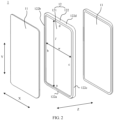
- FIG. 2 is an exploded view of the electronic device 1 shown in FIG. 1 .
- the electronic device 1 is a mobile phone.
- the electronic device 1 includes a display 11, a middle frame 12, and a back cover 13.
- the display 11 is configured to display an image, a video, and the like.
- the display 11 may be a flexible display, or may be a rigid display.
- the display 11 may be an organic light-emitting diode (organic light-emitting diode, OLED) display, an active-matrix organic light-emitting diode (active-matrix organic light-emitting diode, AMOLED) display, a mini light-emitting diode (mini organic light-emitting diode) display, a micro light-emitting diode (micro organic light-emitting diode) display, a micro organic light-emitting diode (micro organic light-emitting diode) display, a quantum dot light emitting diode (quantum dot light emitting diode, QLED) display, or a liquid crystal display (liquid crystal display, LCD).
- OLED organic light-emitting diode
- AMOLED active-matrix organic light-emit
- the back cover 13 forms a rear housing of the electronic device 1.
- the back cover 13 is configured to provide waterproof and dustproof protection for electronic components in the electronic device 1, and ensure appearance neatness of the electronic device 1.
- a forming material of the back cover 13 may be a conductive material such as metal, or may be a non-conductive material such as glass or plastic. When the forming material of the back cover 13 is a conductive material such as metal, the back cover 13 may be used as a reference ground for an electronic component or a radio frequency component in the electronic device.
- the middle frame 12 includes a middle plate 121 and a frame 122.
- the middle plate 121 is located between the display 11 and the back cover 13, and is stacked with the display 11 and the back cover 13 in a thickness direction (a Z direction shown in the figure) of the electronic device 1.
- a forming material of the middle plate 121 is a conductive material such as metal.
- the middle plate 121 is an approximately rectangular plate-shaped structure.
- the middle plate 121 has a first edge a and a fourth edge d that are opposite to each other, and a second edge b and a third edge c that are opposite to each other.
- the first edge a and fourth edge d are two shorter edges of the middle plate 121, and the second edge b and the third edge c are two longer edges of the middle plate 121.
- first edge a and the fourth edge d may alternatively be two longer edges of the middle plate 121, and in this case, the second edge b and the third edge c are two shorter edges of the middle plate 121.
- a length l of the middle plate 121 in an extension direction of the two longer edges is 150 mm ⁇ 10 mm
- a width w of the middle plate 121 in an extension direction of the two shorter edges is 75 mm ⁇ 5 mm.
- the extension direction of the two shorter edges of the middle plate 121 is defined as a transverse direction (an X direction shown in the figure)
- the extension direction of the two longer edges of the middle plate 121 is defined as a longitudinal direction (a Y direction shown in the figure).
- the frame 122 is disposed around the edges of the middle plate 121.
- the frame 122 includes a first side 122a, a second side 122b, a third side 122c, and a fourth side 122d.
- the first side 122a is disposed around the first edge a
- the second side 122b is disposed around the second edge b
- the third side 122c is disposed around the third edge c
- the fourth side 122d is disposed around the fourth edge d.
- the first side 122a, the second side 122b, the third side 122c, and the fourth side 122d are connected end to end to form the frame 122 with a square shape.
- the electronic device 1 is a square plate-shaped structure, in other words, the frame 122 is square.
- a forming material of the frame 122 may be a conductive material such as metal, or may be a non-conductive material such as plastic or resin.
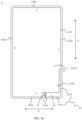
- FIG. 3a is a schematic diagram of an internal structure of the electronic device 1 shown in FIG. 1 .
- the electronic device 1 further includes an antenna 14, a first radio frequency front end 15, and a reference ground layer 23.
- the antenna 14 includes a first radiator 141.
- the first radiator 141 is configured to radiate a radio frequency signal to the outside and/or receive a radio frequency signal from the outside, so that the electronic device 1 can communicate with the outside through the antenna 14.
- the forming material of the frame 122 is a conductive material such as metal
- the frame 122 has a first gap A, and a part that is of the frame 122 and that is located on one side of the first gap A and adjacent to the first gap A forms the first radiator 141.
- a structural form of the first radiator 141 may include the following two implementations:
- the frame 122 further has a fourth gap D, and a part that is of the frame 122 and that is located between the first gap A and the fourth gap D forms the first radiator 141.
- the first gap A is disposed on the first side 122a
- the fourth gap D is disposed on the third side 122c.
- the first radiator 141 includes a third section 1411 and a fourth section 1412 that intersect.
- the third section 1411 is located between the first gap A and the fourth section 1412, and the third section 1411 is disposed around the first edge a of the middle plate 121.
- the fourth section 1412 is located between the third section 1411 and the fourth gap D, and the fourth section 1412 is disposed around the third edge c of the middle plate 121.
- a length of the fourth section 1412 is less than or equal to 1/2 times a length of the third side 122c. It may be understood that both the first gap A and the fourth gap D may be disposed on the first side 122a. This is not specifically limited herein.
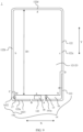
- FIG. 4a is a schematic diagram of another internal structure of the electronic device 1 shown in FIG. 1 .
- an end that is of the first radiator 141 and that is away from the first gap A is connected to another part of the frame 122.
- the end that is of the first radiator 141 and that is away from the first gap A is an end (corresponding to a K end in FIG. 4a ) that is of the first radiator 141 and that is farthest away from the first gap A in an extension direction of the first radiator 141.
- the first gap A is disposed on the first side 122a, and a part (namely, the K end) that is of the first radiator 141 and that is connected to the another part of the frame 122 is located on the third side 122c.
- the first radiator 141 includes a third section 1411 and a fourth section 1412 that intersect.
- the third section 1411 is located between the first gap A and the fourth section 1412, and the third section 1411 is disposed around the first edge a of the middle plate 121.
- the fourth section 1412 is located between the third section 1411 and the K end, and the fourth section 1412 is disposed around the third edge c of the middle plate 121.
- the first gap A and the fourth gap D may be filled with a dielectric material, to ensure structural integrity of the frame 122.
- another part of the frame 122 except the first radiator 141 may be obtained by being connected to the middle plate 121 and integrally formed.
- the clearance 16 may be filled with a dielectric material, to ensure structural integrity of the middle frame 12.
- the frame 122 when the forming material of the frame 122 is a non-conductive material such as plastic or resin, the frame 122 cannot form the first radiator 141, and the first radiator 141 may be disposed on an inner side of the frame 122 or embedded inside the frame 122.
- the frame 122 has a first frame segment, and the first radiator 141 is attached to the first frame segment or embedded inside the first frame segment.
- the first radiator 141 is attached to the first frame segment means that the first radiator 141 may be closely attached to the first frame segment, or may be disposed close to the first frame segment, in other words, there may be a specific small gap between the first radiator 141 and the first frame segment.
- the structural form of the first radiator 141 may be a flexible printed circuit (flexible printed circuit, FPC) form, a laser-direct-structuring (laser-direct-structuring, LDS) form, or a mode decoration antenna (mode decoration antenna, MDA) form. This is not specifically limited herein.
- the first radiator 141 has a first feed point 141a and a first ground point 141b that are disposed at an interval.
- the reference ground layer 23 is electrically connected to the first ground point 141b of the first radiator 141.
- the reference ground layer 23 is formed by the middle plate 121. It may be understood that the reference ground layer 23 may alternatively be formed by another structure in the electronic device 1, for example, a metal layer in a main board or the back cover 13 made of a conductive material such as metal.
- the reference ground layer 23 is electrically connected to the first ground point 141b through a connecting piece such as a spring or a conducting wire. In some other embodiments, still as shown in FIG.
- the first ground point 141b of the first radiator 141 is the end K of the first radiator 141, and the reference ground layer 23 is connected to the end K of the first radiator 141 through the frame 122, to implement a ground connection.
- the first ground point 141b in this application is not an actual point, and a location at which the reference ground layer 23 is electrically connected to the first radiator 141 through a ground piece or a part of the frame 122 is the first ground point 141b.
- the first radio frequency front end 15 is electrically connected to the first feed point 141a of the first radiator 141, and the first radio frequency front end 15 is configured to feed a radio frequency signal to the first radiator 141 and/or receive a radio frequency signal received by the first radiator 141 from the outside.
- the first radio frequency front end 15 includes a transmit channel and a receive channel.
- the transmit channel includes components such as a power amplifier and a filter.
- the components such as the power amplifier and the filter perform processing such as power amplification and filtering on a signal, transmit a processed signal to the first radiator 141, and transmit the processed signal to the outside through the first radiator 141.
- the receive channel includes components such as a low noise amplifier and a filter.
- the components such as the low noise amplifier and the filter perform processing such as low noise amplification and filtering on a signal received by the first radiator 141 from the outside, and then transmit a processed signal to a radio frequency chip, to implement communication between the electronic device 1 and the outside through the first radio frequency front end 15 and the antenna 14.
- the first feed point 141a in this application is not an actual point, and a location at which the first radio frequency front end 15 is electrically connected to the first radiator 141 is the first feed point 141a in this application.
- the first radio frequency front end 15 is disposed between the middle plate 121 of the middle frame 12 and the back cover 13.
- a frequency of the radio frequency signal fed by the first radio frequency front end 15 falls within the main resonant band of the first radiator 141.
- locations of disposing the first feed point 141a and the first ground point 141b on the first radiator 141 are not specifically limited, provided that the first feed point 141a and the first ground point 141b are disposed at an interval in the extension direction of the first radiator 141.
- the first feed point 141a is located between the first ground point 141b and the first gap A.
- the first feed point 141a is disposed close to the first gap A. That is, a distance between the first feed point 141a and the first gap A in the extension direction of the first radiator 141 is defined as a first distance, and a distance between the first feed point 141a and the first ground point 141b in the extension direction of the first radiator 141 is defined as a second distance. The first distance is less than the second distance.
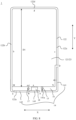
- FIG. 3b is a schematic diagram of a structure formed after the first feed point 141a is disposed close to the first ground point 141b in the electronic device 1 shown in FIG.
- the part that is of the first radiator 141 and that is located between the first gap A and the first ground point 141b forms an inverted-F (inverted-F antenna, IFA) antenna, and a resonant band of the IFA antenna is the main resonant band of the first radiator 141.
- IFA inverted-F antenna
- the first feed point 141a may alternatively be located on a side that is of the first ground point 141b and that is close to the fourth gap D, in other words, the first feed point 141a is located between the first ground point 141b and the fourth gap D.
- the first feed point 141a is disposed close to the first gap A. That is, a distance between the first feed point 141a and the first gap A in the extension direction of the first radiator 141 is defined as a first distance, and a distance between the first feed point 141a and the first ground point 141b in the extension direction of the first radiator 141 is defined as a second distance. The first distance is less than the second distance.
- the first radiator 141 forms a CRLH antenna, and a resonant band of the CRLH antenna is the main resonant band of the first radiator 141.
- FIG. 4b is a schematic diagram of a structure formed after the first feed point 141a is disposed close to the first ground point 141b in the electronic device 1 shown in FIG. 4a .
- a part that is of the first radiator 141 and that is located between the first gap A and the first ground point 141b forms an IFA antenna, and a resonant band of the IFA antenna is the main resonant band of the first radiator 141.
- the antenna in the electronic device 1 provided in this embodiment of this application transmits or receives a signal through the conductive frame 122, a conductive radiator disposed on an inner side of the non-conductive frame 122, or a conductive radiator embedded inside the non-conductive frame 122.
- a large screen such as a curved screen
- at least two opposite edges of the display 11 are bent toward the back cover 13, to form an electronic device with the curved screen
- FIG. 5 is a three-dimensional diagram of the electronic device 1 with the curved screen according to some embodiments of this application.
- edges of the display 11 ( FIG. 5 shows only opposite edges on two sides, and the edges may alternatively be peripheral edges) are bent toward the back cover 13.
- a dimension (namely, d1 in FIG. 5 ) of the frame 122 in a thickness direction (namely, a Z direction, where the Z direction is perpendicular to an X direction, and the Z direction is also perpendicular to a Y direction) of the electronic device 1 is smaller, and curved parts on two sides of the display 11 block the frame 122 in the thickness direction (namely, the Z direction in FIG. 5 ) of the electronic device, or the frame 122 is projected on the display 11 in the thickness direction (in other words, the display 11 is located on an orthographic projection area o n an XY plane). Consequently, the antenna implements signal radiation through the conductive frame 122, the conductive radiator disposed on the inner side of the non-conductive frame 122, or the conductive radiator embedded inside the non-conductive frame 122, resulting in low radiation efficiency.
- FIG. 6 is a schematic diagram of another internal structure of the electronic device 1 shown in FIG. 1 .
- the antenna 14 further includes a second radiator 142.
- the second radiator 142 and the first radiator 141 are disposed at an interval, and a signal on the first radiator 141 may be coupled to the second radiator 142.
- the reference ground layer 23 has a first edge, and a second edge and a third edge that are respectively connected to two ends of the first edge.
- the first edge a of the middle plate 121 forms the first edge of the reference ground layer 23
- the second edge b of the middle plate 121 forms the second edge of the reference ground layer 23
- the third edge c of the middle plate 121 forms the third edge of the reference ground layer 23.
- the first edge a of the middle plate 121, the second edge b of the middle plate 121, and the third edge c of the middle plate 121 respectively represent three sequentially connected side walls of the middle plate 121.
- the second radiator 142 is electrically connected to the first edge a of the middle plate 121, an end section that is of the second edge b and that is connected to the first edge a, or an end section that is of the third edge c and that is connected to the first edge a.
- the first edge a may be a straight edge, may be a cambered edge, or may be a wavy edge. This is not specifically limited herein.
- the first edge a has a first end M and a second end N.
- the first end M of the first edge a is an end that is of the first edge a and that is connected to the second edge b
- the second end N of the first edge a is an end that is of the first edge a and that is connected to the third edge c.
- the end section that is of the second edge b and that is connected to the first edge a is a section in which a distance to the first end M falls within a first preset length range, and the first preset length may be 1/2 times, 1/4 times, or 1/8 times a length of the second edge b. This is not specifically limited herein.
- the end section that is of the third edge c and that is connected to the first edge a is a section in which a distance between to the second end N falls within a second preset length range, and the second preset length may be 1/2 times, 1/4 times, or 1/8 times a length of the third edge c. This is not specifically limited herein.
- the second radiator 142 may alternatively be connected to an area in which a distance between a largest plane of the middle plate 121 and each of the first edge a, the end section that is of the second edge b and that is connected to the first edge a, and the end section that is of the third edge c and that is connected to the first edge is 50 mm.
- the forming material of the frame 122 is a conductive material such as metal.
- the frame 122 further has a second gap B and a third gap C.
- a part that is of the frame 122 and that is located between the second gap B and the third gap C forms the second radiator 142.
- a relative location relationship between each of the first gap A, the second gap B, and the third gap C and the first radiator 141 may include the following Embodiment 1 and Embodiment 2.
- Embodiment 1 Still as shown in FIG. 6 , the second gap B and the first gap A are a same gap, and the third gap C is located on a side that is of the second gap B and that is away from the first radiator 141. In other words, the first gap A and the second gap B are located between the third gap C and the first radiator 141. In this case, the second radiator 142 and the first radiator 141 are adjacent and disposed at an interval, and a distance between the second radiator 142 and the first radiator 141 is close, so that the antenna 14 has a compact structure, and occupies less space on the frame 122.
- the third gap C may also be filled with a dielectric material, to ensure structural integrity of the frame 122.
- the clearance 16 may be filled with a dielectric material, to ensure structural integrity of the middle frame 12.
- Embodiment 2 Refer to FIG. 7 to FIG. 9.
- FIG. 7 to FIG. 9 are schematic diagrams of other three internal structures of the electronic device 1 shown in FIG. 1 .
- the second gap B and the first gap A are disposed at an interval.
- the second gap B and the third gap C are located on a side that is of the first gap A and that is away from the first radiator 141.
- the first radiator 141 is located on a side of the first gap A
- the second gap B and the third gap C are located on the other side of the first gap A.
- the third gap C is located on a side that is of the second gap B and that is away from the first gap A, in other words, the second gap B is located between the third gap C and the first gap A.
- a part that is of the frame 122 and that is located between the second gap B and the first gap A forms a floating conductor 143. It may be understood that at least one gap may be added to the part that is of the frame 122 and that is between the second gap B and the first gap A, to form a plurality of floating conductors 143 between the second gap B and the first gap A.
- the floating conductor 143 is not connected to a reference ground (including the reference ground layer 23).
- the second radiator 142 When a radio frequency signal is fed at the first feed point 141a, the second radiator 142 can be indirectly coupled to the first radiator 141 through the floating conductor 143.
- at least one floating conductor 143 is spaced between the second radiator 142 and the first radiator 141.
- a location of the second radiator 142 may be adjusted to a location with a better clearance environment through the at least one floating conductor 143, so that the second radiator 142 is electrically connected to the first edge a of the middle plate 121.
- both the first gap A and the second gap B are disposed on the first side 122a of the frame 122.
- the first gap A and the second gap B are symmetrically disposed with respect to a center of the first side 122a. In this way, appearance effect of the frame 122 is better.
- a universal serial bus (universal serial bus, USB) device 18 is disposed on an inner side of the floating conductor 143 and is attached to the floating conductor 143.
- the inner side of the floating conductor 143 is a side that is of the floating conductor 143 and that faces the inside of the electronic device when the floating conductor 143 is applied to the electronic device.
- the second gap B is disposed closer to the first end M of the first edge a than the first gap A. That is, a distance between the first gap A and the first end M of the first edge a in an extension direction of the first side 122a is greater than a distance between the second gap B and the first end M of the first edge a in the extension direction of the first side 122a. It may be understood that the second gap B may alternatively be disposed closer to the second end N of the first edge a than the first gap A.
- a distance between the first gap A and the first end M of the first edge a in an extension direction of the first side 122a is less than a distance between the second gap B and the first end M of the first edge a in the extension direction of the first side 122a. This is not specifically limited herein.
- the third gap C may be disposed on the first side 122a of the frame 122, or may be disposed on the second side 122b of the frame 122. In some embodiments, still as shown in FIG. 7 , the third gap C is disposed on the first side 122a of the frame 122. In some other embodiments, FIG. 9 is a schematic diagram of another internal structure of the electronic device 1 shown in FIG. 1 . In this embodiment, the third gap C is disposed on the second side 122b of the frame 122. In this case, the second radiator 142 includes a first section 1421 and a second section 1422 that intersect.
- the first section 1421 is located between the second gap B and the second section 1422, and the first section 1421 is disposed around the first edge a of the middle plate 121.
- the second section 1422 is located between the first section 1421 and the third gap C, and the second section 1422 is disposed around the second edge b of the middle plate 121.
- a length of the second section 1422 is less than or equal to 1/4 times a length of the second side 122b.
- the second gap B and the third gap C may also be filled with a dielectric material, to ensure structural integrity of the frame 122.
- the clearances 16 may be filled with a dielectric material, to ensure structural integrity of the middle frame 12.
- the frame 122 when the forming material of the frame 122 is a non-conductive material such as plastic or resin, the frame 122 cannot form the second radiator 142 described in Embodiment 1 and Embodiment 2.
- the second radiator 142 may be disposed on an inner side of the frame 122 or embedded inside the frame 122.
- the frame 122 has a second frame segment, and the second radiator 142 is attached to the second frame segment or embedded inside the second frame segment. In this way, the second gap B and the third gap C do not need to be disposed on the frame 122, to ensure structural integrity of the frame 122.
- a structural form of the second radiator 142 may be a flexible printed circuit (flexible printed circuit, FPC) form, a laser-direct-structuring (laser-direct-structuring, LDS) form, or a mode decoration antenna (mode decoration antenna, MDA) form. This is not specifically limited herein.
- FPC flexible printed circuit
- LDS laser-direct-structuring
- MDA mode decoration antenna
- the reference ground layer 23 can be excited within a main resonant band of the first radiator 141 to generate a 1/2 wavelength characteristic mode in a first direction.
- an electrical length of the reference ground layer 23 in the first direction is a 1/2 wavelength of the main resonant band of the first radiator 141.
- the electrical length of the reference ground layer 23 in the first direction is a 1/2 wavelength of a main resonant frequency of 703 MHz to a 1/2 wavelength of a main resonant frequency of 803 MHz.
- the electrical length of the reference ground layer 23 in the first direction is a physical length (namely, mechanical length or geometric length) D1 of the reference ground layer 23 in the first direction multiplied by a ratio of time t 1 of transmitting an electrical or electromagnetic signal in the reference ground layer 23 in the first direction to time t 2 required for the signal to pass through a same distance in free space as the physical length of the reference ground layer 23 in the first direction.
- the electrical length of the reference ground layer 23 in the first direction may be a ratio of a physical length (namely, mechanical length or geometric length) D1 of the reference ground layer 23 in the first direction to a wavelength ⁇ of an electromagnetic wave transmitted by the reference ground layer 23.
- the first direction is parallel to a plane on which the reference ground layer 23 is located and perpendicular to an extension direction of the first edge a.
- the extension direction of the first edge a is parallel to the first edge a.
- the extension direction of the first edge a is consistent with an extension direction of a center line of the wavy edge.
- the center line of the wavy edge is a straight line passing through a middle section of the first edge part between any adjacent wave crest point and trough point of the wave edge.
- the middle section of the first edge part between the adjacent wave crest point and trough point is a section in which a central point of the middle section coincides with a central point of the first edge part, and a length of the middle section is 1/2 times, 3/5 times, or the like, a length of the first edge part.
- the first edge a is a cambered edge
- the extension direction of the first edge a is consistent with an approximately straight-line extension direction of the first edge a.
- An included angle between the approximately straight-line extension direction of the first edge a and any section on the first edge a is less than or equal to a first preset angle, and the first preset angle includes but is not limited to 15°, 20°, or 30°.
- the first edge a is a straight edge
- the first direction is a direction perpendicular to the first edge a.
- a parasitic resonant band generated by the second radiator 142 when a radio frequency signal is fed at the first feed point 141a is lower than a main resonant band of the first radiator 141.
- the parasitic resonant band generated by the second radiator 142 when the radio frequency signal is fed at the first feed point 141a is close to the main resonant band of the first radiator 141.
- the second radiator 142 is added, so that the parasitic resonant band generated through coupling between the second radiator 142 and the first radiator 141 when the radio frequency signal is fed at the first feed point 141a is lower than the main resonant band of the first radiator 141.
- the second radiator 142 is electrically connected to the first edge a of the reference ground layer 23, so that the electrical length of the reference ground layer 23 in the first direction is the 1/2 wavelength of the main resonant band of the first radiator 141, in other words, the reference ground layer 23 can be excited within the main resonant band of the first radiator 141 to generate the 1/2 wavelength characteristic mode in the first direction. In this way, the first radiator 141 is excited to generate resonance, and the second radiator 142 excites the reference ground layer 23, to improve radiation efficiency of the antenna 14.
- the second radiator 142 is electrically connected to the first edge a of the reference ground layer 23 through a lumped parameter element 17.
- the lumped parameter element 17 includes but is not limited to a capacitor, an inductor, or a circuit obtained by connecting one or two of an inductor or a capacitor in parallel, in series, or in series-parallel.
- the lumped parameter element 17 is an inductor, and an inductance value of the inductor may be 18 nH.
- an electrical length of the second radiator 142 is adjusted through the lumped parameter element 17, to reduce a physical length of the second radiator 142 while adjusting the parasitic resonant band generated by the second radiator 142 when the radio frequency signal is fed at the first feed point 141a to be lower than the main resonant band of the first radiator 141. Therefore, an occupation length of the antenna 14 on the frame 122 can be reduced.
- the second radiator 142 is electrically connected to the first edge a of the middle plate 121.
- the second radiator 142 may be electrically connected to a middle section of the first edge a of the middle plate 121, or the second radiator 142 may be electrically connected to an end section of the first edge a of the middle plate 121. This is not specifically limited herein.
- the second radiator 142 is electrically connected to the middle section of the first edge a of the middle plate 121.
- the middle section of the first edge a is a section in which a distance to a center point of the first edge a falls within a third preset length range, and the third preset length may be 1/4 times, 1/10 times, or 1/8 times a length of the first edge a.
- the second radiator 142 is electrically connected to the end section of the first edge a of the middle plate 121.
- the end section of the first edge a is a section in which a distance to the first end M or the second end N of the first edge a falls within a fourth preset length range.
- the second end N is an end that is of the first edge a and that is opposite to the first end M.
- the fourth preset length may be 1/2 times the length of the first edge a. In this way, when the second radiator 142 excites the reference ground layer 23, a first direction mode (namely, longitudinal mode) of the reference ground layer 23 is fully excited, so that radiation efficiency of the antenna 14 can be further improved.
- a first direction mode namely, longitudinal mode
- the second gap B is disposed closer to the first end M of the first edge a than the first gap A, and the second radiator 142 is electrically connected to an end section in which the first end M of the first edge a is located.
- the end section in which the first end M is located is a section in which a distance between to the first end M of the first edge a falls within the fourth preset length range. Because a distance between the end section in which the first end M is located and the second radiator 142 is short, an electrical connection path between the second radiator 142 and the end section in which the first end M is located is short. This facilitates wiring.
- the second radiator 142 is electrically connected to the end section in which the first end M of the first edge a is located, for example, as shown in FIG.
- the second radiator 142 is electrically connected to a first end M location of the end section in which the first end M is located.
- the second radiator 142 is electrically connected to a m1 location of the end section in which the first end M is located.
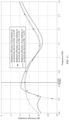
- FIG. 10 is a curve comparison diagram of radiation efficiency at which the antennas 14 in the electronic devices 1 shown in FIG. 3a , FIG. 6 , FIG. 7 , and FIG. 8 generate an antenna band of B28 (namely, 703 MHz to 803 MHz) in a free space (FS) state.
- FIG. 11 is a curve comparison diagram of radiation efficiency at which the antennas 14 in the electronic devices 1 shown in FIG. 3a , FIG. 6 , and FIG. 7 generate an antenna band of B5 (namely, 824 MHz to 894 MHz) in an FS state.
- FIG. 12 is a curve comparison diagram of radiation efficiency at which the antennas 14 in the electronic devices 1 shown in FIG. 3a , FIG. 6 , and FIG.
- the second radiator 142 is added to the antennas 14 in the electronic devices 1 shown in FIG. 6 , FIG. 7 , and FIG. 8 , and the second radiator 142 is electrically connected to the first edge a of the middle plate 121.
- the second radiator 142 of the antenna 14 is electrically connected to the middle section of the first edge a of the middle plate 121.
- the second radiator 142 of the antenna 14 is electrically connected to the end section in which the first end M of the first edge a of the middle plate 121 is located.
- an abscissa is a frequency (where a unit is GHz) and an ordinate is efficiency (where a unit is dB).
- a common low band (low band, LB) antenna band for example, a band of B28, B5, or B8 in an FS state is greater than radiation efficiency at which the antenna 14 in the electronic device 1 shown in FIG.
- FIG. 13 is a schematic diagram of another internal structure of the electronic device 1 shown in FIG. 1 .
- the second radiator 142 has a second ground point 142b and a second feed point 142a that are disposed at an interval. Locations of disposing the second ground point 142b and the second feed point 142a on the second radiator 142 are not limited, provided that the second ground point 142b and the second feed point 142a are disposed at an interval along the second radiator 142.
- the second ground point 142b and the second feed point 142a are respectively disposed at opposite ends of the second radiator 142 in an extension direction of the second radiator 142. For example, still as shown in FIG.
- the second ground point 142b is disposed at an end that is of the second radiator 142 and that forms the third gap C
- the second feed point 142a is disposed at an end that is of the second radiator 142 and that forms the second gap B.
- the second ground point 142b may alternatively be disposed at an end that is of the second radiator 142 and that forms the second gap B
- the second feed point 142a is disposed at an end that is of the second radiator 142 and that forms the third gap C.
- the second radiator 142 forms a CRLH antenna or a loop (loop) antenna.
- FIG. 14 is a diagram of an enlarged part of the electronic device 1 shown in FIG. 13 .
- the second ground point 142b is electrically connected to the reference ground layer 23 through a filter 19.
- the second ground point 142b is electrically connected to one end of the filter 19, and the other end of the filter 19 is electrically connected to the reference ground layer 23.
- the filter 19 is an LC filter.
- the filter 19 includes a capacitor C and an inductor L that are connected in parallel. The filter 19 is configured to prevent a signal within the first band from passing through and allow a signal within the second band to pass through.
- the first band includes a main resonant band generated by the first radiator 141 and a parasitic resonant band generated by the second radiator 142 when a radio frequency signal is fed at the first feed point 141a.
- the first band includes a minimum frequency value within the parasitic resonant band generated by the second radiator 142 when the radio frequency signal is fed at the first feed point 141a to a maximum frequency value within the main resonant band generated by the first radiator 141 when the radio frequency signal is fed at the first feed point 141a.
- the parasitic resonant band generated by the second radiator 142 when the radio frequency signal is fed at the first feed point 141a is 700 MHz to 750 MHz
- the minimum frequency value within the band is 700 MHz
- the main resonant band generated by the first radiator 141 when the radio frequency signal is fed at the first feed point 141a is 780 MHz to 850 MHz
- the maximum frequency value within the band is 850 MHz.
- the first band includes 700 MHz to 850 MHz.
- the second band includes a main resonant band generated by the second radiator 142 when a radio frequency signal is fed at the second feed point 142a.
- the main resonant band generated by the second radiator 142 when the radio frequency signal is fed at the second feed point 142a is 1810 MHz to 2000 MHz
- the second band includes 1810 MHz to 2000 MHz.
- the first band includes the main resonant band generated by the first radiator 141 and the parasitic resonant band generated by the second radiator 142 when the radio frequency signal is fed at the first feed point 141a.
- the second band includes the main resonant band generated by the second radiator 142 when the radio frequency signal is fed at the second feed point 142a of the second radiator 142.
- FIG. 15 is a diagram of another enlarged part of the electronic device 1 shown in FIG. 13 .
- the second ground point 142b is electrically connected to the reference ground layer 23 through a switch circuit 21.
- the second ground point 142b is electrically connected to one end of the switch circuit 21, and the other end of the switch circuit 21 is electrically connected to the reference ground layer 23.
- the switch circuit 21 may be switched to an off state when the radio frequency signal within the first band is fed at the first feed point 141a, or may be in an on state when the radio frequency signal within the second band is fed at the second feed point 142a, to prevent the signal within the first band from passing through and allow the signal within the second band to pass through.
- the switch circuit 21 includes one active switch and tuning elements connected between the active switch and the second ground point 142b and/or between the active switch and the reference ground layer 23.
- the tuning element is an inductor, a capacitor, or a circuit obtained by connecting one or two of an inductor or a capacitor in parallel, in series, or in series-parallel.
- the switch circuit 21 includes a first switching switch 211 and a plurality of different first tuning elements 212.
- the first tuning element 212 includes but is not limited to a capacitor, an inductor, or a circuit obtained by connecting one or two of an inductor or a capacitor in parallel, in series, or in series-parallel.
- the plurality of first tuning elements 212 are electrically connected to the reference ground layer 23.
- the first switching switch 211 includes but is not limited to a single-pole multi-throw switch or a multi-pole multi-throw switch.
- the first switching switch 211 is configured to: when the radio frequency signal within the first band is fed at the first feed point 141a, disconnect an electrical connection path between the second ground point 142b and the plurality of first tuning elements 212; or when the radio frequency signal within the second band is fed at the second feed point, electrically connect the different first tuning elements to the second ground point in a switchable manner, to adjust the resonant band generated by the second radiator 142.
- the switch circuit 21 can prevent the signal within the first band from passing through and allow the signal within the second band to pass through.
- the switch circuit 21 may further adjust an operating band of the second radiator 142.
- the second ground point 142b in this application is not an actual point, and a location at which the reference ground layer 23 is electrically connected to the second radiator 142 through the filter 19 or the switch circuit 21 is the second ground point 142b.
- the electronic device 1 further includes a second radio frequency front end 20.
- the second radio frequency front end 20 is electrically connected to the second feed point 142a of the second radiator 142, and the second radio frequency front end 20 is configured to feed a radio frequency signal to the second radiator 142 or receive a radio frequency signal received by the second radiator 142 from the outside.
- the second radio frequency front end 20 includes a transmit channel and a receive channel.
- the transmit channel includes components such as a power amplifier and a filter.
- the components such as the power amplifier and the filter perform processing such as power amplification and filtering on a signal, transmit a processed signal to the second radiator 142, and transmit the processed signal to the outside through the second radiator 142.
- the receive channel includes components such as a low noise amplifier and a filter.
- the components such as the low noise amplifier and the filter perform processing such as low noise amplification and filtering on a signal received by the second radiator 142 from the outside, and then transmit a processed signal to a radio frequency chip, to implement communication between the electronic device 1 and the outside through the second radio frequency front end 20 and the antenna 14.
- the second feed point 142a in this application is not an actual point, and a location at which the second radio frequency front end 20 is electrically connected to the second radiator 142 is the second feed point 142a in this application.
- the second radio frequency front end 20 is disposed between the middle plate 121 of the middle frame 12 and the back cover 13.
- a frequency of the radio frequency signal fed by the second radio frequency front end 20 falls within the main resonant band of the second radiator 142.
- the antenna 1 provided in this embodiment can transmit or receive the signal within the first band when the radio frequency signal is fed at the first feed point 141a, and can further transmit or receive the signal within the second band when the radio frequency signal is fed at the second feed point 142a. Therefore, the antenna 14 has more application bands and a wide application range.
- the electronic device 1 is a mobile phone.
- a length of the middle plate 121 in a longitudinal direction is 150 mm ⁇ 10 mm, and a width of the middle plate 121 in a transverse direction is 75 mm ⁇ 5 mm.
- the first direction is consistent with the longitudinal direction of the middle plate 121, and a shorter edge of the middle plate 121 forms the first edge of the reference ground layer 23.
- the first band falls within a low band (low band, LB), and the second band falls within a medium/high band (middle/high band, MHB).
- the LB band may be, for example, 699 MHz to 960 MHz.
- the MHB band may be, for example, 1710 MHz to 2690 MHz.
- the antenna 14 provided in this embodiment of this application can cover a low/middle/high band (low/middle/high band, LMH), and has a wide application range.
- the electronic device 1 is a mobile phone.
- a length of the middle plate 121 in a longitudinal direction is 150 mm ⁇ 10 mm, and a width of the middle plate 121 in a transverse direction is 75 mm ⁇ 5 mm.
- the first direction is consistent with the transverse direction of the middle plate 121, and a longer edge of the middle plate 121 forms the first edge of the reference ground layer 23.
- the first band falls within a medium/high band (middle/high band, MHB), and the second band falls within an LB band.
- the lumped parameter element 17 is configured to adjust the electrical length of the second radiator 142, so that the second radiator 142 excites a first direction mode (for example, longitudinal mode) of the reference ground layer 23.
- the switch circuit 21 or the filter 19 When the radio frequency signal is fed at the second feed point 142a, the switch circuit 21 or the filter 19 is in an on state, the second ground point 142b of the second radiator 142 is connected to the reference ground layer 23, and the second radiator 142 is further connected to the first edge a of the reference ground layer 23 only through the lumped parameter element 17.
- the lumped parameter element 17 forms a tuning element of the second radiator 142, and the tuning element is configured to adjust an operating band of the second radiator 142.
- An end that is of the lumped parameter element 17 and that is connected to the second radiator 142 may be connected to an end part of the second radiator 142 in the extension direction of the second radiator 142, or may be connected to a middle part of the second radiator 142 in the extension direction of the second radiator 142. This is not specifically limited herein.
- both the lumped parameter element 17 and the second radio frequency front end 20 are connected to the second feed point 142a of the second radiator 142.
- the lumped parameter element 17 is electrically connected to the end part of the second radiator 142, and the lumped parameter element 17 and the second radio frequency front end 20 share a location on the second radiator 142. Therefore, a quantity of electrical connection points of the second radiator 142 can be reduced, and structural complexity is low.
- the third gap C is disposed on the second side 122b of the frame 122.
- the third gap C is easily blocked.
- MBB medium/high band
- FIG. 16 is a curve diagram of medium/high band input return loss coefficients (S11) (in other words, input return loss coefficients at the second feed point 142a) of the antenna 14 in the electronic device 1 shown in FIG. 13 in an FS state, a beside head hand left (beside head hand left, BHHL) state, and a beside head hand right (beside head hand right, BHHR) state.
- S11 medium/high band input return loss coefficients
- FIG. 18 is a curve diagram of medium/high band input return loss coefficients (S11) of the antenna 14 in the electronic device 1 shown in FIG. 17 in an FS state, a BHHL state, and a BHHR state.
- S11 medium/high band input return loss coefficients
- an abscissa is a frequency (where a unit is GHz) and an ordinate is S 11 (where a unit is dB). It can be learned, by comparing FIG. 16 with FIG. 18 , that the antenna 14 in the electronic device 1 shown in FIG.
- FIG. 19 is a curve comparison diagram of medium/high band radiation efficiency of the antennas 14 in the electronic devices shown in FIG. 13 and FIG. 17 in an FS state, a BHHL state, and a BHHR state.
- an abscissa is a frequency (where a unit is GHz) and an ordinate is radiation efficiency (where a unit is dB). It can be seen from FIG. 19 that the medium/high band radiation efficiency of the antenna 14 in the electronic device 1 shown in FIG.
- the antenna 14 in the electronic device 1 shown in FIG. 13 may be put into practical application, and the medium/high band radiation performance is good.
- FIG. 20 is a schematic diagram of another internal structure of the electronic device 1 shown in FIG. 1 .
- a part of the frame 122 that is located on a side of the third gap C and that is away from the second gap B and adjacent to the third gap C forms a third radiator 144, in other words, the third radiator 144 and the second radiator 142 are respectively located on two sides of the third gap C.
- the second radiator 142 is formed on the frame 122 and located on one side of the third gap C
- the third radiator 144 is formed on the frame 122 and located on the other side of the third gap C.
- the third radiator 144 may be coupled to the second radiator 142 to generate parasitic resonance when a radio frequency signal is fed at the second feed point 142a, so that a quantity of radiation bands of the antenna 14 can be further increased.
- FIG. 21 is a schematic diagram of another internal structure of the electronic device 1 shown in FIG. 1 .
- the third radiator 144 has a third ground point 144b and a third feed point 144a that are disposed at an interval.
- the third ground point 144b is electrically connected to the reference ground layer 23.
- the third ground point 144b is connected to another part of the frame 122b, so that the third ground point 144b is electrically connected to the middle plate 121 (namely, the reference ground layer 23) through the another part of the frame 122, to implement grounding.
- the electronic device 1 further includes a third radio frequency front end 22.
- the third radio frequency front end 22 is electrically connected to the third feed point 144a.
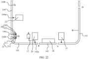
- FIG. 22 is a schematic diagram of another internal structure of the electronic device 1 shown in FIG. 1 .
- the third radiator 144 has a connection point 144c.
- the connection point 144c and the third ground point 144b are respectively located on two sides of the third feed point 144a.
- the connection point 144c is located at an end that is of the third radiator 144 and that is adjacent to the third gap C.
- the connection point 144c is electrically connected to the reference ground layer 23 through a switching circuit 24.
- the switching circuit 24 includes a second switching switch 241 and a plurality of different second tuning elements 242.
- the second tuning element 242 includes but is not limited to a capacitor, an inductor, or a circuit obtained by connecting one or two of an inductor or a capacitor in parallel, in series, or in series-parallel.
- the plurality of second tuning elements 242 are electrically connected to the reference ground layer 23.
- the second switching switch 241 includes but is not limited to a single-pole multi-throw switch or a multi-pole multi-throw switch.
- the second switching switch 241 is configured to electrically connect the different second tuning elements 242 to the connection point 144c in a switchable manner, to adjust a resonant frequency of the third radiator 144.
- the switching circuit 24 is configured to tune a resonant frequency of a part that is of the third radiator 144 and that is located between the third ground point 144b and the third gap C. It should be noted that the connection point 144c in this application is not an actual point, and a location at which the switching circuit 24 is electrically connected to the third radiator 144 is the connection point 144c.
- the first switching switch 211 in the switch circuit 21 and the second switching switch 241 in the switching circuit 24 are packaged together, and an entire switch line of a switch formed through package is a superposition of a switch line of the first switching switch 211 and a switch line of the second switching switch 241. Therefore, a quantity of components included in the electronic device can be reduced, and an assembly process of the electronic device can be simplified.
Landscapes
- Engineering & Computer Science (AREA)
- Computer Networks & Wireless Communication (AREA)
- Signal Processing (AREA)
- Support Of Aerials (AREA)
Applications Claiming Priority (2)
| Application Number | Priority Date | Filing Date | Title |
|---|---|---|---|
| CN202011507812.7A CN114649680B (zh) | 2020-12-18 | 2020-12-18 | 一种电子设备 |
| PCT/CN2021/139063 WO2022127896A1 (zh) | 2020-12-18 | 2021-12-17 | 一种电子设备 |
Publications (2)
| Publication Number | Publication Date |
|---|---|
| EP4239796A1 true EP4239796A1 (de) | 2023-09-06 |
| EP4239796A4 EP4239796A4 (de) | 2024-05-01 |
Family
ID=81989651
Family Applications (1)
| Application Number | Title | Priority Date | Filing Date |
|---|---|---|---|
| EP21905822.9A Pending EP4239796A4 (de) | 2020-12-18 | 2021-12-17 | Elektronische vorrichtung |
Country Status (4)
| Country | Link |
|---|---|
| US (1) | US12463324B2 (de) |
| EP (1) | EP4239796A4 (de) |
| CN (2) | CN120414082A (de) |
| WO (1) | WO2022127896A1 (de) |
Families Citing this family (7)
| Publication number | Priority date | Publication date | Assignee | Title |
|---|---|---|---|---|
| CN114466094B (zh) * | 2022-04-01 | 2022-09-09 | 荣耀终端有限公司 | 中框组件、其制备方法及电子设备 |
| US12424760B2 (en) * | 2022-07-29 | 2025-09-23 | Mediatek Inc. | Antenna |
| CN117673752A (zh) * | 2022-08-29 | 2024-03-08 | Oppo广东移动通信有限公司 | 天线组件及电子设备 |
| CN116259953A (zh) * | 2023-01-20 | 2023-06-13 | 华为技术有限公司 | 一种天线结构和电子设备 |
| CN116053760A (zh) * | 2023-01-20 | 2023-05-02 | 华为技术有限公司 | 一种电子设备 |
| WO2025026088A1 (zh) * | 2023-07-31 | 2025-02-06 | 华为技术有限公司 | 一种电子设备 |
| CN119518285B (zh) * | 2024-11-25 | 2025-12-02 | Oppo广东移动通信有限公司 | 电子设备 |
Family Cites Families (16)
| Publication number | Priority date | Publication date | Assignee | Title |
|---|---|---|---|---|
| JP2010245724A (ja) * | 2009-04-03 | 2010-10-28 | Mitsumi Electric Co Ltd | アンテナ装置 |
| KR102226173B1 (ko) * | 2014-09-02 | 2021-03-10 | 삼성전자주식회사 | 외부 금속 프레임을 이용한 안테나 및 이를 구비한 전자 장치 |
| KR102518499B1 (ko) * | 2016-04-22 | 2023-04-05 | 삼성전자주식회사 | 안테나 및 이를 포함하는 전자 장치 |
| CN105977634B (zh) * | 2016-05-03 | 2019-07-05 | 瑞声科技(新加坡)有限公司 | 一种lte全频带手机天线结构 |
| CN107871931B (zh) * | 2016-09-26 | 2021-06-15 | 深圳富泰宏精密工业有限公司 | 天线结构及具有该天线结构的无线通信装置 |
| CN108511905B (zh) * | 2018-04-19 | 2021-03-02 | Oppo广东移动通信有限公司 | 天线系统和移动终端 |
| CN108631041B (zh) * | 2018-04-25 | 2020-04-03 | Oppo广东移动通信有限公司 | 天线组件及电子装置 |
| CN110556620B (zh) * | 2018-06-01 | 2021-07-09 | 华为技术有限公司 | 天线及移动终端 |
| CN108767450B (zh) * | 2018-06-25 | 2021-06-22 | 维沃移动通信有限公司 | 一种天线系统及终端 |
| CN108736130B (zh) | 2018-07-11 | 2020-01-14 | Oppo广东移动通信有限公司 | 天线组件以及电子设备 |
| CN109687111B (zh) * | 2018-12-29 | 2021-03-12 | 维沃移动通信有限公司 | 一种天线结构及通信终端 |
| KR102606484B1 (ko) * | 2019-01-25 | 2023-11-27 | 삼성전자주식회사 | 안테나 장치를 포함하는 전자 장치 |
| CN111628298B (zh) * | 2019-02-27 | 2022-03-11 | 华为技术有限公司 | 共体天线及电子设备 |
| CN114824836B (zh) * | 2019-02-27 | 2025-04-08 | 华为技术有限公司 | 共体天线及电子设备 |
| CN110165373B (zh) | 2019-05-14 | 2021-09-24 | 荣耀终端有限公司 | 天线装置及电子设备 |
| CN117810676B (zh) | 2020-01-17 | 2024-10-11 | 荣耀终端有限公司 | 天线结构及具有该天线结构的电子设备 |
-
2020
- 2020-12-18 CN CN202510323799.6A patent/CN120414082A/zh active Pending
- 2020-12-18 CN CN202011507812.7A patent/CN114649680B/zh active Active
-
2021
- 2021-12-17 US US18/258,158 patent/US12463324B2/en active Active
- 2021-12-17 WO PCT/CN2021/139063 patent/WO2022127896A1/zh not_active Ceased
- 2021-12-17 EP EP21905822.9A patent/EP4239796A4/de active Pending
Also Published As
| Publication number | Publication date |
|---|---|
| CN114649680A (zh) | 2022-06-21 |
| CN120414082A (zh) | 2025-08-01 |
| CN114649680B (zh) | 2025-04-04 |
| WO2022127896A1 (zh) | 2022-06-23 |
| US20240055762A1 (en) | 2024-02-15 |
| EP4239796A4 (de) | 2024-05-01 |
| US12463324B2 (en) | 2025-11-04 |
Similar Documents
| Publication | Publication Date | Title |
|---|---|---|
| US12463324B2 (en) | Electronic device | |
| US12407113B2 (en) | Antenna assembly and electronic device | |
| EP4311024A1 (de) | Antennenanordnung und elektronische vorrichtung | |
| US12212052B2 (en) | Antenna and electronic device | |
| CN110544815B (zh) | 电子设备宽带天线 | |
| TWI425713B (zh) | 諧振產生之三頻段天線 | |
| WO2021023182A1 (zh) | 天线模组及电子设备 | |
| TW202205734A (zh) | 訊號饋入元件,天線模組及電子設備 | |
| CN112397898A (zh) | 天线阵列组件及电子设备 | |
| KR20250108121A (ko) | 안테나 구조, 안테나 모듈, 칩 및 전자 디바이스 | |
| CN112531340A (zh) | 一种电子设备 | |
| CN119495932B (zh) | 电池盖组件和电子设备 | |
| EP3787113B1 (de) | Antennenmodul und endgerät | |
| EP4557515A1 (de) | Antennenanordnung und elektronische vorrichtung | |
| US7598912B2 (en) | Planar antenna structure | |
| CN118281563A (zh) | 天线组件及电子设备 | |
| CN119481669A (zh) | 电子设备 | |
| WO2025256092A1 (zh) | 一种通信终端 | |
| CN118198723A (zh) | 天线组件及电子设备 | |
| CN119050650A (zh) | 天线组件及电子设备 | |
| CN119518269A (zh) | 电子设备 | |
| CN120149808A (zh) | 天线模组以及电子设备 | |
| WO2024179404A1 (zh) | 一种天线结构和电子设备 | |
| HK40102508A (en) | Antenna structure, antenna module, chip, and electronic device | |
| CN120657446A (zh) | 天线组件和电子设备 |
Legal Events
| Date | Code | Title | Description |
|---|---|---|---|
| STAA | Information on the status of an ep patent application or granted ep patent |
Free format text: STATUS: THE INTERNATIONAL PUBLICATION HAS BEEN MADE |
|
| PUAI | Public reference made under article 153(3) epc to a published international application that has entered the european phase |
Free format text: ORIGINAL CODE: 0009012 |
|
| STAA | Information on the status of an ep patent application or granted ep patent |
Free format text: STATUS: REQUEST FOR EXAMINATION WAS MADE |
|
| 17P | Request for examination filed |
Effective date: 20230602 |
|
| AK | Designated contracting states |
Kind code of ref document: A1 Designated state(s): AL AT BE BG CH CY CZ DE DK EE ES FI FR GB GR HR HU IE IS IT LI LT LU LV MC MK MT NL NO PL PT RO RS SE SI SK SM TR |
|
| DAV | Request for validation of the european patent (deleted) | ||
| DAX | Request for extension of the european patent (deleted) | ||
| REG | Reference to a national code |
Ref country code: DE Ref legal event code: R079 Free format text: PREVIOUS MAIN CLASS: H01Q0005100000 Ipc: H01Q0001240000 |
|
| A4 | Supplementary search report drawn up and despatched |
Effective date: 20240405 |
|
| RIC1 | Information provided on ipc code assigned before grant |
Ipc: H01Q 7/00 20060101ALN20240328BHEP Ipc: H01Q 9/42 20060101ALN20240328BHEP Ipc: H01Q 21/28 20060101ALI20240328BHEP Ipc: H01Q 5/378 20150101ALI20240328BHEP Ipc: H01Q 5/328 20150101ALI20240328BHEP Ipc: H01Q 1/48 20060101ALI20240328BHEP Ipc: H01Q 1/24 20060101AFI20240328BHEP |