EP4239694B1 - Hybrid-leuchtdiode und verfahren zur herstellung davon - Google Patents
Hybrid-leuchtdiode und verfahren zur herstellung davon Download PDFInfo
- Publication number
- EP4239694B1 EP4239694B1 EP23152548.6A EP23152548A EP4239694B1 EP 4239694 B1 EP4239694 B1 EP 4239694B1 EP 23152548 A EP23152548 A EP 23152548A EP 4239694 B1 EP4239694 B1 EP 4239694B1
- Authority
- EP
- European Patent Office
- Prior art keywords
- sublayer
- layer
- light emitting
- tunnel junction
- doped
- Prior art date
- Legal status (The legal status is an assumption and is not a legal conclusion. Google has not performed a legal analysis and makes no representation as to the accuracy of the status listed.)
- Active
Links
Images

Classifications
-
- H—ELECTRICITY
- H10—SEMICONDUCTOR DEVICES; ELECTRIC SOLID-STATE DEVICES NOT OTHERWISE PROVIDED FOR
- H10H—INORGANIC LIGHT-EMITTING SEMICONDUCTOR DEVICES HAVING POTENTIAL BARRIERS
- H10H20/00—Individual inorganic light-emitting semiconductor devices having potential barriers, e.g. light-emitting diodes [LED]
- H10H20/01—Manufacture or treatment
- H10H20/011—Manufacture or treatment of bodies, e.g. forming semiconductor layers
- H10H20/013—Manufacture or treatment of bodies, e.g. forming semiconductor layers having light-emitting regions comprising only Group III-V materials
- H10H20/0137—Manufacture or treatment of bodies, e.g. forming semiconductor layers having light-emitting regions comprising only Group III-V materials the light-emitting regions comprising nitride materials
-
- H—ELECTRICITY
- H10—SEMICONDUCTOR DEVICES; ELECTRIC SOLID-STATE DEVICES NOT OTHERWISE PROVIDED FOR
- H10H—INORGANIC LIGHT-EMITTING SEMICONDUCTOR DEVICES HAVING POTENTIAL BARRIERS
- H10H20/00—Individual inorganic light-emitting semiconductor devices having potential barriers, e.g. light-emitting diodes [LED]
- H10H20/80—Constructional details
- H10H20/81—Bodies
- H10H20/811—Bodies having quantum effect structures or superlattices, e.g. tunnel junctions
-
- G—PHYSICS
- G09—EDUCATION; CRYPTOGRAPHY; DISPLAY; ADVERTISING; SEALS
- G09F—DISPLAYING; ADVERTISING; SIGNS; LABELS OR NAME-PLATES; SEALS
- G09F9/00—Indicating arrangements for variable information in which the information is built-up on a support by selection or combination of individual elements
- G09F9/30—Indicating arrangements for variable information in which the information is built-up on a support by selection or combination of individual elements in which the desired character or characters are formed by combining individual elements
- G09F9/33—Indicating arrangements for variable information in which the information is built-up on a support by selection or combination of individual elements in which the desired character or characters are formed by combining individual elements being semiconductor devices, e.g. diodes
-
- H—ELECTRICITY
- H10—SEMICONDUCTOR DEVICES; ELECTRIC SOLID-STATE DEVICES NOT OTHERWISE PROVIDED FOR
- H10D—INORGANIC ELECTRIC SEMICONDUCTOR DEVICES
- H10D62/00—Semiconductor bodies, or regions thereof, of devices having potential barriers
- H10D62/80—Semiconductor bodies, or regions thereof, of devices having potential barriers characterised by the materials
- H10D62/86—Semiconductor bodies, or regions thereof, of devices having potential barriers characterised by the materials being Group II-VI materials, e.g. ZnO
- H10D62/864—Semiconductor bodies, or regions thereof, of devices having potential barriers characterised by the materials being Group II-VI materials, e.g. ZnO further characterised by the dopants
-
- H—ELECTRICITY
- H10—SEMICONDUCTOR DEVICES; ELECTRIC SOLID-STATE DEVICES NOT OTHERWISE PROVIDED FOR
- H10H—INORGANIC LIGHT-EMITTING SEMICONDUCTOR DEVICES HAVING POTENTIAL BARRIERS
- H10H20/00—Individual inorganic light-emitting semiconductor devices having potential barriers, e.g. light-emitting diodes [LED]
- H10H20/80—Constructional details
- H10H20/81—Bodies
- H10H20/822—Materials of the light-emitting regions
- H10H20/824—Materials of the light-emitting regions comprising only Group III-V materials, e.g. GaP
- H10H20/825—Materials of the light-emitting regions comprising only Group III-V materials, e.g. GaP containing nitrogen, e.g. GaN
-
- H—ELECTRICITY
- H10—SEMICONDUCTOR DEVICES; ELECTRIC SOLID-STATE DEVICES NOT OTHERWISE PROVIDED FOR
- H10H—INORGANIC LIGHT-EMITTING SEMICONDUCTOR DEVICES HAVING POTENTIAL BARRIERS
- H10H20/00—Individual inorganic light-emitting semiconductor devices having potential barriers, e.g. light-emitting diodes [LED]
- H10H20/80—Constructional details
- H10H20/84—Coatings, e.g. passivation layers or antireflective coatings
-
- H—ELECTRICITY
- H10—SEMICONDUCTOR DEVICES; ELECTRIC SOLID-STATE DEVICES NOT OTHERWISE PROVIDED FOR
- H10H—INORGANIC LIGHT-EMITTING SEMICONDUCTOR DEVICES HAVING POTENTIAL BARRIERS
- H10H20/00—Individual inorganic light-emitting semiconductor devices having potential barriers, e.g. light-emitting diodes [LED]
- H10H20/80—Constructional details
- H10H20/85—Packages
- H10H20/851—Wavelength conversion means
- H10H20/8511—Wavelength conversion means characterised by their material, e.g. binder
- H10H20/8512—Wavelength conversion materials
-
- H—ELECTRICITY
- H10—SEMICONDUCTOR DEVICES; ELECTRIC SOLID-STATE DEVICES NOT OTHERWISE PROVIDED FOR
- H10H—INORGANIC LIGHT-EMITTING SEMICONDUCTOR DEVICES HAVING POTENTIAL BARRIERS
- H10H29/00—Integrated devices, or assemblies of multiple devices, comprising at least one light-emitting semiconductor element covered by group H10H20/00
- H10H29/10—Integrated devices comprising at least one light-emitting semiconductor component covered by group H10H20/00
Definitions
- the present invention relates to a hybrid light emitting diode emitting single photons and a method of fabrication of a hybrid light emitting diode emitting single photons.
- Sources of single photons containing a photon emitter in the form of a two-dimensional semiconductor transition metal dichalcogenide (2D TMD) layer excited by laser light, are applied widely in telecommunication for quantum key distribution in secure encrypted connections.
- Emitters of single photons in the form of a two-dimensional semiconductor layer of tungsten diselenide (WSe 2 ), which, when excited by an external light with the wavelength of 400-550 nm, can emit single photons with the wavelength of 650-750 nm, are disclosed, among others, in the article by K.F. Mak and J. Shan titled "Photonics and optoelectronics of 2D semiconductor transition metal dichalcogenides" [Nature Photonics, vol. 10, pp.
- US 2019/363514 A1 discloses a LED device comprising a WSe2 layer as a LED pumped nano cavity laser as a nanocavity laser.
- Nitride diodes achieve very high efficiencies and are mass produced as sources of white light and a light source for telecommunication.
- Object of the invention is to develop a compact single-photon source that makes use of a nitride light emitting diode as a source of light that excites a photon emitter.
- a hybrid diode characterised in that it contains a photon emitter in the form of a transition metal dichalcogenide (TMD) monolayer and a source of light exciting the emitter, in the form of an epitaxial layer structure of a light emitting diode made of group-III nitrides on a crystalline substrate of gallium nitride.
- TMD transition metal dichalcogenide
- the aforementioned layer structure is composed of, counted from the crystalline substrate, a lower n-type conductivity layer, a tunnel junction, a hole injection layer, an active region, an electron injection layer, and an upper n-type conductivity layer.
- a photon emitter is placed on the surface of the upper n-type conductivity layer, in a light emission region surrounded by a region of an epitaxial structure that is made electrically inactive by the ion implantation method.
- the implanted region extends vertically from the upper surface of the electron injection layer to the inside of the lower n-type conductivity layer.
- the surface area of the light emitting region on the upper surface of the electron injection layer ranges from 7 to 5000 ⁇ m 2 and can be inscribed into a circle with the diameter of at least 3 ⁇ m.
- the active region of the light emitting diode is composed, counted from the crystalline substrate, of a lower barrier layer, a quantum well layer and an upper barrier layer.
- the lower and upper barrier layers of the active region are made of an undoped In x Ga 1-x N indium gallium nitride alloy, wherein the indium content x ranges from 0.01 to 0.08.
- the quantum well layer is made of an undoped In y Ga 1-y N indium gallium nitride alloy, wherein the indium content y ranges from 0.1 to 0.2.
- a photon emitter is composed of a tungsten diselenide (WSe 2 ) monolayer, a tungsten disulfide (WS 2 ) monolayer or a molybdenum disulfide (MoS 2 ) monolayer.
- a tunnel junction is composed, counted from the crystalline substrate, of a first sublayer, a second sublayer, a third sublayer and a fourth sublayer, all made of doped In y Ga 1-y N indium gallium nitride alloys.
- the indium contents y in the first and in the fourth sublayer of the tunnel junction are identical and range from 0.01 to 0.04 and said sublayers are doped with silicon and magnesium, respectively, at the level from 2 ⁇ 10 19 cm -3 to 5 ⁇ 10 19 cm -3 .
- the indium contents y in the second and in the third sublayer of the tunnel junction are identical and range from 0.15 to 0.25.
- the second sublayer of the tunnel junction is silicon- or germanium-doped with the doping level ranging from 50 ⁇ 10 19 cm -3 to 100 ⁇ 10 19 cm -3
- the third sublayer of the tunnel junction is magnesium-doped with the doping level ranging from 10 ⁇ 10 19 cm -3 to 50 ⁇ 10 19 cm -3 .
- the method according to the invention relates to the fabrication of a hybrid diode, that is, an optoelectronic device containing a photon emitter in the form of a transition metal dichalcogenide (TMD) monolayer and a light source exciting the photon emitter.
- TMD transition metal dichalcogenide
- the invention consists in that first an epitaxial layer structure of a light emitting diode, fulfilling the role of an exciting light source, is fabricated. This structure is fabricated by applying layers of group-III nitrides on a crystalline substrate made of gallium nitride in the process of nitrogen plasma-assisted molecular beam epitaxy (PAMBE) growth.
- PAMBE nitrogen plasma-assisted molecular beam epitaxy
- a lower n-type conductivity layer, a tunnel junction, a hole injection layer, an active region and an electron injection layer are deposited successively on the aforementioned crystalline substrate.
- the layer structure growth process is interrupted and the light emission field on the upper surface of the electron injection layer is limited by surrounding the original light emission field with an epitaxial structure region that is made electrically inactive by the ion implantation method.
- the layer structure region that is electrically inactive extends vertically from the upper surface of the electron injection layer to the inside of the lower n-type conductivity layer such that the surface area of the limited light emission field ranges from 7 to 5000 ⁇ m 2 and can be inscribed into a circle with the diameter of at least 3 ⁇ m.
- the epitaxial growth is ended by applying a subsequent upper n-type conductivity layer.
- a photon emitter is placed on the surface of the upper n-type conductivity layer, in the previously defined light emission field of the light emitting diode.
- a lower barrier layer, a quantum well layer and an upper barrier layer are applied successively, counted from the crystalline substrate.
- the lower and upper barrier layers are made of an undoped In x Ga 1-x N indium gallium nitride alloy, wherein the indium content x ranges from 0.01 to 0.08, while the quantum well layer is made of an undoped In y Ga 1-y N indium gallium nitride alloy, wherein the indium content y ranges from 0.1 to 0.2.
- a tungsten diselenide (WSe 2 ) monolayer, a tungsten disulfide (WS 2 ) monolayer or a molybdenum disulfide (MoS 2 ) monolayer is used as a photon emitter.
- the application of a tunnel junction consists in applying successively, counted from the crystalline substrate, a first sublayer, a second sublayer, a third sublayer and a fourth sublayer, which are made of doped In y Ga 1-y N indium gallium nitride alloys.
- the indium contents y in the first and in the fourth sublayer of the tunnel junction are identical and range from 0.01 to 0.04, wherein said sublayers are doped with silicon and magnesium, respectively, with the doping level from 2 ⁇ 10 19 cm -3 to 5 ⁇ 10 19 cm -3 .
- the indium contents y in the second and in the third sublayer of said tunnel junction are identical and range from 0.15 to 0.25.
- the second sublayer of the tunnel junction is doped with silicon or germanium with the doping level ranging from 50 ⁇ 10 19 cm -3 to 100 ⁇ 10 19 cm -3
- the third sublayer of the tunnel junction is doped with magnesium with the doping level ranging from 10 ⁇ 10 19 cm -3 to 50 ⁇ 10 19 cm -3 .
- a hybrid diode according to the invention is characterised by a high emission quality because the g 2 correlation coefficient determined for said diode is significantly lower than 0.5. This is an effect of the spatial limitation of the exciting light emission region, which made it possible to limit the impact of the background radiation in the wavelength range corresponding to TMD layer emission. Said diode successfully replaces a traditional single photon emitter.
- the low operating voltage of such a diode allows harmful heating of the epitaxial structure, which might lead to deterioration of emission quality, to be avoided. It enables an effective conversion of the current into exciting light. It is possible to adjust the size of the exciting emission region in a simple manner by adapting it to the applied size of the photon emitter.
- the small dimensions of a hybrid diode according to the invention enable its placement in a standard TO5.6 type diode mount, which allows easy integration with the existing electronic circuits.
- a hybrid diode according to the invention does not require positioning (aligning) the exciting light beam, which essentially limits the impact of vibrations and shocks on the stability of the operation of this device.
- the small dimensions enable also the application of efficient and economical cooling systems, such as Peltier devices, in order to achieve the required operating temperature.
- the invention makes it possible to build miniature and portable single photon emission circuits, which significantly extends the area of their possible applications, for example in miniature signal transmitters for quantum key distribution in telecommunication (for example in 5G networks).
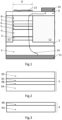
- FIG.1 presents schematically a vertical profile of a hybrid diode according to the invention
- Fig.2 presenting a tunnel junction structure of the diode from Fig.1
- Fig.3 presenting a hole injection layer structure of the same diode.
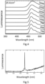
- Fig.4 presents a spectrum of electroluminescence of a source of light exciting the photon emitter from Fig.1 for eight different temperatures ranging from 10 K to 300 K.
- Fig.5 presents a spectrum of an excited photon emitter from Fig.1 at the temperature of 10 K
- Fig.6 presents a function of the g 2 correlation of the photons emitted by said emitter at the temperature of 10 K.
- the exciting light source of an embodiment of a hybrid diode according to the invention was fabricated in the process of nitrogen plasma-assisted molecular beam epitaxy (PAMBE) growth.
- the substrate 1 of gallium nitride with the thickness of 350 ⁇ m was baked in a prechamber at the temperature of 150°C for 1.5 hours. Subsequently, the baking was continued in a preparatory chamber at the temperature of 650°C for 30 minutes.
- the baked sample was transferred to a growth chamber and epitaxial growth was performed in metal-rich conditions.
- the nitrogen used for the growth was supplied in the form of plasma generated by a power supply unit with the power of 420 W and the nitrogen flow of 2 sccm.
- a lower n-type GaN conductivity layer 2 with the thickness of 75 nm and the silicon doping level of 5 ⁇ 10 19 cm -3 , was fabricated. Subsequently, the growth temperature was reduced to 650°C and a tunnel junction 3 with the thickness of 90 nm was fabricated.
- the tunnel junction 3 was composed of four sublayers: 3A, 3B, 3C and 3D ( Fig.2 ). The first, counted from the substrate 1, sublayer 3A with the thickness of 40 nm was made of a silicon-doped In 0.02 Ga 0.98 N alloy, with the doping level of 5 ⁇ 10 19 cm -3 .
- the second sublayer 3B with the thickness of 5 nm was made of a silicon-doped In 0.21 Ga 0.79 N alloy, with the doping level of 5 ⁇ 10 20 cm -3 .
- the third sublayer 3C with the thickness of 5 nm was made of a magnesium-doped In 0.21 Ga 0.79 N alloy, with the doping level of 5 ⁇ 10 20 cm -3 .
- the fourth sublayer 3D of the tunnel junction 3 had the thickness of 40 nm and was made of a magnesium-doped In 0.02 Ga 0.98 N alloy, with the doping level of 5 ⁇ 10 19 cm -3 .
- a hole injection layer 4 with the thickness of 125 nm was made of magnesium-doped GaN, with the first 100 nm of the thickness (4A) of the layer 4 was doped with magnesium with the doping level of 1 ⁇ 10 19 cm -3 , while the successive 25 nm of the thickness (4B) of the layer 4 was doped with magnesium with the doping level of 5 ⁇ 10 19 cm -3 ( Fig.3 ).
- the temperature was reduced to 650°C and an active region was fabricated, composed of a lower barrier layer 5 with the thickness of 30 nm, made of an undoped In 0.08 Ga 0.92 N alloy, of a quantum well layer 6 with the thickness of 15 nm, made of an undoped In 0.17 Ga 0.83 N alloy, and of an upper barrier layer 7 with the thickness of 30 nm made of an undoped In 0.08 Ga 0.92 N alloy.
- the temperature was increased and an electron injection layer 8 with the thickness of 150 nm was fabricated of GaN.
- the sample was removed from the molecular beam epitaxy (MBE) machine and subjected to the photolithography process for the purpose of creating target regions of emission of light that excites the emission of single photons.
- the sample was subjected to the process of He + implantation with the energy of 100 keV and the dose of 1.5 ⁇ 10 14 cm -3 . It is important that the implantation depth 12 is so deep enough for ions to penetrate the strongly doped tunnel junction 3.
- the sample was placed in the prechamber of the MBE machine at the temperature of 150°C for 1.5 hours. Subsequently, the baking was continued in a preparatory chamber at the temperature of 650°C for 30 minutes. The baked sample was transferred to a growth chamber and epitaxial growth of the upper n-type conductivity layer 9 with the thickness of 200 nm, made of silicon-doped GaN with the doping level of 8 ⁇ 10 18 cm -3 , was performed in metal-rich conditions.
- metallisation 10 (upper contact) with the thickness of 25 nm/75 nm was made on the gallium side outside the light emitting region and metallisation 11 (lower contact) was made on the whole nitrogen surface of the substrate 1.
- devices with contacts 10 and 11 with the dimensions of 350 ⁇ m x 350 ⁇ m were separated.
- the surface areas of the light emitting regions, limited by the regions 12, which were made electrically inactive as a result of ion implantation, ranged from 7 to 5000 ⁇ m 2 , arising from the diameters D of photoresist mask, with which the layer structure was shielded from the impact of the aforementioned ion implantation.
- the target light emitting region can be inscribed into a circle with the diameter D of at least 3 ⁇ m.
- a photon emitter 13 in the form of a WSe 2 monolayer was placed on the aforementioned light emitting region with the use of a micromanipulator. After applying the monolayer 13, the instrument was fastened in a TO5.6 type semiconductor package. Because the upper surface of the layer 9 is flat regardless of the LED light emitting region size, it is possible to place the emitter 13 layer thereon accurately.
- a tungsten disulfide (WS 2 ) monolayer or a molybdenum disulfide (MoS 2 ) monolayer can be used as an emitter 13 of a hybrid diode according to the invention.
- Fig.1 presents the current flow 14 from the lower 11 to the upper 10 contact by means of a dashed line.
- a high-conductive n-type layer (9) makes it possible to place an upper contact 10 outside the light emitting region with the diameter D.
- Fig.4 presents an electroluminescence spectrum of said diode for the current density of 25A/cm 2 for eight different operating temperatures ranging from 10 K to 300 K. Individual spectra are shifted along the vertical axis in the diagram to separate them for the purpose of a better presentation of the results. As shown by said diagram, the amplitude of the electroluminescence exciting the emitter 13 does not decrease in line with the reduction of the operating temperature, which makes it possible to effectively excite the TMD layer.
- the diagram shown in Fig.5 presents a spectrum of excitation of a WSe 2 monolayer to emit photons by the aforementioned LED operating at the temperature of 10 K. This diagram shows a very narrow emission line in the wavelength of 715.7 nm.
- Fig.6 presents the correlation function (g 2 ) of photons at the temperature of 10 K emitted by the aforementioned hybrid diode according to the invention for the aforementioned wavelength of 715.7 nm.
- the minimum of the function is only 0.22, while in the known devices for single photon emission a minimum of 0.5 is acceptable.
- the behaviour of the g 2 correlation function was determined in the Hanbury Brown and Twiss interferometer, wherein detailed information about the methods of quality assessment of devices that emit single photons, a description of the g 2 correlation function used for this purpose, and a description of the interferometer used in this embodiment are disclosed in the publication by Y. Arakawa, and M. Holmes, titled “Progress in quantum-dot single photon sources for quantum information technologies: A broad spectrum overview", [Appl. Phys. Rev. 7, 021309 (2020 )].
- the aforementioned hybrid diode according to the invention can operate within atemperature range from 1 to 300 K, with the optimum temperature range of operation being from 1 to 150 K.
Landscapes
- Physics & Mathematics (AREA)
- General Physics & Mathematics (AREA)
- Engineering & Computer Science (AREA)
- Theoretical Computer Science (AREA)
- Led Devices (AREA)
- Semiconductor Lasers (AREA)
Claims (6)
- Eine hybride Leuchtdiode zur Emission von Einzelphotonen, dadurch gekennzeichnet, dass sie einen Photonenemitter (13) in Form einer ÜbergangsmetallDichalcogenid (TMD)-Monoschicht und eine den Emitter (13) anregende Lichtquelle in Form einer epitaktischen Schichtstruktur einer Leuchtdiode aus Nitriden der Gruppe II auf einem kristallinen Substrat (1) aus Galliumnitrid enthält, wobei die Struktur, ausgehend von dem kristallinen Substrat (1), aus einer unteren n-Typ-Leitfähigkeitsschicht (2), einem Tunnelübergang (3), einer Lochinjektionsschicht (4), einem aktiven Bereich (5, 6, 7), einer Elektroneninjektionsschicht (8) und einer oberen n-Typ-Leitfähigkeitsschicht (9) besteht, wobei der Photonenemitter (13) auf der oberen Fläche der oberen n-Typ-Leitfähigkeitsschicht (9) angeordnet ist, in einem lichtemittierenden Bereich, der von einem Bereich (12) einer epitaktischen Struktur umgeben ist, die durch das Ionenimplantationsverfahren elektrisch inaktiv gemacht wurde, und der sich vertikal von der oberen Oberfläche der Elektroneninjektionsschicht (8) zur Innenseite der unteren n-Typ-Leitfähigkeitsschicht (2) erstreckt, die Oberfläche des lichtemittierenden Bereichs auf der oberen Oberfläche der Elektroneninjektionsschicht (8) liegt im Bereich von 7 bis 5000 µm2 und kann in einen Kreis mit dem Durchmesser (D) von mindestens 3 µm eingeschrieben werden, während der aktive Bereich der Leuchtdiode, von einem kristallinen Substrat (1) ausgehend, aus einer unteren Barriereschicht (5), einer Quantentopfschicht (6) und einer oberen Barriereschicht (7) besteht, wobei die untere (5) und die obere (7) Barriereschicht aus einer undotierten InxGa1-xN-Indium-GalliumNitrid-Legierung hergestellt sind, wobei der Indiumgehalt x im Bereich von 0,01 bis 0,08 liegt, während die Quantentopfschicht (6) aus einer undotierten InyGa1-yN-Indium-Gallium-Nitrid-Legierung besteht, wobei der Indiumgehalt y zwischen 0,1 und 0,2 liegt.
- Die Hybriddiode nach Anspruch 1, wobei der Photonenemitter (13) aus einer Wolframdiselenid (WSe2)-Monoschicht, aus einer Wolframdisulfid (WS2)-Monoschicht oder aus einer Molybdändisulfid (M0S2)-Monoschicht aufgebaut ist.
- Die Hybriddiode nach Anspruch 1 oder 2, wobei der Tunnelübergang (3) ausgehend von dem kristallinen Substrat (1) aus einer ersten Teilschicht (3A), einer zweiten Teilschicht (3B), einer dritten Teilschicht (3C) und einer vierten Teilschicht (3D) zusammengesetzt ist, die alle aus dotierten InyGa1-yN-Indium-Gallium-Nitrid-Legierungen bestehen, wobei die Indiumgehalte y in der ersten (3A) und in der vierten (3D) Teilschicht des Tunnelübergangs (3) identisch sind und zwischen 0,01 und 0,04 liegen und die Teilschichten (3A, 3D) mit Silizium (3A) bzw. Magnesium (3D) auf einem Niveau von 2 × 1019cm-3 to 5 × 1019 cm-3 dotiert sind, die Indiumgehalte y in der zweiten (3B) und in der dritten (3C) Teilschicht des Tunnelübergangs (3) identisch sind und zwischen 0,15 und 0,25 liegen, die zweite Teilschicht (3B) des Tunnelübergangs (3) ist mit Silizium oder Germanium dotiert, wobei das Dotierungsniveau zwischen 50 × 1019 cm-3 und 100 × 1019 cm-3 liegt, während die dritte Teilschicht (3C) des Tunnelübergangs (3) mit Magnesium dotiert ist, wobei das Dotierungsniveau zwischen 10×1019 cm-3 und 50 × 1019 cm-3 liegt.
- Ein Verfahren zur Herstellung einer hybriden lichtemittierenden Diode, die einzelne Photonen emittiert, enthaltend einen Photonenemitter in Form einer Übergangsmetalldichalcogenid (TMD)-Monoschicht und eine Lichtquelle, die den Photonenemitter anregt, wobei
zunächst eine epitaktische Schichtstruktur einer lichtemittierenden Diode, die die Rolle einer anregenden Lichtquelle erfüllt, durch Aufbringen von Schichten aus Nitriden der Gruppe II auf ein kristallines Substrat (1) aus Galliumnitrid im Verfahren der Stickstoff-Plasma-unterstützten Molekularstrahlepitaxie (PAMBE) hergestellt wird, wobei eine untere n-Typ-Leitfähigkeitsschicht (2), ein Tunnelübergang (3), eine Lochinjektionsschicht (4), ein aktiver Bereich (5, 6, 7) und eine Elektroneninjektionsschicht (8) nacheinander auf das vorgenannte Substrat (1) aufgebracht werden, anschließend der Schichtstruktur-Wachstumsprozess unterbrochen wird und das lichtemittierende Feld auf der oberen Oberfläche der Elektroneninjektionsschicht (8) begrenzt wird, indem das ursprüngliche lichtemittierende Feld mit einem epitaktischen Strukturbereich (12) umgeben wird, der durch das Ionenimplantationsverfahren elektrisch inaktiv gemacht wird und sich vertikal von der oberen Oberfläche der Elektroneninjektionsschicht (8) zur Innenseite der unteren n-Typ-Leitfähigkeitsschicht (2) erstreckt, so dass die Oberfläche des begrenzten Lichtemissionsfeldes im Bereich von 7 bis 5000 µm2 liegt und in einen Kreis mit einem Durchmesser (D) von mindestens 3 µm eingeschrieben werden kann, nach der Begrenzung des Lichtemissionsfeldes wird das Wachstum der epitaktischen Struktur durch Aufbringen einer oberen n-Typ-Leitfähigkeitsschicht (9) beendet, und anschließend wird ein Photonenemitter (13) auf der oberen Oberfläche der hergestellten oberen n-Typ-Leitfähigkeitsschicht (9) angeordnet, in dem zuvor begrenzten lichtemittierenden Feld angeordnet wird, während im Laufe der Herstellung des aktiven Bereichs einer lichtemittierenden Diode nacheinander eine untere Barriereschicht (5), eine Quantentopfschicht (6) und eine obere Barriereschicht (7), ausgehend von dem kristallinen Substrat (1), aufgebracht werden, wobei die untere (5) und die obere (7) Barriereschicht aus einer undotierten InxGa1-xN-Indium-Gallium-Nitrid-Legierung hergestellt sind, wobei der Indiumgehalt x im Bereich von 0,01 bis 0,08 liegt, während die Quantentopfschicht (6) aus einer undotierten InyGa1-yN-Indium-Gallium-Nitrid-Legierung hergestellt ist, wobei der Indiumgehalt y im Bereich von 0,1 bis 0,2 liegt. - Das Verfahren nach Anspruch 4, wobei eine Wolframdiselenid (WSe2)-Monoschicht, eine Wolframdisulfid (WS2)-Monoschicht oder eine Molybdändisulfid (M0S2)-Monoschicht als Photonenemitter (13) verwendet wird.
- Das Verfahren nach Anspruch 4 oder 5, wobei das Aufbringen des Tunnelübergangs (3) darin besteht, ausgehend von dem kristallinen Substrat (1) nacheinander eine erste Teilschicht (3A), eine zweite Teilschicht (3B), eine dritte Teilschicht (3C) und eine vierte Teilschicht (3D) aufzubringen, die aus dotierten InyGa1-yN-Indium-Gallium-Nitrid-Legierungen bestehen, dadurch gekennzeichnet, dass der Indiumgehalt y in der ersten (3A) und in der vierten (3D) Teilschicht des Tunnelübergangs (3) identisch ist und zwischen 0,01 bis 0,04 liegt und die Teilschichten (3A, 3D) mit Silizium (3A) bzw. Magnesium (3D) auf einem Niveau von 2×1019 cm-3 bis 5×1019cm-3 dotiert sind, die Indiumgehalte y in der zweiten (3B) und in der dritten (3C) Teilschicht des Tunnelübergangs (3) identisch sind und zwischen 0,15 und 0,25 liegen, die zweite Teilschicht (3B) des Tunnelübergangs (3) ist mit Silizium oder Germanium dotiert, wobei der Dotierungsgrad zwischen 50 × 1019 cm-3 und 100× 1019 cm-3 liegt, während die dritte Teilschicht (3C) des Tunnelübergangs (3) mit Magnesium dotiert ist, wobei der Dotierungsgrad zwischen 10 × 1019 cm-3 und 50 × 1019 cm-3 liegt.
Applications Claiming Priority (1)
| Application Number | Priority Date | Filing Date | Title |
|---|---|---|---|
| PL440480A PL440480A1 (pl) | 2022-02-26 | 2022-02-26 | Hybrydowa dioda elektroluminescencyjna emitująca pojedyncze fotony i sposób wytwarzania hybrydowej diody elektroluminescencyjnej emitującej pojedyncze fotony |
Publications (3)
| Publication Number | Publication Date |
|---|---|
| EP4239694A1 EP4239694A1 (de) | 2023-09-06 |
| EP4239694C0 EP4239694C0 (de) | 2024-09-25 |
| EP4239694B1 true EP4239694B1 (de) | 2024-09-25 |
Family
ID=85571287
Family Applications (1)
| Application Number | Title | Priority Date | Filing Date |
|---|---|---|---|
| EP23152548.6A Active EP4239694B1 (de) | 2022-02-26 | 2023-01-19 | Hybrid-leuchtdiode und verfahren zur herstellung davon |
Country Status (2)
| Country | Link |
|---|---|
| EP (1) | EP4239694B1 (de) |
| PL (2) | PL440480A1 (de) |
Families Citing this family (1)
| Publication number | Priority date | Publication date | Assignee | Title |
|---|---|---|---|---|
| CN120882185B (zh) * | 2025-09-26 | 2025-12-09 | 微玖(苏州)光电科技有限公司 | 一种基于隧道结的高性能红光Micro LED外延结构及制备方法 |
Family Cites Families (3)
| Publication number | Priority date | Publication date | Assignee | Title |
|---|---|---|---|---|
| DE102010014177A1 (de) * | 2010-04-01 | 2011-10-06 | Jenoptik Polymer Systems Gmbh | Oberflächenemittierende Halbleiter-Leuchtdiode |
| US10431956B2 (en) * | 2015-07-14 | 2019-10-01 | International Business Machines Corporation | Nanocavity monolayer laser monolithically integrated with LED pump |
| CN111261764B (zh) * | 2020-01-22 | 2021-10-15 | 山西穿越光电科技有限责任公司 | 一种蓝光/红光双色led芯片封装结构及制备方法 |
-
2022
- 2022-02-26 PL PL440480A patent/PL440480A1/pl unknown
-
2023
- 2023-01-19 EP EP23152548.6A patent/EP4239694B1/de active Active
- 2023-01-19 PL PL23152548.6T patent/PL4239694T3/pl unknown
Also Published As
| Publication number | Publication date |
|---|---|
| PL440480A1 (pl) | 2023-08-28 |
| EP4239694C0 (de) | 2024-09-25 |
| EP4239694A1 (de) | 2023-09-06 |
| PL4239694T3 (pl) | 2025-03-31 |
Similar Documents
| Publication | Publication Date | Title |
|---|---|---|
| US6139760A (en) | Short-wavelength optoelectronic device including field emission device and its fabricating method | |
| EP2504869B1 (de) | Led mit erhöhter injektionseffizienz | |
| US9583671B2 (en) | Quantum efficiency of multiple quantum wells | |
| TWI557937B (zh) | 具p型摻雜層之發光裝置 | |
| CN111095579B (zh) | 氮化物半导体发光元件和氮化物半导体发光元件的制造方法 | |
| US10685835B2 (en) | III-nitride tunnel junction with modified P-N interface | |
| CN113826220B (zh) | 光电器件 | |
| JP4833930B2 (ja) | 窒化物半導体を加工してなる発光デバイスの処理方法 | |
| KR102190859B1 (ko) | 발광 디바이스를 위한 p형 층을 형성하는 방법 | |
| EP4239694B1 (de) | Hybrid-leuchtdiode und verfahren zur herstellung davon | |
| EP3157068B1 (de) | Mehrschichtige halbleiterstruktur und verfahren zur herstellung davon | |
| EP4193391A1 (de) | Led-vorrichtung und verfahren zur herstellung einer led-vorrichtung | |
| US11177414B2 (en) | Optoelectronic component and method for producing an optoelectronic component | |
| WO2021087274A1 (en) | Method to improve the performance of gallium-containing light-emitting devices | |
| US20250015561A1 (en) | Method for producing a multiplicity of vertically emitting semiconductor laser diodes and vertically emitting semiconductor laser diode | |
| JP2011113877A (ja) | 光電気混載基板および半導体装置 | |
| US20070034858A1 (en) | Light-emitting diodes with quantum dots | |
| JP3630881B2 (ja) | 3族窒化物半導体発光素子の製造方法 | |
| KR101067296B1 (ko) | 질화물계 발광소자의 제조방법 | |
| CN115621390B (zh) | p-NiO为盖层的AlGaN紫外光发光二极管和激光器及其制备方法 | |
| US20250113664A1 (en) | Light-emitting devices excited by impact ionization | |
| JPH0669539A (ja) | 発光半導体装置およびその製造方法 | |
| He | Design, fabrication and optimization of III-nitride micro light emitting diodes for optical communication | |
| WO2024068284A1 (en) | Method for producing a semiconductor laser and semiconductor laser | |
| Tian | Novel micro-pixelated III-nitride light emitting diodes: fabrication, efficiency studies and applications |
Legal Events
| Date | Code | Title | Description |
|---|---|---|---|
| PUAI | Public reference made under article 153(3) epc to a published international application that has entered the european phase |
Free format text: ORIGINAL CODE: 0009012 |
|
| STAA | Information on the status of an ep patent application or granted ep patent |
Free format text: STATUS: THE APPLICATION HAS BEEN PUBLISHED |
|
| AK | Designated contracting states |
Kind code of ref document: A1 Designated state(s): AL AT BE BG CH CY CZ DE DK EE ES FI FR GB GR HR HU IE IS IT LI LT LU LV MC ME MK MT NL NO PL PT RO RS SE SI SK SM TR |
|
| STAA | Information on the status of an ep patent application or granted ep patent |
Free format text: STATUS: REQUEST FOR EXAMINATION WAS MADE |
|
| 17P | Request for examination filed |
Effective date: 20240305 |
|
| RBV | Designated contracting states (corrected) |
Designated state(s): AL AT BE BG CH CY CZ DE DK EE ES FI FR GB GR HR HU IE IS IT LI LT LU LV MC ME MK MT NL NO PL PT RO RS SE SI SK SM TR |
|
| GRAP | Despatch of communication of intention to grant a patent |
Free format text: ORIGINAL CODE: EPIDOSNIGR1 |
|
| STAA | Information on the status of an ep patent application or granted ep patent |
Free format text: STATUS: GRANT OF PATENT IS INTENDED |
|
| INTG | Intention to grant announced |
Effective date: 20240610 |
|
| GRAS | Grant fee paid |
Free format text: ORIGINAL CODE: EPIDOSNIGR3 |
|
| GRAA | (expected) grant |
Free format text: ORIGINAL CODE: 0009210 |
|
| STAA | Information on the status of an ep patent application or granted ep patent |
Free format text: STATUS: THE PATENT HAS BEEN GRANTED |
|
| AK | Designated contracting states |
Kind code of ref document: B1 Designated state(s): AL AT BE BG CH CY CZ DE DK EE ES FI FR GB GR HR HU IE IS IT LI LT LU LV MC ME MK MT NL NO PL PT RO RS SE SI SK SM TR |
|
| REG | Reference to a national code |
Ref country code: GB Ref legal event code: FG4D |
|
| REG | Reference to a national code |
Ref country code: CH Ref legal event code: EP |
|
| REG | Reference to a national code |
Ref country code: DE Ref legal event code: R096 Ref document number: 602023000602 Country of ref document: DE |
|
| REG | Reference to a national code |
Ref country code: IE Ref legal event code: FG4D |
|
| U01 | Request for unitary effect filed |
Effective date: 20241015 |
|
| U07 | Unitary effect registered |
Designated state(s): AT BE BG DE DK EE FI FR IT LT LU LV MT NL PT RO SE SI Effective date: 20241031 |
|
| PG25 | Lapsed in a contracting state [announced via postgrant information from national office to epo] |
Ref country code: NO Free format text: LAPSE BECAUSE OF FAILURE TO SUBMIT A TRANSLATION OF THE DESCRIPTION OR TO PAY THE FEE WITHIN THE PRESCRIBED TIME-LIMIT Effective date: 20241225 |
|
| PG25 | Lapsed in a contracting state [announced via postgrant information from national office to epo] |
Ref country code: GR Free format text: LAPSE BECAUSE OF FAILURE TO SUBMIT A TRANSLATION OF THE DESCRIPTION OR TO PAY THE FEE WITHIN THE PRESCRIBED TIME-LIMIT Effective date: 20241226 |
|
| PG25 | Lapsed in a contracting state [announced via postgrant information from national office to epo] |
Ref country code: RS Free format text: LAPSE BECAUSE OF FAILURE TO SUBMIT A TRANSLATION OF THE DESCRIPTION OR TO PAY THE FEE WITHIN THE PRESCRIBED TIME-LIMIT Effective date: 20241225 |
|
| PG25 | Lapsed in a contracting state [announced via postgrant information from national office to epo] |
Ref country code: RS Free format text: LAPSE BECAUSE OF FAILURE TO SUBMIT A TRANSLATION OF THE DESCRIPTION OR TO PAY THE FEE WITHIN THE PRESCRIBED TIME-LIMIT Effective date: 20241225 Ref country code: NO Free format text: LAPSE BECAUSE OF FAILURE TO SUBMIT A TRANSLATION OF THE DESCRIPTION OR TO PAY THE FEE WITHIN THE PRESCRIBED TIME-LIMIT Effective date: 20241225 Ref country code: GR Free format text: LAPSE BECAUSE OF FAILURE TO SUBMIT A TRANSLATION OF THE DESCRIPTION OR TO PAY THE FEE WITHIN THE PRESCRIBED TIME-LIMIT Effective date: 20241226 |
|
| U20 | Renewal fee for the european patent with unitary effect paid |
Year of fee payment: 3 Effective date: 20250127 |
|
| PG25 | Lapsed in a contracting state [announced via postgrant information from national office to epo] |
Ref country code: IS Free format text: LAPSE BECAUSE OF FAILURE TO SUBMIT A TRANSLATION OF THE DESCRIPTION OR TO PAY THE FEE WITHIN THE PRESCRIBED TIME-LIMIT Effective date: 20250125 |
|
| PG25 | Lapsed in a contracting state [announced via postgrant information from national office to epo] |
Ref country code: SM Free format text: LAPSE BECAUSE OF FAILURE TO SUBMIT A TRANSLATION OF THE DESCRIPTION OR TO PAY THE FEE WITHIN THE PRESCRIBED TIME-LIMIT Effective date: 20240925 |
|
| PG25 | Lapsed in a contracting state [announced via postgrant information from national office to epo] |
Ref country code: ES Free format text: LAPSE BECAUSE OF FAILURE TO SUBMIT A TRANSLATION OF THE DESCRIPTION OR TO PAY THE FEE WITHIN THE PRESCRIBED TIME-LIMIT Effective date: 20240925 |
|
| PG25 | Lapsed in a contracting state [announced via postgrant information from national office to epo] |
Ref country code: CZ Free format text: LAPSE BECAUSE OF FAILURE TO SUBMIT A TRANSLATION OF THE DESCRIPTION OR TO PAY THE FEE WITHIN THE PRESCRIBED TIME-LIMIT Effective date: 20240925 |
|
| PGFP | Annual fee paid to national office [announced via postgrant information from national office to epo] |
Ref country code: PL Payment date: 20250110 Year of fee payment: 3 |
|
| PG25 | Lapsed in a contracting state [announced via postgrant information from national office to epo] |
Ref country code: SK Free format text: LAPSE BECAUSE OF FAILURE TO SUBMIT A TRANSLATION OF THE DESCRIPTION OR TO PAY THE FEE WITHIN THE PRESCRIBED TIME-LIMIT Effective date: 20240925 |
|
| PLBE | No opposition filed within time limit |
Free format text: ORIGINAL CODE: 0009261 |
|
| STAA | Information on the status of an ep patent application or granted ep patent |
Free format text: STATUS: NO OPPOSITION FILED WITHIN TIME LIMIT |
|
| 26N | No opposition filed |
Effective date: 20250626 |
|
| PG25 | Lapsed in a contracting state [announced via postgrant information from national office to epo] |
Ref country code: MC Free format text: LAPSE BECAUSE OF FAILURE TO SUBMIT A TRANSLATION OF THE DESCRIPTION OR TO PAY THE FEE WITHIN THE PRESCRIBED TIME-LIMIT Effective date: 20240925 |