EP4239690A2 - Cellule solaire et méthode de fabrication - Google Patents
Cellule solaire et méthode de fabrication Download PDFInfo
- Publication number
- EP4239690A2 EP4239690A2 EP23186644.3A EP23186644A EP4239690A2 EP 4239690 A2 EP4239690 A2 EP 4239690A2 EP 23186644 A EP23186644 A EP 23186644A EP 4239690 A2 EP4239690 A2 EP 4239690A2
- Authority
- EP
- European Patent Office
- Prior art keywords
- passivation
- electrode region
- silicon substrate
- sublayer
- passivation structure
- Prior art date
- Legal status (The legal status is an assumption and is not a legal conclusion. Google has not performed a legal analysis and makes no representation as to the accuracy of the status listed.)
- Pending
Links
- 238000002360 preparation method Methods 0.000 title abstract description 5
- 238000002161 passivation Methods 0.000 claims abstract description 272
- XUIMIQQOPSSXEZ-UHFFFAOYSA-N Silicon Chemical compound [Si] XUIMIQQOPSSXEZ-UHFFFAOYSA-N 0.000 claims abstract description 117
- 229910052710 silicon Inorganic materials 0.000 claims abstract description 117
- 239000010703 silicon Substances 0.000 claims abstract description 117
- 239000000758 substrate Substances 0.000 claims abstract description 106
- 238000000034 method Methods 0.000 claims abstract description 68
- 229910021417 amorphous silicon Inorganic materials 0.000 claims description 42
- 230000005641 tunneling Effects 0.000 claims description 31
- 239000000463 material Substances 0.000 claims description 21
- 229910021420 polycrystalline silicon Inorganic materials 0.000 claims description 18
- VYPSYNLAJGMNEJ-UHFFFAOYSA-N Silicium dioxide Chemical compound O=[Si]=O VYPSYNLAJGMNEJ-UHFFFAOYSA-N 0.000 claims description 17
- 229920005591 polysilicon Polymers 0.000 claims description 17
- 238000000059 patterning Methods 0.000 claims description 15
- 229910052814 silicon oxide Inorganic materials 0.000 claims description 15
- HBMJWWWQQXIZIP-UHFFFAOYSA-N silicon carbide Chemical compound [Si+]#[C-] HBMJWWWQQXIZIP-UHFFFAOYSA-N 0.000 claims description 12
- 229910010271 silicon carbide Inorganic materials 0.000 claims description 12
- TWNQGVIAIRXVLR-UHFFFAOYSA-N oxo(oxoalumanyloxy)alumane Chemical compound O=[Al]O[Al]=O TWNQGVIAIRXVLR-UHFFFAOYSA-N 0.000 claims description 3
- 239000010410 layer Substances 0.000 description 69
- 238000011065 in-situ storage Methods 0.000 description 9
- 238000001039 wet etching Methods 0.000 description 9
- ZOXJGFHDIHLPTG-UHFFFAOYSA-N Boron Chemical compound [B] ZOXJGFHDIHLPTG-UHFFFAOYSA-N 0.000 description 7
- 238000009792 diffusion process Methods 0.000 description 7
- 238000000623 plasma-assisted chemical vapour deposition Methods 0.000 description 7
- OAICVXFJPJFONN-UHFFFAOYSA-N Phosphorus Chemical compound [P] OAICVXFJPJFONN-UHFFFAOYSA-N 0.000 description 6
- 230000015572 biosynthetic process Effects 0.000 description 6
- 229910052796 boron Inorganic materials 0.000 description 6
- 229910052698 phosphorus Inorganic materials 0.000 description 6
- 239000011574 phosphorus Substances 0.000 description 6
- 238000005240 physical vapour deposition Methods 0.000 description 5
- RYGMFSIKBFXOCR-UHFFFAOYSA-N Copper Chemical compound [Cu] RYGMFSIKBFXOCR-UHFFFAOYSA-N 0.000 description 4
- 238000000137 annealing Methods 0.000 description 4
- 229910052802 copper Inorganic materials 0.000 description 4
- 239000010949 copper Substances 0.000 description 4
- 238000004518 low pressure chemical vapour deposition Methods 0.000 description 4
- 230000003213 activating effect Effects 0.000 description 3
- QVGXLLKOCUKJST-UHFFFAOYSA-N atomic oxygen Chemical compound [O] QVGXLLKOCUKJST-UHFFFAOYSA-N 0.000 description 3
- 238000007641 inkjet printing Methods 0.000 description 3
- 238000010329 laser etching Methods 0.000 description 3
- 230000003287 optical effect Effects 0.000 description 3
- 229910052760 oxygen Inorganic materials 0.000 description 3
- 239000001301 oxygen Substances 0.000 description 3
- 239000002356 single layer Substances 0.000 description 3
- IJGRMHOSHXDMSA-UHFFFAOYSA-N Atomic nitrogen Chemical compound N#N IJGRMHOSHXDMSA-UHFFFAOYSA-N 0.000 description 2
- PXHVJJICTQNCMI-UHFFFAOYSA-N Nickel Chemical compound [Ni] PXHVJJICTQNCMI-UHFFFAOYSA-N 0.000 description 2
- 229910052581 Si3N4 Inorganic materials 0.000 description 2
- BQCADISMDOOEFD-UHFFFAOYSA-N Silver Chemical compound [Ag] BQCADISMDOOEFD-UHFFFAOYSA-N 0.000 description 2
- 238000010521 absorption reaction Methods 0.000 description 2
- 229910052782 aluminium Inorganic materials 0.000 description 2
- XAGFODPZIPBFFR-UHFFFAOYSA-N aluminium Chemical compound [Al] XAGFODPZIPBFFR-UHFFFAOYSA-N 0.000 description 2
- 238000006243 chemical reaction Methods 0.000 description 2
- 238000010586 diagram Methods 0.000 description 2
- 239000002019 doping agent Substances 0.000 description 2
- 238000005530 etching Methods 0.000 description 2
- 238000010438 heat treatment Methods 0.000 description 2
- 238000004050 hot filament vapor deposition Methods 0.000 description 2
- 238000011056 performance test Methods 0.000 description 2
- 238000001020 plasma etching Methods 0.000 description 2
- 239000011241 protective layer Substances 0.000 description 2
- 238000007650 screen-printing Methods 0.000 description 2
- 239000004065 semiconductor Substances 0.000 description 2
- HQVNEWCFYHHQES-UHFFFAOYSA-N silicon nitride Chemical compound N12[Si]34N5[Si]62N3[Si]51N64 HQVNEWCFYHHQES-UHFFFAOYSA-N 0.000 description 2
- 229910052709 silver Inorganic materials 0.000 description 2
- 239000004332 silver Substances 0.000 description 2
- 239000000126 substance Substances 0.000 description 2
- 239000002344 surface layer Substances 0.000 description 2
- ZXVONLUNISGICL-UHFFFAOYSA-N 4,6-dinitro-o-cresol Chemical compound CC1=CC([N+]([O-])=O)=CC([N+]([O-])=O)=C1O ZXVONLUNISGICL-UHFFFAOYSA-N 0.000 description 1
- 229910017107 AlOx Inorganic materials 0.000 description 1
- OKTJSMMVPCPJKN-UHFFFAOYSA-N Carbon Chemical compound [C] OKTJSMMVPCPJKN-UHFFFAOYSA-N 0.000 description 1
- GVGLGOZIDCSQPN-PVHGPHFFSA-N Heroin Chemical compound O([C@H]1[C@H](C=C[C@H]23)OC(C)=O)C4=C5[C@@]12CCN(C)[C@@H]3CC5=CC=C4OC(C)=O GVGLGOZIDCSQPN-PVHGPHFFSA-N 0.000 description 1
- 229910004012 SiCx Inorganic materials 0.000 description 1
- ATJFFYVFTNAWJD-UHFFFAOYSA-N Tin Chemical compound [Sn] ATJFFYVFTNAWJD-UHFFFAOYSA-N 0.000 description 1
- 229910052799 carbon Inorganic materials 0.000 description 1
- 238000005266 casting Methods 0.000 description 1
- 238000004140 cleaning Methods 0.000 description 1
- 238000004891 communication Methods 0.000 description 1
- 239000002131 composite material Substances 0.000 description 1
- 230000008094 contradictory effect Effects 0.000 description 1
- 238000000151 deposition Methods 0.000 description 1
- 230000008021 deposition Effects 0.000 description 1
- 239000003989 dielectric material Substances 0.000 description 1
- 238000009826 distribution Methods 0.000 description 1
- 238000009713 electroplating Methods 0.000 description 1
- 238000005247 gettering Methods 0.000 description 1
- 229910021478 group 5 element Inorganic materials 0.000 description 1
- BHEPBYXIRTUNPN-UHFFFAOYSA-N hydridophosphorus(.) (triplet) Chemical compound [PH] BHEPBYXIRTUNPN-UHFFFAOYSA-N 0.000 description 1
- 238000005224 laser annealing Methods 0.000 description 1
- 230000031700 light absorption Effects 0.000 description 1
- 239000007769 metal material Substances 0.000 description 1
- 229910021424 microcrystalline silicon Inorganic materials 0.000 description 1
- 238000012986 modification Methods 0.000 description 1
- 230000004048 modification Effects 0.000 description 1
- 229910021421 monocrystalline silicon Inorganic materials 0.000 description 1
- 229910021423 nanocrystalline silicon Inorganic materials 0.000 description 1
- 229910052759 nickel Inorganic materials 0.000 description 1
- 229910052757 nitrogen Inorganic materials 0.000 description 1
- 238000000206 photolithography Methods 0.000 description 1
- 238000005498 polishing Methods 0.000 description 1
- 239000002210 silicon-based material Substances 0.000 description 1
- 229910052718 tin Inorganic materials 0.000 description 1
- 238000007740 vapor deposition Methods 0.000 description 1
Images


Classifications
-
- H—ELECTRICITY
- H01—ELECTRIC ELEMENTS
- H01L—SEMICONDUCTOR DEVICES NOT COVERED BY CLASS H10
- H01L31/00—Semiconductor devices sensitive to infrared radiation, light, electromagnetic radiation of shorter wavelength or corpuscular radiation and specially adapted either for the conversion of the energy of such radiation into electrical energy or for the control of electrical energy by such radiation; Processes or apparatus specially adapted for the manufacture or treatment thereof or of parts thereof; Details thereof
- H01L31/02—Details
- H01L31/0216—Coatings
- H01L31/02161—Coatings for devices characterised by at least one potential jump barrier or surface barrier
- H01L31/02167—Coatings for devices characterised by at least one potential jump barrier or surface barrier for solar cells
-
- H—ELECTRICITY
- H01—ELECTRIC ELEMENTS
- H01L—SEMICONDUCTOR DEVICES NOT COVERED BY CLASS H10
- H01L31/00—Semiconductor devices sensitive to infrared radiation, light, electromagnetic radiation of shorter wavelength or corpuscular radiation and specially adapted either for the conversion of the energy of such radiation into electrical energy or for the control of electrical energy by such radiation; Processes or apparatus specially adapted for the manufacture or treatment thereof or of parts thereof; Details thereof
- H01L31/04—Semiconductor devices sensitive to infrared radiation, light, electromagnetic radiation of shorter wavelength or corpuscular radiation and specially adapted either for the conversion of the energy of such radiation into electrical energy or for the control of electrical energy by such radiation; Processes or apparatus specially adapted for the manufacture or treatment thereof or of parts thereof; Details thereof adapted as photovoltaic [PV] conversion devices
- H01L31/06—Semiconductor devices sensitive to infrared radiation, light, electromagnetic radiation of shorter wavelength or corpuscular radiation and specially adapted either for the conversion of the energy of such radiation into electrical energy or for the control of electrical energy by such radiation; Processes or apparatus specially adapted for the manufacture or treatment thereof or of parts thereof; Details thereof adapted as photovoltaic [PV] conversion devices characterised by at least one potential-jump barrier or surface barrier
- H01L31/072—Semiconductor devices sensitive to infrared radiation, light, electromagnetic radiation of shorter wavelength or corpuscular radiation and specially adapted either for the conversion of the energy of such radiation into electrical energy or for the control of electrical energy by such radiation; Processes or apparatus specially adapted for the manufacture or treatment thereof or of parts thereof; Details thereof adapted as photovoltaic [PV] conversion devices characterised by at least one potential-jump barrier or surface barrier the potential barriers being only of the PN heterojunction type
- H01L31/0745—Semiconductor devices sensitive to infrared radiation, light, electromagnetic radiation of shorter wavelength or corpuscular radiation and specially adapted either for the conversion of the energy of such radiation into electrical energy or for the control of electrical energy by such radiation; Processes or apparatus specially adapted for the manufacture or treatment thereof or of parts thereof; Details thereof adapted as photovoltaic [PV] conversion devices characterised by at least one potential-jump barrier or surface barrier the potential barriers being only of the PN heterojunction type comprising a AIVBIV heterojunction, e.g. Si/Ge, SiGe/Si or Si/SiC solar cells
- H01L31/0747—Semiconductor devices sensitive to infrared radiation, light, electromagnetic radiation of shorter wavelength or corpuscular radiation and specially adapted either for the conversion of the energy of such radiation into electrical energy or for the control of electrical energy by such radiation; Processes or apparatus specially adapted for the manufacture or treatment thereof or of parts thereof; Details thereof adapted as photovoltaic [PV] conversion devices characterised by at least one potential-jump barrier or surface barrier the potential barriers being only of the PN heterojunction type comprising a AIVBIV heterojunction, e.g. Si/Ge, SiGe/Si or Si/SiC solar cells comprising a heterojunction of crystalline and amorphous materials, e.g. heterojunction with intrinsic thin layer or HIT® solar cells; solar cells
-
- H—ELECTRICITY
- H01—ELECTRIC ELEMENTS
- H01L—SEMICONDUCTOR DEVICES NOT COVERED BY CLASS H10
- H01L31/00—Semiconductor devices sensitive to infrared radiation, light, electromagnetic radiation of shorter wavelength or corpuscular radiation and specially adapted either for the conversion of the energy of such radiation into electrical energy or for the control of electrical energy by such radiation; Processes or apparatus specially adapted for the manufacture or treatment thereof or of parts thereof; Details thereof
- H01L31/02—Details
- H01L31/0224—Electrodes
- H01L31/022408—Electrodes for devices characterised by at least one potential jump barrier or surface barrier
- H01L31/022425—Electrodes for devices characterised by at least one potential jump barrier or surface barrier for solar cells
- H01L31/022441—Electrode arrangements specially adapted for back-contact solar cells
-
- H—ELECTRICITY
- H01—ELECTRIC ELEMENTS
- H01L—SEMICONDUCTOR DEVICES NOT COVERED BY CLASS H10
- H01L31/00—Semiconductor devices sensitive to infrared radiation, light, electromagnetic radiation of shorter wavelength or corpuscular radiation and specially adapted either for the conversion of the energy of such radiation into electrical energy or for the control of electrical energy by such radiation; Processes or apparatus specially adapted for the manufacture or treatment thereof or of parts thereof; Details thereof
- H01L31/04—Semiconductor devices sensitive to infrared radiation, light, electromagnetic radiation of shorter wavelength or corpuscular radiation and specially adapted either for the conversion of the energy of such radiation into electrical energy or for the control of electrical energy by such radiation; Processes or apparatus specially adapted for the manufacture or treatment thereof or of parts thereof; Details thereof adapted as photovoltaic [PV] conversion devices
- H01L31/06—Semiconductor devices sensitive to infrared radiation, light, electromagnetic radiation of shorter wavelength or corpuscular radiation and specially adapted either for the conversion of the energy of such radiation into electrical energy or for the control of electrical energy by such radiation; Processes or apparatus specially adapted for the manufacture or treatment thereof or of parts thereof; Details thereof adapted as photovoltaic [PV] conversion devices characterised by at least one potential-jump barrier or surface barrier
- H01L31/068—Semiconductor devices sensitive to infrared radiation, light, electromagnetic radiation of shorter wavelength or corpuscular radiation and specially adapted either for the conversion of the energy of such radiation into electrical energy or for the control of electrical energy by such radiation; Processes or apparatus specially adapted for the manufacture or treatment thereof or of parts thereof; Details thereof adapted as photovoltaic [PV] conversion devices characterised by at least one potential-jump barrier or surface barrier the potential barriers being only of the PN homojunction type, e.g. bulk silicon PN homojunction solar cells or thin film polycrystalline silicon PN homojunction solar cells
- H01L31/0682—Semiconductor devices sensitive to infrared radiation, light, electromagnetic radiation of shorter wavelength or corpuscular radiation and specially adapted either for the conversion of the energy of such radiation into electrical energy or for the control of electrical energy by such radiation; Processes or apparatus specially adapted for the manufacture or treatment thereof or of parts thereof; Details thereof adapted as photovoltaic [PV] conversion devices characterised by at least one potential-jump barrier or surface barrier the potential barriers being only of the PN homojunction type, e.g. bulk silicon PN homojunction solar cells or thin film polycrystalline silicon PN homojunction solar cells back-junction, i.e. rearside emitter, solar cells, e.g. interdigitated base-emitter regions back-junction cells
-
- H—ELECTRICITY
- H01—ELECTRIC ELEMENTS
- H01L—SEMICONDUCTOR DEVICES NOT COVERED BY CLASS H10
- H01L31/00—Semiconductor devices sensitive to infrared radiation, light, electromagnetic radiation of shorter wavelength or corpuscular radiation and specially adapted either for the conversion of the energy of such radiation into electrical energy or for the control of electrical energy by such radiation; Processes or apparatus specially adapted for the manufacture or treatment thereof or of parts thereof; Details thereof
- H01L31/04—Semiconductor devices sensitive to infrared radiation, light, electromagnetic radiation of shorter wavelength or corpuscular radiation and specially adapted either for the conversion of the energy of such radiation into electrical energy or for the control of electrical energy by such radiation; Processes or apparatus specially adapted for the manufacture or treatment thereof or of parts thereof; Details thereof adapted as photovoltaic [PV] conversion devices
- H01L31/06—Semiconductor devices sensitive to infrared radiation, light, electromagnetic radiation of shorter wavelength or corpuscular radiation and specially adapted either for the conversion of the energy of such radiation into electrical energy or for the control of electrical energy by such radiation; Processes or apparatus specially adapted for the manufacture or treatment thereof or of parts thereof; Details thereof adapted as photovoltaic [PV] conversion devices characterised by at least one potential-jump barrier or surface barrier
- H01L31/072—Semiconductor devices sensitive to infrared radiation, light, electromagnetic radiation of shorter wavelength or corpuscular radiation and specially adapted either for the conversion of the energy of such radiation into electrical energy or for the control of electrical energy by such radiation; Processes or apparatus specially adapted for the manufacture or treatment thereof or of parts thereof; Details thereof adapted as photovoltaic [PV] conversion devices characterised by at least one potential-jump barrier or surface barrier the potential barriers being only of the PN heterojunction type
- H01L31/0745—Semiconductor devices sensitive to infrared radiation, light, electromagnetic radiation of shorter wavelength or corpuscular radiation and specially adapted either for the conversion of the energy of such radiation into electrical energy or for the control of electrical energy by such radiation; Processes or apparatus specially adapted for the manufacture or treatment thereof or of parts thereof; Details thereof adapted as photovoltaic [PV] conversion devices characterised by at least one potential-jump barrier or surface barrier the potential barriers being only of the PN heterojunction type comprising a AIVBIV heterojunction, e.g. Si/Ge, SiGe/Si or Si/SiC solar cells
-
- H—ELECTRICITY
- H01—ELECTRIC ELEMENTS
- H01L—SEMICONDUCTOR DEVICES NOT COVERED BY CLASS H10
- H01L31/00—Semiconductor devices sensitive to infrared radiation, light, electromagnetic radiation of shorter wavelength or corpuscular radiation and specially adapted either for the conversion of the energy of such radiation into electrical energy or for the control of electrical energy by such radiation; Processes or apparatus specially adapted for the manufacture or treatment thereof or of parts thereof; Details thereof
- H01L31/18—Processes or apparatus specially adapted for the manufacture or treatment of these devices or of parts thereof
- H01L31/1804—Processes or apparatus specially adapted for the manufacture or treatment of these devices or of parts thereof comprising only elements of Group IV of the Periodic System
-
- H—ELECTRICITY
- H01—ELECTRIC ELEMENTS
- H01L—SEMICONDUCTOR DEVICES NOT COVERED BY CLASS H10
- H01L31/00—Semiconductor devices sensitive to infrared radiation, light, electromagnetic radiation of shorter wavelength or corpuscular radiation and specially adapted either for the conversion of the energy of such radiation into electrical energy or for the control of electrical energy by such radiation; Processes or apparatus specially adapted for the manufacture or treatment thereof or of parts thereof; Details thereof
- H01L31/18—Processes or apparatus specially adapted for the manufacture or treatment of these devices or of parts thereof
- H01L31/186—Particular post-treatment for the devices, e.g. annealing, impurity gettering, short-circuit elimination, recrystallisation
- H01L31/1868—Passivation
-
- Y—GENERAL TAGGING OF NEW TECHNOLOGICAL DEVELOPMENTS; GENERAL TAGGING OF CROSS-SECTIONAL TECHNOLOGIES SPANNING OVER SEVERAL SECTIONS OF THE IPC; TECHNICAL SUBJECTS COVERED BY FORMER USPC CROSS-REFERENCE ART COLLECTIONS [XRACs] AND DIGESTS
- Y02—TECHNOLOGIES OR APPLICATIONS FOR MITIGATION OR ADAPTATION AGAINST CLIMATE CHANGE
- Y02P—CLIMATE CHANGE MITIGATION TECHNOLOGIES IN THE PRODUCTION OR PROCESSING OF GOODS
- Y02P70/00—Climate change mitigation technologies in the production process for final industrial or consumer products
- Y02P70/50—Manufacturing or production processes characterised by the final manufactured product
Definitions
- the present disclosure relates to the technical fields of solar cells, and in particular, to a solar cell and a preparation method thereof.
- an intrinsic a-Si layer is disposed on a back side (a side facing away from a light incident side) of a silicon substrate, while a base electrode and an emitter electrode are disposed on a side of the intrinsic a-Si layer away from the silicon substrate, and different polarities are doped on a surface of the intrinsic a-Si layer corresponding to different electrodes, respectively.
- HBC Heterojunction Back Contact
- the present disclosure provides a solar cell with a novel structure and a preparation method thereof.
- an embodiment of the present disclosure provides a solar cell, including:
- the second passivation structure is located in the second electrode region.
- the first passivation structure includes:
- the tunneling passivation sublayer is made of a material including at least one of silicon oxide, aluminum oxide, silicon oxynitride or silicon carbide; and the first passivation sublayer is made of a material including at least one of doped polysilicon or doped silicon carbide.
- the tunneling passivation sublayer has a thickness ranging from 1nm to 3nm; and the first passivation sublayer has a thickness ranging from 10nm to 200nm.
- the second passivation structure includes:
- the dielectric passivation sublayer is made of a material including at least one of polysilicon, amorphous silicon or silicon oxide; and the second passivation sublayer is made of a material including at least one of doped polysilicon, doped amorphous silicon or doped silicon carbide.
- the dielectric passivation sublayer has a thickness ranging from 1nm to 15nm; and the second passivation sublayer has a thickness ranging from 1nm to 20nm.
- the first electrode region includes a plurality of strip-shaped regions spaced apart
- the second electrode region includes a plurality of strip-shaped regions spaced apart
- the strip-shaped regions in the first electrode region and the strip-shaped regions in the second electrode region are alternately distributed.
- the first passivation structure has a process temperature ranging from 300 °C to 650 °C; and the second passivation structure has a process temperature ranging from 150 °C to 200 °C.
- an embodiment of the present disclosure provides a method for preparing a solar cell, wherein the solar cell is a solar cell according to any embodiment of the present disclosure, and the method includes:
- both electrodes are disposed on the back side of the silicon substrate, and passivation layers (the first passivation structure and the second passivation structure) with different polarities are disposed on the silicon substrate at positions corresponding to the two electrodes, respectively, so that a novel form of hybrid HBC solar cell is provided.
- first polarity and second polarity refer to two semiconductor types; that is, the first polarity and the second polarity are P-type (transporting holes) and N-type (transporting electrons) respectively and non-repetitively.
- first polarity may be P-type and the second polarity may be the N-type, or the first polarity may be the N-type and the second polarity may be P-type.
- the phrase "A is on a side of B away from C" means that A and B are both formed on a same side of C, and A is formed after B, so that A covers B at a position with both A and B.
- process temperature of a structure refers to the maximum temperature to be reached in formation of the structure.
- patterning process refers to a process for forming a structure having a specific pattern, which may specifically include a photolithography process, a laser process, a wet film etching process, or the like.
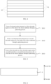
- a Heterojunction Back Contact (HBC) solar cell includes a silicon substrate 9.
- An intrinsic a-Si layer 59 is disposed on a back side (a first side) of the silicon substrate 9, while N-type doped regions 51 and P-type doped regions 52 are alternately formed on a surface of the intrinsic a-Si layer 59 to transport holes and electrons, respectively, and different types of electrodes, i.e., a first electrode 81 (e.g., a base electrode) and a second electrode 82 (e.g., an emitter electrode) arranged in an interdigitated manner are disposed on a side of the two types of doped regions away from the silicon substrate 9.
- a first electrode 81 e.g., a base electrode
- a second electrode 82 e.g., an emitter electrode
- a front dielectric passivation layer 31, an antireflection layer 32, and other structures may be further disposed sequentially on a light incident side (a second side) of the silicon substrate 9.
- the PN junction, and also the base electrode and the emitter electrode are all located on the back side so that no electrode is provided on the light incident side of the HBC solar cell, and thus light will not be shielded by electrodes. Therefore, the HBC solar cell has smaller optical loss, higher short-circuit current density, higher efficiency and better performance.
- an embodiment of the present disclosure provides a solar cell, including:
- the solar cell according to the embodiment of the present disclosure has a silicon substrate 9 with a certain polarity (a first polarity or a second polarity), which is a P-type doped or N-type doped silicon-based semiconductor.
- the silicon substrate 9 has a first side and a second side opposite to each other.
- the second side may be a "light incident side” for light incidence
- the first side may be a "back side” opposite to the light incident side.
- one part of a surface on the first side of the silicon substrate 9 is a first electrode region 91 for disposing the first electrode 81, and the other part is a second electrode region 92 for disposing the second electrode 82.
- first electrode region 91 and the second electrode region 92 are different regions, i.e., may be non-overlapping; and further, the first electrode region 91 and the second electrode region 92 may "completely cover" the first side of the silicon substrate 9.
- first electrode region 91 and the second electrode region 92 do not completely cover the first side of the silicon sub strate 9.
- the first electrode region 91 includes a plurality of strip-shaped regions spaced apart
- the second electrode region 92 includes a plurality of strip-shaped regions spaced apart
- the strip-shaped regions of the first electrode region 91 and the strip-shaped regions of the second electrode region 92 are alternately distributed.
- the first electrode region 91 may include a plurality of strips parallel to and spaced apart from each other
- the second electrode region 92 may also include a plurality of strips parallel to and spaced apart from each other
- the strips of the two electrode regions are parallel to each other and alternately distributed along a width direction of the stripes (apparently, the stripes of the two electrode regions may contact each other on sides, as shown in FIG. 4 , or may be spaced apart from each other by a certain distance).
- the first electrode 81 and the second electrode 82 in the first electrode region 91 and the second electrode region 92, respectively, are distributed in an "interdigitated" manner.
- a first passivation structure 1 (passivation layer) in the first electrode region 91 is disposed on the first side of the silicon substrate 9.
- the first passivation structure 1 is "patterned", and a position where the first passivation structure 1 is located is the first electrode region 91 (therefore, the first passivation structure 1 completely covers, but does not exceed, the first electrode region 91).
- the first passivation structure 1 has a polarity (first polarity), which is the same as or opposite to the polarity of the silicon substrate 9, in at least a surface layer farthest from the silicon substrate 9.
- a second passivation structure 2 is further disposed on a side of the first passivation structure 1 away from the silicon substrate 9 and in the second electrode region 92.
- the second passivation structure 2 is also "patterned", and a position where the second passivation structure 2 is located is the second electrode region 92(therefore, the second passivation structure 2 completely covers, but does not exceed, the second electrode region 92).
- first passivation structure 1 and the first passivation structure 2 are located at different electrode regions, there is no overlap therebetween. For example, if the first electrode region 91 and the second electrode region 92 "completely cover" the first side of the silicon substrate 9, since the first passivation structure 1 and the second passivation structure 2 fill the first electrode region 91 and the second electrode region 92, respectively, referring to FIG. 2 , the two passivation structures may contact each other on sides.
- the second passivation structure 2 has a polarity (second polarity), which is "opposite" to that of the first passivation structure 1, in at least a surface layer farthest from the silicon substrate 9.
- second polarity second polarity
- the first passivation structure 1 is P-type
- the second passivation structure 2 is the N-type
- the first passivation structure 1 is the N-type
- the second passivation structure 2 is P-type. Therefore, one of the first passivation structure 1 and the second passivation structure 2 has the same polarity as the silicon substrate 9, while the other has an opposite polarity to the silicon sub strate 9.
- the first passivation structure 1 and the second passivation structure 2 are disposed in the first electrode region 91 and the second electrode region 92, respectively, on the first side of the silicon substrate 9, and the first electrode 81 and the second electrode 82 are disposed on the first passivation structure 1 and the second passivation structure 2, respectively.
- the first passivation structure 1 and the second passivation structure 2 have opposite polarities, one has the same polarity as the silicon substrate 9, and the other has an opposite polarity to the silicon substrate 9.
- one of the first passivation structure 1 and the second passivation structure 2 may form a tunneling junction on the back side of the silicon substrate 9.
- the first passivation structure 1 and the second passivation structure 2 are distinguished through a comparison of their respective process temperatures. That is, the second passivation structure 2 has a lower process temperature than the first passivation structure 1. Therefore, the first passivation structure 1 is a high-temperature passivation structure (high-temperature passivation layer) having a higher process temperature, while the second passivation structure 2 is a low-temperature passivation structure (low-temperature passivation layer) having a lower process temperature.
- an order of formation of the second passivation structure 2 and the first passivation structure 1 may be determined from the structure of the solar cell product. If the first passivation structure 1 is formed first, heating in subsequent formation of the second passivation structure 2 will not affect the already formed first passivation structure 1; but if the second passivation structure 2 is formed first, heating in subsequent formation of the first passivation structure 1 may damage the already formed second passivation structure 2.
- the first passivation structure 1 has a process temperature ranging from 300 °C to 650 °C; and the second passivation structure 2 has a process temperature ranging from 150 °C to 200 °C.
- a maximum temperature (process temperature) in formation of the first passivation structure 1 may be 300 °C to 650 °C, or further 400°C to 600 °C. Accordingly, a maximum temperature (process temperature) in formation of the second passivation structure 2 may be 150 °C to 200 °C, or further 170°C to 190 °C.
- a first electrode 81 that does "not exceed” the first electrode region 91 is disposed on a side of the second passivation structure 2 away from the silicon substrate 9. In other words, the first electrode 81 is in communication with the silicon substrate 9 through the first passivation structure 1. Further, a second electrode 82 that does "not exceed” the second electrode region 92 is disposed on a side of the second passivation structure 2 away from the silicon substrate 9. In other words, the second electrode 82 is in conduction with the silicon substrate 9 through the second passivation structure 2.
- One of the first electrode 81 and the second electrode 82 is an emitter electrode, and the other is a base electrode.
- an electrode on the passivation structure having the same polarity as the substrate 9 is the base electrode, and an electrode on the passivation structure having the opposite polarity to the substrate 9 is the emitter electrode.
- both electrodes are disposed on the back side of the silicon substrate 9, and passivation layers (the first passivation structure 1 and the second passivation structure 2) with different polarities are disposed on the silicon substrate 9 at positions corresponding to the two electrodes, respectively, so that a novel form of hybrid HBC solar cell is provided.
- the first passivation structure 1 includes:
- the first passivation structure 1 may specifically include two sublayers, i.e., a tunneling passivation sublayer 11 contacting the silicon substrate 9, and a first passivation sublayer 12 on the tunneling passivation sublayer 11. At least the first passivation sublayer 12 has a first polarity opposite to the second passivation structure 2, e.g., a doped P-type or N-type.
- tunneling passivation sublayer 11 and the first passivation sublayer 12 are both patterned and have a same pattern.
- the tunneling passivation sublayer 11 is made of a material including at least one of silicon oxide, aluminum oxide, silicon oxynitride or silicon carbide; and the first passivation sublayer 12 is made of a material including at least one of doped polysilicon or doped silicon carbide.
- the tunneling passivation sublayer 11 may be made of a material selected from SiOx, AlOx, SiNOx, SiCx, or any other dielectric material.
- the tunneling passivation sublayer 11 may be free-dopant and thus may have no polarity.
- the first passivation sublayer 12 in the first passivation structure 1 has a first polarity opposite to the second passivation structure 2, which may be specifically a P-type or N-type doped polysilicon, silicon carbide or the like.
- the first passivation sublayer 12 may be doped with a group III element, such as boron (B); if the first polarity is N-type, the first passivation sublayer 12 may be doped with a V group element, such as phosphorus (P).
- group III element such as boron (B)
- V group element such as phosphorus (P).
- optical absorption can be further reduced, while effective doping of a higher concentration can be implemented, thereby reducing the contact resistance of the electrode and improving the cell fill factor.
- the tunneling passivation sublayer 11 has a thickness ranging from 1nm to 3nm; and the first passivation sublayer 12 has a thickness ranging from 10nm to 200nm.
- the tunneling passivation sublayer 11 in the first passivation structure 1 may have a thickness (a dimension in a direction perpendicular to the first side of the silicon substrate 9) ranging from 1 to 3nm, and further from 1.5 to 2nm; and the first passivation sublayer 12 may have a thickness ranging from 10 to 200nm, and further from 80 to 120nm.
- the second passivation structure 2 includes:
- the second passivation structure 2 may also include two sublayers, i.e., a dielectric passivation sublayer 21 close to the silicon substrate 9, and a second passivation sublayer 22 on the dielectric passivation sublayer 21. At least the second passivation sublayer 22 has a second polarity opposite to the first passivation structure 1.
- dielectric passivation sublayer 21 and the second passivation sublayer 22 are both patterned and have a same pattern.
- the dielectric passivation sublayer 21 is made of a material including at least one of polysilicon, amorphous silicon or silicon oxide; and the second passivation sublayer 22 is made of a material including at least one of doped polysilicon, doped amorphous silicon or doped silicon carbide.
- the dielectric passivation sublayer 21 may be specifically made of a material including amorphous silicon, polysilicon (poly-Si, which may be specifically microcrystalline silicon, nanocrystalline silicon) or the like, and may be a single layer or a stacked structure of layers of various different materials.
- the dielectric passivation sublayer 21 may be non-polar, i.e., an intrinsic free-dopant layer.
- the second passivation sublayer 22 has an opposite polarity to the first passivation structure 1, and may be, for example, made of a material including doped polysilicon, amorphous silicon, silicon carbide, or the like, where the doped element may be a group III element (e.g., boron) or a group V element (e.g., phosphorus), or the like.
- group III element e.g., boron
- a group V element e.g., phosphorus
- the dielectric passivation sublayer 21 has a thickness ranging from 1nm to 15nm; and the second passivation sublayer 22 has a thickness ranging from 1nm to 20nm.
- the dielectric passivation sublayer 21 may have a thickness ranging from 1 to 15nm, and further from 5 to 8nm; and the second passivation sublayer 22 may have a thickness ranging from 1 to 20nm, and further from 5 to 15nm.
- the silicon substrate 9 may be in the form of monocrystalline silicon, polysilicon, or the like, and doped to produce a desired polarity.
- a textured surface may be formed on the second side (light incident side) of the silicon substrate 9 to increase absorption of light.
- a complete front dielectric passivation layer 31 which may be specifically made of the same material as the second passivation sublayer 22 in the second passivation structure 2, may be formed on the second side of the silicon substrate 9,
- an antireflection layer 32 may be further formed on the second side of the silicon substrate 9 (e.g., outside the front dielectric passivation layer 31) to reduce light emission.
- the antireflection layer 32 may also serve as a protective layer (AR film) that may be specifically made of a material including one or more of silicon oxide, silicon nitride, silicon oxynitride, or the like, and may be a single layer or a stacked structure of multiple layers with different refractive indexes.
- a transparent conductive oxide (TCO) layer 89 for improving the contact resistance may be further provided between the electrode and the second passivation structure 2.
- the TCO layer 89 may be, for example, a single layer of ITO, IWO, AZO, ICO, IMO, IHO, SCOT or the like, or a stacked structure of multiple layers of different materials.
- a gap may be provided between transparent conductive oxide layers 89 in different electrode regions.
- the first electrode 81 and the second electrode 82 may be disposed in a same layer (made simultaneously of a same material), and made of a metal material including silver, copper, aluminum, tin-clad copper, silver-clad copper, or may be composite electrodes made of various materials including nickel, copper, aluminum, tin or the like.
- an embodiment of the present disclosure provides a method for preparing a solar cell, where the solar cell is a solar cell according to any embodiment of the present disclosure.
- the method provided in the embodiment of the present disclosure is used for preparing the solar cell as described above.
- a method for preparing a solar cell according to an embodiment of the present disclosure includes the following steps S101 to S103.
- the first passivation structure 1 in the first electrode region 91 and the second passivation structure 2 in the second electrode region 92 may be sequentially formed on the first side of the silicon substrate 9 through a patterning process; and then the first electrode 81 and the second electrode 82 in the first electrode region 91 and the second electrode region 92 are formed, respectively.
- the silicon substrate 9 may be formed through a czochralski method (CZ), a float zone method (FZ), a casting method, or the like.
- CZ czochralski method
- FZ float zone method
- casting method or the like.
- the silicon substrate 9 may be cleaned and polished before being subjected to any other step.
- the texture may be formed through wet chemical texturing, dry reactive ion etching (RIE), or the like.
- the front dielectric passivation layer 31 as described above may be formed on the second side of the silicon substrate 9 through plasma enhanced chemical vapor deposition (PECVD), hot wire chemical vapor deposition (HWCVD), or the like.
- PECVD plasma enhanced chemical vapor deposition
- HWCVD hot wire chemical vapor deposition
- the antireflection layer 32 (protective layer) as described above may be further formed on the second side of the silicon substrate 9 through PECVD or the like.
- a complete first passivation structure 1 may be formed first, and then patterned to remove the first passivation structure 1 from the second electrode region 92.
- the complete first passivation structure 1 may be formed by any one of the following methods.
- a very thin PSG (silicon oxide containing phosphorus) or BSG (silicon oxide containing boron) structure is synchronously formed on the surface of the first passivation sublayer 12, and may be used as a mask in subsequent processes.
- ELA excimer laser annealing
- a proper amount of oxygen (O 2 ) may be simultaneously introduced so that a PSG (or BSG) structure is synchronously formed on the surface of the first passivation sublayer 12 and serves as a mask in subsequent processes.
- the silicon oxynitride layer does not belong to the first passivation structure 1, but serves as a mask in subsequent processes.
- the complete first passivation structure 1 when formed, may be patterned by any one of the following modes.
- Mode I when the first passivation structure 1 is formed by any one of the above methods (1) to (3), a mask of a PSG (or BSG) structure, a silicon oxynitride layer, or the like is provided, so the mask on the second electrode region 92 may be removed through laser film opening, and then the first passivation structure 1 is removed from the second electrode region 92 through wet etching, while the first passivation structure 1 in the first electrode region 91 is protected by the mask and not etched, thereby completing patterning of the first passivation structure 1. Thereafter, the mask on the first electrode region 91 is removed.
- a mask of a PSG (or BSG) structure, a silicon oxynitride layer, or the like is provided, so the mask on the second electrode region 92 may be removed through laser film opening, and then the first passivation structure 1 is removed from the second electrode region 92 through wet etching, while the first passivation structure 1 in the first electrode region 91 is protected by the mask and not etched,
- Mode II when the first passivation structure 1 is formed by the above method (4) and including no mask, ink may be formed on the first electrode region 91 through inkjet printing as a mask, and then the first passivation structure 1 is removed from the second electrode region 92 through wet etching. Thereafter, the ink mask on the first electrode region 91 is removed.
- first passivation structure 1 when the complete first passivation structure 1 is formed according to the above modes I and II, it is equivalent that a mask (for patterning the first passivation structure 1) is formed at the same time of preparing the first passivation structure 1, and thus, a separate step of preparing the mask is omitted, which simplifies the process, and can further reduce one process of preparing the mask (such as forming ink).
- the diffused element therein can further form a phosphorus or boron diffusion layer on the second side of the silicon substrate 9 synchronously, which plays a role of phosphorus or boron gettering. Further, the diffusion layer can be naturally removed during the subsequent patterning (wet etching) of the first passivation structure 1, so that no additional process is required, and the structure on the second side of the silicon substrate 9 will not be changed.
- a corresponding wet etching process may be selected so that while the first passivation structure 1 is patterned, the surface of the second electrode region 92 of the silicon substrate 9 is also formed into a polished surface, a micro-textured surface, a textured surface, or the like.
- the textured surface on the second side of the silicon substrate 9 may also be formed synchronously.
- a complete second passivation structure 2 may be formed through physical vapor deposition (PVD), rapid plasma deposition (RPD), or the like, then ink is formed on the second electrode region 92 through inkjet printing as a mask, and the second passivation structure 2 is removed from the first electrode region 91 by wet etching, thereby obtaining a patterned second passivation structure 2.
- PVD physical vapor deposition
- RPD rapid plasma deposition
- the second passivation sublayer 22 of the second passivation structure 2 is doped (with boron, for example), elements such as oxygen (O), carbon (C), nitrogen (N), and the like may also be used, so as to further widen the band gap, improve the doping quality, and reduce the optical absorption.
- elements such as oxygen (O), carbon (C), nitrogen (N), and the like may also be used, so as to further widen the band gap, improve the doping quality, and reduce the optical absorption.
- the transparent conductive oxide layer 89 as described above may be further formed on the first side of the silicon substrate 9 through PVD, RPD, or the like, and the transparent conductive oxide layer 89 in the first electrode region 91 and the second electrode region 92 may be separated through a mask and wet etching, laser etching, etchant etching, or the like.
- the transparent conductive oxide layer 89 in the first electrode region 91 may be completely removed through laser etching, and the amorphous silicon in the second passivation sublayer 22 on the surface of the first electrode region 91 is crystallized by the energy of laser to reduce a tunneling resistance of the tunneling junction.
- first electrode 81 and the second electrode 82 may be disposed in a same layer, and formed simultaneously through screen printing, electroplating, PVD (e.g., vapor deposition), or the like.
- PVD e.g., vapor deposition
- a method for preparing a solar cell according to an embodiment of the present disclosure specifically includes the following steps A101 to A112.
- a silicon oxide tunneling layer tunneling passivation sublayer 11
- an intrinsic a-Si layer on a back side (first side) of the silicon wafer by LPCVD
- N-type (first polarity) doping on the intrinsic a-Si layer through subsequent high-temperature phosphorus diffusion, to obtain an N-type amorphous silicon layer (first passivation sublayer 12), and synchronously growing PSG as a mask on the surface.
- the silicon oxide tunneling layer has a thickness of 1.5nm, and the N-type amorphous silicon layer has a thickness of 120nm.
- first passivation structure 1 and the silicon substrate 9 have a same polarity (first polarity) is taken as an example for explanation. It will be appreciated that it is also feasible if the first passivation structure 1 has an opposite polarity to the silicon substrate 9, and the second passivation structure 2 has the same polarity as the silicon substrate 9.
- an amorphous silicon passivation layer (front dielectric passivation layer 31) on the light incident side of the silicon wafer through PECVD.
- an AR film (antireflection layer 32) of a stack of silicon oxide and silicon nitride through PECVD on the light incident side of the silicon wafer, to obtain the structure shown in FIG. 7 .
- the PSG mask is removed by wet etching to obtain the structure shown in FIG. 8 .
- the intrinsic a-Si layer may have a thickness of 10nm, and the P-type amorphous silicon layer may have a thickness of 12nm.
- ink as a mask on the P-type amorphous silicon surface of the second electrode region 92 through inkjet printing, performing wet etching to remove the intrinsic a-Si and the P-type amorphous silicon in the first electrode region 91, to obtain the second passivation structure 2 in the second electrode region 92, and then removing the ink in the second electrode region 92 to obtain the structure shown in FIG. 9 .
- removing the ITO layer at an interface of the first electrode region 91 and the second electrode region 92 through laser etching i.e., separating the ITO layers corresponding to the first electrode 81 and the second electrode 82, respectively.
- the solar cell according to the embodiment of the present disclosure is subjected to performance test, and has a photoelectric conversion efficiency of 25.4%.
- the solar cell according to the embodiment of the present disclosure has excellent performance.
- a method for preparing a solar cell according to an embodiment of the present disclosure which is similar to that of example 1.
- steps A106 and A107 are performed directly after step A102.
- a textured surface is formed in the second electrode region 92 on the back side of the silicon wafer, while the surface on the light incident side of the silicon wafer is also formed into a textured surface, so that the light incident side of the silicon wafer does not need to be specially textured, that is, the step A103 can be omitted, and steps A104, A105, A108, A109, A110 and A111 can be continuously and sequentially performed.
- the solar cell according to the embodiment of the present disclosure is subjected to performance test, and has a photoelectric conversion efficiency of 25.5%.
- the solar cell according to the embodiment of the present disclosure has excellent performance, and the preparation process is further simplified.
Applications Claiming Priority (1)
| Application Number | Priority Date | Filing Date | Title |
|---|---|---|---|
| CN202211337692.XA CN116110996A (zh) | 2022-10-28 | 2022-10-28 | 太阳能电池及其制备方法 |
Publications (3)
| Publication Number | Publication Date |
|---|---|
| EP4239690A2 true EP4239690A2 (fr) | 2023-09-06 |
| EP4239690A9 EP4239690A9 (fr) | 2023-10-18 |
| EP4239690A3 EP4239690A3 (fr) | 2024-04-24 |
Family
ID=86258588
Family Applications (1)
| Application Number | Title | Priority Date | Filing Date |
|---|---|---|---|
| EP23186644.3A Pending EP4239690A3 (fr) | 2022-10-28 | 2023-07-20 | Cellule solaire et son procédé de préparation |
Country Status (5)
| Country | Link |
|---|---|
| US (1) | US20230327030A1 (fr) |
| EP (1) | EP4239690A3 (fr) |
| JP (1) | JP2023103390A (fr) |
| CN (1) | CN116110996A (fr) |
| AU (1) | AU2023208080A1 (fr) |
Families Citing this family (1)
| Publication number | Priority date | Publication date | Assignee | Title |
|---|---|---|---|---|
| CN117525179B (zh) * | 2024-01-05 | 2024-04-02 | 通威太阳能(眉山)有限公司 | 太阳电池及其制备方法、光伏组件 |
Family Cites Families (5)
| Publication number | Priority date | Publication date | Assignee | Title |
|---|---|---|---|---|
| CN202210522U (zh) * | 2011-06-10 | 2012-05-02 | 山东力诺太阳能电力股份有限公司 | 基于p型硅片的背接触异质结太阳电池结构 |
| US9105769B2 (en) * | 2013-09-12 | 2015-08-11 | International Business Machines Corporation | Shallow junction photovoltaic devices |
| NL2013722B1 (en) * | 2014-10-31 | 2016-10-04 | Univ Delft Tech | Back side contacted wafer-based solar cells with in-situ doped crystallized thin-film silicon and/or silicon oxide regions. |
| KR20160052270A (ko) * | 2014-11-04 | 2016-05-12 | 엘지전자 주식회사 | 태양 전지 |
| CN113921625B (zh) * | 2021-09-30 | 2023-10-27 | 泰州隆基乐叶光伏科技有限公司 | 一种背接触电池及其制作方法 |
-
2022
- 2022-10-28 CN CN202211337692.XA patent/CN116110996A/zh active Pending
-
2023
- 2023-05-17 JP JP2023081303A patent/JP2023103390A/ja active Pending
- 2023-06-12 US US18/208,452 patent/US20230327030A1/en active Pending
- 2023-07-20 EP EP23186644.3A patent/EP4239690A3/fr active Pending
- 2023-07-24 AU AU2023208080A patent/AU2023208080A1/en active Pending
Also Published As
| Publication number | Publication date |
|---|---|
| EP4239690A3 (fr) | 2024-04-24 |
| EP4239690A9 (fr) | 2023-10-18 |
| JP2023103390A (ja) | 2023-07-26 |
| CN116110996A (zh) | 2023-05-12 |
| US20230327030A1 (en) | 2023-10-12 |
| AU2023208080A1 (en) | 2023-08-17 |
Similar Documents
| Publication | Publication Date | Title |
|---|---|---|
| US9082908B2 (en) | Solar cell | |
| JP6059173B2 (ja) | 太陽電池 | |
| JP2010521824A (ja) | 太陽電池 | |
| KR102549298B1 (ko) | 태양 전지 및 이의 제조 방법 | |
| WO2024000399A1 (fr) | Structure de cellule solaire et son procédé de fabrication | |
| EP4239690A2 (fr) | Cellule solaire et méthode de fabrication | |
| WO2024041126A1 (fr) | Cellule solaire et son procédé de fabrication | |
| US9997647B2 (en) | Solar cells and manufacturing method thereof | |
| CN111599895A (zh) | 一种晶硅太阳能钝化接触电池的制备方法 | |
| JP5734447B2 (ja) | 光起電力装置の製造方法および光起電力装置 | |
| CN115188837A (zh) | 一种背接触太阳能电池及制备方法、电池组件 | |
| KR102132740B1 (ko) | 태양 전지 및 이의 제조 방법 | |
| AU2024200716A1 (en) | Semiconductor Substrate, Solar Cell, and Photovoltaic Module | |
| US8889981B2 (en) | Photoelectric device | |
| CN113875025A (zh) | 太阳能电池和太阳能电池的制造方法 | |
| TWI802847B (zh) | 一種太陽能電池及其製備方法 | |
| EP4235818A9 (fr) | Cellule solaire et son procédé de préparation | |
| CN213519983U (zh) | 太阳能电池 | |
| JP7182052B2 (ja) | 太陽電池の製造方法 | |
| KR101199649B1 (ko) | 국부화 에미터 태양전지 및 그 제조 방법 | |
| CN115763609A (zh) | 一种隧穿型背接触异质结太阳能电池及其制作方法 | |
| CN116845114A (zh) | 一种Topcon电池及制作方法 | |
| CN117410384A (zh) | Ibc太阳能电池的及其制备方法 | |
| CN117790600A (zh) | 背接触太阳能电池的制备方法 |
Legal Events
| Date | Code | Title | Description |
|---|---|---|---|
| PUAI | Public reference made under article 153(3) epc to a published international application that has entered the european phase |
Free format text: ORIGINAL CODE: 0009012 |
|
| STAA | Information on the status of an ep patent application or granted ep patent |
Free format text: STATUS: REQUEST FOR EXAMINATION WAS MADE |
|
| 17P | Request for examination filed |
Effective date: 20230720 |
|
| AK | Designated contracting states |
Kind code of ref document: A2 Designated state(s): AL AT BE BG CH CY CZ DE DK EE ES FI FR GB GR HR HU IE IS IT LI LT LU LV MC ME MK MT NL NO PL PT RO RS SE SI SK SM TR |
|
| PUAL | Search report despatched |
Free format text: ORIGINAL CODE: 0009013 |
|
| AK | Designated contracting states |
Kind code of ref document: A3 Designated state(s): AL AT BE BG CH CY CZ DE DK EE ES FI FR GB GR HR HU IE IS IT LI LT LU LV MC ME MK MT NL NO PL PT RO RS SE SI SK SM TR |
|
| RIC1 | Information provided on ipc code assigned before grant |
Ipc: H01L 31/18 20060101ALI20240319BHEP Ipc: H01L 31/0747 20120101ALI20240319BHEP Ipc: H01L 31/0745 20120101ALI20240319BHEP Ipc: H01L 31/0224 20060101AFI20240319BHEP |