EP4239678A1 - Verkapselungsstruktur und elektronische vorrichtung - Google Patents
Verkapselungsstruktur und elektronische vorrichtung Download PDFInfo
- Publication number
- EP4239678A1 EP4239678A1 EP21885128.5A EP21885128A EP4239678A1 EP 4239678 A1 EP4239678 A1 EP 4239678A1 EP 21885128 A EP21885128 A EP 21885128A EP 4239678 A1 EP4239678 A1 EP 4239678A1
- Authority
- EP
- European Patent Office
- Prior art keywords
- light emitting
- light
- packaging structure
- emitting element
- substrate
- Prior art date
- Legal status (The legal status is an assumption and is not a legal conclusion. Google has not performed a legal analysis and makes no representation as to the accuracy of the status listed.)
- Pending
Links
Images
Classifications
-
- G—PHYSICS
- G01—MEASURING; TESTING
- G01D—MEASURING NOT SPECIALLY ADAPTED FOR A SPECIFIC VARIABLE; ARRANGEMENTS FOR MEASURING TWO OR MORE VARIABLES NOT COVERED IN A SINGLE OTHER SUBCLASS; TARIFF METERING APPARATUS; MEASURING OR TESTING NOT OTHERWISE PROVIDED FOR
- G01D5/00—Mechanical means for transferring the output of a sensing member; Means for converting the output of a sensing member to another variable where the form or nature of the sensing member does not constrain the means for converting; Transducers not specially adapted for a specific variable
- G01D5/26—Mechanical means for transferring the output of a sensing member; Means for converting the output of a sensing member to another variable where the form or nature of the sensing member does not constrain the means for converting; Transducers not specially adapted for a specific variable characterised by optical transfer means, i.e. using infrared, visible, or ultraviolet light
-
- G—PHYSICS
- G01—MEASURING; TESTING
- G01D—MEASURING NOT SPECIALLY ADAPTED FOR A SPECIFIC VARIABLE; ARRANGEMENTS FOR MEASURING TWO OR MORE VARIABLES NOT COVERED IN A SINGLE OTHER SUBCLASS; TARIFF METERING APPARATUS; MEASURING OR TESTING NOT OTHERWISE PROVIDED FOR
- G01D5/00—Mechanical means for transferring the output of a sensing member; Means for converting the output of a sensing member to another variable where the form or nature of the sensing member does not constrain the means for converting; Transducers not specially adapted for a specific variable
- G01D5/26—Mechanical means for transferring the output of a sensing member; Means for converting the output of a sensing member to another variable where the form or nature of the sensing member does not constrain the means for converting; Transducers not specially adapted for a specific variable characterised by optical transfer means, i.e. using infrared, visible, or ultraviolet light
- G01D5/264—Mechanical constructional elements therefor ; Mechanical adjustment thereof
-
- H—ELECTRICITY
- H10—SEMICONDUCTOR DEVICES; ELECTRIC SOLID-STATE DEVICES NOT OTHERWISE PROVIDED FOR
- H10F—INORGANIC SEMICONDUCTOR DEVICES SENSITIVE TO INFRARED RADIATION, LIGHT, ELECTROMAGNETIC RADIATION OF SHORTER WAVELENGTH OR CORPUSCULAR RADIATION
- H10F55/00—Radiation-sensitive semiconductor devices covered by groups H10F10/00, H10F19/00 or H10F30/00 being structurally associated with electric light sources and electrically or optically coupled thereto
- H10F55/18—Radiation-sensitive semiconductor devices covered by groups H10F10/00, H10F19/00 or H10F30/00 being structurally associated with electric light sources and electrically or optically coupled thereto wherein the radiation-sensitive semiconductor devices and the electric light source share a common body having dual-functionality of light emission and light detection
-
- H—ELECTRICITY
- H10—SEMICONDUCTOR DEVICES; ELECTRIC SOLID-STATE DEVICES NOT OTHERWISE PROVIDED FOR
- H10F—INORGANIC SEMICONDUCTOR DEVICES SENSITIVE TO INFRARED RADIATION, LIGHT, ELECTROMAGNETIC RADIATION OF SHORTER WAVELENGTH OR CORPUSCULAR RADIATION
- H10F55/00—Radiation-sensitive semiconductor devices covered by groups H10F10/00, H10F19/00 or H10F30/00 being structurally associated with electric light sources and electrically or optically coupled thereto
- H10F55/20—Radiation-sensitive semiconductor devices covered by groups H10F10/00, H10F19/00 or H10F30/00 being structurally associated with electric light sources and electrically or optically coupled thereto wherein the electric light source controls the radiation-sensitive semiconductor devices, e.g. optocouplers
- H10F55/25—Radiation-sensitive semiconductor devices covered by groups H10F10/00, H10F19/00 or H10F30/00 being structurally associated with electric light sources and electrically or optically coupled thereto wherein the electric light source controls the radiation-sensitive semiconductor devices, e.g. optocouplers wherein the radiation-sensitive devices and the electric light source are all semiconductor devices
- H10F55/255—Radiation-sensitive semiconductor devices covered by groups H10F10/00, H10F19/00 or H10F30/00 being structurally associated with electric light sources and electrically or optically coupled thereto wherein the electric light source controls the radiation-sensitive semiconductor devices, e.g. optocouplers wherein the radiation-sensitive devices and the electric light source are all semiconductor devices formed in, or on, a common substrate
-
- H—ELECTRICITY
- H10—SEMICONDUCTOR DEVICES; ELECTRIC SOLID-STATE DEVICES NOT OTHERWISE PROVIDED FOR
- H10F—INORGANIC SEMICONDUCTOR DEVICES SENSITIVE TO INFRARED RADIATION, LIGHT, ELECTROMAGNETIC RADIATION OF SHORTER WAVELENGTH OR CORPUSCULAR RADIATION
- H10F77/00—Constructional details of devices covered by this subclass
- H10F77/40—Optical elements or arrangements
- H10F77/407—Optical elements or arrangements indirectly associated with the devices
-
- H—ELECTRICITY
- H10—SEMICONDUCTOR DEVICES; ELECTRIC SOLID-STATE DEVICES NOT OTHERWISE PROVIDED FOR
- H10H—INORGANIC LIGHT-EMITTING SEMICONDUCTOR DEVICES HAVING POTENTIAL BARRIERS
- H10H20/00—Individual inorganic light-emitting semiconductor devices having potential barriers, e.g. light-emitting diodes [LED]
- H10H20/80—Constructional details
- H10H20/85—Packages
- H10H20/855—Optical field-shaping means, e.g. lenses
- H10H20/856—Reflecting means
-
- H—ELECTRICITY
- H10—SEMICONDUCTOR DEVICES; ELECTRIC SOLID-STATE DEVICES NOT OTHERWISE PROVIDED FOR
- H10H—INORGANIC LIGHT-EMITTING SEMICONDUCTOR DEVICES HAVING POTENTIAL BARRIERS
- H10H20/00—Individual inorganic light-emitting semiconductor devices having potential barriers, e.g. light-emitting diodes [LED]
- H10H20/80—Constructional details
- H10H20/85—Packages
- H10H20/857—Interconnections, e.g. lead-frames, bond wires or solder balls
-
- H—ELECTRICITY
- H10—SEMICONDUCTOR DEVICES; ELECTRIC SOLID-STATE DEVICES NOT OTHERWISE PROVIDED FOR
- H10W—GENERIC PACKAGES, INTERCONNECTIONS, CONNECTORS OR OTHER CONSTRUCTIONAL DETAILS OF DEVICES COVERED BY CLASS H10
- H10W90/00—Package configurations
-
- H—ELECTRICITY
- H10—SEMICONDUCTOR DEVICES; ELECTRIC SOLID-STATE DEVICES NOT OTHERWISE PROVIDED FOR
- H10H—INORGANIC LIGHT-EMITTING SEMICONDUCTOR DEVICES HAVING POTENTIAL BARRIERS
- H10H20/00—Individual inorganic light-emitting semiconductor devices having potential barriers, e.g. light-emitting diodes [LED]
- H10H20/01—Manufacture or treatment
- H10H20/036—Manufacture or treatment of packages
- H10H20/0362—Manufacture or treatment of packages of encapsulations
-
- H—ELECTRICITY
- H10—SEMICONDUCTOR DEVICES; ELECTRIC SOLID-STATE DEVICES NOT OTHERWISE PROVIDED FOR
- H10H—INORGANIC LIGHT-EMITTING SEMICONDUCTOR DEVICES HAVING POTENTIAL BARRIERS
- H10H20/00—Individual inorganic light-emitting semiconductor devices having potential barriers, e.g. light-emitting diodes [LED]
- H10H20/80—Constructional details
- H10H20/85—Packages
- H10H20/8506—Containers
Definitions
- the present application belongs to the technical field of packaging, and specifically, relates to a packaging structure and an electronic device.
- Optical sensors are used as an example, and their application in electronic devices can perform many functions such as automatic adjustment of screen brightness and automatic screen-off.
- a light blocking wall and a light shield are used in a packaging process to prevent optical crosstalk.
- the light blocking wall and the light shield occupy a relatively large space, resulting in a large size of the packaging structure.
- the purpose of the embodiments of the present application is to provide a packaging structure and an electronic device, which can solve the problem that the current packaging structure has an excessively large size.
- the embodiments of the present application provide a packaging structure, where the packaging structure includes a substrate, and a light emitting element, a photosensitive element, a light-transmitting package body, and a reflector that are disposed on a same side of the substrate, and the light-transmitting package body encloses the light emitting element, the photosensitive element, and the reflector; and the light emitting element is located between the reflector and the photosensitive element, a side of the light emitting element away from the photosensitive element has a light emitting surface, the reflector has a reflective surface facing the light emitting element, light emitted by the light emitting element is reflected to the outside of the packaging structure through the reflective surface, and the photosensitive element receives the light reflected back from the outside of the packaging structure.
- the embodiments of the present application provide an electronic device, including a circuit board and a packaging structure disposed on the circuit board, where the packaging structure is the above-mentioned packaging structure.
- the light emitted by the light emitting element passes through the light emitting surface on the side away from the photosensitive element to reach the reflective surface on the side of the reflector facing the light emitting element, and the reflective surface then reflects the light out of the packaging structure, and after the light is reflected by an external object, the photosensitive element receives the light reflected back from the outside of the packaging structure, so as to complete corresponding processing.
- this method can change the direction of light emission, so that the light emitted by the light emitting element is far away from the photosensitive element, thereby preventing light crosstalk. Therefore, there is no need to dispose a complex light blocking structure with a large space and the packaging structure has a smaller size.
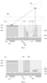
- the arrow line in FIG 1 indicates a direction of a light path.
- the embodiments of the present application disclose a packaging structure, which includes a substrate 100, and a light emitting element 200, a photosensitive element 300, a light-transmitting package body 400, and a reflector 600 that are disposed on a same side of the substrate 100.
- the substrate 100 provides an mounting basis for the light emitting element 200, the photosensitive element 300, the light-transmitting package body 400, and the reflector 600.
- the light emitting element 200, the photosensitive element 300, the light-transmitting package body 400, and the reflector 600 are all disposed on the same side of the substrate 100, and the light-transmitting package body 400 encloses the light emitting element 200, the light-sensitive element 300, and the reflector 600.
- the light-transmitting package body 400 can be a solid substance solidified from a liquid substance during packaging, or can be a solid-liquid mixture or other forms of substances. Compared with other forms of substances, solid substances basically have no fluidity, which can make the position of each device relatively fixed and improves the reliability of the packaging structure.
- the light-transmitting package body 400 may be epoxy resin glue, which has strong light transmittance, can reduce the loss when light passes through the light-transmitting package body 400, and has a better packaging effect.
- the light emitting element 200 can emit light, and the light can be emitted through the light-transmitting package body 400.
- the emitted light passes through the cover plate 940 and reaches the surface of the object 950, the emitted light is reflected by the object 950, and the reflected light can pass through the cover plate 940 and enter the light-transmitting package body 400 and reach the photosensitive element 300.
- the photosensitive element 300 can receive this part of light and perform corresponding processing (such as photoelectric conversion) to obtain required information.
- the light emitting element 200 is located between the reflector 600 and the photosensitive element 300.
- the side of the light emitting element 200 away from the photosensitive element 300 has a light emitting surface 210.
- the reflector 600 has a reflective surface 610 facing the light emitting element 200.
- the light emitted by the light emitting element 200 is reflected by the reflective surface 610 to the outside of the packaging structure, and the photosensitive element 300 receives the light reflected back from the outside of the packaging structure.
- the light emitted by the light emitting element 200 through the light emitting surface 210 needs to pass through the cover plate 940 to irradiate the object 950.
- the object 950 is located outside the packaging structure.
- the reflective surface 610 of the reflector 600 can change the path of the light emitted by the light emitting element 200, so that the light better satisfies the requirement on the light emitting direction, and more accurately illuminates the object 950.
- the light emitted by the light emitting element 200 passes through the light emitting surface 210 on the side away from the photosensitive element 300 to reach the reflective surface 610 on the side of the reflector 600 facing the light emitting element 200, the reflective surface 610 then reflects the light to the outside of the packaging structure, and after the light is reflected by an external object, the photosensitive element 300 receives the light reflected from the outside of the packaging structure, so as to complete corresponding processing.
- this method can change the direction of light emission, so that the light emitted by the light emitting element 200 is far away from the photosensitive element 300, thereby preventing light crosstalk. Therefore, there is no need to dispose a complex light blocking structure with a large space and the packaging structure has a smaller size.
- a side of the substrate 100 away from the light emitting element 200 is provided with a first pad 910, and the packaging structure can be mounted through the first pad 910, for example, the packaging structure can be mounted on a circuit board of an electronic device through the first pad 910.
- the light emitting surface 210 forms a non-zero angle with the substrate 100. That is, the light emitting surface 210 can be inclined relative to the substrate 100, so as to properly increase the distance between the light emitted by the light emitting element 200 and the photosensitive element 300, so as to better prevent light crosstalk.
- the angle at which the light emitting surface is inclined relative to the substrate 100 may be 45° to 60°. On the one hand, this angle range can make the light emitted by the light emitting element 200 farther away from the photosensitive element 300. On the other hand, this ensures that the propagation path of the light emitted by the light emitting element 200 is not excessively long, thereby reducing light loss and improving the optical performance of the packaging structure.
- the packaging structure further includes a first carrier 500, and the light emitting element 200 is disposed on a side of the first carrier 500 away from the photosensitive element 300.
- the first carrier 500 can appropriately raise the light emitting element 200, so that the light emitted by the light emitting element 200 is emitted through a shorter path, thereby reducing light loss, improving optical performance of the packaging structure, and further preventing the optical crosstalk in the packaging structure.
- the first carrier 500 may be a light shielding structure.
- the first carrier 500 may be a component made of opaque material, which can prevent light from penetrating.
- the first carrier 500 is disposed between the light emitting element 200 and the photosensitive element 300, and can prevent the light emitted by the light emitting element 200 from directly irradiating the photosensitive element 300, or intersecting with the light received by the photosensitive element 300 to avoid light crosstalk.
- higher light shielding requirements can be met only by using the first carrier 500, and the space occupied by the first carrier 500 is smaller. Therefore, the size of the entire packaging structure is smaller.
- the first carrier 500 is provided with a groove, and the light emitting element 200 is at least partially located in the groove.
- the light emitting element 200 is at least partially located in the groove, which can reduce the extra space occupied by the light emitting element 200 and facilitate the packaging of the light-transmitting package body 400.
- the groove can also assist in restricting the position of the light emitting element 200, so that the light emitting element 200 is not easy to be displaced relative to the first carrier 500, so that its position accuracy is higher.
- the light emitting element 200 is at least partially recessed relative to the first carrier 500, so that the distance between the light emitting surface 210 of the light emitting element 200 and the first carrier 500 is closer, and more light emitted by the light emitting element 200 can be blocked by the first carrier 500, thereby improving the light blocking effect of the first carrier 500.
- the light emitting element 200 is electrically connected to the substrate 100 through the first carrier 500, that is, an electrical connection structure may be provided in the first carrier 500, so that the light emitting element 200 is electrically connected to the substrate 100 through the electrical connection structure.
- the light emitting element 200 is electrically connected to the substrate 100 through a first conductor 700, where the first conductor 700 is located outside the first carrier 500.
- the electrical connection of the light emitting element 200 to the substrate 100 through the first carrier 500 can reduce the number of components in the packaging structure and make the structure of the packaging structure simpler.
- the light emitting element 200 is electrically connected to the substrate 100 through the first conductor 700, which can simplify the manner of electrical conduction between the light emitting element 200 and the substrate 100.
- the first carrier 500 can be connected to the substrate 100 through the second pad 920, and the second pad 920 can realize the mechanical connection between the first carrier 500 and the substrate 100, and can also realize the electrical connection between the first carrier 500 and the substrate 100.
- the photosensitive element 300 has a first top surface 310, the first top surface 310 is a surface of the photosensitive element 300 away from the substrate 100, the light-transmitting package body 400 has a second top surface 410, and the second top surface 410 is a surface of the light-transmitting package body 400 away from the substrate 100.
- the first top surface 310 may be lower than the second top surface 410, higher than the second top surface 410, or be flush with the second top surface 410. When the first top surface 310 is lower than the second top surface 410, the position of the photosensitive element 300 is lower, and its ability to receive light is poorer.
- the photosensitive element 300 When the first top surface 310 is higher than the second top surface 410, the photosensitive element 300 is at least partially located outside the light-transmitting package body 400, and the packaging effect is poorer. When the first top surface 310 is flush with the second top surface 410, this can increase the amount of light that the photosensitive element 300 can receive, thereby improving the light receiving efficiency of the photosensitive element 300, the packaging effect can be improved, and the size of the package structure can be minimized.
- the packaging structure further includes a second carrier 800, the second carrier 800 is disposed on the substrate 100, and the photosensitive element 300 is disposed on a side of the second carrier 800 away from the substrate 100.
- the position of the photosensitive element 300 has a crucial influence on its light receiving efficiency.
- the second carrier 800 is added, the height of the photosensitive element 300 relative to the substrate 100 can be appropriately increased, so that the distance between the photosensitive element 300 and the light can be closer to receive more light.
- the photosensitive element 300 is raised by the second carrier 800, other parts of the packaging structure of the packaging device are less likely to prevent the light from irradiating the photosensitive element 300. Therefore, this embodiment can further improve the light receiving efficiency of the photosensitive element 300.
- the photosensitive element 300 is electrically connected to the substrate 100 through the second carrier 800, that is, an electrical connection structure may be provided in the second carrier 800, so that the photosensitive element 300 is electrically connected to the substrate 100 through the electrical connection structure.
- the photosensitive element 300 is electrically connected to the substrate 100 through a second conductor, where the second conductor is located outside the first carrier 500.
- the electrical connection of the photosensitive element 300 to the substrate 100 through the second carrier 800 can reduce the number of components in the packaging structure and make the structure of the packaging structure simpler.
- the photosensitive element 300 is electrically connected to the substrate 100 through the second conductor, which can simplify the electrical conduction between the photosensitive element 300 and the substrate 100.
- the second carrier 800 can be connected to the substrate 100 through the third pad 930, and the third pad 930 can realize the mechanical connection between the second carrier 800 and the substrate 100, and can also realize the electrical connection between the second carrier and the substrate.
- the substrate 100 is provided with a first positioning part 110, and the reflector 600 is disposed on the first positioning part 110.
- the first positioning part 110 herein has the function of pre-positioning.
- the reflector 600 is directly fixed on the first positioning part 110. This arrangement not only facilitates the mounting of the reflector 600, improves the mounting efficiency of the reflector 600, and makes the position of the reflector 600 relative to the substrate 100 more accurate, improving the quality of the packaging device.
- the reflector 600 can be fixed on the first positioning part 110 through a first bonding part 960.
- This connection method can simplify the mounting operation of the reflector 600 and the first positioning part 110, and can also improve the mounting reliability of the reflector and the first positioning part.
- the first carrier 500 is located between the light emitting element 200 and the photosensitive element 300, and the light emitting element 200 has a light emitting surface 210 parallel to the substrate 100.
- the first carrier 500, the light emitting element 200 and the photosensitive element 300 are relatively independent, and each of the three is connected to the substrate 100.
- the light emitting element 200 and the first carrier 500 may be in direct contact or have a gap. Light can be reliably shielded by the first carrier 500, and therefore the structure of the packaging structure in this solution is simpler.
- the light emitting element 200 can be electrically connected to the substrate 100 through the pad, or can be electrically connected to the substrate 100 through the first conductor 700.
- the substrate 100 can be provided with a second positioning part 120, and the first carrier 500 can be fixed on the second positioning part 120 through the second bonding part 970, so as to connect the first carrier 500 and the substrate 100.
- the substrate 100 can be provided with a third positioning part 130, and the light emitting element 200 is fixed on the third positioning part 130 through the third bonding part 980, so as to connect the light emitting element 200 and the substrate 100.
- the embodiment of the present application also discloses an electronic device, which includes a circuit board and a packaging structure disposed on the circuit board, and the packaging structure is the packaging structure in any one of the above-mentioned embodiments.
- the electronic device in this embodiment of this application may be a device, such as a smart phone, a tablet computer, an e-book reader, a wearable device (for example, a smart watch), and a video game console.
- the embodiments of this application do not limit the specific type of the electronic device.
Landscapes
- Physics & Mathematics (AREA)
- General Physics & Mathematics (AREA)
- Led Device Packages (AREA)
- Photo Coupler, Interrupter, Optical-To-Optical Conversion Devices (AREA)
Applications Claiming Priority (2)
| Application Number | Priority Date | Filing Date | Title |
|---|---|---|---|
| CN202011192715.3A CN112310062B (zh) | 2020-10-30 | 2020-10-30 | 封装结构及电子设备 |
| PCT/CN2021/126317 WO2022089401A1 (zh) | 2020-10-30 | 2021-10-26 | 封装结构及电子设备 |
Publications (2)
| Publication Number | Publication Date |
|---|---|
| EP4239678A1 true EP4239678A1 (de) | 2023-09-06 |
| EP4239678A4 EP4239678A4 (de) | 2024-05-01 |
Family
ID=74332870
Family Applications (1)
| Application Number | Title | Priority Date | Filing Date |
|---|---|---|---|
| EP21885128.5A Pending EP4239678A4 (de) | 2020-10-30 | 2021-10-26 | Verkapselungsstruktur und elektronische vorrichtung |
Country Status (5)
| Country | Link |
|---|---|
| US (1) | US20230261150A1 (de) |
| EP (1) | EP4239678A4 (de) |
| JP (1) | JP7504297B2 (de) |
| CN (1) | CN112310062B (de) |
| WO (1) | WO2022089401A1 (de) |
Families Citing this family (2)
| Publication number | Priority date | Publication date | Assignee | Title |
|---|---|---|---|---|
| CN112310062B (zh) * | 2020-10-30 | 2022-09-09 | 维沃移动通信有限公司 | 封装结构及电子设备 |
| CN114244984B (zh) * | 2021-12-16 | 2024-03-26 | 维沃移动通信有限公司 | 液态镜头模组及电子设备 |
Family Cites Families (24)
| Publication number | Priority date | Publication date | Assignee | Title |
|---|---|---|---|---|
| JP2001156325A (ja) | 1999-11-29 | 2001-06-08 | Citizen Electronics Co Ltd | フォトリフレクター |
| US20030111588A1 (en) * | 2001-12-18 | 2003-06-19 | Pao-Jung Chen | Near-contact optical touch-screen sensor module |
| CN100470847C (zh) * | 2006-01-13 | 2009-03-18 | 崴强科技股份有限公司 | 影像感测芯片封装装置 |
| JP4808660B2 (ja) | 2007-03-16 | 2011-11-02 | 株式会社フジクラ | 光送受信モジュールとその製造方法 |
| JP2009038098A (ja) | 2007-07-31 | 2009-02-19 | Rohm Co Ltd | 受発光デバイス及びその製造方法 |
| JP2009088433A (ja) | 2007-10-03 | 2009-04-23 | Citizen Electronics Co Ltd | フォトリフレクタ |
| CN101158464B (zh) * | 2007-10-19 | 2010-06-09 | 友达光电股份有限公司 | 光源装置及其所构成的背光模组 |
| JP2011096724A (ja) | 2009-10-27 | 2011-05-12 | Sharp Corp | 反射型光結合装置および電子機器 |
| CN102880342B (zh) * | 2012-09-05 | 2018-04-06 | 惠州Tcl移动通信有限公司 | 一种距离传感器组件及移动通信设备 |
| US9263618B2 (en) * | 2013-03-05 | 2016-02-16 | Apple Inc. | Proximity sensor module with light reflector |
| US9590129B2 (en) * | 2014-11-19 | 2017-03-07 | Analog Devices Global | Optical sensor module |
| US10429509B2 (en) * | 2014-12-24 | 2019-10-01 | Stmicroelectronics Pte Ltd. | Molded proximity sensor |
| KR20160103415A (ko) * | 2015-02-24 | 2016-09-01 | 엘지이노텍 주식회사 | 근접센서와 이를 포함하는 카메라 모듈과 이를 포함하는 이동 단말기 |
| KR102475651B1 (ko) | 2015-12-30 | 2022-12-09 | 엘지이노텍 주식회사 | 인체 착용장치 및 이의 동작 방법 |
| EP3214462B1 (de) * | 2016-03-04 | 2021-04-28 | ams AG | Optische sensoranordnung |
| CN106453725B (zh) * | 2016-12-06 | 2023-04-07 | Oppo广东移动通信有限公司 | 一种终端 |
| CN106847802B (zh) * | 2016-12-29 | 2019-09-24 | 矽力杰半导体技术(杭州)有限公司 | 光学传感器封装组件及其制作方法和电子设备 |
| JP6630309B2 (ja) * | 2017-04-10 | 2020-01-15 | キヤノン株式会社 | 光学センサ及び画像形成装置 |
| CN107968884B (zh) * | 2017-11-22 | 2020-05-12 | Oppo广东移动通信有限公司 | 电子设备 |
| US11287312B2 (en) * | 2018-05-09 | 2022-03-29 | Advanced Semiconductor Engineering, Inc. | Optical system and method of manufacturing the same |
| CN108711566B (zh) * | 2018-05-25 | 2024-05-24 | 南京矽力微电子技术有限公司 | 光学感测系统、光学感测组件及其制造方法 |
| CN108493185A (zh) * | 2018-05-25 | 2018-09-04 | 矽力杰半导体技术(杭州)有限公司 | 光学感测系统和电子显示系统 |
| US20220140172A1 (en) * | 2020-03-25 | 2022-05-05 | Sensortek Technology Corp. | Light sensing device packaging structure and packaging method thereof |
| CN112310062B (zh) * | 2020-10-30 | 2022-09-09 | 维沃移动通信有限公司 | 封装结构及电子设备 |
-
2020
- 2020-10-30 CN CN202011192715.3A patent/CN112310062B/zh active Active
-
2021
- 2021-10-26 JP JP2023526448A patent/JP7504297B2/ja active Active
- 2021-10-26 EP EP21885128.5A patent/EP4239678A4/de active Pending
- 2021-10-26 WO PCT/CN2021/126317 patent/WO2022089401A1/zh not_active Ceased
-
2023
- 2023-04-28 US US18/309,485 patent/US20230261150A1/en active Pending
Also Published As
| Publication number | Publication date |
|---|---|
| EP4239678A4 (de) | 2024-05-01 |
| WO2022089401A1 (zh) | 2022-05-05 |
| CN112310062A (zh) | 2021-02-02 |
| CN112310062B (zh) | 2022-09-09 |
| JP2023547258A (ja) | 2023-11-09 |
| JP7504297B2 (ja) | 2024-06-21 |
| US20230261150A1 (en) | 2023-08-17 |
Similar Documents
| Publication | Publication Date | Title |
|---|---|---|
| US20230261150A1 (en) | Packaging structure and electronic device | |
| US9554025B2 (en) | Solid state image capturing apparatus, camera module and electronic device including anti-reflection plate | |
| US7026654B2 (en) | Package for optical semiconductor | |
| US20200335539A1 (en) | Photosensitive module | |
| US11348977B2 (en) | Display panel and electronic device | |
| CN111653447A (zh) | 电路结构、应用其的背光模块及发光按键装置 | |
| EP3822738B1 (de) | Bildschirmanordnung, elektronische vorrichtung und steuerverfahren für eine elektronische vorrichtung | |
| CN108666281A (zh) | 光学器件封装结构及移动终端 | |
| CN112310126A (zh) | 光学距离传感模组及其加工方法、电子设备 | |
| CN108333639A (zh) | 接近传感器的改良结构 | |
| CN112382211B (zh) | 显示元件及具有该显示元件的终端 | |
| CN113099005B (zh) | 电子设备 | |
| JP7072486B2 (ja) | 近接センサ用パッケージ、近接センサ装置および電子モジュール | |
| US20200111931A1 (en) | Wafer level sensing module, manufacturing method thereof and electronic device using the same | |
| CN111221177A (zh) | 背光模组及电子设备 | |
| CN109244093B (zh) | 一种光学封装组件及移动终端 | |
| WO2022161333A1 (zh) | 电子设备及显示装置 | |
| US6229223B1 (en) | Flexible printed board | |
| CN116779627A (zh) | 封装结构及其制作方法 | |
| JP2000114588A (ja) | 光伝送素子 | |
| CN111510615B (zh) | 一种摄像模组及电子设备 | |
| US6311023B1 (en) | Camera having a light-shieldable member for protecting a semiconductor element flip-chip-bonded on a flexible printed board | |
| US12622091B2 (en) | Light-emitting photosensitive sensor structure and manufacturing method thereof | |
| CN114895475B (zh) | 一种显示装置 | |
| CN212749868U (zh) | 指纹识别装置和电子设备 |
Legal Events
| Date | Code | Title | Description |
|---|---|---|---|
| STAA | Information on the status of an ep patent application or granted ep patent |
Free format text: STATUS: THE INTERNATIONAL PUBLICATION HAS BEEN MADE |
|
| PUAI | Public reference made under article 153(3) epc to a published international application that has entered the european phase |
Free format text: ORIGINAL CODE: 0009012 |
|
| STAA | Information on the status of an ep patent application or granted ep patent |
Free format text: STATUS: REQUEST FOR EXAMINATION WAS MADE |
|
| 17P | Request for examination filed |
Effective date: 20230519 |
|
| AK | Designated contracting states |
Kind code of ref document: A1 Designated state(s): AL AT BE BG CH CY CZ DE DK EE ES FI FR GB GR HR HU IE IS IT LI LT LU LV MC MK MT NL NO PL PT RO RS SE SI SK SM TR |
|
| DAV | Request for validation of the european patent (deleted) | ||
| DAX | Request for extension of the european patent (deleted) | ||
| A4 | Supplementary search report drawn up and despatched |
Effective date: 20240402 |
|
| RIC1 | Information provided on ipc code assigned before grant |
Ipc: G01D 5/26 20060101ALI20240325BHEP Ipc: H01L 33/60 20100101ALI20240325BHEP Ipc: H01L 31/12 20060101ALI20240325BHEP Ipc: H01L 31/0232 20140101ALI20240325BHEP Ipc: H01L 25/16 20060101AFI20240325BHEP |