EP4239651B1 - Perovskit-radiovoltaik-fotovoltaikbatterie - Google Patents
Perovskit-radiovoltaik-fotovoltaikbatterie Download PDFInfo
- Publication number
- EP4239651B1 EP4239651B1 EP21964974.6A EP21964974A EP4239651B1 EP 4239651 B1 EP4239651 B1 EP 4239651B1 EP 21964974 A EP21964974 A EP 21964974A EP 4239651 B1 EP4239651 B1 EP 4239651B1
- Authority
- EP
- European Patent Office
- Prior art keywords
- transport layer
- electrode
- charge transport
- perovskite
- compound
- Prior art date
- Legal status (The legal status is an assumption and is not a legal conclusion. Google has not performed a legal analysis and makes no representation as to the accuracy of the status listed.)
- Active
Links
Images
Classifications
-
- G—PHYSICS
- G21—NUCLEAR PHYSICS; NUCLEAR ENGINEERING
- G21H—OBTAINING ENERGY FROM RADIOACTIVE SOURCES; APPLICATIONS OF RADIATION FROM RADIOACTIVE SOURCES, NOT OTHERWISE PROVIDED FOR; UTILISING COSMIC RADIATION
- G21H1/00—Arrangements for obtaining electrical energy from radioactive sources, e.g. from radioactive isotopes, nuclear or atomic batteries
- G21H1/06—Cells wherein radiation is applied to the junction of different semiconductor materials
-
- G—PHYSICS
- G21—NUCLEAR PHYSICS; NUCLEAR ENGINEERING
- G21H—OBTAINING ENERGY FROM RADIOACTIVE SOURCES; APPLICATIONS OF RADIATION FROM RADIOACTIVE SOURCES, NOT OTHERWISE PROVIDED FOR; UTILISING COSMIC RADIATION
- G21H1/00—Arrangements for obtaining electrical energy from radioactive sources, e.g. from radioactive isotopes, nuclear or atomic batteries
- G21H1/04—Cells using secondary emission induced by alpha radiation, beta radiation, or gamma radiation
-
- G—PHYSICS
- G21—NUCLEAR PHYSICS; NUCLEAR ENGINEERING
- G21H—OBTAINING ENERGY FROM RADIOACTIVE SOURCES; APPLICATIONS OF RADIATION FROM RADIOACTIVE SOURCES, NOT OTHERWISE PROVIDED FOR; UTILISING COSMIC RADIATION
- G21H1/00—Arrangements for obtaining electrical energy from radioactive sources, e.g. from radioactive isotopes, nuclear or atomic batteries
- G21H1/12—Cells using conversion of the radiation into light combined with subsequent photoelectric conversion into electric energy
-
- H—ELECTRICITY
- H10—SEMICONDUCTOR DEVICES; ELECTRIC SOLID-STATE DEVICES NOT OTHERWISE PROVIDED FOR
- H10K—ORGANIC ELECTRIC SOLID-STATE DEVICES
- H10K30/00—Organic devices sensitive to infrared radiation, light, electromagnetic radiation of shorter wavelength or corpuscular radiation
- H10K30/40—Organic devices sensitive to infrared radiation, light, electromagnetic radiation of shorter wavelength or corpuscular radiation comprising a p-i-n structure, e.g. having a perovskite absorber between p-type and n-type charge transport layers
-
- H—ELECTRICITY
- H10—SEMICONDUCTOR DEVICES; ELECTRIC SOLID-STATE DEVICES NOT OTHERWISE PROVIDED FOR
- H10K—ORGANIC ELECTRIC SOLID-STATE DEVICES
- H10K30/00—Organic devices sensitive to infrared radiation, light, electromagnetic radiation of shorter wavelength or corpuscular radiation
- H10K30/50—Photovoltaic [PV] devices
-
- H—ELECTRICITY
- H10—SEMICONDUCTOR DEVICES; ELECTRIC SOLID-STATE DEVICES NOT OTHERWISE PROVIDED FOR
- H10K—ORGANIC ELECTRIC SOLID-STATE DEVICES
- H10K30/00—Organic devices sensitive to infrared radiation, light, electromagnetic radiation of shorter wavelength or corpuscular radiation
- H10K30/80—Constructional details
- H10K30/81—Electrodes
- H10K30/82—Transparent electrodes, e.g. indium tin oxide [ITO] electrodes
-
- H—ELECTRICITY
- H10—SEMICONDUCTOR DEVICES; ELECTRIC SOLID-STATE DEVICES NOT OTHERWISE PROVIDED FOR
- H10K—ORGANIC ELECTRIC SOLID-STATE DEVICES
- H10K71/00—Manufacture or treatment specially adapted for the organic devices covered by this subclass
- H10K71/10—Deposition of organic active material
- H10K71/16—Deposition of organic active material using physical vapour deposition [PVD], e.g. vacuum deposition or sputtering
-
- H—ELECTRICITY
- H10—SEMICONDUCTOR DEVICES; ELECTRIC SOLID-STATE DEVICES NOT OTHERWISE PROVIDED FOR
- H10K—ORGANIC ELECTRIC SOLID-STATE DEVICES
- H10K71/00—Manufacture or treatment specially adapted for the organic devices covered by this subclass
- H10K71/60—Forming conductive regions or layers, e.g. electrodes
-
- H—ELECTRICITY
- H10—SEMICONDUCTOR DEVICES; ELECTRIC SOLID-STATE DEVICES NOT OTHERWISE PROVIDED FOR
- H10K—ORGANIC ELECTRIC SOLID-STATE DEVICES
- H10K85/00—Organic materials used in the body or electrodes of devices covered by this subclass
- H10K85/50—Organic perovskites; Hybrid organic-inorganic perovskites [HOIP], e.g. CH3NH3PbI3
-
- H—ELECTRICITY
- H10—SEMICONDUCTOR DEVICES; ELECTRIC SOLID-STATE DEVICES NOT OTHERWISE PROVIDED FOR
- H10K—ORGANIC ELECTRIC SOLID-STATE DEVICES
- H10K2101/00—Properties of the organic materials covered by group H10K85/00
- H10K2101/30—Highest occupied molecular orbital [HOMO], lowest unoccupied molecular orbital [LUMO] or Fermi energy values
-
- H—ELECTRICITY
- H10—SEMICONDUCTOR DEVICES; ELECTRIC SOLID-STATE DEVICES NOT OTHERWISE PROVIDED FOR
- H10K—ORGANIC ELECTRIC SOLID-STATE DEVICES
- H10K2101/00—Properties of the organic materials covered by group H10K85/00
- H10K2101/40—Interrelation of parameters between multiple constituent active layers or sublayers, e.g. HOMO values in adjacent layers
-
- Y—GENERAL TAGGING OF NEW TECHNOLOGICAL DEVELOPMENTS; GENERAL TAGGING OF CROSS-SECTIONAL TECHNOLOGIES SPANNING OVER SEVERAL SECTIONS OF THE IPC; TECHNICAL SUBJECTS COVERED BY FORMER USPC CROSS-REFERENCE ART COLLECTIONS [XRACs] AND DIGESTS
- Y02—TECHNOLOGIES OR APPLICATIONS FOR MITIGATION OR ADAPTATION AGAINST CLIMATE CHANGE
- Y02E—REDUCTION OF GREENHOUSE GAS [GHG] EMISSIONS, RELATED TO ENERGY GENERATION, TRANSMISSION OR DISTRIBUTION
- Y02E10/00—Energy generation through renewable energy sources
- Y02E10/50—Photovoltaic [PV] energy
- Y02E10/549—Organic PV cells
Definitions
- the present invention relates to a perovskite radiovoltaic-photovoltaic battery and a method for manufacturing same.
- a photovoltaic battery is a photoelectric converting device that converts light energy into electrical energy, which has a high energy conversion effect.
- the photovoltaic battery enables the effective use of clean and non-polluting solar energy.
- the photovoltaic battery is greatly affected by weather and season.
- a nuclear battery also referred to as an isotope battery, is a device that converts the energy released from the decay of a radioactive isotope into electrical energy. It has the advantages, such as a long service life, an excellent environmental stability and an enough small size, but the energy conversion efficiency thereof is low.
- Nuclear battery converts energy in multiple manners.
- the nuclear battery that converts the energy of high-energy particles from radioactive sources into photogenerated carriers by means of the photoelectric effect and forms power output by PN junction or PIN junction is referred to as a radio-voltaic nuclear battery (referred as a radiovoltaic battery hereinbelow for short).
- the working principle thereof is similar to that of a photovoltaic battery.
- radiovoltaic-photovoltaic battery with an excellent environmental stability and a high energy conversion efficiency can be realized.
- Prior art perovskite nuclear batteries are known for example from patents CN 107093486 A or CN 111261311 B .
- the present invention has been made with an objective to provide a perovskite radiovoltaic-photovoltaic battery, which can converts both isotopic decay particles or other energy particles and solar energy into electrical energy, thus reducing the influence of light conditions, achieving an enhanced environmental stability, and being able to improve the energy conversion efficiency.
- Another objective of the present invention is also to provide a method for manufacturing a perovskite radiovoltaic-photovoltaic battery. The method can reduce the procedures for battery manufacturing and improve the production efficiency.
- a first aspect of the present invention provides a perovskite radiovoltaic-photovoltaic battery having a first electrode, a first charge transport layer, a perovskite layer, a second charge transport layer, and a second electrode in sequence, wherein the first electrode is a transparent electrode, the first charge transport layer is an electron transport layer and the second charge transport layer is a hole transport layer, or the first charge transport layer is a hole transport layer and the second charge transport layer is an electron transport layer, and the second electrode is a radiating electrode formed by compounding a radioactive source with an electrical conductor material.
- the radioactive source is selected from at least one of an ⁇ -type radioactive source, a ⁇ -type radioactive source, an X-ray radioactive source and a ⁇ -ray radioactive source.
- the ⁇ -type radioactive source is selected from at least one of 210 Po or a compound thereof, 228 Th or a compound thereof, 235 U or a compound thereof, 238 Pu or a compound thereof, 238 PuO 2 microsphere, 241 Am or a compound thereof, 242 Cm or a compound thereof, and 244 Cm or a compound thereof; and the ⁇ -type radioactive source is selected from at least one of (C 4 H 3 3 H 5 -) n , 3 H 2 , Ti 3 H 4 , 14 C or a compound thereof, 35 S or a compound thereof, 63 Ni or a compound thereof, 90 Sr or a compound thereof, 90 Sr/ 90 Y, 99 Tc or a compound thereof, 106 Ru or a compound thereof, 137 Cs or a compound thereof, 144 Ce or a compound thereof, 147 Pm or a compound thereof, 151 Sm or a compound thereof, and 226 Ra or a compound thereof.
- the radioactive source is preferably a ⁇ -type radioactive source, and more preferably is selected from at least one of Ti 3 H 4 , 63 Ni, and 90 Sr/ 90 Y.
- the content of the radioactive source in the radiating electrode is no more than 90 wt%, and preferably 5-30 wt%.
- the first charge transport layer and the second charge transport layer has a semiconductor material of at least one of the following materials and derivatives thereof: an imide compound, a quinone compound, fullerene and a derivative thereof, poly[bis(4-phenyl)(2,4,6-trimethylphenyl)amine], 2,2',7,7'-tetra(N,N-p-methoxyanilino)-9,9'-spirobifluorene, methoxytriphenylamine-fluoroformamidine, poly (3,4-ethylenedioxythiophene): polystyrene sulfonic acid, poly-3-hexylthiophene, triptycene-cored triphenylamine, 3,4-ethylenedioxythiophene-methoxytriphenylamine, N-(4-aniline)carbazole-spirobifluorene, polythiophene, a metal oxide (with the metal element being selected from Mg, Ni,
- the electrical conductor material of the first electrode and the second electrode is an organic electrically conductive material, an inorganic electrically conductive material, or an electrically conductive material obtained by mixing an organic electrically conductive material and an inorganic electrically conductive material;
- the organic electrically conductive material is selected from at least one of a polymer of (3,4-ethylenedioxythiophene monomer), polythiophene, polyacetylene, polypyrrole, polyphenylene, polyphenylacetylene, polyaniline, an epoxy resin, a phenolic resin, and polypropylene
- the inorganic electrically conductive material is selected from at least one of a transparent conductive oxide, a metal, and a carbon derivative.
- the perovskite in the perovskite layer has a chemical formula of ABX 3 , where A is selected from at least one of an methylamine cation of MA + , a formamidine cation of FA + , and a cesium cation of Cs + , B is selected from at least one of a lead cation of Pb 2+ and a tin cation of Sn 2+ , and X is a halide ion, COO - or a mixed anion thereof.
- the first electrode has a thickness of 50 nm - 1000 nm; and/or the first charge transport layer has a thickness of 10 nm - 1000 nm; and/or the perovskite layer has a thickness of 50 nm - 2000 nm; and/or the second charge transport layer has a thickness of 10 nm - 1000 nm; and/or the second electrode has a thickness of 10 nm - 500 nm.
- the difference between the Fermi level of the second electrode and the conduction band bottom energy level of the second charge transport layer is -1.0-1.0 eV
- the difference between the Fermi level of the second electrode and the valence band top energy level of the second charge transport layer is ⁇ 1.0 eV.
- the difference between the Fermi level of the second electrode and the valence band top energy level of the second charge transport layer is -1.0-1.0 eV
- the difference between the Fermi level of the second electrode and the conduction band bottom energy level of the second charge transport layer is ⁇ -1.0 eV.
- a second aspect of the present invention provides a method for manufacturing a perovskite radiovoltaic-photovoltaic battery, which is used to manufacture the perovskite radiovoltaic-photovoltaic battery of the present invention.
- the method for manufacturing a perovskite radiovoltaic-photovoltaic battery of the present invention includes: a procedure of forming a first charge transport layer on a first electrode; a procedure of forming a perovskite layer on the first charge transport layer; a procedure of forming a second charge transport layer on the perovskite layer; and a procedure of forming a second electrode on the second charge transport layer; wherein the second electrode is formed by compounding a radioactive source with an electrical conductor material by means of a process selected from at least one of chemical bath deposition, electrochemical deposition, chemical vapor deposition, physical epitaxial growth, thermal evaporation co-evaporation, atomic layer deposition, magnetron sputtering, precursor solution spin coating, precursor solution s
- the second electrode is formed by compounding a radioactive source with an electrical conductor material by at least one process of thermal evaporation co-evaporation, magnetron sputtering, and precursor solution spin coating.
- a perovskite radiovoltaic-photovoltaic battery having a first electrode, a first charge transport layer, a perovskite layer, a second charge transport layer, and a second electrode in sequence
- the second electrode is a radiating electrode formed by compounding an electrical conductor material with a radioactive source
- the perovskite radiovoltaic-photovoltaic battery of the present invention can convert both isotopic decay particles or other energy particles and solar energy into electrical energy and can improve the energy conversion efficiency.
- the second electrode is formed by compounding an electrical conductor material with a radioactive source, which can reduce the number of hetero-interfaces in the structure of the battery, thus improving the performance of the battery.
- the second electrode is formed by compounding a radioactive source with an electrical conductor material, which can reduce the procedures for battery manufacturing and improve the production efficiency.
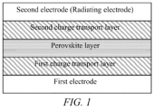
- Fig. 1 is a schematic diagram showing the structure of the perovskite radiovoltaic-photovoltaic battery of the present invention.
- a perovskite radiovoltaic-photovoltaic battery is provided.
- the perovskite radiovoltaic-photovoltaic battery is as shown in Fig. 1 , which has a first electrode, a first charge transport layer, a perovskite layer, a second charge transport layer, and a second electrode in sequence.
- the first electrode is a transparent electrode, which can allow sunlight to income from the first electrode, and the perovskite radiovoltaic-photovoltaic battery of the present invention can use the incident sunlight from the first electrode for converting light energy into electrical energy.
- the first charge transport layer is an electron transport layer and the second charge transport layer is a hole transport layer, or the first charge transport layer is a hole transport layer and the second charge transport layer is an electron transport layer.
- the first charge transport layer, the perovskite layer, and the second charge transport layer together form a PIN-structured functional layer of the battery.
- the second electrode is a radiating electrode formed by compounding a radioactive source with an electrical conductor material.
- the second electrode radioactive, the high-energy particles generated from the radioactive source can be absorbed by the perovskite layer for energy conversion in the PIN-structured functional layer of the battery.
- the second electrode is formed by compounding a radioactive source with an electrical conductor material, and thus the number of hetero-interfaces in the structure of the battery can be reduced, such that the redundant interface matching and the occurrence of interface defects are reduced, the redundant series resistance can also be lowered, and the charge transport efficiency in the device is improved, thereby improving the performance of the battery.
- the second electrode formed by compounding a radioactive source with an electrical conductor material can reduce the structural volume of the second electrode, which is beneficial to the cascading of the battery and allows its flexible application in production; moreover, the process for other structures in the battery is not affected.
- the radioactive source may be selected from at least one of an ⁇ -type radioactive source, a ⁇ -type radioactive source, an X-ray radioactive source and a ⁇ -ray radioactive source.
- the ⁇ -type radioactive source may be selected from at least one of 210 Po or a compound thereof, 228 Th or a compound thereof, 235 U or a compound thereof, 238 Pu or a compound thereof, 238 PuO 2 microsphere, 241 Am or a compound thereof, 242 Cm or a compound thereof, and 244 Cm or a compound thereof; and the ⁇ -type radioactive source may be selected from at least one of (C 4 H 3 3 H 5 -) n , 3 H 2 , Ti 3 H 4 , 14 C or a compound thereof, 35 S or a compound thereof, 63 Ni or a compound thereof, 90 Sr or a compound thereof, 90 Sr/ 90 Y, 99 Tc or a compound thereof, 106 Ru or a compound thereof, 137 Cs or a compound thereof, 144 Ce or a compound thereof, 147 Pm or a compound thereof, 151 Sm or a compound thereof, and 226 Ra or a compound thereof.
- the radioactive source is preferably a ⁇ -type radioactive source, and more preferably is selected from at least one of Ti 3 H 4 , 63 Ni or a compound thereof, and 90 Sr/ 90 Y.
- the ⁇ -type radiative source is of a relatively low radiation particle energy and a high safety, it has small radiation effect on perovskite and other structures in the battery.
- the radioactive source is selected from at least one of Ti 3 H 4 , 63 Ni or a compound thereof, and 90 Sr/ 90 Y, the preparation process using same shows high compatibility and good controllability.
- the content of the radioactive source in the radiating electrode is no more than 90 wt%, and preferably 5-30 wt%.
- the perovskite substance in the perovskite layer of the perovskite radiovoltaic-photovoltaic battery of the present invention has a chemical formula of ABX 3 , where A is selected from at least one of a methylamine cation of MA + , a formamidine cation of FA + , and a cesium cation of Cs + , B is selected from at least one of a lead cation of Pb 2+ and a tin cation of Sn 2+ , and X is selected from at least one of a halide anion (F - , Cl - , Br - , and I - ), and COO - .
- Perovskite is used as an absorber material to adsorb sunlight and the radiation particles from the radioactive source.
- the semiconductor material of the charge transport layers is an n-type semiconductor material or a p-type semiconductor material; the first charge transport layer comprises an n-type semiconductor material and the second charge transport layer comprises a p-type semiconductor material, or the first charge transport layer comprises a p-type semiconductor material and the second charge transport layer comprises an n-type semiconductor material.
- examples can be at least one of the following materials and derivatives thereof: an imide compound, a quinone compound, fullerene (C60) and a derivative thereof, poly[bis(4-phenyl)(2,4,6-trimethylphenyl)amine] (PTAA), 2,2',7,7'-tetra(N,N-p-methoxyanilino)-9,9'-spirobifluorene (Spiro-OMeTAD), methoxytriphenylamine-fluoroformamidine (OMeTPA-FA), poly(3,4-ethylenedioxythiophene):polystyrene sulfonic acid (PE DOT : PSS), poly-3-hexylthiophene (P3HT), triptycene-cored triphenylamine (H101), 3,4-ethylenedioxythiophene-methoxytriphenylamine (EDOT-OMeTPA), N-(4
- the n-type semiconductor material is preferably tin dioxide, titanium dioxide, zinc oxide, C60, methyl [6,6]-phenyl-C61-butyrate, or methyl [6,6]-phenyl-C71-butyrate
- the p-type semiconductor material is preferably 2,2',7,7'-tetra(N,N-p-methoxyanilino)-9,9'-spirobifluorene, nickel oxide, poly[bis(4-phenyl)(2,4,6-trimethylphenyl)amine], and poly-3-hexylthiophene.
- the electrical conductor material of the first electrode and the second electrode is an organic electrically conductive material, an inorganic electrically conductive material, or an electrically conductive material obtained by mixing an organic electrically conductive material and an inorganic electrically conductive material; wherein the organic electrically conductive material is selected from at least one of a polymer of (3,4-ethylenedioxythiophene monomer), polythiophene, polyacetylene, polypyrrole, polyphenylene, polyphenylacetylene, polyaniline, an epoxy resin, a phenolic resin, and polypropylene, and the inorganic electrically conductive material is selected from at least one of a transparent conductive oxide (FTO, ITO, AZO, etc.), a metal, and a carbon derivative.
- a transparent conductive oxide FTO, ITO, AZO, etc.
- the first electrode has a thickness of 50 nm - 1000 nm; the first charge transport layer has a thickness of 10 nm - 1000 nm; the perovskite layer has a thickness of 50 nm - 2000 nm; the second charge transport layer has a thickness of 10 nm - 1000 nm; and the second electrode has a thickness of 10 nm - 500 nm.
- the difference between the Fermi level of the second electrode and the conduction band bottom energy level of the second charge transport layer is -1.0-1.0 eV, and the difference between the Fermi level of the second electrode and the valence band top energy level of the second charge transport layer is ⁇ 1.0 eV;
- the second charge transport layer is a hole transport layer, the difference between the Fermi level of the second electrode and the valence band top energy level of the second charge transport layer is -1.0-1.0 eV, and the difference between the Fermi level of the second electrode and the conduction band bottom energy level of the second charge transport layer is ⁇ -1.0 eV.
- the difference between the Fermi level of the electrode material and the conduction band bottom energy levels between the electron transport layer materials affects the high-efficient transfer of electrons.
- the second charge transport layer is an electron transport layer
- the difference between the Fermi level of the second electrode and the valence band top energy level of the second charge transport layer may be set to -1.0-1.0 eV, and the difference between the Fermi level of the second electrode and the conduction band bottom energy level of the second charge transport layer is set to a lager value, for example, no less than -1.0 eV.
- a reflective layer may be provided at an appropriate position.
- a reflective layer may be provided on the second electrode at the side opposite to the second charge transport layer. The provision of the reflective layer can further improve the energy utilization in the battery.
- a method for manufacturing a perovskite radiovoltaic-photovoltaic battery is provided.
- the method for manufacturing a perovskite radiovoltaic-photovoltaic battery of the present invention is used to manufacture the perovskite radiovoltaic-photovoltaic battery of the present invention, and the method includes: a procedure of forming a first charge transport layer on a first electrode; a procedure of forming a perovskite layer on the first charge transport layer; a procedure of forming a second charge transport layer on the perovskite layer; and a procedure of forming a second electrode on the second charge transport layer; wherein the second electrode is formed by compounding a radioactive source with an electrical conductor material by means of a process selected from at least one of chemical bath deposition, electrochemical deposition, chemical vapor deposition, physical epitaxial growth, thermal evaporation co-evaporation, atomic layer deposition, magnetron sputtering, precursor solution spin coating, precursor solution
- the second electrode is preferably formed by compounding by means of at least one process of thermal evaporation co-evaporation process, magnetron sputtering process, and precursor solution spin coating process.
- the second electrode is formed by compounding a radioactive source with an electrical conductor material, which can reduce the procedures for battery manufacturing and improve the production efficiency.
- a glass substrate with a specification of 2.0 cm ⁇ 2.0 cm that is covered with an FTO electrically conductive layer of 550 nm is provided; the surface of the FTO electrically conductive glass is sequentially washed with acetone and isopropanol twice, respectively; and then the substrate is immersed into deionized water for an ultrasonic treatment for 10 min, dried in a blast drying oven, and placed in a glove box (an N2 atmosphere), to obtain a first electrode.
- the FTO electrically conductive layer is spin-coated with a 3 wt% aqueous solution of SnO 2 nano-colloid by a spin coater (LEBO EZ6-S, the same below) at a rotation speed of 5000 rpm, and then heated on a constant-temperature heating table at 150°C for 15 min to obtain a first charge transport layer with a thickness of 30 nm.
- a spin coater LEBO EZ6-S, the same below
- the resulting first charge transport layer is spin-coated with an FAPbI 3 -DMF solution at a concentration of 1.5 mol/L by a spin coater at a speed of 4500 rpm, and then moved to a constant-temperature heating table and heated at 100°C for 30 min, and cooled to room temperature to form a perovskite layer with a thickness of 500 nm.
- the resulting perovskite layer is spin-coated with a chlorobenzene solution of Spiro-OMeTAD at a concentration of 73 mg/mL by a spin coater at a speed of 4000 rpm, and left to stand for 10-30 min at a normal temperature under an N 2 atmosphere to obtain a second charge transport layer with a thickness of 200 nm.
- the second charge transport layer is a hole transport layer.
- the sample that has been formed with the first electrode, the first charge transport layer, the perovskite layer and the second charge transport layer is placed in a vacuum coating machine, and under the vacuum conditions of 5 ⁇ 10 -4 Pa, 63 NiCl x and Ag are co-evaporated onto the surface of the resulting second charge transport layer at an evaporation speed ratio of 63 NiCl x to Ag of 0.1 : 1, so as to obtain a radioactive Ag electrode with a thickness of 80 nm as a second electrode.
- a sample that is formed, in the same manner as in example 1, with the first electrode, the first charge transport layer, the perovskite layer and the second charge transport layer is placed in a vacuum coating machine, and under the vacuum conditions of 5 ⁇ 10 -4 Pa, Ti 3 H 4 and Ag are co-evaporated onto the surface of the resulting second charge transport layer at an evaporation speed ratio of Ti 3 H 4 to Ag of 0.1 : 1, so as to obtain a radiating Ag electrode with a thickness of 80 nm as a second electrode.
- a first electrode is formed in the same manner as in example 1.
- the resulting FTO electrically conductive layer is spin-coated with an aqueous solution of NiOx nano-colloid at a concentration of 3 wt% by a spin coater at a speed of 4000 rpm, and then heated on a constant-temperature heating table at 300°C for 60 min to obtain a first charge transport layer with a thickness of 15 nm.
- a perovskite layer is formed on the first charge transport layer in the same manner as in example 1.
- the resulting perovskite layer is spin-coated with a PC60BM-chlorobenzene solution at a concentration of 20 mg/mL by a spin coater at a speed of 1500 rpm, and then heated on a constant-temperature heating table at 100°C for 10 min to obtain a second charge transport layer with a thickness of 60 nm.
- the second charge transport layer is an electron transport layer.
- a sample that has been formed with the first electrode, the first charge transport layer, the perovskite layer and the second charge transport layer is placed in a vacuum coating machine, and under the vacuum conditions of 5 ⁇ 10 -4 Pa, 63 NiCl x and Au are co-evaporated onto the surface of the resulting second charge transport layer at an evaporation speed ratio of 63 NiCl x to Au of 0.1 : 1, so as to obtain a radiating Au electrode with a thickness of 80 nm as a second electrode.
- a sample that is formed, in the same manner as in example 1, with the first electrode, the first charge transport layer, the perovskite layer and the second charge transport layer is placed in a vacuum coating machine, and under the vacuum conditions of 5 ⁇ 10 -4 Pa, Hg 35 S and Ag are co-evaporated onto the surface of the resulting second charge transport layer at an evaporation speed ratio of Hg 35 S to Ag of 0.1 : 1, so as to obtain a radiating Ag electrode with a thickness of 80 nm as a second electrode.
- a perovskite radiovoltaic-photovoltaic battery of comparative example 1 is formed in the same operations as in example 1, excepts that a sample that is formed, in the same manner as in example 1, with the first electrode, the first charge transport layer, the perovskite layer and the second charge transport layer is placed in a vacuum coating machine, and an Ag electrode with a thickness of 80 nm is evaporated onto the surface of the resulting second charge transport layer under the vacuum conditions of 5 ⁇ 10 -4 Pa.
- a sample that is formed, in the same manner as in example 1, with the first electrode, the first charge transport layer, the perovskite layer, and the second charge transport layer is placed in a vacuum coating machine, and under the vacuum conditions of 5 ⁇ 10 -4 Pa, an Ag electrode layer with a thickness of 80 nm is evaporated as the second electrode; then the evaporation source is replaced with 63 NiCl x , and a radioactive source layer with a thickness of 10 nm is evaporated onto the surface of the second electrode, thus forming the perovskite radiovoltaic-photovoltaic battery of comparative example 2.
- an AM1.5G standard light source is used as the sunlight simulation light source, and the volt-ampere characteristic curve of the battery under the illumination of the light source is measured by a four-channel digital source meter (Keithley 2440) to obtain the open-circuit voltage Voc, the short-circuit current density Jsc, and the fill factor FF (Fill Factor) of the battery; thus, the energy conversion efficiency Eff (Efficiency) of the battery can be calculated.
- XPS X-ray photoelectron spectrometer
- forming a radiating electrode not only can improve the energy conversion efficiency of the battery, but also can form the electrode and the radioactive source in an integral manner, which reduces procedures and the thickness of the electrode layer and the radioactive source and realizes the miniaturization of the battery, compared to forming an electrode layer and a radioactive source layer respectively.
Landscapes
- Engineering & Computer Science (AREA)
- Physics & Mathematics (AREA)
- General Engineering & Computer Science (AREA)
- High Energy & Nuclear Physics (AREA)
- Electromagnetism (AREA)
- Chemical & Material Sciences (AREA)
- Materials Engineering (AREA)
- Manufacturing & Machinery (AREA)
- Photovoltaic Devices (AREA)
Claims (13)
- Radiovoltaisch-photovoltaische Perowskitbatterie, wobeidie radiovoltaisch-photovoltaische Perowskitbatterie eine erste Elektrode, eine erste Ladungstransportschicht, eine Perowskitschicht, eine zweite Ladungstransportschicht und eine zweite Elektrode in einer Abfolge aufweist,wobei die erste Elektrode eine transparente Elektrode ist,die erste Ladungstransportschicht eine Elektronentransportschicht und die zweite Ladungstransportschicht eine Lochtransportschicht ist oder die erste Ladungstransportschicht eine Lochtransportschicht und die zweite Ladungstransportschicht eine Elektronentransportschicht ist, gekennzeichnet dadurch, dassdie zweite Elektrode eine strahlende Elektrode ist, die durch Herstellen einer Verbindung eines elektrischen Leitermaterials mit einer radioaktiven Quelle gebildet wird.
- Radiovoltaisch-photovoltaische Perowskitbatterie nach Anspruch 1, wobei
die radioaktive Quelle aus einer radioaktiven α-Quelle, einer radioaktiven β-Quelle, einer radioaktiven Röntgenstrahlungsquelle und/oder einer radioaktiven γ-Strahlungsquelle ausgewählt ist. - Radiovoltaisch-photovoltaische Perowskitbatterie nach Anspruch 2, wobeidie radioaktive α-Quelle aus 210Po oder einer Verbindung davon, 228Th oder einer Verbindung davon, 235U oder einer Verbindung davon, 238Pu oder einer Verbindung davon, 238PuO2-Mikrokügelchen, 241Am oder einer Verbindung davon, 242Cm oder einer Verbindung davon und/oder 244Cm oder einer Verbindung davon ausgewählt ist; unddie radioaktive β-Quelle aus (C4H3 3H5-)n, 3H2, Ti3H4, 14C oder einer Verbindung davon, 35S oder einer Verbindung davon, 63Ni oder einer Verbindung davon, 90Sr oder einer Verbindung davon, 90Sr/90Y, 99Tc oder einer Verbindung davon, 106Ru oder einer Verbindung davon, 137Cs oder einer Verbindung davon, 144Ce oder einer Verbindung davon, 147Pm oder einer Verbindung davon, 151Sm oder einer Verbindung davon und/oder 226Ra oder einer Verbindung davon ausgewählt ist.
- Radiovoltaisch-photovoltaische Perowskitbatterie nach Anspruch 2, wobei
die radioaktive Quelle aus Ti3H4, 63Ni oder einer Verbindung davon und/oder 90Sr/90Y ausgewählt ist. - Radiovoltaisch-photovoltaische Perowskitbatterie nach einem der Ansprüche 1-4, wobei
der Gehalt der radioaktiven Quelle in der strahlenden Elektrode nicht mehr als 90 Gew.-% beträgt und vorzugsweise 5-30 Gew.-% beträgt. - Radiovoltaisch-photovoltaische Perowskitbatterie nach einem der Ansprüche 1-5, wobei
die erste Ladungstransportschicht und die zweite Ladungstransportschicht ein Halbleitermaterial aufweisen, das mindestens eines der folgenden Materialien oder Derivate davon ist: eine Imid-Verbindung, eine Chinon-Verbindung, Fulleren und ein Derivat davon, Poly[bis(4-phenyl)(2,4,6-trimethylphenyl)amin], 2,2',7,7'-Tetra(N,N-p-methoxyanilino)-9,9'-spirobifluoren, Methoxytriphenylamin-Fluoroformamidin, Poly(3,4-ethylendioxythiophen):Polystyrolsulfonsäure, Poly-3-hexylthiophen, Triptycenkern-Triphenylamin, 3,4-Ethylendioxythiophen-Methoxytriphenylamin, N-(4-Anilin)carbazol-spirobifluoren, Polythiophen, ein Metalloxid, wobei das Metallelement aus Mg, Ni, Cd, Zn, In, Pb, Mo, W, Sb, Bi, Cu, Hg, Ti, Ag, Mn, Fe, V, Sn, Zr, Sr, Ga oder Cr ausgewählt ist, Siliziumoxid, Strontiumtitanat, Calciumtitanat, Lithiumfluorid, Calciumfluorid, Kupfer(I)-thiocyanat, Methyl-[6,6]-Phenyl-C61-butyrat oder Methyl-[6,6]-Phenyl-C71-butyrat. - Radiovoltaisch-photovoltaische Perowskitbatterie nach einem der Ansprüche 1-6, wobeidas elektrische Leitermaterial der ersten Elektrode und der zweiten Elektrode ein organisches elektrisch leitfähiges Material, ein anorganisches elektrisch leitfähiges Material oder ein elektrisch leitfähiges Material ist, das durch Mischen eines organischen elektrisch leitfähigen Materials und eines anorganischen elektrisch leitfähigen Materials erhalten wird,das organische elektrisch leitfähige Material aus einem Polymer eines (3,4-Ethylendioxythiophen)-Monomers, Polythiophen, Polyacetylen, Polypyrrol, Polyphenylen, Polyphenylacetylen, Polyanilin, einem Epoxidharz, einem Phenolharz und/oder Polypropylen ausgewählt ist unddas anorganische elektrisch leitfähige Material aus einem transparenten leitfähigen Oxid, einem Metall und/oder einem Kohlenstoffderivat ausgewählt ist.
- Radiovoltaisch-photovoltaische Perowskitbatterie nach einem der Ansprüche 1-7, wobei
der Perowskit in der Perowskitschicht die chemische Formel ABX3 aufweist, wobei A aus einem Methylamin-Kation von MA+, einem Formamidin-Kation von FA+ und/oder einem Cäsium-Kation von Cs+ ausgewählt ist, B aus einem Blei-Kation von Pb2+ und/oder einem Zinn-Kation von Sn2+ ausgewählt ist und X aus einem Halogenid-Anion und/oder COO- ausgewählt ist. - Radiovoltaisch-photovoltaische Perowskitbatterie nach einem der Ansprüche 1-8,wobei die erste Elektrode eine Dicke von 50 nm-1000 nm aufweist; und/oderdie erste Ladungstransportschicht eine Dicke von 10 nm-1000 nm aufweist; und/oderdie Perowskitschicht eine Dicke von 50 nm-2000 nm aufweist; und/oderdie zweite Ladungstransportschicht eine Dicke von 10 nm-1000 nm aufweist; und/oderdie zweite Elektrode eine Dicke von 10 nm-500 nm aufweist.
- Radiovoltaisch-photovoltaische Perowskitbatterie nach einem der Ansprüche 1-9, wobei,
wenn die zweite Ladungstransportschicht eine Elektronentransportschicht ist, der Unterschied zwischen dem Fermi-Niveau der zweiten Elektrode und dem unteren Leitungsband-Energieniveau der zweiten Ladungstransportschicht -1,0-1,0 eV beträgt und der Unterschied zwischen dem Fermi-Niveau der zweiten Elektrode und dem oberen Valenzband-Energieniveau der zweiten Ladungstransportschicht ≥ 1,0 eV ist. - Radiovoltaisch-photovoltaische Perowskitbatterie nach einem der Ansprüche 1-9, wobei,
wenn die zweite Ladungstransportschicht eine Lochtransportschicht ist, der Unterschied zwischen dem Fermi-Niveau der zweiten Elektrode und dem oberen Valenzband-Energieniveau der zweiten Ladungstransportschicht -1,0-1,0 eV beträgt und der Unterschied zwischen dem Fermi-Niveau der zweiten Elektrode und dem unteren Leitungsband-Energieniveau der zweiten Ladungstransportschicht ≤ -1,0 eV ist. - Verfahren zum Herstellen einer radiovoltaisch-photovoltaischen Perowskitbatterie, die eine erste Elektrode, eine erste Ladungstransportschicht, eine Perowskitschicht, eine zweite Ladungstransportschicht und eine zweite Elektrode in einer Abfolge aufweist,
wobei das Verfahren umfasst:einen Vorgang des Bildens einer ersten Ladungstransportschicht auf einer ersten Elektrode,einen Vorgang des Bildens einer Perowskitschicht auf der ersten Ladungstransportschicht,einen Vorgang des Bildens einer zweiten Ladungstransportschicht auf der Perowskitschicht undeinen Vorgang des Bildens einer zweiten Elektrode auf der zweiten Ladungstransportschicht,wobei die erste Elektrode eine transparente Elektrode ist,die erste Ladungstransportschicht eine Elektronentransportschicht und die zweite Ladungstransportschicht eine Lochtransportschicht ist oder die erste Ladungstransportschicht eine Lochtransportschicht und die zweite Ladungstransportschicht eine Elektronentransportschicht ist,die zweite Elektrode eine strahlende Elektrode ist, die durch Herstellen einer Verbindung eines elektrischen Leitermaterials mit einer radioaktiven Quelle gebildet wird, unddie zweite Elektrode durch Herstellen einer Verbindung eines elektrischen Leitermaterials mit einer radioaktiven Quelle mittels eines Prozesses gebildet wird, der aus chemischer Badabscheidung, elektrochemischer Abscheidung, chemischer Gasphasenabscheidung, physikalischem epitaktischem Wachstum, thermischer Koverdampfung, Atomlagenabscheidung, Magnetron-Sputtern, Präkursorlösung-Rotationsbeschichtung, Präkursorlösung-Schlitzdüsenbeschichtung, Präkursorlösung-Rakelbeschichtung und/oder mechanischem Pressen ausgewählt ist. - Verfahren nach Anspruch 12, wobei
die zweite Elektrode durch Herstellen einer Verbindung eines elektrischen Leitermaterials mit einer radioaktiven Quelle durch mindestens einen der folgenden Prozesse gebildet wird: thermische Koverdampfung, Magnetron-Sputtern und Präkursorlösung-Rotationsbeschichten.
Applications Claiming Priority (1)
| Application Number | Priority Date | Filing Date | Title |
|---|---|---|---|
| PCT/CN2021/143550 WO2023123312A1 (zh) | 2021-12-31 | 2021-12-31 | 钙钛矿辐伏-光伏电池 |
Publications (4)
| Publication Number | Publication Date |
|---|---|
| EP4239651A1 EP4239651A1 (de) | 2023-09-06 |
| EP4239651A4 EP4239651A4 (de) | 2024-01-03 |
| EP4239651B1 true EP4239651B1 (de) | 2024-08-07 |
| EP4239651B8 EP4239651B8 (de) | 2024-10-09 |
Family
ID=86997158
Family Applications (1)
| Application Number | Title | Priority Date | Filing Date |
|---|---|---|---|
| EP21964974.6A Active EP4239651B8 (de) | 2021-12-31 | 2021-12-31 | Perovskit-radiovoltaik-fotovoltaikbatterie |
Country Status (5)
| Country | Link |
|---|---|
| US (1) | US11798704B2 (de) |
| EP (1) | EP4239651B8 (de) |
| CN (1) | CN117642829A (de) |
| ES (1) | ES2994030T3 (de) |
| WO (1) | WO2023123312A1 (de) |
Families Citing this family (1)
| Publication number | Priority date | Publication date | Assignee | Title |
|---|---|---|---|---|
| ES2995880T3 (en) * | 2021-12-31 | 2025-02-11 | Contemporary Amperex Technology Hong Kong Ltd | Perovskite radiovoltaic-photovoltaic cell |
Family Cites Families (6)
| Publication number | Priority date | Publication date | Assignee | Title |
|---|---|---|---|---|
| CN104409127B (zh) * | 2014-11-14 | 2017-05-10 | 中国工程物理研究院核物理与化学研究所 | 一种复合转换同位素电池 |
| CN105869695B (zh) * | 2016-04-20 | 2017-12-29 | 中国工程物理研究院材料研究所 | 基于气态放射源的放射性同位素电池 |
| CN107093486B (zh) * | 2017-05-23 | 2018-01-02 | 华中科技大学 | 一种一体化卤素钙钛矿核电池及其制备方法 |
| US10451751B2 (en) * | 2017-06-19 | 2019-10-22 | Ohio State Innovation Foundation | Charge generating devices and methods of making and use thereof |
| CN108877983B (zh) * | 2018-07-04 | 2020-09-04 | 中国工程物理研究院核物理与化学研究所 | 一种辐伏光伏类同位素电池用发光密封放射源及制备方法 |
| CN111261311B (zh) * | 2020-03-30 | 2022-09-09 | 东南大学 | 一种基于钙钛矿晶体的辐射伏特型核电池 |
-
2021
- 2021-12-31 WO PCT/CN2021/143550 patent/WO2023123312A1/zh not_active Ceased
- 2021-12-31 EP EP21964974.6A patent/EP4239651B8/de active Active
- 2021-12-31 ES ES21964974T patent/ES2994030T3/es active Active
- 2021-12-31 CN CN202180095522.2A patent/CN117642829A/zh active Pending
-
2023
- 2023-06-02 US US18/327,923 patent/US11798704B2/en active Active
Also Published As
| Publication number | Publication date |
|---|---|
| WO2023123312A1 (zh) | 2023-07-06 |
| EP4239651A4 (de) | 2024-01-03 |
| US20230307152A1 (en) | 2023-09-28 |
| CN117642829A (zh) | 2024-03-01 |
| EP4239651B8 (de) | 2024-10-09 |
| EP4239651A1 (de) | 2023-09-06 |
| ES2994030T3 (en) | 2025-01-16 |
| US11798704B2 (en) | 2023-10-24 |
Similar Documents
| Publication | Publication Date | Title |
|---|---|---|
| Ling et al. | A perspective on the commercial viability of perovskite solar cells | |
| KR101117127B1 (ko) | 비정질 실리콘 태양전지와 유기 태양전지를 이용한 탠덤형 태양전지 | |
| US20230284467A1 (en) | Perovskite solar battery and photovoltaic assembly | |
| Zhou et al. | Review on methods for improving the thermal and ambient stability of perovskite solar cells | |
| Wang et al. | Over 25% efficiency and stable bromine-free RbCsFAMA-based quadruple cation perovskite solar cells enabled by an aromatic zwitterion | |
| Shin et al. | Recent advances of flexible hybrid perovskite solar cells | |
| US12354761B2 (en) | Perovskite betavoltaic-photovoltaic battery | |
| US11798704B2 (en) | Perovskite radiovoltaic-photovoltaic battery | |
| CN108682740B (zh) | 钙钛矿电池及其制备方法 | |
| CN116367686A (zh) | 钙钛矿光伏电池、钙钛矿光伏电池组件和用电装置 | |
| CN118591890A (zh) | 钙钛矿太阳能电池及其制备方法和用电装置 | |
| Yu et al. | Interfacial modification of NiO x by self-assembled monolayer for efficient and stable inverted perovskite solar cells | |
| Widhiyanuriyawan et al. | Fabrication of Perovskite Solar Cell (PSC) Using NiO/GO Material | |
| EP4568457A1 (de) | Perowskit-solarzelle, herstellungsverfahren dafür und elektrische vorrichtung | |
| EP4624413A1 (de) | Organische verbindung, perowskitvorläuferlösung, perowskitfilm, perowskitbatterie und elektrische vorrichtung | |
| EP4626203A1 (de) | Solarzelle, solarzellenmodul und elektrische vorrichtung | |
| KR102628290B1 (ko) | 탠덤 태양전지 및 이의 제조 방법 | |
| CN118661269A (zh) | 钙钛矿太阳能电池及其制备方法和用电装置 | |
| EP4601018A1 (de) | Dünnschichtsolarzelle und elektrische vorrichtung | |
| Kumar et al. | A diverse outlook on the performance of perovskite solar cells to meet the energy demand | |
| CN119522653A (zh) | 钙钛矿太阳能电池及其制备方法和用电装置 | |
| WO2025208796A1 (zh) | 光伏器件、光伏组件、发电装置和用电装置 | |
| WO2024234382A1 (zh) | 钙钛矿电池及其制备方法、用于钙钛矿电池的电极、光伏组件、用电装置 | |
| CN120614940A (zh) | 叠层太阳电池、光伏组件、光伏系统、用电装置和发电装置 | |
| CN120264994A (zh) | 钙钛矿电池、叠层太阳能电池、光伏组件、光伏发电系统及用电设备 |
Legal Events
| Date | Code | Title | Description |
|---|---|---|---|
| STAA | Information on the status of an ep patent application or granted ep patent |
Free format text: STATUS: UNKNOWN |
|
| STAA | Information on the status of an ep patent application or granted ep patent |
Free format text: STATUS: THE INTERNATIONAL PUBLICATION HAS BEEN MADE |
|
| PUAI | Public reference made under article 153(3) epc to a published international application that has entered the european phase |
Free format text: ORIGINAL CODE: 0009012 |
|
| STAA | Information on the status of an ep patent application or granted ep patent |
Free format text: STATUS: REQUEST FOR EXAMINATION WAS MADE |
|
| 17P | Request for examination filed |
Effective date: 20230531 |
|
| AK | Designated contracting states |
Kind code of ref document: A1 Designated state(s): AL AT BE BG CH CY CZ DE DK EE ES FI FR GB GR HR HU IE IS IT LI LT LU LV MC MK MT NL NO PL PT RO RS SE SI SK SM TR |
|
| A4 | Supplementary search report drawn up and despatched |
Effective date: 20231204 |
|
| RIC1 | Information provided on ipc code assigned before grant |
Ipc: G21H 1/00 20060101AFI20231128BHEP |
|
| GRAP | Despatch of communication of intention to grant a patent |
Free format text: ORIGINAL CODE: EPIDOSNIGR1 |
|
| STAA | Information on the status of an ep patent application or granted ep patent |
Free format text: STATUS: GRANT OF PATENT IS INTENDED |
|
| DAV | Request for validation of the european patent (deleted) | ||
| DAX | Request for extension of the european patent (deleted) | ||
| INTG | Intention to grant announced |
Effective date: 20240521 |
|
| GRAS | Grant fee paid |
Free format text: ORIGINAL CODE: EPIDOSNIGR3 |
|
| GRAA | (expected) grant |
Free format text: ORIGINAL CODE: 0009210 |
|
| STAA | Information on the status of an ep patent application or granted ep patent |
Free format text: STATUS: THE PATENT HAS BEEN GRANTED |
|
| AK | Designated contracting states |
Kind code of ref document: B1 Designated state(s): AL AT BE BG CH CY CZ DE DK EE ES FI FR GB GR HR HU IE IS IT LI LT LU LV MC MK MT NL NO PL PT RO RS SE SI SK SM TR |
|
| REG | Reference to a national code |
Ref country code: GB Ref legal event code: FG4D |
|
| REG | Reference to a national code |
Ref country code: DE Ref legal event code: R081 Ref document number: 602021017034 Country of ref document: DE Owner name: CONTEMPORARY AMPEREX TECHNOLOGY (HONG KONG) LI, HK Free format text: FORMER OWNER: CONTEMPORARY AMPEREX TECHNOLOGY CO., LIMITED, NINGDE CITY, FUJIAN, CN |
|
| REG | Reference to a national code |
Ref country code: CH Ref legal event code: EP |
|
| REG | Reference to a national code |
Ref country code: IE Ref legal event code: FG4D |
|
| REG | Reference to a national code |
Ref country code: DE Ref legal event code: R096 Ref document number: 602021017034 Country of ref document: DE |
|
| REG | Reference to a national code |
Ref country code: CH Ref legal event code: PK Free format text: BERICHTIGUNG B8 |
|
| REG | Reference to a national code |
Ref country code: GB Ref legal event code: 732E Free format text: REGISTERED BETWEEN 20240829 AND 20240904 |
|
| RAP2 | Party data changed (patent owner data changed or rights of a patent transferred) |
Owner name: CONTEMPORARY AMPEREX TECHNOLOGY(HONG KONG) LIMITED |
|
| P01 | Opt-out of the competence of the unified patent court (upc) registered |
Free format text: CASE NUMBER: APP_52993/2024 Effective date: 20240923 |
|
| REG | Reference to a national code |
Ref country code: LT Ref legal event code: MG9D |
|
| REG | Reference to a national code |
Ref country code: NL Ref legal event code: MP Effective date: 20240807 |
|
| PGFP | Annual fee paid to national office [announced via postgrant information from national office to epo] |
Ref country code: DE Payment date: 20241216 Year of fee payment: 4 |
|
| PG25 | Lapsed in a contracting state [announced via postgrant information from national office to epo] |
Ref country code: NO Free format text: LAPSE BECAUSE OF FAILURE TO SUBMIT A TRANSLATION OF THE DESCRIPTION OR TO PAY THE FEE WITHIN THE PRESCRIBED TIME-LIMIT Effective date: 20241107 |
|
| REG | Reference to a national code |
Ref country code: AT Ref legal event code: MK05 Ref document number: 1711903 Country of ref document: AT Kind code of ref document: T Effective date: 20240807 |
|
| PG25 | Lapsed in a contracting state [announced via postgrant information from national office to epo] |
Ref country code: FI Free format text: LAPSE BECAUSE OF FAILURE TO SUBMIT A TRANSLATION OF THE DESCRIPTION OR TO PAY THE FEE WITHIN THE PRESCRIBED TIME-LIMIT Effective date: 20240807 Ref country code: PL Free format text: LAPSE BECAUSE OF FAILURE TO SUBMIT A TRANSLATION OF THE DESCRIPTION OR TO PAY THE FEE WITHIN THE PRESCRIBED TIME-LIMIT Effective date: 20240807 Ref country code: GR Free format text: LAPSE BECAUSE OF FAILURE TO SUBMIT A TRANSLATION OF THE DESCRIPTION OR TO PAY THE FEE WITHIN THE PRESCRIBED TIME-LIMIT Effective date: 20241108 Ref country code: PT Free format text: LAPSE BECAUSE OF FAILURE TO SUBMIT A TRANSLATION OF THE DESCRIPTION OR TO PAY THE FEE WITHIN THE PRESCRIBED TIME-LIMIT Effective date: 20241209 Ref country code: NL Free format text: LAPSE BECAUSE OF FAILURE TO SUBMIT A TRANSLATION OF THE DESCRIPTION OR TO PAY THE FEE WITHIN THE PRESCRIBED TIME-LIMIT Effective date: 20240807 |
|
| REG | Reference to a national code |
Ref country code: ES Ref legal event code: FG2A Ref document number: 2994030 Country of ref document: ES Kind code of ref document: T3 Effective date: 20250116 |
|
| PG25 | Lapsed in a contracting state [announced via postgrant information from national office to epo] |
Ref country code: BG Free format text: LAPSE BECAUSE OF FAILURE TO SUBMIT A TRANSLATION OF THE DESCRIPTION OR TO PAY THE FEE WITHIN THE PRESCRIBED TIME-LIMIT Effective date: 20240807 |
|
| PGFP | Annual fee paid to national office [announced via postgrant information from national office to epo] |
Ref country code: FR Payment date: 20241216 Year of fee payment: 4 |
|
| PG25 | Lapsed in a contracting state [announced via postgrant information from national office to epo] |
Ref country code: LV Free format text: LAPSE BECAUSE OF FAILURE TO SUBMIT A TRANSLATION OF THE DESCRIPTION OR TO PAY THE FEE WITHIN THE PRESCRIBED TIME-LIMIT Effective date: 20240807 |
|
| PG25 | Lapsed in a contracting state [announced via postgrant information from national office to epo] |
Ref country code: IS Free format text: LAPSE BECAUSE OF FAILURE TO SUBMIT A TRANSLATION OF THE DESCRIPTION OR TO PAY THE FEE WITHIN THE PRESCRIBED TIME-LIMIT Effective date: 20241207 Ref country code: AT Free format text: LAPSE BECAUSE OF FAILURE TO SUBMIT A TRANSLATION OF THE DESCRIPTION OR TO PAY THE FEE WITHIN THE PRESCRIBED TIME-LIMIT Effective date: 20240807 |
|
| PG25 | Lapsed in a contracting state [announced via postgrant information from national office to epo] |
Ref country code: HR Free format text: LAPSE BECAUSE OF FAILURE TO SUBMIT A TRANSLATION OF THE DESCRIPTION OR TO PAY THE FEE WITHIN THE PRESCRIBED TIME-LIMIT Effective date: 20240807 |
|
| PG25 | Lapsed in a contracting state [announced via postgrant information from national office to epo] |
Ref country code: RS Free format text: LAPSE BECAUSE OF FAILURE TO SUBMIT A TRANSLATION OF THE DESCRIPTION OR TO PAY THE FEE WITHIN THE PRESCRIBED TIME-LIMIT Effective date: 20241107 |
|
| PG25 | Lapsed in a contracting state [announced via postgrant information from national office to epo] |
Ref country code: RS Free format text: LAPSE BECAUSE OF FAILURE TO SUBMIT A TRANSLATION OF THE DESCRIPTION OR TO PAY THE FEE WITHIN THE PRESCRIBED TIME-LIMIT Effective date: 20241107 Ref country code: PT Free format text: LAPSE BECAUSE OF FAILURE TO SUBMIT A TRANSLATION OF THE DESCRIPTION OR TO PAY THE FEE WITHIN THE PRESCRIBED TIME-LIMIT Effective date: 20241209 Ref country code: PL Free format text: LAPSE BECAUSE OF FAILURE TO SUBMIT A TRANSLATION OF THE DESCRIPTION OR TO PAY THE FEE WITHIN THE PRESCRIBED TIME-LIMIT Effective date: 20240807 Ref country code: NO Free format text: LAPSE BECAUSE OF FAILURE TO SUBMIT A TRANSLATION OF THE DESCRIPTION OR TO PAY THE FEE WITHIN THE PRESCRIBED TIME-LIMIT Effective date: 20241107 Ref country code: NL Free format text: LAPSE BECAUSE OF FAILURE TO SUBMIT A TRANSLATION OF THE DESCRIPTION OR TO PAY THE FEE WITHIN THE PRESCRIBED TIME-LIMIT Effective date: 20240807 Ref country code: LV Free format text: LAPSE BECAUSE OF FAILURE TO SUBMIT A TRANSLATION OF THE DESCRIPTION OR TO PAY THE FEE WITHIN THE PRESCRIBED TIME-LIMIT Effective date: 20240807 Ref country code: IS Free format text: LAPSE BECAUSE OF FAILURE TO SUBMIT A TRANSLATION OF THE DESCRIPTION OR TO PAY THE FEE WITHIN THE PRESCRIBED TIME-LIMIT Effective date: 20241207 Ref country code: HR Free format text: LAPSE BECAUSE OF FAILURE TO SUBMIT A TRANSLATION OF THE DESCRIPTION OR TO PAY THE FEE WITHIN THE PRESCRIBED TIME-LIMIT Effective date: 20240807 Ref country code: GR Free format text: LAPSE BECAUSE OF FAILURE TO SUBMIT A TRANSLATION OF THE DESCRIPTION OR TO PAY THE FEE WITHIN THE PRESCRIBED TIME-LIMIT Effective date: 20241108 Ref country code: FI Free format text: LAPSE BECAUSE OF FAILURE TO SUBMIT A TRANSLATION OF THE DESCRIPTION OR TO PAY THE FEE WITHIN THE PRESCRIBED TIME-LIMIT Effective date: 20240807 Ref country code: BG Free format text: LAPSE BECAUSE OF FAILURE TO SUBMIT A TRANSLATION OF THE DESCRIPTION OR TO PAY THE FEE WITHIN THE PRESCRIBED TIME-LIMIT Effective date: 20240807 Ref country code: AT Free format text: LAPSE BECAUSE OF FAILURE TO SUBMIT A TRANSLATION OF THE DESCRIPTION OR TO PAY THE FEE WITHIN THE PRESCRIBED TIME-LIMIT Effective date: 20240807 |
|
| PG25 | Lapsed in a contracting state [announced via postgrant information from national office to epo] |
Ref country code: DK Free format text: LAPSE BECAUSE OF FAILURE TO SUBMIT A TRANSLATION OF THE DESCRIPTION OR TO PAY THE FEE WITHIN THE PRESCRIBED TIME-LIMIT Effective date: 20240807 Ref country code: SM Free format text: LAPSE BECAUSE OF FAILURE TO SUBMIT A TRANSLATION OF THE DESCRIPTION OR TO PAY THE FEE WITHIN THE PRESCRIBED TIME-LIMIT Effective date: 20240807 |
|
| PGFP | Annual fee paid to national office [announced via postgrant information from national office to epo] |
Ref country code: ES Payment date: 20250103 Year of fee payment: 4 |
|
| PG25 | Lapsed in a contracting state [announced via postgrant information from national office to epo] |
Ref country code: CZ Free format text: LAPSE BECAUSE OF FAILURE TO SUBMIT A TRANSLATION OF THE DESCRIPTION OR TO PAY THE FEE WITHIN THE PRESCRIBED TIME-LIMIT Effective date: 20240807 |
|
| PG25 | Lapsed in a contracting state [announced via postgrant information from national office to epo] |
Ref country code: SK Free format text: LAPSE BECAUSE OF FAILURE TO SUBMIT A TRANSLATION OF THE DESCRIPTION OR TO PAY THE FEE WITHIN THE PRESCRIBED TIME-LIMIT Effective date: 20240807 |
|
| REG | Reference to a national code |
Ref country code: DE Ref legal event code: R097 Ref document number: 602021017034 Country of ref document: DE |
|
| PLBE | No opposition filed within time limit |
Free format text: ORIGINAL CODE: 0009261 |
|
| STAA | Information on the status of an ep patent application or granted ep patent |
Free format text: STATUS: NO OPPOSITION FILED WITHIN TIME LIMIT |
|
| PG25 | Lapsed in a contracting state [announced via postgrant information from national office to epo] |
Ref country code: MC Free format text: LAPSE BECAUSE OF FAILURE TO SUBMIT A TRANSLATION OF THE DESCRIPTION OR TO PAY THE FEE WITHIN THE PRESCRIBED TIME-LIMIT Effective date: 20240807 |
|
| 26N | No opposition filed |
Effective date: 20250508 |
|
| REG | Reference to a national code |
Ref country code: CH Ref legal event code: PL |
|
| PG25 | Lapsed in a contracting state [announced via postgrant information from national office to epo] |
Ref country code: LU Free format text: LAPSE BECAUSE OF NON-PAYMENT OF DUE FEES Effective date: 20241231 |
|
| PG25 | Lapsed in a contracting state [announced via postgrant information from national office to epo] |
Ref country code: SE Free format text: LAPSE BECAUSE OF FAILURE TO SUBMIT A TRANSLATION OF THE DESCRIPTION OR TO PAY THE FEE WITHIN THE PRESCRIBED TIME-LIMIT Effective date: 20240807 |
|
| REG | Reference to a national code |
Ref country code: BE Ref legal event code: MM Effective date: 20241231 |
|
| PG25 | Lapsed in a contracting state [announced via postgrant information from national office to epo] |
Ref country code: BE Free format text: LAPSE BECAUSE OF NON-PAYMENT OF DUE FEES Effective date: 20241231 |
|
| PG25 | Lapsed in a contracting state [announced via postgrant information from national office to epo] |
Ref country code: CH Free format text: LAPSE BECAUSE OF NON-PAYMENT OF DUE FEES Effective date: 20241231 |
|
| PG25 | Lapsed in a contracting state [announced via postgrant information from national office to epo] |
Ref country code: IE Free format text: LAPSE BECAUSE OF NON-PAYMENT OF DUE FEES Effective date: 20241231 |
|
| PG25 | Lapsed in a contracting state [announced via postgrant information from national office to epo] |
Ref country code: RO Free format text: LAPSE BECAUSE OF FAILURE TO SUBMIT A TRANSLATION OF THE DESCRIPTION OR TO PAY THE FEE WITHIN THE PRESCRIBED TIME-LIMIT Effective date: 20240807 |