EP4235499A1 - Ic card and method for manufacturing ic card - Google Patents
Ic card and method for manufacturing ic card Download PDFInfo
- Publication number
- EP4235499A1 EP4235499A1 EP21882517.2A EP21882517A EP4235499A1 EP 4235499 A1 EP4235499 A1 EP 4235499A1 EP 21882517 A EP21882517 A EP 21882517A EP 4235499 A1 EP4235499 A1 EP 4235499A1
- Authority
- EP
- European Patent Office
- Prior art keywords
- card
- fingerprint sensor
- chip
- frame
- storage unit
- Prior art date
- Legal status (The legal status is an assumption and is not a legal conclusion. Google has not performed a legal analysis and makes no representation as to the accuracy of the status listed.)
- Granted
Links
Images


Classifications
-
- G—PHYSICS
- G06—COMPUTING OR CALCULATING; COUNTING
- G06K—GRAPHICAL DATA READING; PRESENTATION OF DATA; RECORD CARRIERS; HANDLING RECORD CARRIERS
- G06K19/00—Record carriers for use with machines and with at least a part designed to carry digital markings
- G06K19/06—Record carriers for use with machines and with at least a part designed to carry digital markings characterised by the kind of the digital marking, e.g. shape, nature, code
- G06K19/067—Record carriers with conductive marks, printed circuits or semiconductor circuit elements, e.g. credit or identity cards also with resonating or responding marks without active components
- G06K19/07—Record carriers with conductive marks, printed circuits or semiconductor circuit elements, e.g. credit or identity cards also with resonating or responding marks without active components with integrated circuit chips
- G06K19/0716—Record carriers with conductive marks, printed circuits or semiconductor circuit elements, e.g. credit or identity cards also with resonating or responding marks without active components with integrated circuit chips at least one of the integrated circuit chips comprising a sensor or an interface to a sensor
- G06K19/0718—Record carriers with conductive marks, printed circuits or semiconductor circuit elements, e.g. credit or identity cards also with resonating or responding marks without active components with integrated circuit chips at least one of the integrated circuit chips comprising a sensor or an interface to a sensor the sensor being of the biometric kind, e.g. fingerprint sensors
-
- B—PERFORMING OPERATIONS; TRANSPORTING
- B42—BOOKBINDING; ALBUMS; FILES; SPECIAL PRINTED MATTER
- B42D—BOOKS; BOOK COVERS; LOOSE LEAVES; PRINTED MATTER CHARACTERISED BY IDENTIFICATION OR SECURITY FEATURES; PRINTED MATTER OF SPECIAL FORMAT OR STYLE NOT OTHERWISE PROVIDED FOR; DEVICES FOR USE THEREWITH AND NOT OTHERWISE PROVIDED FOR; MOVABLE-STRIP WRITING OR READING APPARATUS
- B42D25/00—Information-bearing cards or sheet-like structures characterised by identification or security features; Manufacture thereof
- B42D25/20—Information-bearing cards or sheet-like structures characterised by identification or security features; Manufacture thereof characterised by a particular use or purpose
- B42D25/23—Identity cards
-
- B—PERFORMING OPERATIONS; TRANSPORTING
- B42—BOOKBINDING; ALBUMS; FILES; SPECIAL PRINTED MATTER
- B42D—BOOKS; BOOK COVERS; LOOSE LEAVES; PRINTED MATTER CHARACTERISED BY IDENTIFICATION OR SECURITY FEATURES; PRINTED MATTER OF SPECIAL FORMAT OR STYLE NOT OTHERWISE PROVIDED FOR; DEVICES FOR USE THEREWITH AND NOT OTHERWISE PROVIDED FOR; MOVABLE-STRIP WRITING OR READING APPARATUS
- B42D25/00—Information-bearing cards or sheet-like structures characterised by identification or security features; Manufacture thereof
- B42D25/30—Identification or security features, e.g. for preventing forgery
- B42D25/305—Associated digital information
-
- G—PHYSICS
- G06—COMPUTING OR CALCULATING; COUNTING
- G06K—GRAPHICAL DATA READING; PRESENTATION OF DATA; RECORD CARRIERS; HANDLING RECORD CARRIERS
- G06K19/00—Record carriers for use with machines and with at least a part designed to carry digital markings
- G06K19/06—Record carriers for use with machines and with at least a part designed to carry digital markings characterised by the kind of the digital marking, e.g. shape, nature, code
- G06K19/067—Record carriers with conductive marks, printed circuits or semiconductor circuit elements, e.g. credit or identity cards also with resonating or responding marks without active components
- G06K19/07—Record carriers with conductive marks, printed circuits or semiconductor circuit elements, e.g. credit or identity cards also with resonating or responding marks without active components with integrated circuit chips
- G06K19/073—Special arrangements for circuits, e.g. for protecting identification code in memory
- G06K19/07309—Means for preventing undesired reading or writing from or onto record carriers
- G06K19/07345—Means for preventing undesired reading or writing from or onto record carriers by activating or deactivating at least a part of the circuit on the record carrier, e.g. ON/OFF switches
- G06K19/07354—Means for preventing undesired reading or writing from or onto record carriers by activating or deactivating at least a part of the circuit on the record carrier, e.g. ON/OFF switches by biometrically sensitive means, e.g. fingerprint sensitive
-
- G—PHYSICS
- G06—COMPUTING OR CALCULATING; COUNTING
- G06K—GRAPHICAL DATA READING; PRESENTATION OF DATA; RECORD CARRIERS; HANDLING RECORD CARRIERS
- G06K19/00—Record carriers for use with machines and with at least a part designed to carry digital markings
- G06K19/06—Record carriers for use with machines and with at least a part designed to carry digital markings characterised by the kind of the digital marking, e.g. shape, nature, code
- G06K19/067—Record carriers with conductive marks, printed circuits or semiconductor circuit elements, e.g. credit or identity cards also with resonating or responding marks without active components
- G06K19/07—Record carriers with conductive marks, printed circuits or semiconductor circuit elements, e.g. credit or identity cards also with resonating or responding marks without active components with integrated circuit chips
- G06K19/077—Constructional details, e.g. mounting of circuits in the carrier
- G06K19/07749—Constructional details, e.g. mounting of circuits in the carrier the record carrier being capable of non-contact communication, e.g. constructional details of the antenna of a non-contact smart card
- G06K19/07766—Constructional details, e.g. mounting of circuits in the carrier the record carrier being capable of non-contact communication, e.g. constructional details of the antenna of a non-contact smart card comprising at least a second communication arrangement in addition to a first non-contact communication arrangement
- G06K19/07769—Constructional details, e.g. mounting of circuits in the carrier the record carrier being capable of non-contact communication, e.g. constructional details of the antenna of a non-contact smart card comprising at least a second communication arrangement in addition to a first non-contact communication arrangement the further communication means being a galvanic interface, e.g. hybrid or mixed smart cards having a contact and a non-contact interface
-
- G—PHYSICS
- G06—COMPUTING OR CALCULATING; COUNTING
- G06K—GRAPHICAL DATA READING; PRESENTATION OF DATA; RECORD CARRIERS; HANDLING RECORD CARRIERS
- G06K19/00—Record carriers for use with machines and with at least a part designed to carry digital markings
- G06K19/06—Record carriers for use with machines and with at least a part designed to carry digital markings characterised by the kind of the digital marking, e.g. shape, nature, code
- G06K19/067—Record carriers with conductive marks, printed circuits or semiconductor circuit elements, e.g. credit or identity cards also with resonating or responding marks without active components
- G06K19/07—Record carriers with conductive marks, printed circuits or semiconductor circuit elements, e.g. credit or identity cards also with resonating or responding marks without active components with integrated circuit chips
- G06K19/077—Constructional details, e.g. mounting of circuits in the carrier
- G06K19/07701—Constructional details, e.g. mounting of circuits in the carrier the record carrier comprising an interface suitable for human interaction
- G06K19/07703—Constructional details, e.g. mounting of circuits in the carrier the record carrier comprising an interface suitable for human interaction the interface being visual
- G06K19/07707—Constructional details, e.g. mounting of circuits in the carrier the record carrier comprising an interface suitable for human interaction the interface being visual the visual interface being a display, e.g. LCD or electronic ink
Definitions
- the present invention relates to an IC card, and more specifically an IC card provided with a fingerprint sensor, and a method for manufacturing the IC card.
- IC cards are widely known as a contact communication medium and a contactless communication medium (for example, see PTL 1).
- IC cards equipped with a capacitive fingerprint sensor are known. Because a capacitive fingerprint sensor requires a finger to directly contact a detection surface, the fingerprint sensor needs to be exposed on the surface of the card. Therefore, it is necessary to open a hole in the base material of the card, and to precisely align the fingerprint sensor and the hole, which makes the manufacturing process complicated. Further, the holes also constrain the design of the card.
- an object of the present invention is to provide an IC card and a method for manufacturing an IC card having a configuration that enhances security without restricting the design.
- a first aspect of the present invention is an IC card including an IC chip and configured to enable at least one of contact communication and contactless communication.
- the IC card includes an ultrasonic fingerprint sensor connected to the IC chip, and a storage unit in which fingerprint data for matching is stored.
- An outer surface of the IC card is formed of synthetic resin, and the ultrasonic fingerprint sensor is covered with the synthetic resin.
- a second aspect of the present invention is a method for manufacturing the IC card according to the first aspect.
- the manufacturing method includes: mounting the IC chip, the ultrasonic fingerprint sensor, and the storage unit on a flexible substrate; arranging a frame made of resin on the flexible substrate to surround the IC chip, the ultrasonic fingerprint sensor, and the storage unit; and forming a cured resin layer that seals the IC chip and the storage unit by filling and curing the synthetic resin inside a space surrounded by the frame.
- the IC card and the method for manufacturing an IC card of the present invention have a configuration in which security is enhanced without restricting the design.
- Fig. 1 is a schematic plan view of an IC card 1 according to the present embodiment.
- the IC card 1 includes a terminal 10 and a display 20 on the upper surface of the IC card 1.
- the terminal 10 is for contact communication, and is exposed on the outer surface of the IC card 1.
- the display 20 indicates the position of a fingerprint sensor, and is provided on the outer surface of the IC card 1.
- the terminal 10 has a known configuration, for example, in which a copper pattern is formed on both sides of a base material made of glass epoxy, polyimide, or the like.
- the copper pattern is subjected to a plating process with nickel, palladium, gold, or the like.
- the outer surface of the IC card 1 is made of synthetic resin.
- Such a configuration can be realized, for example, by sandwiching an internal structure that includes an IC module, a fingerprint sensor, and the like, between an upper resin substrate and a lower resin substrate, and then joining the upper resin substrate and the lower resin substrate by adhesion, heating, or the like. The details of the manufacturing procedure of the IC card 1 will be described later.
- Fig. 2 is a transparent view showing the internal structure of the IC card 1 in the same posture as Fig. 1 .
- the IC card 1 includes an IC module 30, a fingerprint sensor module 40, a memory IC 50, and a loop antenna 60.
- the IC module 30 includes an IC chip 31.
- the IC module 30 performs communication between the IC card 1 and an external device, matching and authentication of a fingerprint detected by the fingerprint sensor module 40, and the like.
- the IC module 30 is connected to each of the terminal 10, the fingerprint sensor module 40, the memory IC 50, and the loop antenna 60.
- the fingerprint sensor module 40 includes a sensor unit 41 that reads a fingerprint, and an IC chip that controls the operation of the sensor unit 41, and is connected to the IC module 30 (IC chip 31).
- a known ultrasonic fingerprint sensor is used as the sensor unit 41. Since the ultrasonic waves emitted by an ultrasonic fingerprint sensor can pass through exterior members such as glass and plastic, a fingerprint can be read without touching the sensor unit 41. Therefore, it is not necessary to expose the sensor unit 41 on the surface of the IC card 1, and the user can recognize the position of the sensor unit 41 provided that the display 20 is present.
- the memory IC 50 includes a storage area and an IC chip, and is connected to the IC module 30.
- the storage area can store one or more fingerprint data for matching, and provides the stored fingerprint data to the IC module 30 in response to a request from the IC module 30.
- the loop antenna 60 has a configuration in which a conductor is formed in a loop shape, and is connected to the IC module 30.
- the loop antenna 60 is formed by appropriately using jumper wires, vias, or the like so that the wires do not touch each other.
- the IC card 1 is configured as a dual IC card that can perform both contact communication and contactless communication by providing the loop antenna 60. Furthermore, power can be supplied to the fingerprint sensor module 40 by wireless power supply from an external device via the loop antenna 60.
- a flexible substrate (FPC) for mounting the internal structure is prepared.
- the configuration of the FPC is known, and includes, for example, a conductor layer that forms a circuit pattern on both sides of a base material made of polyimide with a thickness of about 50 ⁇ m.
- the thickness of the conductor layer including the plated layer can be 25 ⁇ m, for example.
- the conductor layer of the FPC is patterned to form the loop antenna 60 and the wiring that connects each component of the internal structure, and then the internal structure, such as the terminal 10, the IC module 30, the fingerprint sensor module 40, and the memory IC, is mounted on the FPC.
- the mounting method include solder surface mounting (SMT), and thermocompression bonding using an anisotropic conductive film (ACF) or an anisotropic conductive paste (ACP).
- a large number of IC cards 1 can be manufactured by forming a plurality of sets of internal structures on a large-area FPC.
- a plastic (resin) frame is arranged from above the internal structure, and the frame and the FPC are bonded together so that the entire internal structure, including the loop antenna 60, is surrounded by the frame.
- An adhesive agent may be applied to the frame in advance.
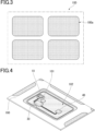
- Fig. 3 shows an example of a frame 100 for mass production.
- the frame 100 has a plurality of frame-shaped regions 100a, and an internal structure can be arranged within each frame-shaped region 100a.
- the dimensions of the frame-shaped region 100a in plan view are somewhat smaller values than the dimensions of the IC card 1 in plan view. For example, by making the frame-shaped region 100a smaller by 5 mm per side in the long side direction and the short side direction of the substantially rectangular shape in plan view, it is possible to form a substantially rectangular shape which is 10 mm smaller than the dimensions of the IC card 1 in plan view in the long side direction and the short side direction.
- Examples of materials that can be used for the frame 100 include polyvinyl chloride (PVC), polyethylene terephthalate copolymer (PET-G), and polyethylene terephthalate (PET).
- PVC polyvinyl chloride
- PET-G polyethylene terephthalate copolymer
- PET polyethylene terephthalate
- the thickness of the frame 100 is equal to or greater than the height of the tallest member of the internal structure that is not exposed on the surface of the IC card 1 except for the terminal 10, and is less than the height of the terminal 10.
- the thickness is about 450 ⁇ m.
- an auxiliary resin frame 101 is arranged to surround the terminal 10. Because the shape of the inside of the auxiliary resin frame 101 in plan view is approximately the same as that of the terminal 10, and the size of the auxiliary resin frame 101 is approximately the same as that of the terminal 10, the auxiliary resin frame 101 is slightly larger than the terminal 10. The width of the auxiliary resin frame 101 in plan view is, for example, 5 mm.
- a liquid synthetic resin is poured into the space between the frame 100 and the auxiliary resin frame 101, and covered with a surface-treated plastic film that is easily detachable to apply a pressure that uniformly spreads the resin poured inside.
- the synthetic resin is cured, the cured resin is arranged between the frame 100 and the auxiliary resin frame 101 up to approximately the same height as the frame 100 and the auxiliary resin frame 101, and a cured resin layer is formed that seals each component of the internal structure such as the IC module 30 and the memory IC 50.
- Suitable liquid synthetic resins include ultraviolet curable resins and two-liquid type curable resins.
- an ultraviolet curable resin When an ultraviolet curable resin is used, it is covered with a transparent plastic film, and after the ultraviolet curable resin is uniformly spread, ultraviolet light is irradiated through the plastic film.
- a hole may be provided in the plastic film so that excess resin can escape through the hole.
- the transmission of ultrasonic waves is adversely affected by the presence of air bubbles in the cured resin layer positioned above the sensor unit 41, it is preferable to form the cured resin layer to avoid air bubbles.
- Other methods for eliminating air bubbles above the sensor unit 41 include a method that makes the fingerprint sensor module 40 the tallest component among the components of the internal structure. As a result of the fingerprint sensor module 40 being the tallest component and having the same thickness as the frame, the cured resin is arranged around the fingerprint sensor module 40 but not above the fingerprint sensor module 40.
- one of the components of the internal structure may have the same height as the fingerprint sensor module 40. Moreover, when it is difficult to make only the fingerprint sensor module 40 the tallest component, the height may be increased by interposing an auxiliary substrate such as an interposer.
- the plastic film is detached after curing the liquid resin.
- Fig. 4 shows the state after the plastic film is detached.
- the cured resin layer 102 formed between the frame 100 and the auxiliary resin frame 101 covers each component of the internal structure which includes the fingerprint sensor module 40. Because the upper surface of the terminal 10 is arranged at a higher position than the cured resin layer 102, it is not covered with the cured resin layer 102 and maintains an exposed state.
- the frame 100 and FPC are sandwiched between two plastic sheets 105 and 106 from above and below.
- the plastic sheets 105 and 106 each have an adhesive agent applied to the surface facing the frame 100 and the FPC, and the upper plastic sheet 105 has a hole 105a at a position corresponding to the terminal 10, which has the same shape as the terminal 10 in plan view, and has the same size as the terminal 10 in plan view.
- the primary lamination is performed by applying heat and pressure to the plastic sheets 105 and 106 attached to the frame 100 and FPC.
- the surface of the lower plastic sheet 106 facing the FPC is deformed according to the unevenness of patterns such as the loop antenna and the wiring formed on the FPC, but the deformation is absorbed by the thickness of the plastic sheet 106 and the surface of the plastic sheet 106 facing away from the FPC has substantially no unevenness.
- the two plastic sheets 105 and 106 are sandwiched by two exterior plastic sheets (not illustrated) from above and below.
- the exterior plastic sheet on the upper side like the plastic sheet 105, has a hole for the terminal, and the display 20 is provided by printing at a position corresponding to the fingerprint sensor module 40 on the surface facing the plastic sheet 105.
- the IC cards 1 are completed by detaching them one at a time while being shaped.
- the materials of the plastic sheets 105 and 106 and the exterior plastic sheets include PVC, PET-G, and PET which are the materials exemplified as the material of the frame.
- the materials of the frame 100, the auxiliary resin frame 101, the plastic sheets 105 and 106, and the exterior plastic sheets are the same material, the primary and secondary laminations will fuse them together to form one piece.
- the materials of the frame 100, the auxiliary resin frame 101, the plastic sheets 105 and 106, and the external plastic sheet are the same material.
- the resin at the outer surface that covers the sensor unit 41 is preferably a single layer from the viewpoint of transmission of ultrasonic waves, it is also preferable from this viewpoint for the plastic sheets 105 and 106 and the exterior plastic sheets to be made of the same material.
- the manufacturing method described above can also be executed in a case where the fingerprint sensor module 40 is slightly taller than the frame 100.
- the plastic sheet 105 or the exterior plastic sheet on the upper side may be provided with a concave portion that does not penetrate through the sheet, at a position corresponding to the fingerprint sensor module.
- the projection of the fingerprint sensor module can be absorbed by an amount corresponding to the depth of the concave portion.
- a fingerprint of the user is registered as an initial setting at the start of use.
- the sensor unit which has been wirelessly powered by an operation from an external device or the like, operates and reads the fingerprint.
- the fingerprint that has been read is saved in the storage area of the memory IC 50.
- the user touches the position of the display 20 with the pad of the finger.
- the IC module 30 receives and matches the fingerprint data read by the sensor unit with the data for matching saved in the memory IC 50, and allows various operations such as communication only when the data are matched. This will prevent spoofing by a third party other than the user using an IC card 1.
- the fingerprint sensor module 40 including the ultrasonic fingerprint sensor (sensor unit 41) is provided, personal authentication using a fingerprint can be suitably performed, and the security is enhanced. Because ultrasonic waves pass through foreign substances attached to the finger, such as sweat and water, unlike a capacitive fingerprint sensor, the fingerprint can be stably read regardless of the humidity, the condition of the finger, and the like.
- the fingerprint can be read without any problem even if the fingerprint sensor module 40 is covered with a plastic sheet constituting the outer surface. Therefore, it is not necessary to provide a through hole in the plastic sheet for exposing the sensor unit 41, or to accurately align the through hole, and the manufacturing process can be significantly simplified compared to a case where a capacitive fingerprint sensor is used. In addition, because the plastic sheet does not need to be transparent, the degree of freedom in designing the appearance of the IC card is greatly improved.
- a frame is arranged on the FPC on which the internal structure is mounted, and a liquid resin is filled and then cured inside the frame-shaped region, which enables the resin layer that constitutes the outer surface of the IC card 1 to be formed by primary lamination and secondary lamination, while also protecting the internal structure with the cured resin layer 102.
- auxiliary resin frame 101 is arranged around the terminal 10, when the liquid synthetic resin is poured in, it is possible to suitably prevent the synthetic resin from attaching to the top surface of the terminal.
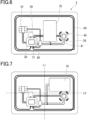
- Fig. 6 is a transparent view showing the internal structure of an IC card 2 according to the present embodiment.
- the IC card 2 further includes a rechargeable battery (power storage unit) 70 and a charging IC 80, in addition to the internal structure described in the first embodiment.
- a rechargeable battery (power storage unit) 70 and a charging IC 80, in addition to the internal structure described in the first embodiment.
- a lithium ion battery is an example of the rechargeable battery 70.
- lithium ion batteries with a thickness of about 400 ⁇ m are known, and the standard can be satisfied without any problem when such a lithium ion battery is arranged inside the IC card.
- the charging IC 80 includes an IC chip, and is connected to the rechargeable battery 70.
- the charging IC 80 selects the charging input, and controls the charging by switching it on or off.
- the charging IC 80 is connected to the terminal 10 and the loop antenna 60.
- the IC card 2 handles inputs from two systems, namely input from the terminal 10 and input from the loop antenna 60, and although it is configured to be chargeable from either system, this is not essential and a configuration is possible that handles input from either one of the systems.
- the input from the terminal 10 has an advantage that charging can be performed efficiently, and the input from the loop antenna 60 has an advantage that the charging can be performed without the need for a special device when away from home.
- the IC card 2 of the present embodiment provides the same effects as the IC card 1 according to the first embodiment.
- the fingerprint sensor module 40 can be stably operated. That is, although an ultrasonic fingerprint sensor has a greater power consumption than a capacitive fingerprint sensor, even when the wireless power supply from the loop antenna 60 is not sufficient, by supplying power to the fingerprint sensor module 40 from the rechargeable battery 70, it is possible to perform acquisition, matching, and authentication processing, registration processing, and the like, of the fingerprint data without being restricted by the location or environment.
- an electric double layer capacitor may be used as the power storage unit. In this configuration, the charging IC 80 becomes unnecessary.
- the thickness of the power storage unit is preferably 400 ⁇ m or less from the viewpoint of satisfying the standard mentioned above.
- the above standard can be satisfied by providing a through hole in the FPC and arranging the power storage unit inside the through hole.
- the area of the power storage unit in plan view is preferably 600 mm 2 or less.
- the power storage unit can be easily arranged with the other components of the internal structure inside a loop antenna that conforms to the card dimension standard.
- the power storage unit is, like the rechargeable battery 70 shown in Fig. 7 , preferably arranged at a position away from the center line L 1 in the long side direction and the away from the center line L2 in the short side direction in plan view of the IC card. As a result, the bending resistance of the IC card can be improved.
- the IC module 30 may be configured such that registration or rewriting of the fingerprint is allowed only when power of a certain value or more is being supplied from the loop antenna 60, or when power is being supplied from the terminal 10. Because the power consumption of the fingerprint sensor module 40 is a maximum during the fingerprint data registration process, such a configuration enables the operation of the IC card 2 to be stabilized.
- the IC chip included in the IC module does not have to be arranged in the form of a module.
- the IC chip may be arranged alone in an internal circuit.
- the IC card according to the present invention does not have to be a dual IC card. Therefore, the configuration may be such that only one of contact communication and contactless communication is possible.
- the terminal 10 is not necessary in a configuration where only contactless communication is possible, the terminal 10 may be provided only for charging in a configuration where the power storage unit is included.
- the memory IC which is a storage unit
- the memory IC may be omitted by providing the IC module with the function of the storage unit.
- part of the internal structure may be mounted on the surface on the opposite side of the FPC such that the internal structure is mounted on both sides of the FPC.
- the fingerprint sensor module may be mounted on the surface on the opposite side of the FPC.
- a frame may be arranged on the surface on the other side of the FPC to form a cured resin layer.
- the IC card according to the present invention may include a display that is capable of various displays. Alternatively, one or more LEDs (light-emitting diodes) may be provided. In these modes, various types of information (completion of registration of fingerprint data, result of fingerprint authentication, and the like) can be shown on the display, or by the light emission mode of the LED.
- LEDs light-emitting diodes
- the display or the light-emitting diodes may be exposed through a hole formed in the plastic outer surface, and it is also possible to have a configuration in which the display or light emission is visible without exposure by having part of the outer surface to be transparent.
- the display that indicates the position of the fingerprint sensor is not limited to printing represented by the display 20, and may be configured by unevenness in the plastic constituting the outer surface of the IC card. However, in this case, it should have a configuration in which the thickness and flatness do not affect reading of the fingerprint, and should be arranged to not overlap with the sensor unit 41 in plan view.
- a switch may be arranged in or around the fingerprint reading area. In this case, the power consumption of the IC card can be suppressed by operating the fingerprint sensor only when the switch is on.
- a suitable switch can be, for example, a capacitive touch sensor that is operated by power obtained by the loop antenna, or is controlled to be operated at the same time as the start of contactless communication.
- a capacitive touch sensor can be, for example, a capacitive touch sensor that is operated by power obtained by the loop antenna, or is controlled to be operated at the same time as the start of contactless communication.
- the IC card and the method for manufacturing an IC card of the present invention have a configuration in which security is enhanced without restricting the design.
Landscapes
- Engineering & Computer Science (AREA)
- Computer Hardware Design (AREA)
- Microelectronics & Electronic Packaging (AREA)
- Physics & Mathematics (AREA)
- General Physics & Mathematics (AREA)
- Theoretical Computer Science (AREA)
- Computer Security & Cryptography (AREA)
- General Engineering & Computer Science (AREA)
- Automation & Control Theory (AREA)
- Credit Cards Or The Like (AREA)
Abstract
Description
- The present invention relates to an IC card, and more specifically an IC card provided with a fingerprint sensor, and a method for manufacturing the IC card.
- The present application claims the benefit of priority from
Japanese Patent Application No. 2020-177186 filed in Japan on October 22, 2020 - IC cards are widely known as a contact communication medium and a contactless communication medium (for example, see PTL 1).
- PTL 1:
WO 99/26195 - As IC cards provided with enhanced security, IC cards equipped with a capacitive fingerprint sensor are known. Because a capacitive fingerprint sensor requires a finger to directly contact a detection surface, the fingerprint sensor needs to be exposed on the surface of the card. Therefore, it is necessary to open a hole in the base material of the card, and to precisely align the fingerprint sensor and the hole, which makes the manufacturing process complicated. Further, the holes also constrain the design of the card.
- In view of the above circumstances, an object of the present invention is to provide an IC card and a method for manufacturing an IC card having a configuration that enhances security without restricting the design.
- A first aspect of the present invention is an IC card including an IC chip and configured to enable at least one of contact communication and contactless communication.
- The IC card includes an ultrasonic fingerprint sensor connected to the IC chip, and a storage unit in which fingerprint data for matching is stored.
- An outer surface of the IC card is formed of synthetic resin, and the ultrasonic fingerprint sensor is covered with the synthetic resin.
- A second aspect of the present invention is a method for manufacturing the IC card according to the first aspect.
- The manufacturing method includes: mounting the IC chip, the ultrasonic fingerprint sensor, and the storage unit on a flexible substrate; arranging a frame made of resin on the flexible substrate to surround the IC chip, the ultrasonic fingerprint sensor, and the storage unit; and forming a cured resin layer that seals the IC chip and the storage unit by filling and curing the synthetic resin inside a space surrounded by the frame.
- The IC card and the method for manufacturing an IC card of the present invention have a configuration in which security is enhanced without restricting the design.
-
-
Fig. 1 is a schematic plan view of an IC card according to a first embodiment of the present invention. -
Fig. 2 is a transparent view showing the internal structure of the IC card inFig. 1 . -
Fig. 3 is a diagram showing an example of a frame used for manufacturing the IC card inFig. 1 . -
Fig. 4 is a diagram showing a process performed while manufacturing the IC card inFig. 1 . -
Fig. 5 is a diagram showing a process performed while manufacturing the IC card inFig. 1 . -
Fig. 6 is a transparent view showing an internal structure of an IC card according to a second embodiment of the present invention. -
Fig. 7 is a transparent view showing the internal structure of a modification of the IC card inFig. 6 . - A first embodiment of the present invention will be described below with reference to
Figs. 1 to 5 . -
Fig. 1 is a schematic plan view of anIC card 1 according to the present embodiment. As shown inFig. 1 , theIC card 1 includes aterminal 10 and adisplay 20 on the upper surface of theIC card 1. Theterminal 10 is for contact communication, and is exposed on the outer surface of theIC card 1. Thedisplay 20 indicates the position of a fingerprint sensor, and is provided on the outer surface of theIC card 1. - The
terminal 10 has a known configuration, for example, in which a copper pattern is formed on both sides of a base material made of glass epoxy, polyimide, or the like. The copper pattern is subjected to a plating process with nickel, palladium, gold, or the like. - The outer surface of the
IC card 1 is made of synthetic resin. Such a configuration can be realized, for example, by sandwiching an internal structure that includes an IC module, a fingerprint sensor, and the like, between an upper resin substrate and a lower resin substrate, and then joining the upper resin substrate and the lower resin substrate by adhesion, heating, or the like. The details of the manufacturing procedure of theIC card 1 will be described later. -
Fig. 2 is a transparent view showing the internal structure of theIC card 1 in the same posture asFig. 1 . TheIC card 1 includes anIC module 30, afingerprint sensor module 40, amemory IC 50, and aloop antenna 60. - The
IC module 30 includes anIC chip 31. TheIC module 30 performs communication between theIC card 1 and an external device, matching and authentication of a fingerprint detected by thefingerprint sensor module 40, and the like. TheIC module 30 is connected to each of theterminal 10, thefingerprint sensor module 40, thememory IC 50, and theloop antenna 60. - The
fingerprint sensor module 40 includes asensor unit 41 that reads a fingerprint, and an IC chip that controls the operation of thesensor unit 41, and is connected to the IC module 30 (IC chip 31). - A known ultrasonic fingerprint sensor is used as the
sensor unit 41. Since the ultrasonic waves emitted by an ultrasonic fingerprint sensor can pass through exterior members such as glass and plastic, a fingerprint can be read without touching thesensor unit 41. Therefore, it is not necessary to expose thesensor unit 41 on the surface of theIC card 1, and the user can recognize the position of thesensor unit 41 provided that thedisplay 20 is present. - The
memory IC 50 includes a storage area and an IC chip, and is connected to theIC module 30. The storage area can store one or more fingerprint data for matching, and provides the stored fingerprint data to theIC module 30 in response to a request from theIC module 30. - The
loop antenna 60 has a configuration in which a conductor is formed in a loop shape, and is connected to theIC module 30. Theloop antenna 60 is formed by appropriately using jumper wires, vias, or the like so that the wires do not touch each other. - The
IC card 1 is configured as a dual IC card that can perform both contact communication and contactless communication by providing theloop antenna 60. Furthermore, power can be supplied to thefingerprint sensor module 40 by wireless power supply from an external device via theloop antenna 60. - An example of a manufacturing procedure of the
IC card 1 configured as described above will be described. - First, a flexible substrate (FPC) for mounting the internal structure is prepared. The configuration of the FPC is known, and includes, for example, a conductor layer that forms a circuit pattern on both sides of a base material made of polyimide with a thickness of about 50 µm. For example, the thickness of the conductor layer including the plated layer can be 25 µm, for example.
- Next, the conductor layer of the FPC is patterned to form the
loop antenna 60 and the wiring that connects each component of the internal structure, and then the internal structure, such as theterminal 10, theIC module 30, thefingerprint sensor module 40, and the memory IC, is mounted on the FPC. Examples of the mounting method include solder surface mounting (SMT), and thermocompression bonding using an anisotropic conductive film (ACF) or an anisotropic conductive paste (ACP). A large number ofIC cards 1 can be manufactured by forming a plurality of sets of internal structures on a large-area FPC. - Then, a plastic (resin) frame is arranged from above the internal structure, and the frame and the FPC are bonded together so that the entire internal structure, including the
loop antenna 60, is surrounded by the frame. An adhesive agent may be applied to the frame in advance. -
Fig. 3 shows an example of aframe 100 for mass production. Theframe 100 has a plurality of frame-shapedregions 100a, and an internal structure can be arranged within each frame-shapedregion 100a. The dimensions of the frame-shapedregion 100a in plan view are somewhat smaller values than the dimensions of theIC card 1 in plan view. For example, by making the frame-shapedregion 100a smaller by 5 mm per side in the long side direction and the short side direction of the substantially rectangular shape in plan view, it is possible to form a substantially rectangular shape which is 10 mm smaller than the dimensions of theIC card 1 in plan view in the long side direction and the short side direction. - Examples of materials that can be used for the
frame 100 include polyvinyl chloride (PVC), polyethylene terephthalate copolymer (PET-G), and polyethylene terephthalate (PET). - As a general rule, the thickness of the
frame 100 is equal to or greater than the height of the tallest member of the internal structure that is not exposed on the surface of theIC card 1 except for the terminal 10, and is less than the height of the terminal 10. When expressed numerically, for example, the thickness is about 450 µm. - Further, as shown in
Fig. 4 , anauxiliary resin frame 101 is arranged to surround the terminal 10. Because the shape of the inside of theauxiliary resin frame 101 in plan view is approximately the same as that of the terminal 10, and the size of theauxiliary resin frame 101 is approximately the same as that of the terminal 10, theauxiliary resin frame 101 is slightly larger than the terminal 10. The width of theauxiliary resin frame 101 in plan view is, for example, 5 mm. - Next, a liquid synthetic resin is poured into the space between the
frame 100 and theauxiliary resin frame 101, and covered with a surface-treated plastic film that is easily detachable to apply a pressure that uniformly spreads the resin poured inside. Then, when the synthetic resin is cured, the cured resin is arranged between theframe 100 and theauxiliary resin frame 101 up to approximately the same height as theframe 100 and theauxiliary resin frame 101, and a cured resin layer is formed that seals each component of the internal structure such as theIC module 30 and thememory IC 50. - Suitable liquid synthetic resins include ultraviolet curable resins and two-liquid type curable resins. When an ultraviolet curable resin is used, it is covered with a transparent plastic film, and after the ultraviolet curable resin is uniformly spread, ultraviolet light is irradiated through the plastic film.
- In the step described above, a hole may be provided in the plastic film so that excess resin can escape through the hole.
- Furthermore, because the transmission of ultrasonic waves is adversely affected by the presence of air bubbles in the cured resin layer positioned above the
sensor unit 41, it is preferable to form the cured resin layer to avoid air bubbles. - Other methods for eliminating air bubbles above the
sensor unit 41 include a method that makes thefingerprint sensor module 40 the tallest component among the components of the internal structure. As a result of thefingerprint sensor module 40 being the tallest component and having the same thickness as the frame, the cured resin is arranged around thefingerprint sensor module 40 but not above thefingerprint sensor module 40. - When this method is adopted, one of the components of the internal structure may have the same height as the
fingerprint sensor module 40. Moreover, when it is difficult to make only thefingerprint sensor module 40 the tallest component, the height may be increased by interposing an auxiliary substrate such as an interposer. - The plastic film is detached after curing the liquid resin.
-
Fig. 4 shows the state after the plastic film is detached. The curedresin layer 102 formed between theframe 100 and theauxiliary resin frame 101 covers each component of the internal structure which includes thefingerprint sensor module 40. Because the upper surface of the terminal 10 is arranged at a higher position than the curedresin layer 102, it is not covered with the curedresin layer 102 and maintains an exposed state. - Next, as shown in
Fig. 5 , theframe 100 and FPC are sandwiched between twoplastic sheets plastic sheets frame 100 and the FPC, and theupper plastic sheet 105 has ahole 105a at a position corresponding to the terminal 10, which has the same shape as the terminal 10 in plan view, and has the same size as the terminal 10 in plan view. - Then, the primary lamination is performed by applying heat and pressure to the
plastic sheets frame 100 and FPC. As a result of primary lamination, the surface of the lowerplastic sheet 106 facing the FPC is deformed according to the unevenness of patterns such as the loop antenna and the wiring formed on the FPC, but the deformation is absorbed by the thickness of theplastic sheet 106 and the surface of theplastic sheet 106 facing away from the FPC has substantially no unevenness. - Finally, the two
plastic sheets plastic sheet 105, has a hole for the terminal, and thedisplay 20 is provided by printing at a position corresponding to thefingerprint sensor module 40 on the surface facing theplastic sheet 105. - After the secondary lamination is performed by applying heat and pressure to the attached exterior plastic sheets, the
IC cards 1 are completed by detaching them one at a time while being shaped. - Examples of the materials of the
plastic sheets frame 100, theauxiliary resin frame 101, theplastic sheets frame 100, theauxiliary resin frame 101, theplastic sheets sensor unit 41 is preferably a single layer from the viewpoint of transmission of ultrasonic waves, it is also preferable from this viewpoint for theplastic sheets - Moreover, the manufacturing method described above can also be executed in a case where the
fingerprint sensor module 40 is slightly taller than theframe 100. In this case, theplastic sheet 105 or the exterior plastic sheet on the upper side may be provided with a concave portion that does not penetrate through the sheet, at a position corresponding to the fingerprint sensor module. As a result, the projection of the fingerprint sensor module can be absorbed by an amount corresponding to the depth of the concave portion. - The operations performed when using the
IC card 1 configured as described above will be described. - A fingerprint of the user is registered as an initial setting at the start of use. In a state where the user is touching the position of the
display 20 with the pad of the finger, the sensor unit, which has been wirelessly powered by an operation from an external device or the like, operates and reads the fingerprint. The fingerprint that has been read is saved in the storage area of thememory IC 50. - When confirming the identity of the user, the user touches the position of the
display 20 with the pad of the finger. TheIC module 30 receives and matches the fingerprint data read by the sensor unit with the data for matching saved in thememory IC 50, and allows various operations such as communication only when the data are matched. This will prevent spoofing by a third party other than the user using anIC card 1. - As described above, according to the
IC card 1 of the present embodiment, because thefingerprint sensor module 40 including the ultrasonic fingerprint sensor (sensor unit 41) is provided, personal authentication using a fingerprint can be suitably performed, and the security is enhanced. Because ultrasonic waves pass through foreign substances attached to the finger, such as sweat and water, unlike a capacitive fingerprint sensor, the fingerprint can be stably read regardless of the humidity, the condition of the finger, and the like. - In addition, because ultrasonic waves pass through the skin to a certain depth, it is also possible to sense blood flow, and three-dimensionally detect ridges and sweat pores in the fingerprint. As a result of appropriately combining these, it is also possible to improve the fingerprint matching accuracy.
- Furthermore, because ultrasonic waves pass through plastic, the fingerprint can be read without any problem even if the
fingerprint sensor module 40 is covered with a plastic sheet constituting the outer surface. Therefore, it is not necessary to provide a through hole in the plastic sheet for exposing thesensor unit 41, or to accurately align the through hole, and the manufacturing process can be significantly simplified compared to a case where a capacitive fingerprint sensor is used. In addition, because the plastic sheet does not need to be transparent, the degree of freedom in designing the appearance of the IC card is greatly improved. - According to the method for manufacturing the
IC card 1 described above, a frame is arranged on the FPC on which the internal structure is mounted, and a liquid resin is filled and then cured inside the frame-shaped region, which enables the resin layer that constitutes the outer surface of theIC card 1 to be formed by primary lamination and secondary lamination, while also protecting the internal structure with the curedresin layer 102. - Moreover, because the
auxiliary resin frame 101 is arranged around the terminal 10, when the liquid synthetic resin is poured in, it is possible to suitably prevent the synthetic resin from attaching to the top surface of the terminal. - A second embodiment of the present invention will be described with reference to
Figs. 6 and 7 . In the following description, those configurations that are common to the members already described are given the same reference signs, and duplicate descriptions are omitted. -
Fig. 6 is a transparent view showing the internal structure of anIC card 2 according to the present embodiment. TheIC card 2 further includes a rechargeable battery (power storage unit) 70 and a chargingIC 80, in addition to the internal structure described in the first embodiment. - A lithium ion battery is an example of the
rechargeable battery 70. Although standards have been established that relate to the thickness range of an IC card to which the present invention is applied, lithium ion batteries with a thickness of about 400 µm are known, and the standard can be satisfied without any problem when such a lithium ion battery is arranged inside the IC card. - The charging
IC 80 includes an IC chip, and is connected to therechargeable battery 70. The chargingIC 80 selects the charging input, and controls the charging by switching it on or off. In the present embodiment, the chargingIC 80 is connected to the terminal 10 and theloop antenna 60. As a result, theIC card 2 handles inputs from two systems, namely input from the terminal 10 and input from theloop antenna 60, and although it is configured to be chargeable from either system, this is not essential and a configuration is possible that handles input from either one of the systems. The input from the terminal 10 has an advantage that charging can be performed efficiently, and the input from theloop antenna 60 has an advantage that the charging can be performed without the need for a special device when away from home. - The
IC card 2 of the present embodiment provides the same effects as theIC card 1 according to the first embodiment. - Furthermore, because the
rechargeable battery 70 is provided as a power storage unit, thefingerprint sensor module 40 can be stably operated. That is, although an ultrasonic fingerprint sensor has a greater power consumption than a capacitive fingerprint sensor, even when the wireless power supply from theloop antenna 60 is not sufficient, by supplying power to thefingerprint sensor module 40 from therechargeable battery 70, it is possible to perform acquisition, matching, and authentication processing, registration processing, and the like, of the fingerprint data without being restricted by the location or environment. - In the present embodiment, an electric double layer capacitor may be used as the power storage unit. In this configuration, the charging
IC 80 becomes unnecessary. - In either configuration, the thickness of the power storage unit is preferably 400 µm or less from the viewpoint of satisfying the standard mentioned above. However, as long as the thickness of the power storage unit is 450 µm or less, the above standard can be satisfied by providing a through hole in the FPC and arranging the power storage unit inside the through hole.
- The area of the power storage unit in plan view is preferably 600 mm2 or less. For example, in the case of a 20 mm × 30 mm rectangular shape that satisfies the above, the power storage unit can be easily arranged with the other components of the internal structure inside a loop antenna that conforms to the card dimension standard. The power storage unit is, like the
rechargeable battery 70 shown inFig. 7 , preferably arranged at a position away from thecenter line L 1 in the long side direction and the away from the center line L2 in the short side direction in plan view of the IC card. As a result, the bending resistance of the IC card can be improved. - In the present embodiment, the
IC module 30 may be configured such that registration or rewriting of the fingerprint is allowed only when power of a certain value or more is being supplied from theloop antenna 60, or when power is being supplied from the terminal 10. Because the power consumption of thefingerprint sensor module 40 is a maximum during the fingerprint data registration process, such a configuration enables the operation of theIC card 2 to be stabilized. - Although the embodiments of the present invention have been described in detail with reference to the accompanying drawings, specific configurations are not limited to the embodiments, which can be modified and combined within a scope not departing from the spirit of the present invention. Some of the modifications are described below. These can be appropriately combined.
- In the IC card according to the present invention, the IC chip included in the IC module does not have to be arranged in the form of a module. For example, the IC chip may be arranged alone in an internal circuit.
- The IC card according to the present invention does not have to be a dual IC card. Therefore, the configuration may be such that only one of contact communication and contactless communication is possible. Although the terminal 10 is not necessary in a configuration where only contactless communication is possible, the terminal 10 may be provided only for charging in a configuration where the power storage unit is included.
- In the above description, although an example has been described in which the memory IC, which is a storage unit, is configured separately from the IC module, the memory IC may be omitted by providing the IC module with the function of the storage unit.
- In the above description, although an example has been described in which the entire internal structure is mounted on one surface of the FPC, part of the internal structure may be mounted on the surface on the opposite side of the FPC such that the internal structure is mounted on both sides of the FPC. For example, only the fingerprint sensor module may be mounted on the surface on the opposite side of the FPC. In this case, after a frame is arranged on the surface on one side of the FPC to form a cured resin layer, a frame may be arranged on the surface on the other side of the FPC to form a cured resin layer.
- The IC card according to the present invention may include a display that is capable of various displays. Alternatively, one or more LEDs (light-emitting diodes) may be provided. In these modes, various types of information (completion of registration of fingerprint data, result of fingerprint authentication, and the like) can be shown on the display, or by the light emission mode of the LED.
- The display or the light-emitting diodes may be exposed through a hole formed in the plastic outer surface, and it is also possible to have a configuration in which the display or light emission is visible without exposure by having part of the outer surface to be transparent.
- The display that indicates the position of the fingerprint sensor is not limited to printing represented by the
display 20, and may be configured by unevenness in the plastic constituting the outer surface of the IC card. However, in this case, it should have a configuration in which the thickness and flatness do not affect reading of the fingerprint, and should be arranged to not overlap with thesensor unit 41 in plan view. - In the IC card, a switch may be arranged in or around the fingerprint reading area. In this case, the power consumption of the IC card can be suppressed by operating the fingerprint sensor only when the switch is on.
- A suitable switch can be, for example, a capacitive touch sensor that is operated by power obtained by the loop antenna, or is controlled to be operated at the same time as the start of contactless communication. As a result of arranging a capacitive touch sensor over the sensor unit of the fingerprint sensor, the user can turn on the power of the fingerprint sensor or release the fingerprint sensor from a sleep mode with the natural action of touching the location indicated by the display. Because a capacitive touch sensor can detect a finger that is making contact through plastic, even in this configuration, effects such as the simplification of the manufacturing process and improvement in the degree of freedom of designing the appearance are not lost.
- The IC card and the method for manufacturing an IC card of the present invention have a configuration in which security is enhanced without restricting the design.
-
- 1, 2 IC card
- 10 Terminal
- 20 Display
- 30 IC module
- 40 Fingerprint sensor module
- 50 Memory IC (storage unit)
- 60 Loop antenna
- 70 Rechargeable battery (power storage unit)
- 100 Frame
- 102 Cured resin layer
Claims (6)
- An IC card provided with an IC chip, and configured to enable at least one of contact communication and contactless communication, the IC chip comprising:an ultrasonic fingerprint sensor connected to the IC chip; anda storage unit in which fingerprint data for matching is stored; whereinan outer surface of the IC card is formed of synthetic resin, andthe ultrasonic fingerprint sensor is covered with the synthetic resin.
- The IC card according to claim 1, further comprisinga terminal connected to the IC chip and exposed on the outer surface, whereinthe IC card is configured to enable contact communication.
- The IC card according to claim 1, further comprisinga loop antenna connected to the IC chip, whereinthe IC card is configured to enable contactless communication.
- The IC card according to claim 1, further comprising
a power storage unit that supplies power to the ultrasonic fingerprint sensor. - The IC card according to claim 1, wherein
the outer surface is provided with a display that indicates a position of the ultrasonic fingerprint sensor. - A method for manufacturing the IC card according to claim 1, comprising:mounting the IC chip, the ultrasonic fingerprint sensor, and the storage unit on a flexible substrate;arranging a frame made of resin on the flexible substrate to surround the IC chip, the ultrasonic fingerprint sensor, and the storage unit; andforming a cured resin layer that seals the IC chip and the storage unit by filling and curing the synthetic resin inside a space surrounded by the frame.
Applications Claiming Priority (2)
| Application Number | Priority Date | Filing Date | Title |
|---|---|---|---|
| JP2020177186 | 2020-10-22 | ||
| PCT/JP2021/035566 WO2022085376A1 (en) | 2020-10-22 | 2021-09-28 | Ic card and method for manufacturing ic card |
Publications (3)
| Publication Number | Publication Date |
|---|---|
| EP4235499A1 true EP4235499A1 (en) | 2023-08-30 |
| EP4235499A4 EP4235499A4 (en) | 2024-04-24 |
| EP4235499B1 EP4235499B1 (en) | 2026-04-29 |
Family
ID=81289873
Family Applications (1)
| Application Number | Title | Priority Date | Filing Date |
|---|---|---|---|
| EP21882517.2A Active EP4235499B1 (en) | 2020-10-22 | 2021-09-28 | Ic card and method for manufacturing ic card |
Country Status (5)
| Country | Link |
|---|---|
| US (1) | US12217112B2 (en) |
| EP (1) | EP4235499B1 (en) |
| JP (1) | JPWO2022085376A1 (en) |
| CN (1) | CN116018597A (en) |
| WO (1) | WO2022085376A1 (en) |
Families Citing this family (4)
| Publication number | Priority date | Publication date | Assignee | Title |
|---|---|---|---|---|
| GB2577477B8 (en) * | 2018-08-31 | 2022-02-16 | Idex Biometrics Asa | Biometric Interface |
| TWI856170B (en) * | 2019-10-25 | 2024-09-21 | 美商坎柏斯庫爾有限責任公司 | Metal card with biometric features |
| DE102021112447B4 (en) * | 2021-05-12 | 2024-06-20 | Infineon Technologies Ag | Chip card biometric sensor component, chip card, method for forming a chip card biometric sensor component and method for forming a chip card |
| US12106308B2 (en) * | 2022-07-08 | 2024-10-01 | Bank Of America Corporation | Auxiliary battery power authentication system for use with an EMV contactless secure transaction card |
Family Cites Families (19)
| Publication number | Priority date | Publication date | Assignee | Title |
|---|---|---|---|---|
| CN1179295C (en) | 1997-11-14 | 2004-12-08 | 凸版印刷株式会社 | Composite IC module and composite IC card |
| CA2601512A1 (en) * | 2005-03-23 | 2006-09-28 | Cardxx, Inc. | Method for making advanced smart cards with integrated electronics using isotropic thermoset adhesive materials with high quality exterior surfaces |
| KR101168056B1 (en) * | 2010-09-30 | 2012-07-24 | 권성규 | Smart electronic card |
| WO2014208437A1 (en) * | 2013-06-25 | 2014-12-31 | 凸版印刷株式会社 | Dual ic card |
| WO2016073202A1 (en) * | 2014-11-04 | 2016-05-12 | Intelligent Technologies International, Inc. | Smartcard |
| KR20160138917A (en) * | 2015-05-26 | 2016-12-06 | 크루셜텍 (주) | Smart card comprising fingerprint detecting device and method for driving the same |
| CN107615296A (en) * | 2016-04-21 | 2018-01-19 | 华为技术有限公司 | A kind of hand-hold electronic equipments |
| CN107346443A (en) * | 2016-05-05 | 2017-11-14 | 魏赛琦 | A kind of one-piece type smart card and preparation method thereof |
| US10846501B2 (en) | 2017-04-28 | 2020-11-24 | The Board Of Trustees Of The Leland Stanford Junior University | Acoustic biometric touch scanner |
| WO2018221429A1 (en) * | 2017-06-02 | 2018-12-06 | パナソニックIpマネジメント株式会社 | Security system comprising biometric authentication sensor, and electronic device |
| FR3069082B1 (en) * | 2017-07-17 | 2019-08-16 | Idemia Identity And Security | ELECTRONIC CARD COMPRISING AN IMPRESSION SENSOR AND A TOUCHABLE MARK |
| CN207489033U (en) * | 2017-07-18 | 2018-06-12 | 深圳市云传智联技术有限公司 | A kind of payment system and bank card based on fingerprint identification technology |
| CN207764884U (en) * | 2018-01-29 | 2018-08-24 | 南昌欧菲生物识别技术有限公司 | card device |
| JP7123710B2 (en) * | 2018-09-18 | 2022-08-23 | 株式会社東芝 | IC cards and portable electronic devices |
| JP7273474B2 (en) * | 2018-09-19 | 2023-05-15 | 株式会社東芝 | IC cards and portable electronic devices |
| JP2020107101A (en) * | 2018-12-27 | 2020-07-09 | 株式会社東芝 | IC card and portable electronic device |
| US10929636B2 (en) * | 2019-01-18 | 2021-02-23 | Qualcomm Incorporated | Ultrasonic fingerprint sensor with electrically nonconductive acoustic layer |
| JP6697109B1 (en) | 2019-04-22 | 2020-05-20 | 日東電工株式会社 | Method for manufacturing optical display device |
| TWI856170B (en) * | 2019-10-25 | 2024-09-21 | 美商坎柏斯庫爾有限責任公司 | Metal card with biometric features |
-
2021
- 2021-09-28 EP EP21882517.2A patent/EP4235499B1/en active Active
- 2021-09-28 WO PCT/JP2021/035566 patent/WO2022085376A1/en not_active Ceased
- 2021-09-28 JP JP2022557341A patent/JPWO2022085376A1/ja active Pending
- 2021-09-28 CN CN202180051503.XA patent/CN116018597A/en active Pending
-
2023
- 2023-04-14 US US18/134,959 patent/US12217112B2/en active Active
Also Published As
| Publication number | Publication date |
|---|---|
| EP4235499A4 (en) | 2024-04-24 |
| US20230259734A1 (en) | 2023-08-17 |
| CN116018597A (en) | 2023-04-25 |
| WO2022085376A1 (en) | 2022-04-28 |
| EP4235499B1 (en) | 2026-04-29 |
| JPWO2022085376A1 (en) | 2022-04-28 |
| US12217112B2 (en) | 2025-02-04 |
Similar Documents
| Publication | Publication Date | Title |
|---|---|---|
| EP4235499B1 (en) | Ic card and method for manufacturing ic card | |
| US9990577B2 (en) | Card with built-in electronic component | |
| CN110392894A (en) | Chip card and method for manufacturing chip card | |
| CN109271835B (en) | Electronic board with fingerprint collector and manufacturing method thereof | |
| US9633301B2 (en) | IC module, dual IC card, and method for manufacturing IC module | |
| JP2002342731A (en) | Composite IC card | |
| US11410450B2 (en) | Method for manufacturing an electronic device including multiple fixing members to fix a biometric sensor to a display | |
| EP3086208B1 (en) | Smart card with touch-based interface | |
| CN102074722A (en) | Handheld equipment battery and handheld equipment | |
| CN111989638B (en) | Electronic device including a plurality of fixing members for fixing a biosensor to a display and method for manufacturing the same | |
| US10403617B2 (en) | Fingerprint recognition module having light-emitting function and manufacturing method therefor | |
| EP3948667B1 (en) | An improved card with fingerprint biometrics | |
| US10176421B2 (en) | Method for producing a data carrier that prevents mechanical strains between chip and data carrier body | |
| US12361253B2 (en) | Data-bearing card and semi-finished product and wiring layout for same, and method for producing same | |
| WO2022157330A1 (en) | Electronic module with indication device | |
| KR101165087B1 (en) | Fingerprint recognition card equipped with stiffening plate | |
| JP2022011487A (en) | Antenna device and card which is antenna device | |
| KR20080084767A (en) | Electronic card module and its manufacturing method | |
| JP2009157743A (en) | IC non-mounted external connection terminal board type dual IC card | |
| JP5710395B2 (en) | IC card | |
| JP4085790B2 (en) | IC card manufacturing method | |
| JP4734742B2 (en) | IC module and manufacturing method thereof | |
| US20090109000A1 (en) | Rfid tag and manufacturing method thereof | |
| JP2013077237A (en) | Ic card | |
| KR101020706B1 (en) | Card type receiver and manufacturing method |
Legal Events
| Date | Code | Title | Description |
|---|---|---|---|
| STAA | Information on the status of an ep patent application or granted ep patent |
Free format text: STATUS: THE INTERNATIONAL PUBLICATION HAS BEEN MADE |
|
| PUAI | Public reference made under article 153(3) epc to a published international application that has entered the european phase |
Free format text: ORIGINAL CODE: 0009012 |
|
| STAA | Information on the status of an ep patent application or granted ep patent |
Free format text: STATUS: REQUEST FOR EXAMINATION WAS MADE |
|
| 17P | Request for examination filed |
Effective date: 20230322 |
|
| AK | Designated contracting states |
Kind code of ref document: A1 Designated state(s): AL AT BE BG CH CY CZ DE DK EE ES FI FR GB GR HR HU IE IS IT LI LT LU LV MC MK MT NL NO PL PT RO RS SE SI SK SM TR |
|
| DAV | Request for validation of the european patent (deleted) | ||
| DAX | Request for extension of the european patent (deleted) | ||
| A4 | Supplementary search report drawn up and despatched |
Effective date: 20240326 |
|
| RIC1 | Information provided on ipc code assigned before grant |
Ipc: B42D 25/46 20140101ALI20240320BHEP Ipc: B42D 25/313 20140101ALI20240320BHEP Ipc: G06K 19/077 20060101ALI20240320BHEP Ipc: G06K 19/073 20060101ALI20240320BHEP Ipc: G06K 19/07 20060101AFI20240320BHEP |
|
| STAA | Information on the status of an ep patent application or granted ep patent |
Free format text: STATUS: EXAMINATION IS IN PROGRESS |
|
| 17Q | First examination report despatched |
Effective date: 20250527 |
|
| GRAP | Despatch of communication of intention to grant a patent |
Free format text: ORIGINAL CODE: EPIDOSNIGR1 |
|
| STAA | Information on the status of an ep patent application or granted ep patent |
Free format text: STATUS: GRANT OF PATENT IS INTENDED |
|
| INTG | Intention to grant announced |
Effective date: 20260114 |
|
| RIN1 | Information on inventor provided before grant (corrected) |
Inventor name: KATANO, YUKIKO Inventor name: TSUKADA, TETSUYA Inventor name: KATAOKA, SHIN |
|
| GRAS | Grant fee paid |
Free format text: ORIGINAL CODE: EPIDOSNIGR3 |
|
| GRAA | (expected) grant |
Free format text: ORIGINAL CODE: 0009210 |
|
| STAA | Information on the status of an ep patent application or granted ep patent |
Free format text: STATUS: THE PATENT HAS BEEN GRANTED |
|
| AK | Designated contracting states |
Kind code of ref document: B1 Designated state(s): AL AT BE BG CH CY CZ DE DK EE ES FI FR GB GR HR HU IE IS IT LI LT LU LV MC MK MT NL NO PL PT RO RS SE SI SK SM TR |
|
| REG | Reference to a national code |
Ref country code: CH Ref legal event code: F10 Free format text: ST27 STATUS EVENT CODE: U-0-0-F10-F00 (AS PROVIDED BY THE NATIONAL OFFICE) Effective date: 20260429 Ref country code: GB Ref legal event code: FG4D |