EP4224219A2 - Dispositifs et compositions à base de structure photonique destinés à être utilisés dans l'imagerie luminescente de sites multiples à l'intérieur d'un pixel, et leurs procédés d'utilisation - Google Patents
Dispositifs et compositions à base de structure photonique destinés à être utilisés dans l'imagerie luminescente de sites multiples à l'intérieur d'un pixel, et leurs procédés d'utilisation Download PDFInfo
- Publication number
- EP4224219A2 EP4224219A2 EP23166545.6A EP23166545A EP4224219A2 EP 4224219 A2 EP4224219 A2 EP 4224219A2 EP 23166545 A EP23166545 A EP 23166545A EP 4224219 A2 EP4224219 A2 EP 4224219A2
- Authority
- EP
- European Patent Office
- Prior art keywords
- luminophore
- array
- feature
- photons
- features
- Prior art date
- Legal status (The legal status is an assumption and is not a legal conclusion. Google has not performed a legal analysis and makes no representation as to the accuracy of the status listed.)
- Pending
Links
- 238000003384 imaging method Methods 0.000 title claims abstract description 125
- 238000000034 method Methods 0.000 title claims description 111
- 239000000203 mixture Substances 0.000 title description 32
- 230000010287 polarization Effects 0.000 claims abstract description 134
- 102000039446 nucleic acids Human genes 0.000 claims description 101
- 108020004707 nucleic acids Proteins 0.000 claims description 101
- 150000007523 nucleic acids Chemical class 0.000 claims description 101
- 230000005855 radiation Effects 0.000 claims description 93
- 238000004020 luminiscence type Methods 0.000 claims description 70
- 239000012491 analyte Substances 0.000 claims description 21
- 241000237519 Bivalvia Species 0.000 claims 1
- 235000020639 clam Nutrition 0.000 claims 1
- 239000000463 material Substances 0.000 description 109
- 102000040430 polynucleotide Human genes 0.000 description 80
- 108091033319 polynucleotide Proteins 0.000 description 80
- 239000002157 polynucleotide Substances 0.000 description 80
- 239000004038 photonic crystal Substances 0.000 description 59
- 230000005284 excitation Effects 0.000 description 54
- 230000003287 optical effect Effects 0.000 description 36
- 125000003729 nucleotide group Chemical group 0.000 description 35
- 239000002773 nucleotide Substances 0.000 description 33
- 108020004414 DNA Proteins 0.000 description 23
- 102000053602 DNA Human genes 0.000 description 23
- 238000009826 distribution Methods 0.000 description 16
- 230000000295 complement effect Effects 0.000 description 15
- 238000012163 sequencing technique Methods 0.000 description 15
- UYTPUPDQBNUYGX-UHFFFAOYSA-N Guanine Natural products O=C1NC(N)=NC2=C1N=CN2 UYTPUPDQBNUYGX-UHFFFAOYSA-N 0.000 description 11
- 239000003989 dielectric material Substances 0.000 description 11
- 238000005286 illumination Methods 0.000 description 10
- 239000007788 liquid Substances 0.000 description 10
- VYPSYNLAJGMNEJ-UHFFFAOYSA-N Silicium dioxide Chemical compound O=[Si]=O VYPSYNLAJGMNEJ-UHFFFAOYSA-N 0.000 description 9
- 230000000737 periodic effect Effects 0.000 description 9
- 239000011295 pitch Substances 0.000 description 9
- 239000004065 semiconductor Substances 0.000 description 9
- 238000003491 array Methods 0.000 description 8
- 238000001514 detection method Methods 0.000 description 8
- 229920000642 polymer Polymers 0.000 description 8
- 239000000758 substrate Substances 0.000 description 7
- 239000012780 transparent material Substances 0.000 description 7
- 229910052581 Si3N4 Inorganic materials 0.000 description 6
- 239000000499 gel Substances 0.000 description 6
- 239000011521 glass Substances 0.000 description 6
- 238000000059 patterning Methods 0.000 description 6
- 108090000623 proteins and genes Proteins 0.000 description 6
- HQVNEWCFYHHQES-UHFFFAOYSA-N silicon nitride Chemical compound N12[Si]34N5[Si]62N3[Si]51N64 HQVNEWCFYHHQES-UHFFFAOYSA-N 0.000 description 6
- -1 polypropylene Polymers 0.000 description 5
- 229920002477 rna polymer Polymers 0.000 description 5
- 239000007787 solid Substances 0.000 description 5
- 239000000126 substance Substances 0.000 description 5
- 210000004027 cell Anatomy 0.000 description 4
- GYOZYWVXFNDGLU-XLPZGREQSA-N dTMP Chemical compound O=C1NC(=O)C(C)=CN1[C@@H]1O[C@H](COP(O)(O)=O)[C@@H](O)C1 GYOZYWVXFNDGLU-XLPZGREQSA-N 0.000 description 4
- 102000004169 proteins and genes Human genes 0.000 description 4
- 239000011347 resin Substances 0.000 description 4
- 229920005989 resin Polymers 0.000 description 4
- 239000000377 silicon dioxide Substances 0.000 description 4
- 238000001228 spectrum Methods 0.000 description 4
- ZKHQWZAMYRWXGA-KQYNXXCUSA-J ATP(4-) Chemical compound C1=NC=2C(N)=NC=NC=2N1[C@@H]1O[C@H](COP([O-])(=O)OP([O-])(=O)OP([O-])([O-])=O)[C@@H](O)[C@H]1O ZKHQWZAMYRWXGA-KQYNXXCUSA-J 0.000 description 3
- 229930024421 Adenine Natural products 0.000 description 3
- ZKHQWZAMYRWXGA-UHFFFAOYSA-N Adenosine triphosphate Natural products C1=NC=2C(N)=NC=NC=2N1C1OC(COP(O)(=O)OP(O)(=O)OP(O)(O)=O)C(O)C1O ZKHQWZAMYRWXGA-UHFFFAOYSA-N 0.000 description 3
- PCDQPRRSZKQHHS-CCXZUQQUSA-N Cytarabine Triphosphate Chemical compound O=C1N=C(N)C=CN1[C@H]1[C@@H](O)[C@H](O)[C@@H](COP(O)(=O)OP(O)(=O)OP(O)(O)=O)O1 PCDQPRRSZKQHHS-CCXZUQQUSA-N 0.000 description 3
- XKMLYUALXHKNFT-UUOKFMHZSA-N Guanosine-5'-triphosphate Chemical compound C1=2NC(N)=NC(=O)C=2N=CN1[C@@H]1O[C@H](COP(O)(=O)OP(O)(=O)OP(O)(O)=O)[C@@H](O)[C@H]1O XKMLYUALXHKNFT-UUOKFMHZSA-N 0.000 description 3
- 108020004682 Single-Stranded DNA Proteins 0.000 description 3
- RZCIEJXAILMSQK-JXOAFFINSA-N TTP Chemical compound O=C1NC(=O)C(C)=CN1[C@H]1[C@H](O)[C@H](O)[C@@H](COP(O)(=O)OP(O)(=O)OP(O)(O)=O)O1 RZCIEJXAILMSQK-JXOAFFINSA-N 0.000 description 3
- ISAKRJDGNUQOIC-UHFFFAOYSA-N Uracil Natural products O=C1C=CNC(=O)N1 ISAKRJDGNUQOIC-UHFFFAOYSA-N 0.000 description 3
- 229960000643 adenine Drugs 0.000 description 3
- OPTASPLRGRRNAP-UHFFFAOYSA-N cytosine Natural products NC=1C=CNC(=O)N=1 OPTASPLRGRRNAP-UHFFFAOYSA-N 0.000 description 3
- 238000013461 design Methods 0.000 description 3
- 239000000975 dye Substances 0.000 description 3
- 239000000017 hydrogel Substances 0.000 description 3
- 230000001965 increasing effect Effects 0.000 description 3
- 230000003993 interaction Effects 0.000 description 3
- 230000001788 irregular Effects 0.000 description 3
- 238000001459 lithography Methods 0.000 description 3
- 238000004519 manufacturing process Methods 0.000 description 3
- 238000001127 nanoimprint lithography Methods 0.000 description 3
- 238000000206 photolithography Methods 0.000 description 3
- 230000003595 spectral effect Effects 0.000 description 3
- 229940035893 uracil Drugs 0.000 description 3
- KHWCHTKSEGGWEX-RRKCRQDMSA-N 2'-deoxyadenosine 5'-monophosphate Chemical compound C1=NC=2C(N)=NC=NC=2N1[C@H]1C[C@H](O)[C@@H](COP(O)(O)=O)O1 KHWCHTKSEGGWEX-RRKCRQDMSA-N 0.000 description 2
- LTFMZDNNPPEQNG-KVQBGUIXSA-N 2'-deoxyguanosine 5'-monophosphate Chemical compound C1=2NC(N)=NC(=O)C=2N=CN1[C@H]1C[C@H](O)[C@@H](COP(O)(O)=O)O1 LTFMZDNNPPEQNG-KVQBGUIXSA-N 0.000 description 2
- FZWGECJQACGGTI-UHFFFAOYSA-N 2-amino-7-methyl-1,7-dihydro-6H-purin-6-one Chemical class NC1=NC(O)=C2N(C)C=NC2=N1 FZWGECJQACGGTI-UHFFFAOYSA-N 0.000 description 2
- OVONXEQGWXGFJD-UHFFFAOYSA-N 4-sulfanylidene-1h-pyrimidin-2-one Chemical compound SC=1C=CNC(=O)N=1 OVONXEQGWXGFJD-UHFFFAOYSA-N 0.000 description 2
- XTWYTFMLZFPYCI-KQYNXXCUSA-N 5'-adenylphosphoric acid Chemical compound C1=NC=2C(N)=NC=NC=2N1[C@@H]1O[C@H](COP(O)(=O)OP(O)(O)=O)[C@@H](O)[C@H]1O XTWYTFMLZFPYCI-KQYNXXCUSA-N 0.000 description 2
- RYVNIFSIEDRLSJ-UHFFFAOYSA-N 5-(hydroxymethyl)cytosine Chemical compound NC=1NC(=O)N=CC=1CO RYVNIFSIEDRLSJ-UHFFFAOYSA-N 0.000 description 2
- PEHVGBZKEYRQSX-UHFFFAOYSA-N 7-deaza-adenine Chemical class NC1=NC=NC2=C1C=CN2 PEHVGBZKEYRQSX-UHFFFAOYSA-N 0.000 description 2
- HCGHYQLFMPXSDU-UHFFFAOYSA-N 7-methyladenine Chemical class C1=NC(N)=C2N(C)C=NC2=N1 HCGHYQLFMPXSDU-UHFFFAOYSA-N 0.000 description 2
- GFFGJBXGBJISGV-UHFFFAOYSA-N Adenine Chemical compound NC1=NC=NC2=C1N=CN2 GFFGJBXGBJISGV-UHFFFAOYSA-N 0.000 description 2
- XTWYTFMLZFPYCI-UHFFFAOYSA-N Adenosine diphosphate Natural products C1=NC=2C(N)=NC=NC=2N1C1OC(COP(O)(=O)OP(O)(O)=O)C(O)C1O XTWYTFMLZFPYCI-UHFFFAOYSA-N 0.000 description 2
- XKRFYHLGVUSROY-UHFFFAOYSA-N Argon Chemical compound [Ar] XKRFYHLGVUSROY-UHFFFAOYSA-N 0.000 description 2
- IJGRMHOSHXDMSA-UHFFFAOYSA-N Atomic nitrogen Chemical compound N#N IJGRMHOSHXDMSA-UHFFFAOYSA-N 0.000 description 2
- ZWIADYZPOWUWEW-XVFCMESISA-N CDP Chemical compound O=C1N=C(N)C=CN1[C@H]1[C@H](O)[C@H](O)[C@@H](COP(O)(=O)OP(O)(O)=O)O1 ZWIADYZPOWUWEW-XVFCMESISA-N 0.000 description 2
- AHCYMLUZIRLXAA-SHYZEUOFSA-N Deoxyuridine 5'-triphosphate Chemical compound O1[C@H](COP(O)(=O)OP(O)(=O)OP(O)(O)=O)[C@@H](O)C[C@@H]1N1C(=O)NC(=O)C=C1 AHCYMLUZIRLXAA-SHYZEUOFSA-N 0.000 description 2
- 108091060211 Expressed sequence tag Proteins 0.000 description 2
- QGWNDRXFNXRZMB-UUOKFMHZSA-N GDP Chemical compound C1=2NC(N)=NC(=O)C=2N=CN1[C@@H]1O[C@H](COP(O)(=O)OP(O)(O)=O)[C@@H](O)[C@H]1O QGWNDRXFNXRZMB-UUOKFMHZSA-N 0.000 description 2
- PPBRXRYQALVLMV-UHFFFAOYSA-N Styrene Chemical compound C=CC1=CC=CC=C1 PPBRXRYQALVLMV-UHFFFAOYSA-N 0.000 description 2
- XCCTYIAWTASOJW-XVFCMESISA-N Uridine-5'-Diphosphate Chemical compound O[C@@H]1[C@H](O)[C@@H](COP(O)(=O)OP(O)(O)=O)O[C@H]1N1C(=O)NC(=O)C=C1 XCCTYIAWTASOJW-XVFCMESISA-N 0.000 description 2
- DJJCXFVJDGTHFX-UHFFFAOYSA-N Uridinemonophosphate Natural products OC1C(O)C(COP(O)(O)=O)OC1N1C(=O)NC(=O)C=C1 DJJCXFVJDGTHFX-UHFFFAOYSA-N 0.000 description 2
- BZDVTEPMYMHZCR-JGVFFNPUSA-N [(2s,5r)-5-(5-methyl-2,4-dioxopyrimidin-1-yl)oxolan-2-yl]methyl phosphono hydrogen phosphate Chemical compound O=C1NC(=O)C(C)=CN1[C@@H]1O[C@H](COP(O)(=O)OP(O)(O)=O)CC1 BZDVTEPMYMHZCR-JGVFFNPUSA-N 0.000 description 2
- 238000006243 chemical reaction Methods 0.000 description 2
- 229910052681 coesite Inorganic materials 0.000 description 2
- 229910052906 cristobalite Inorganic materials 0.000 description 2
- 229940104302 cytosine Drugs 0.000 description 2
- DAEAPNUQQAICNR-RRKCRQDMSA-K dADP(3-) Chemical compound C1=NC=2C(N)=NC=NC=2N1[C@H]1C[C@H](O)[C@@H](COP([O-])(=O)OP([O-])([O-])=O)O1 DAEAPNUQQAICNR-RRKCRQDMSA-K 0.000 description 2
- SUYVUBYJARFZHO-RRKCRQDMSA-N dATP Chemical compound C1=NC=2C(N)=NC=NC=2N1[C@H]1C[C@H](O)[C@@H](COP(O)(=O)OP(O)(=O)OP(O)(O)=O)O1 SUYVUBYJARFZHO-RRKCRQDMSA-N 0.000 description 2
- FTDHDKPUHBLBTL-SHYZEUOFSA-K dCDP(3-) Chemical compound O=C1N=C(N)C=CN1[C@@H]1O[C@H](COP([O-])(=O)OP([O-])([O-])=O)[C@@H](O)C1 FTDHDKPUHBLBTL-SHYZEUOFSA-K 0.000 description 2
- RGWHQCVHVJXOKC-SHYZEUOFSA-N dCTP Chemical compound O=C1N=C(N)C=CN1[C@@H]1O[C@H](CO[P@](O)(=O)O[P@](O)(=O)OP(O)(O)=O)[C@@H](O)C1 RGWHQCVHVJXOKC-SHYZEUOFSA-N 0.000 description 2
- CIKGWCTVFSRMJU-KVQBGUIXSA-N dGDP Chemical compound C1=NC=2C(=O)NC(N)=NC=2N1[C@H]1C[C@H](O)[C@@H](COP(O)(=O)OP(O)(O)=O)O1 CIKGWCTVFSRMJU-KVQBGUIXSA-N 0.000 description 2
- HAAZLUGHYHWQIW-KVQBGUIXSA-N dGTP Chemical compound C1=NC=2C(=O)NC(N)=NC=2N1[C@H]1C[C@H](O)[C@@H](COP(O)(=O)OP(O)(=O)OP(O)(O)=O)O1 HAAZLUGHYHWQIW-KVQBGUIXSA-N 0.000 description 2
- UJLXYODCHAELLY-XLPZGREQSA-N dTDP Chemical compound O=C1NC(=O)C(C)=CN1[C@@H]1O[C@H](COP(O)(=O)OP(O)(O)=O)[C@@H](O)C1 UJLXYODCHAELLY-XLPZGREQSA-N 0.000 description 2
- NHVNXKFIZYSCEB-XLPZGREQSA-N dTTP Chemical compound O=C1NC(=O)C(C)=CN1[C@@H]1O[C@H](COP(O)(=O)OP(O)(=O)OP(O)(O)=O)[C@@H](O)C1 NHVNXKFIZYSCEB-XLPZGREQSA-N 0.000 description 2
- QHWZTVCCBMIIKE-SHYZEUOFSA-N dUDP Chemical compound O1[C@H](COP(O)(=O)OP(O)(O)=O)[C@@H](O)C[C@@H]1N1C(=O)NC(=O)C=C1 QHWZTVCCBMIIKE-SHYZEUOFSA-N 0.000 description 2
- JSRLJPSBLDHEIO-SHYZEUOFSA-N dUMP Chemical compound O1[C@H](COP(O)(O)=O)[C@@H](O)C[C@@H]1N1C(=O)NC(=O)C=C1 JSRLJPSBLDHEIO-SHYZEUOFSA-N 0.000 description 2
- 125000002637 deoxyribonucleotide group Chemical class 0.000 description 2
- 230000008021 deposition Effects 0.000 description 2
- 230000002708 enhancing effect Effects 0.000 description 2
- 238000001317 epifluorescence microscopy Methods 0.000 description 2
- 239000007850 fluorescent dye Substances 0.000 description 2
- 239000012634 fragment Substances 0.000 description 2
- 239000007789 gas Substances 0.000 description 2
- 230000005283 ground state Effects 0.000 description 2
- QGWNDRXFNXRZMB-UHFFFAOYSA-N guanidine diphosphate Natural products C1=2NC(N)=NC(=O)C=2N=CN1C1OC(COP(O)(=O)OP(O)(O)=O)C(O)C1O QGWNDRXFNXRZMB-UHFFFAOYSA-N 0.000 description 2
- RQFCJASXJCIDSX-UUOKFMHZSA-N guanosine 5'-monophosphate Chemical compound C1=2NC(N)=NC(=O)C=2N=CN1[C@@H]1O[C@H](COP(O)(O)=O)[C@@H](O)[C@H]1O RQFCJASXJCIDSX-UUOKFMHZSA-N 0.000 description 2
- 235000013928 guanylic acid Nutrition 0.000 description 2
- 238000010348 incorporation Methods 0.000 description 2
- 230000010354 integration Effects 0.000 description 2
- 238000000025 interference lithography Methods 0.000 description 2
- 230000001678 irradiating effect Effects 0.000 description 2
- DRAVOWXCEBXPTN-UHFFFAOYSA-N isoguanine Chemical compound NC1=NC(=O)NC2=C1NC=N2 DRAVOWXCEBXPTN-UHFFFAOYSA-N 0.000 description 2
- 108020004999 messenger RNA Proteins 0.000 description 2
- 229910044991 metal oxide Inorganic materials 0.000 description 2
- 150000004706 metal oxides Chemical class 0.000 description 2
- JMOHEPRYPIIZQU-UHFFFAOYSA-N oxygen(2-);tantalum(2+) Chemical compound [O-2].[Ta+2] JMOHEPRYPIIZQU-UHFFFAOYSA-N 0.000 description 2
- BPUBBGLMJRNUCC-UHFFFAOYSA-N oxygen(2-);tantalum(5+) Chemical compound [O-2].[O-2].[O-2].[O-2].[O-2].[Ta+5].[Ta+5] BPUBBGLMJRNUCC-UHFFFAOYSA-N 0.000 description 2
- 125000002467 phosphate group Chemical group [H]OP(=O)(O[H])O[*] 0.000 description 2
- 238000002360 preparation method Methods 0.000 description 2
- 125000002652 ribonucleotide group Chemical class 0.000 description 2
- 239000000523 sample Substances 0.000 description 2
- 238000003196 serial analysis of gene expression Methods 0.000 description 2
- 235000012239 silicon dioxide Nutrition 0.000 description 2
- 229910052814 silicon oxide Inorganic materials 0.000 description 2
- 241000894007 species Species 0.000 description 2
- 229910052682 stishovite Inorganic materials 0.000 description 2
- 229910001936 tantalum oxide Inorganic materials 0.000 description 2
- PBCFLUZVCVVTBY-UHFFFAOYSA-N tantalum pentoxide Inorganic materials O=[Ta](=O)O[Ta](=O)=O PBCFLUZVCVVTBY-UHFFFAOYSA-N 0.000 description 2
- 229910052905 tridymite Inorganic materials 0.000 description 2
- DJJCXFVJDGTHFX-XVFCMESISA-N uridine 5'-monophosphate Chemical compound O[C@@H]1[C@H](O)[C@@H](COP(O)(O)=O)O[C@H]1N1C(=O)NC(=O)C=C1 DJJCXFVJDGTHFX-XVFCMESISA-N 0.000 description 2
- UHUHBFMZVCOEOV-UHFFFAOYSA-N 1h-imidazo[4,5-c]pyridin-4-amine Chemical class NC1=NC=CC2=C1N=CN2 UHUHBFMZVCOEOV-UHFFFAOYSA-N 0.000 description 1
- HTOVHZGIBCAAJU-UHFFFAOYSA-N 2-amino-2-propyl-1h-purin-6-one Chemical compound CCCC1(N)NC(=O)C2=NC=NC2=N1 HTOVHZGIBCAAJU-UHFFFAOYSA-N 0.000 description 1
- XQCZBXHVTFVIFE-UHFFFAOYSA-N 2-amino-4-hydroxypyrimidine Chemical compound NC1=NC=CC(O)=N1 XQCZBXHVTFVIFE-UHFFFAOYSA-N 0.000 description 1
- MWBWWFOAEOYUST-UHFFFAOYSA-N 2-aminopurine Chemical compound NC1=NC=C2N=CNC2=N1 MWBWWFOAEOYUST-UHFFFAOYSA-N 0.000 description 1
- USCCECGPGBGFOM-UHFFFAOYSA-N 2-propyl-7h-purin-6-amine Chemical compound CCCC1=NC(N)=C2NC=NC2=N1 USCCECGPGBGFOM-UHFFFAOYSA-N 0.000 description 1
- ZLAQATDNGLKIEV-UHFFFAOYSA-N 5-methyl-2-sulfanylidene-1h-pyrimidin-4-one Chemical compound CC1=CNC(=S)NC1=O ZLAQATDNGLKIEV-UHFFFAOYSA-N 0.000 description 1
- LRSASMSXMSNRBT-UHFFFAOYSA-N 5-methylcytosine Chemical compound CC1=CNC(=O)N=C1N LRSASMSXMSNRBT-UHFFFAOYSA-N 0.000 description 1
- UJBCLAXPPIDQEE-UHFFFAOYSA-N 5-prop-1-ynyl-1h-pyrimidine-2,4-dione Chemical compound CC#CC1=CNC(=O)NC1=O UJBCLAXPPIDQEE-UHFFFAOYSA-N 0.000 description 1
- KXBCLNRMQPRVTP-UHFFFAOYSA-N 6-amino-1,5-dihydroimidazo[4,5-c]pyridin-4-one Chemical class O=C1NC(N)=CC2=C1N=CN2 KXBCLNRMQPRVTP-UHFFFAOYSA-N 0.000 description 1
- DCPSTSVLRXOYGS-UHFFFAOYSA-N 6-amino-1h-pyrimidine-2-thione Chemical compound NC1=CC=NC(S)=N1 DCPSTSVLRXOYGS-UHFFFAOYSA-N 0.000 description 1
- QNNARSZPGNJZIX-UHFFFAOYSA-N 6-amino-5-prop-1-ynyl-1h-pyrimidin-2-one Chemical compound CC#CC1=CNC(=O)N=C1N QNNARSZPGNJZIX-UHFFFAOYSA-N 0.000 description 1
- CKOMXBHMKXXTNW-UHFFFAOYSA-N 6-methyladenine Chemical compound CNC1=NC=NC2=C1N=CN2 CKOMXBHMKXXTNW-UHFFFAOYSA-N 0.000 description 1
- LOSIULRWFAEMFL-UHFFFAOYSA-N 7-deazaguanine Chemical class O=C1NC(N)=NC2=C1CC=N2 LOSIULRWFAEMFL-UHFFFAOYSA-N 0.000 description 1
- PFUVOLUPRFCPMN-UHFFFAOYSA-N 7h-purine-6,8-diamine Chemical compound C1=NC(N)=C2NC(N)=NC2=N1 PFUVOLUPRFCPMN-UHFFFAOYSA-N 0.000 description 1
- HRYKDUPGBWLLHO-UHFFFAOYSA-N 8-azaadenine Chemical class NC1=NC=NC2=NNN=C12 HRYKDUPGBWLLHO-UHFFFAOYSA-N 0.000 description 1
- LPXQRXLUHJKZIE-UHFFFAOYSA-N 8-azaguanine Chemical class NC1=NC(O)=C2NN=NC2=N1 LPXQRXLUHJKZIE-UHFFFAOYSA-N 0.000 description 1
- 229960005508 8-azaguanine Drugs 0.000 description 1
- RGKBRPAAQSHTED-UHFFFAOYSA-N 8-oxoadenine Chemical compound NC1=NC=NC2=C1NC(=O)N2 RGKBRPAAQSHTED-UHFFFAOYSA-N 0.000 description 1
- MSSXOMSJDRHRMC-UHFFFAOYSA-N 9H-purine-2,6-diamine Chemical compound NC1=NC(N)=C2NC=NC2=N1 MSSXOMSJDRHRMC-UHFFFAOYSA-N 0.000 description 1
- 208000035657 Abasia Diseases 0.000 description 1
- 241001270131 Agaricus moelleri Species 0.000 description 1
- 229920000936 Agarose Polymers 0.000 description 1
- OKTJSMMVPCPJKN-UHFFFAOYSA-N Carbon Chemical compound [C] OKTJSMMVPCPJKN-UHFFFAOYSA-N 0.000 description 1
- 108090000994 Catalytic RNA Proteins 0.000 description 1
- 102000053642 Catalytic RNA Human genes 0.000 description 1
- 102000004190 Enzymes Human genes 0.000 description 1
- 108090000790 Enzymes Proteins 0.000 description 1
- 108010010803 Gelatin Proteins 0.000 description 1
- 229930010555 Inosine Natural products 0.000 description 1
- UGQMRVRMYYASKQ-KQYNXXCUSA-N Inosine Chemical compound O[C@@H]1[C@H](O)[C@@H](CO)O[C@H]1N1C2=NC=NC(O)=C2N=C1 UGQMRVRMYYASKQ-KQYNXXCUSA-N 0.000 description 1
- 108020004711 Nucleic Acid Probes Proteins 0.000 description 1
- 108091028043 Nucleic acid sequence Proteins 0.000 description 1
- 239000004677 Nylon Substances 0.000 description 1
- 108091034117 Oligonucleotide Proteins 0.000 description 1
- 239000004698 Polyethylene Substances 0.000 description 1
- 239000004642 Polyimide Substances 0.000 description 1
- 239000004743 Polypropylene Substances 0.000 description 1
- 239000004793 Polystyrene Substances 0.000 description 1
- 108091028664 Ribonucleotide Chemical class 0.000 description 1
- BQCADISMDOOEFD-UHFFFAOYSA-N Silver Chemical compound [Ag] BQCADISMDOOEFD-UHFFFAOYSA-N 0.000 description 1
- 239000004809 Teflon Substances 0.000 description 1
- RWQNBRDOKXIBIV-UHFFFAOYSA-N Thymine Natural products CC1=CNC(=O)NC1=O RWQNBRDOKXIBIV-UHFFFAOYSA-N 0.000 description 1
- 108020004566 Transfer RNA Proteins 0.000 description 1
- JLCPHMBAVCMARE-UHFFFAOYSA-N [3-[[3-[[3-[[3-[[3-[[3-[[3-[[3-[[3-[[3-[[3-[[5-(2-amino-6-oxo-1H-purin-9-yl)-3-[[3-[[3-[[3-[[3-[[3-[[5-(2-amino-6-oxo-1H-purin-9-yl)-3-[[5-(2-amino-6-oxo-1H-purin-9-yl)-3-hydroxyoxolan-2-yl]methoxy-hydroxyphosphoryl]oxyoxolan-2-yl]methoxy-hydroxyphosphoryl]oxy-5-(5-methyl-2,4-dioxopyrimidin-1-yl)oxolan-2-yl]methoxy-hydroxyphosphoryl]oxy-5-(6-aminopurin-9-yl)oxolan-2-yl]methoxy-hydroxyphosphoryl]oxy-5-(6-aminopurin-9-yl)oxolan-2-yl]methoxy-hydroxyphosphoryl]oxy-5-(6-aminopurin-9-yl)oxolan-2-yl]methoxy-hydroxyphosphoryl]oxy-5-(6-aminopurin-9-yl)oxolan-2-yl]methoxy-hydroxyphosphoryl]oxyoxolan-2-yl]methoxy-hydroxyphosphoryl]oxy-5-(5-methyl-2,4-dioxopyrimidin-1-yl)oxolan-2-yl]methoxy-hydroxyphosphoryl]oxy-5-(4-amino-2-oxopyrimidin-1-yl)oxolan-2-yl]methoxy-hydroxyphosphoryl]oxy-5-(5-methyl-2,4-dioxopyrimidin-1-yl)oxolan-2-yl]methoxy-hydroxyphosphoryl]oxy-5-(5-methyl-2,4-dioxopyrimidin-1-yl)oxolan-2-yl]methoxy-hydroxyphosphoryl]oxy-5-(6-aminopurin-9-yl)oxolan-2-yl]methoxy-hydroxyphosphoryl]oxy-5-(6-aminopurin-9-yl)oxolan-2-yl]methoxy-hydroxyphosphoryl]oxy-5-(4-amino-2-oxopyrimidin-1-yl)oxolan-2-yl]methoxy-hydroxyphosphoryl]oxy-5-(4-amino-2-oxopyrimidin-1-yl)oxolan-2-yl]methoxy-hydroxyphosphoryl]oxy-5-(4-amino-2-oxopyrimidin-1-yl)oxolan-2-yl]methoxy-hydroxyphosphoryl]oxy-5-(6-aminopurin-9-yl)oxolan-2-yl]methoxy-hydroxyphosphoryl]oxy-5-(4-amino-2-oxopyrimidin-1-yl)oxolan-2-yl]methyl [5-(6-aminopurin-9-yl)-2-(hydroxymethyl)oxolan-3-yl] hydrogen phosphate Polymers Cc1cn(C2CC(OP(O)(=O)OCC3OC(CC3OP(O)(=O)OCC3OC(CC3O)n3cnc4c3nc(N)[nH]c4=O)n3cnc4c3nc(N)[nH]c4=O)C(COP(O)(=O)OC3CC(OC3COP(O)(=O)OC3CC(OC3COP(O)(=O)OC3CC(OC3COP(O)(=O)OC3CC(OC3COP(O)(=O)OC3CC(OC3COP(O)(=O)OC3CC(OC3COP(O)(=O)OC3CC(OC3COP(O)(=O)OC3CC(OC3COP(O)(=O)OC3CC(OC3COP(O)(=O)OC3CC(OC3COP(O)(=O)OC3CC(OC3COP(O)(=O)OC3CC(OC3COP(O)(=O)OC3CC(OC3COP(O)(=O)OC3CC(OC3COP(O)(=O)OC3CC(OC3COP(O)(=O)OC3CC(OC3COP(O)(=O)OC3CC(OC3CO)n3cnc4c(N)ncnc34)n3ccc(N)nc3=O)n3cnc4c(N)ncnc34)n3ccc(N)nc3=O)n3ccc(N)nc3=O)n3ccc(N)nc3=O)n3cnc4c(N)ncnc34)n3cnc4c(N)ncnc34)n3cc(C)c(=O)[nH]c3=O)n3cc(C)c(=O)[nH]c3=O)n3ccc(N)nc3=O)n3cc(C)c(=O)[nH]c3=O)n3cnc4c3nc(N)[nH]c4=O)n3cnc4c(N)ncnc34)n3cnc4c(N)ncnc34)n3cnc4c(N)ncnc34)n3cnc4c(N)ncnc34)O2)c(=O)[nH]c1=O JLCPHMBAVCMARE-UHFFFAOYSA-N 0.000 description 1
- PGAVKCOVUIYSFO-UHFFFAOYSA-N [[5-(2,4-dioxopyrimidin-1-yl)-3,4-dihydroxyoxolan-2-yl]methoxy-hydroxyphosphoryl] phosphono hydrogen phosphate Chemical compound OC1C(O)C(COP(O)(=O)OP(O)(=O)OP(O)(O)=O)OC1N1C(=O)NC(=O)C=C1 PGAVKCOVUIYSFO-UHFFFAOYSA-N 0.000 description 1
- 238000002835 absorbance Methods 0.000 description 1
- 229920006397 acrylic thermoplastic Polymers 0.000 description 1
- UDMBCSSLTHHNCD-KQYNXXCUSA-N adenosine 5'-monophosphate Chemical compound C1=NC=2C(N)=NC=NC=2N1[C@@H]1O[C@H](COP(O)(O)=O)[C@@H](O)[C@H]1O UDMBCSSLTHHNCD-KQYNXXCUSA-N 0.000 description 1
- IRLPACMLTUPBCL-FCIPNVEPSA-N adenosine-5'-phosphosulfate Chemical compound C1=NC=2C(N)=NC=NC=2N1[C@@H]1O[C@@H](CO[P@](O)(=O)OS(O)(=O)=O)[C@H](O)[C@H]1O IRLPACMLTUPBCL-FCIPNVEPSA-N 0.000 description 1
- 239000003570 air Substances 0.000 description 1
- 230000003321 amplification Effects 0.000 description 1
- 238000004458 analytical method Methods 0.000 description 1
- 238000013459 approach Methods 0.000 description 1
- 239000003125 aqueous solvent Substances 0.000 description 1
- 229910052786 argon Inorganic materials 0.000 description 1
- 230000009141 biological interaction Effects 0.000 description 1
- 230000015572 biosynthetic process Effects 0.000 description 1
- 229960002685 biotin Drugs 0.000 description 1
- 239000011616 biotin Substances 0.000 description 1
- 229910021393 carbon nanotube Inorganic materials 0.000 description 1
- 239000002041 carbon nanotube Substances 0.000 description 1
- 239000003153 chemical reaction reagent Substances 0.000 description 1
- 239000002299 complementary DNA Substances 0.000 description 1
- 229920001577 copolymer Polymers 0.000 description 1
- 229920006037 cross link polymer Polymers 0.000 description 1
- IERHLVCPSMICTF-XVFCMESISA-N cytidine 5'-monophosphate Chemical compound O=C1N=C(N)C=CN1[C@H]1[C@H](O)[C@H](O)[C@@H](COP(O)(O)=O)O1 IERHLVCPSMICTF-XVFCMESISA-N 0.000 description 1
- IERHLVCPSMICTF-UHFFFAOYSA-N cytidine monophosphate Natural products O=C1N=C(N)C=CN1C1C(O)C(O)C(COP(O)(O)=O)O1 IERHLVCPSMICTF-UHFFFAOYSA-N 0.000 description 1
- 239000005547 deoxyribonucleotide Substances 0.000 description 1
- 238000011161 development Methods 0.000 description 1
- 239000006185 dispersion Substances 0.000 description 1
- 238000001035 drying Methods 0.000 description 1
- 230000005281 excited state Effects 0.000 description 1
- 239000012530 fluid Substances 0.000 description 1
- 238000001506 fluorescence spectroscopy Methods 0.000 description 1
- 239000008273 gelatin Substances 0.000 description 1
- 229920000159 gelatin Polymers 0.000 description 1
- 235000019322 gelatine Nutrition 0.000 description 1
- 235000011852 gelatine desserts Nutrition 0.000 description 1
- PCHJSUWPFVWCPO-UHFFFAOYSA-N gold Chemical compound [Au] PCHJSUWPFVWCPO-UHFFFAOYSA-N 0.000 description 1
- 239000010931 gold Substances 0.000 description 1
- 229910052737 gold Inorganic materials 0.000 description 1
- 125000001475 halogen functional group Chemical group 0.000 description 1
- 239000001257 hydrogen Substances 0.000 description 1
- 229910052739 hydrogen Inorganic materials 0.000 description 1
- 238000007654 immersion Methods 0.000 description 1
- 238000002329 infrared spectrum Methods 0.000 description 1
- 229960003786 inosine Drugs 0.000 description 1
- 150000002500 ions Chemical class 0.000 description 1
- 230000002427 irreversible effect Effects 0.000 description 1
- 238000003913 materials processing Methods 0.000 description 1
- 229910052751 metal Inorganic materials 0.000 description 1
- 239000002184 metal Substances 0.000 description 1
- 238000002493 microarray Methods 0.000 description 1
- 238000000386 microscopy Methods 0.000 description 1
- 108091005601 modified peptides Chemical class 0.000 description 1
- 239000002086 nanomaterial Substances 0.000 description 1
- 239000002105 nanoparticle Substances 0.000 description 1
- 229910052757 nitrogen Inorganic materials 0.000 description 1
- 239000000615 nonconductor Substances 0.000 description 1
- 238000003199 nucleic acid amplification method Methods 0.000 description 1
- 239000002853 nucleic acid probe Substances 0.000 description 1
- 229920001778 nylon Polymers 0.000 description 1
- 238000005457 optimization Methods 0.000 description 1
- 239000003960 organic solvent Substances 0.000 description 1
- 150000003013 phosphoric acid derivatives Chemical class 0.000 description 1
- 238000005424 photoluminescence Methods 0.000 description 1
- 230000010399 physical interaction Effects 0.000 description 1
- 239000013612 plasmid Substances 0.000 description 1
- 238000005498 polishing Methods 0.000 description 1
- 229920003229 poly(methyl methacrylate) Polymers 0.000 description 1
- 229920002401 polyacrylamide Polymers 0.000 description 1
- 229920001083 polybutene Polymers 0.000 description 1
- 229920000573 polyethylene Polymers 0.000 description 1
- 229920001721 polyimide Polymers 0.000 description 1
- 230000000379 polymerizing effect Effects 0.000 description 1
- 229920001155 polypropylene Polymers 0.000 description 1
- 229920002223 polystyrene Polymers 0.000 description 1
- 229920002635 polyurethane Polymers 0.000 description 1
- 239000004814 polyurethane Substances 0.000 description 1
- 108090000765 processed proteins & peptides Chemical class 0.000 description 1
- 238000012545 processing Methods 0.000 description 1
- 230000001902 propagating effect Effects 0.000 description 1
- 239000010453 quartz Substances 0.000 description 1
- 230000002441 reversible effect Effects 0.000 description 1
- 239000002336 ribonucleotide Chemical class 0.000 description 1
- 108020004418 ribosomal RNA Proteins 0.000 description 1
- 108091092562 ribozyme Proteins 0.000 description 1
- 238000005070 sampling Methods 0.000 description 1
- 238000004621 scanning probe microscopy Methods 0.000 description 1
- 239000012056 semi-solid material Substances 0.000 description 1
- 238000000926 separation method Methods 0.000 description 1
- 229910052709 silver Inorganic materials 0.000 description 1
- 239000004332 silver Substances 0.000 description 1
- 238000005549 size reduction Methods 0.000 description 1
- 239000011343 solid material Substances 0.000 description 1
- 238000003786 synthesis reaction Methods 0.000 description 1
- 230000002123 temporal effect Effects 0.000 description 1
- ISXSCDLOGDJUNJ-UHFFFAOYSA-N tert-butyl prop-2-enoate Chemical compound CC(C)(C)OC(=O)C=C ISXSCDLOGDJUNJ-UHFFFAOYSA-N 0.000 description 1
- 238000012360 testing method Methods 0.000 description 1
- 229940113082 thymine Drugs 0.000 description 1
- 239000001226 triphosphate Substances 0.000 description 1
- 235000011178 triphosphate Nutrition 0.000 description 1
- 238000002211 ultraviolet spectrum Methods 0.000 description 1
- 239000013598 vector Substances 0.000 description 1
- 238000001429 visible spectrum Methods 0.000 description 1
- XLYOFNOQVPJJNP-UHFFFAOYSA-N water Substances O XLYOFNOQVPJJNP-UHFFFAOYSA-N 0.000 description 1
Images


Classifications
-
- G—PHYSICS
- G02—OPTICS
- G02B—OPTICAL ELEMENTS, SYSTEMS OR APPARATUS
- G02B1/00—Optical elements characterised by the material of which they are made; Optical coatings for optical elements
- G02B1/002—Optical elements characterised by the material of which they are made; Optical coatings for optical elements made of materials engineered to provide properties not available in nature, e.g. metamaterials
- G02B1/005—Optical elements characterised by the material of which they are made; Optical coatings for optical elements made of materials engineered to provide properties not available in nature, e.g. metamaterials made of photonic crystals or photonic band gap materials
-
- B—PERFORMING OPERATIONS; TRANSPORTING
- B82—NANOTECHNOLOGY
- B82Y—SPECIFIC USES OR APPLICATIONS OF NANOSTRUCTURES; MEASUREMENT OR ANALYSIS OF NANOSTRUCTURES; MANUFACTURE OR TREATMENT OF NANOSTRUCTURES
- B82Y20/00—Nanooptics, e.g. quantum optics or photonic crystals
-
- G—PHYSICS
- G01—MEASURING; TESTING
- G01N—INVESTIGATING OR ANALYSING MATERIALS BY DETERMINING THEIR CHEMICAL OR PHYSICAL PROPERTIES
- G01N21/00—Investigating or analysing materials by the use of optical means, i.e. using sub-millimetre waves, infrared, visible or ultraviolet light
- G01N21/01—Arrangements or apparatus for facilitating the optical investigation
-
- G—PHYSICS
- G01—MEASURING; TESTING
- G01N—INVESTIGATING OR ANALYSING MATERIALS BY DETERMINING THEIR CHEMICAL OR PHYSICAL PROPERTIES
- G01N21/00—Investigating or analysing materials by the use of optical means, i.e. using sub-millimetre waves, infrared, visible or ultraviolet light
- G01N21/62—Systems in which the material investigated is excited whereby it emits light or causes a change in wavelength of the incident light
- G01N21/63—Systems in which the material investigated is excited whereby it emits light or causes a change in wavelength of the incident light optically excited
- G01N21/64—Fluorescence; Phosphorescence
- G01N21/645—Specially adapted constructive features of fluorimeters
- G01N21/6452—Individual samples arranged in a regular 2D-array, e.g. multiwell plates
- G01N21/6454—Individual samples arranged in a regular 2D-array, e.g. multiwell plates using an integrated detector array
-
- G—PHYSICS
- G01—MEASURING; TESTING
- G01N—INVESTIGATING OR ANALYSING MATERIALS BY DETERMINING THEIR CHEMICAL OR PHYSICAL PROPERTIES
- G01N21/00—Investigating or analysing materials by the use of optical means, i.e. using sub-millimetre waves, infrared, visible or ultraviolet light
- G01N21/62—Systems in which the material investigated is excited whereby it emits light or causes a change in wavelength of the incident light
- G01N21/63—Systems in which the material investigated is excited whereby it emits light or causes a change in wavelength of the incident light optically excited
- G01N21/64—Fluorescence; Phosphorescence
- G01N21/645—Specially adapted constructive features of fluorimeters
- G01N21/6456—Spatial resolved fluorescence measurements; Imaging
- G01N21/6458—Fluorescence microscopy
-
- G—PHYSICS
- G02—OPTICS
- G02B—OPTICAL ELEMENTS, SYSTEMS OR APPARATUS
- G02B1/00—Optical elements characterised by the material of which they are made; Optical coatings for optical elements
- G02B1/02—Optical elements characterised by the material of which they are made; Optical coatings for optical elements made of crystals, e.g. rock-salt, semi-conductors
-
- G—PHYSICS
- G02—OPTICS
- G02B—OPTICAL ELEMENTS, SYSTEMS OR APPARATUS
- G02B27/00—Optical systems or apparatus not provided for by any of the groups G02B1/00 - G02B26/00, G02B30/00
- G02B27/28—Optical systems or apparatus not provided for by any of the groups G02B1/00 - G02B26/00, G02B30/00 for polarising
- G02B27/283—Optical systems or apparatus not provided for by any of the groups G02B1/00 - G02B26/00, G02B30/00 for polarising used for beam splitting or combining
- G02B27/285—Optical systems or apparatus not provided for by any of the groups G02B1/00 - G02B26/00, G02B30/00 for polarising used for beam splitting or combining comprising arrays of elements, e.g. microprisms
-
- G—PHYSICS
- G02—OPTICS
- G02B—OPTICAL ELEMENTS, SYSTEMS OR APPARATUS
- G02B5/00—Optical elements other than lenses
- G02B5/30—Polarising elements
- G02B5/3025—Polarisers, i.e. arrangements capable of producing a definite output polarisation state from an unpolarised input state
-
- H—ELECTRICITY
- H01—ELECTRIC ELEMENTS
- H01L—SEMICONDUCTOR DEVICES NOT COVERED BY CLASS H10
- H01L27/00—Devices consisting of a plurality of semiconductor or other solid-state components formed in or on a common substrate
- H01L27/14—Devices consisting of a plurality of semiconductor or other solid-state components formed in or on a common substrate including semiconductor components sensitive to infrared radiation, light, electromagnetic radiation of shorter wavelength or corpuscular radiation and specially adapted either for the conversion of the energy of such radiation into electrical energy or for the control of electrical energy by such radiation
- H01L27/144—Devices controlled by radiation
- H01L27/146—Imager structures
- H01L27/14601—Structural or functional details thereof
- H01L27/14603—Special geometry or disposition of pixel-elements, address-lines or gate-electrodes
-
- C—CHEMISTRY; METALLURGY
- C12—BIOCHEMISTRY; BEER; SPIRITS; WINE; VINEGAR; MICROBIOLOGY; ENZYMOLOGY; MUTATION OR GENETIC ENGINEERING
- C12Q—MEASURING OR TESTING PROCESSES INVOLVING ENZYMES, NUCLEIC ACIDS OR MICROORGANISMS; COMPOSITIONS OR TEST PAPERS THEREFOR; PROCESSES OF PREPARING SUCH COMPOSITIONS; CONDITION-RESPONSIVE CONTROL IN MICROBIOLOGICAL OR ENZYMOLOGICAL PROCESSES
- C12Q1/00—Measuring or testing processes involving enzymes, nucleic acids or microorganisms; Compositions therefor; Processes of preparing such compositions
- C12Q1/68—Measuring or testing processes involving enzymes, nucleic acids or microorganisms; Compositions therefor; Processes of preparing such compositions involving nucleic acids
- C12Q1/6869—Methods for sequencing
- C12Q1/6874—Methods for sequencing involving nucleic acid arrays, e.g. sequencing by hybridisation
Definitions
- This application generally relates to luminescent imaging.
- SBS sequencing by synthesis
- Embodiments of the present invention provide photonic structure-based devices and compositions for use in luminescent imaging of multiple sites within a pixel, and methods of using the same.
- a device for use in luminescent imaging.
- the device can include an array of imaging pixels, and a photonic structure disposed over the array of imaging pixels.
- the device further can include an array of features disposed over the photonic structure.
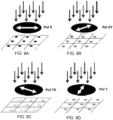
- a first feature of the array of features can be disposed over a first pixel of the array of imaging pixels, and a second feature of the array of features can be disposed over the first pixel and spatially displaced from the first feature.
- a first luminophore can be disposed within or over the first feature, and a second luminophore can be disposed within or over the second feature.
- the device further can include a radiation source configured to generate first photons having a first characteristic at a first time, and configured to generate second photons having a second characteristic at a second time.
- the second characteristic can be different than the first characteristic
- the second time can be different than the first time.
- the first pixel can selectively receive luminescence emitted by the first luminophore responsive to the first photons at the first time, and can selectively receive luminescence emitted by the second luminophore responsive to the second photons at the second time.
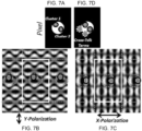
- the first photons having the first characteristic generate a first resonant pattern within the photonic structure at the first time, the first resonant pattern selectively exciting the first luminophore relative to the second luminophore.
- the second photons having the second characteristic generate a second resonant pattern within the photonic structure at the second time, the second resonant pattern selectively exciting the second luminophore relative to the first luminophore.
- the array of imaging pixels, the photonic structure, and the array of features optionally are monolithically integrated with one another.
- the photonic structure optionally includes a photonic crystal, a photonic superlattice, a microcavity array, or an array of plasmonic nanoantennas.
- the array of features optionally includes a plurality of wells.
- the first feature can include a first well within which the first luminophore is disposed, and the second feature can include a second well within which the second luminophore is disposed.
- the array of features optionally includes a plurality of posts.
- the first feature can include a first post upon which the first luminophore is disposed, and the second feature can include a second post upon which the second luminophore is disposed.
- the first and second characteristics optionally are selected independently from the group consisting of wavelength, polarization, and angle.
- the first characteristic optionally includes a first linear polarization
- the second characteristic optionally includes a second linear polarization that is different than the first linear polarization.
- the first linear polarization is substantially orthogonal to the second linear polarization, or optionally the first linear polarization is rotated relative to the second linear polarization by between about 15 degrees and about 75 degrees.
- the first characteristic optionally can include a first wavelength
- the second characteristic optionally can include a second wavelength that is different than the first wavelength.
- the radiation source optionally includes an optical component.
- the device further includes a controller coupled to the optical component and configured to control the optical component so as to impose the first characteristic on the first photons and configured to impose the second characteristic on the second photons.
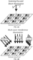
- the optical component includes a birefringent material configured to rotate the first photons to a first linear polarization responsive to a first control signal by the controller, and configured to rotate the second photons to a second linear polarization responsive to a second control signal by the controller.
- first and second photons optionally each irradiate the photonic structure at substantially the same angle as one another. Additionally, or alternatively, the first and second photons optionally each irradiate the photonic structure at an angle approximately normal to a major surface of the photonic structure. Additionally, or alternatively, the first and second photons optionally each irradiate the photonic structure at an angle approximately parallel to a major surface of the photonic structure.
- the second feature optionally is laterally displaced from the first feature.
- a third feature of the array of features optionally is disposed over the first pixel and spatially displaced from each of the first and second features.
- the device further optionally can include a third luminophore disposed within or over the third feature.
- the radiation source optionally can be configured to generate third photons having a third characteristic at a third time.
- the third characteristic can be different than the first and second characteristics, and the third time can be different than the first and second times.
- the first pixel selectively receives luminescence emitted by the third luminophore responsive to the third photons at the third time.
- a fourth feature of the array of features optionally is disposed over the first pixel and spatially displaced from each of the first, second, and third features.
- the device optionally further includes a fourth luminophore disposed within or over the fourth feature.
- the radiation source optionally is configured to generate fourth photons having a fourth characteristic at a fourth time.
- the fourth characteristic can be different than the first, second, and third characteristics, and the fourth time can be different than the first, second, and third times.
- the first pixel optionally selectively receives luminescence emitted by the fourth luminophore responsive to the fourth photons at the fourth time.
- the first luminophore is coupled to a first nucleic acid
- the second luminophore is coupled to a second nucleic acid
- the third luminophore is coupled to a third nucleic acid
- the fourth luminophore is coupled to a fourth nucleic acid.
- a third feature of the array of features optionally is disposed over a second pixel of the array of imaging pixels, and a fourth feature of the array of features optionally is disposed over the second pixel and spatially displaced from the third feature.
- the device optionally further includes a third luminophore disposed within or over the third feature, and a fourth luminophore disposed within or over the fourth feature.
- the second pixel selectively receives luminescence emitted by the third luminophore responsive to the first photons at the first time or responsive to the second photons at the second time.
- the second pixel selectively receives luminescence emitted by the fourth luminophore responsive to the first photons at the first time or responsive to the second photons at the second time.
- the first luminophore is coupled to a first nucleic acid
- the second luminophore is coupled to a second nucleic acid
- the third luminophore is coupled to a third nucleic acid
- the fourth luminophore is coupled to a fourth nucleic acid.
- the first and second features optionally each have a substantially circular cross-section.
- the photonic structure optionally includes a hexagonal lattice, and optionally the imaging pixels are rectangular.
- the radiation source optionally is configured to flood illuminate the photonic structure with the first and second photons. Additionally, or alternatively, the radiation source optionally includes a laser. Additionally, or alternatively, optionally the first and second photons independently have wavelengths between about 300 nm and about 800 nm.
- the first luminophore optionally is coupled to a first nucleic acid
- the second luminophore optionally is coupled to a second nucleic acid
- the device optionally includes at least one microfluidic feature in contact with the array of features and configured to provide a flow of one or more analytes to the first and second features.
- the first luminophore optionally is coupled to a first polynucleotide to be sequenced
- the second luminophore optionally is coupled to a second polynucleotide to be sequenced.
- the first polynucleotide is coupled to the first feature
- the second polynucleotide is coupled to the second feature.
- the device optionally further includes a first polymerase adding a first nucleic acid to a third polynucleotide that is complementary to and coupled to the first polynucleotide.
- the first nucleic acid optionally can be coupled to the first luminophore.
- the device optionally further includes a second polymerase adding a second nucleic acid to a fourth polynucleotide that is complementary to and coupled to the second polynucleotide.
- the second nucleic acid optionally can be coupled to the second luminophore.
- the device further can include a channel flowing a first liquid including the first and second nucleic acids and the first and second polymerases into or over the first and second features.
- a method for use in luminescent imaging.
- the method can include providing an array of imaging pixels, and providing a photonic structure disposed over the array of imaging pixels.
- the method further can include providing an array of features disposed over the photonic structure.
- a first feature of the array of features can be disposed over a first pixel of the array of imaging pixels, and a second feature of the array of features can be disposed over the first pixel and spatially displaced from the first feature.
- the method further can include providing a first luminophore disposed within or over the first feature, and providing a second luminophore disposed within or over the second feature.
- the method further can include generating by a radiation source first photons having a first characteristic at a first time, and generating by the radiation source second photons having a second characteristic at a second time.
- the second characteristic can be different than the first characteristic, and the second time can be different than the first time.
- the method further can include selectively receiving by the first pixel luminescence emitted by the first luminophore responsive to the first photons at the first time; and selectively receiving by the first pixel luminescence emitted by the second luminophore responsive to the second photons at the second time.
- the first photons having the first characteristic generate a first resonant pattern within the photonic structure at the first time, the first resonant pattern selectively exciting the first luminophore relative to the second luminophore.
- the second photons having the second characteristic generate a second resonant pattern within the photonic structure at the second time, the second resonant pattern selectively exciting the second luminophore relative to the first luminophore.
- the array of imaging pixels, the photonic structure, and the array of features optionally are monolithically integrated with one another.
- the photonic structure optionally includes a photonic crystal, a photonic superlattice, a microcavity array, or an array of plasmonic nanoantennas.
- the array of features optionally includes a plurality of wells.
- the first feature optionally can include a first well within which the first luminophore is disposed, and the second feature optionally can include a second well within which the second luminophore is disposed.
- the array of features can include a plurality of posts.
- the first feature optionally can include a first post upon which the first luminophore is disposed, and the second feature optionally can include a second post upon which the second luminophore is disposed.
- the first and second characteristics optionally can be selected independently from the group consisting of wavelength, polarization, and angle.
- the first characteristic optionally can include a first linear polarization
- the second characteristic optionally can include a second linear polarization that is different than the first linear polarization.
- the first linear polarization can be substantially orthogonal to the second linear polarization, or can be rotated relative to the second linear polarization by between about 15 degrees and about 75 degrees.
- the first characteristic optionally includes a first wavelength
- the second characteristic optionally includes a second wavelength that is different than the first wavelength.
- the radiation source optionally includes an optical component.
- the method optionally further includes controlling the optical component so as to impose the first characteristic on the first photons and so as to impose the second characteristic on the second photons.
- the optical component includes a birefringent material rotating the first photons to a first linear polarization responsive to a first control signal by a controller, and rotating the second photons to a second linear polarization responsive to a second control signal by the controller.
- first and second photons optionally each irradiate the photonic structure at substantially the same angle as one another. Additionally, or alternatively, the first and second photons optionally each irradiate the photonic structure at an angle approximately normal to a major surface of the photonic structure, or the first and second photons optionally each irradiate the photonic structure at an angle approximately parallel to a major surface of the photonic structure.
- the second feature optionally is laterally displaced from the first feature.
- a third feature of the array of features optionally is disposed over the first pixel and spatially displaced from each of the first and second features.
- the method further includes providing a third luminophore disposed within or over the third feature, and generating third photons having a third characteristic at a third time.
- the third characteristic optionally can be different than the first and second characteristics, and the third time optionally can be different than the first and second times.
- the method optionally further can include selectively receiving by the first pixel luminescence emitted by the third luminophore responsive to the third photons at the third time.
- a fourth feature of the array of features is disposed over the first pixel and spatially displaced from each of the first, second, and third features.
- the method optionally further includes providing a fourth luminophore disposed within or over the fourth feature, and generating fourth photons having a fourth characteristic at a fourth time.
- the fourth characteristic optionally can be different than the first, second, and third characteristics
- the fourth time optionally can be different than the first, second, and third times.
- the method optionally further can include selectively receiving by the first pixel luminescence emitted by the fourth luminophore responsive to the fourth photons at the fourth time.
- the first luminophore is coupled to a first nucleic acid
- the second luminophore is coupled to a second nucleic acid
- the third luminophore is coupled to a third nucleic acid
- the fourth luminophore is coupled to a fourth nucleic acid.
- a third feature of the array of features optionally can be disposed over a second pixel of the array of imaging pixels, and a fourth feature of the array of features is disposed over the second pixel and spatially displaced from the third feature.
- the method optionally further includes providing a third luminophore disposed within or over the third feature, and providing a fourth luminophore disposed within or over the fourth feature.
- the method optionally further includes selectively receiving by the second pixel luminescence emitted by the third luminophore responsive to the first photons at the first time or responsive to the second photons at the second time; and selectively receiving by the second pixel luminescence emitted by the fourth luminophore responsive to the first photons at the first time or responsive to the second photons at the second time.
- the first luminophore is coupled to a first nucleic acid
- the second luminophore is coupled to a second nucleic acid
- the third luminophore is coupled to a third nucleic acid
- the fourth luminophore is coupled to a fourth nucleic acid.
- the first and second features optionally each have a substantially circular cross-section.
- the photonic structure optionally includes a hexagonal lattice, and the imaging pixels optionally are rectangular.
- the method optionally includes flood illuminating the photonic structure with the first and second photons. Additionally, or alternatively, the method optionally includes generating the first and second photons with a laser. Additionally, or alternatively, optionally the first and second photons independently have wavelengths between about 300 nm and about 800 nm.
- the first luminophore optionally is coupled to a first nucleic acid
- the second luminophore optionally is coupled to a second nucleic acid
- the method optionally further includes providing at least one microfluidic feature in contact with the array of features and flowing, by the at least one microfluidic feature, one or more analytes to the first and second features.
- the first luminophore optionally is coupled to a first polynucleotide to be sequenced
- the second luminophore optionally is coupled to a second polynucleotide to be sequenced.
- the first polynucleotide is coupled to the first feature
- the second polynucleotide optionally is coupled to the second feature.
- the method optionally includes adding, by a first polymerase, a first nucleic acid to a third polynucleotide that is complementary to and coupled to the first polynucleotide.
- the first nucleic acid optionally can be coupled to the first luminophore.
- the method optionally further includes adding, by a second polymerase, a second nucleic acid to a fourth polynucleotide that is complementary to and coupled to the second polynucleotide.
- the second nucleic acid optionally can be coupled to the second luminophore.
- the method further includes flowing, by a channel, a first liquid including the first and second nucleic acids and the first and second polymerases into or over the first and second features.
- a device for use in luminescent imaging.
- the device can include an array of imaging pixels, and a photonic structure disposed over the array of imaging pixels.
- the device further can include an array of features disposed over the photonic structure.
- a first feature of the array of features can be disposed over a first pixel of the array of imaging pixels, and a second feature of the array of features can be disposed over the first pixel and spatially displaced from the first feature.
- the photonic structure can be tuned to selectively irradiate the first feature with light of a first polarization compared to light of a second polarization.
- the photonic structure can be tuned to selectively irradiate the second feature with light of a second polarization compared to light of the first polarization.
- the device further includes a radiation source configured to generate first photons having the first polarization at a first time, and configured to generate second photons having the second polarization at a second time.
- a radiation source configured to generate first photons having the first polarization at a first time, and configured to generate second photons having the second polarization at a second time.
- the device optionally further includes a first luminophore disposed within or over the first feature and a second luminophore disposed within or over the second feature.
- the device optionally further includes a first target analyte disposed within or over the first feature and a second target analyte disposed within or over the second feature.
- the first target analyte optionally can be different from the second target analyte.
- the first and second target analytes optionally include nucleic acids having different sequences.
- Embodiments of the present invention provide photonic structure-based devices and compositions for use in luminescent imaging of multiple sites within a pixel, and methods of using the same.
- the term "photonic structure” means a periodic structure, including one or more optically transparent materials, that selectively affects the propagation of radiation having a particular characteristic, e.g., at a wavelength, an angle, and at a polarization.
- the photonic structure can selectively propagate radiation having such characteristic, e.g., at the wavelength, the angle, and the polarization, through the structure or at the same angle or a different angle out of the structure, and the field strength of such radiation can have a selected pattern within the photonic structure.
- the structure can selectively inhibit propagation of radiation having a different characteristic, e.g., at a different wavelength, angle, and/or polarization, through the structure or at a different angle out of the structure, and/or the field strength of such radiation can have a different selected pattern within the photonic structure.
- the material(s) of the photonic structure can include features that are distributed in one or more dimensions, e.g., in one dimension, in two dimensions, or in three dimensions.
- the shape, size, and distribution of the features of the photonic structure, as well as the refractive index of the material(s), can be tuned so as select the particular radiation characteristic(s), e.g., wavelength(s), angle(s), or polarization(s), that can propagate through or at an angle out of the photonic structure, and/or so as to select the pattern of the field strength of such radiation within the photonic structure.
- exemplary photonic structures include, but are not limited to, photonic crystals, photonic superlattices, microcavity arrays, and arrays of plasmonic nanoantennas.
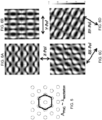
- a photonic crystal means a photonic structure including one or more materials that include a periodic variation of refractive index on the order of the wavelength of light.
- a photonic crystal can include a material that extends in three dimensions, e.g., has a length, a width, and a thickness. The material can have two major surfaces that each lie within a plane defined by the length and the width, and separated from one another by the thickness.
- the material can be patterned in two or more dimensions so as to define a photonic band structure within which radiation having particular characteristic(s), e.g., wavelength(s), angle(s), or polarization(s), can propagate through or at an angle out of the photonic crystal, and/or so as to select the pattern of the field strength of such radiation within the photonic crystal.
- the pattern can include, for example, a plurality of features such as wells or posts that are defined within the material, e.g., through one or both of the major surfaces of the material, the material being absent within or between the features, such as within the wells or between the posts.
- a space within or between the features can be filled with one or more additional materials that respectively can have different refractive indices than that of the material and than that of one another.
- the particular characteristic(s) of radiation, e.g., wavelength(s), angle(s), or polarization(s), that propagate or do not propagate through, or at an angle out of, the photonic crystal can be based on the refractive indices of the material and of any additional materials disposed within the features or between the features, as well as based on the characteristics of the features, such as the shape, size, and distribution of the features.
- the features can be all the same shape, size, and/or distribution as one another.
- the terms "photonic superlattice” and “PhC superlattice” mean a photonic structure that selectively affects the propagation of radiation having first and second characteristics, e.g., at first and second wavelength(s), angle(s), or polarization(s), compared to radiation having third characteristics, e.g., at a third wavelength, angle, or polarization.
- the field strength of the radiation having the first characteristics can have a first pattern
- the field strength of the radiation having the second characteristics can have a second pattern that is different from the first pattern.
- the third wavelength can occur between the first and second wavelengths in the electromagnetic spectrum.
- the photonic superlattice can selectively propagate radiation having the first and second characteristics, e.g., at the first and second wavelength(s), angle(s), or polarization(s), through the photonic superlattice or at an angle out of the photonic superlattice, and the patterns of the field strengths for the radiation having the first and second characteristics optionally can be different than one another.
- the photonic superlattice can selectively inhibit propagation of radiation having the first and second characteristics, e.g., at the first and second wavelength(s), angle(s), or polarization(s), through the photonic superlattice or at an angle out of the photonic superlattice.
- the photonic superlattice can selectively propagate radiation having third characteristics, e.g., at the third wavelength, angle, or polarization, through the photonic superlattice or at an angle out of the photonic superlattice.
- the photonic superlattice can selectively inhibit propagation of radiation having third characteristics, e.g., at the third wavelength, angle, or polarization, through the structure or at an angle out of the structure.
- the material(s) can include features that are distributed in one or more dimensions, e.g., in one dimension, in two dimensions, or in three dimensions.
- the shape, size, and distribution of the features, as well as the refractive index of the material(s), can be tuned so as select the particular characteristics of radiation, e.g., wavelength(s), angle(s), or polarization(s), that can propagate through or at an angle out of the photonic superlattice, as well as the patterns of field strength of such characteristics, and so as to select the particular characteristics of radiation that do not propagate substantially through or at an angle out of the photonic superlattice.
- a photonic superlattice can include a material that extends in three dimensions, e.g., has a length, a width, and a thickness.
- the material can have two major surfaces that each lie within a plane defined by the length and the width, and separated from one another by the thickness.
- the material can be patterned in two or more dimensions so as to define a photonic band structure that permits propagation of radiation having at least first and second characteristics, e.g., wavelength(s), angle(s), or polarization(s), within, or at an angle out of, the plane defined by the length and the width, and that inhibits propagation of at least radiation having third characteristics, e.g., a third wavelength, angle, or polarization, within, or at an angle out of, the material.
- the pattern can include, for example, a plurality of features such as wells or posts that are defined within the material, e.g., through one or both of the major surfaces of the material, the material being absent within or between the features, such as within the wells or between the posts.
- a space within or between the features can be filled with one or more additional materials that respectively can have different refractive indices than that of the material and than that of one another.
- the particular characteristics of radiation that propagate or do not propagate through, or at an angle out of, the photonic superlattice can be based on the refractive indices of the material and of any additional materials disposed within the features or between the features, as well as based on the characteristics of the features, such as the shape, size, and distribution of the features.
- Some of the features optionally can differ in at least one characteristic, e.g., shape, size, or distribution, from others of the features.
- microcavity array means a periodic two-dimensional arrangement of photonic microresonators that support multiple (e.g., at least two, at least three, or at least four) resonances that can be excited independently of one another by changing a characteristic of an excitation source, such as the wavelength, polarization, or angle of the excitation source.
- exemplary microcavity arrays that can be used in the present devices, compositions, and methods, see Altug et al., "Polarization control and sensing with twodimensional coupled photonic crystal microcavity arrays," Opt. Lett. 30: 1422-1428 (2011 ), the entire contents of which are incorporated by reference herein.
- array of plasmonic nanoantennas means a periodic twodimensional arrangement of plasmonic nanostructures that support multiple (e.g., at least two, at least three, or at least four) resonances that can be excited independently of one another by changing a characteristic of an excitation source, such as the wavelength, polarization, or angle of the polarization source.
- exemplary plasmonic nanoantennas that can be used in the present devices, compositions, and methods, see Regmi et al., “Nanoscale volume confinement and fluorescence enhancement with double nanohole aperture,” Scientific Reports 5: 15852-1-5 (2015 ), the entire contents of which are incorporated by reference herein.
- One or more of the materials of the photonic structure can be or include a "dielectric material,” meaning a fluidic, solid, or semi-solid material that is optically transparent and is an electrical insulator.
- fluidic dielectric materials include gases such as air, nitrogen, and argon, as well as liquids such as such as water, aqueous solvents, and organic solvents.
- solid dielectric materials include glasses (e.g., inorganic glasses such as silica, or modified or functionalized glasses) and polymers (such as acrylics, polystyrene, copolymers of styrene and other materials, polypropylene, polyethylene, polybutene, polyurethanes, TEFLON TM , cyclic olefins, polyimides, or nylon).
- glasses e.g., inorganic glasses such as silica, or modified or functionalized glasses
- polymers such as acrylics, polystyrene, copolymers of styrene and other materials, polypropylene, polyethylene, polybutene, polyurethanes, TEFLON TM , cyclic olefins, polyimides, or nylon.
- semi-solid dielectric materials include gels, such as hydrogels.
- one or more materials of the photonic structure can be or include a solid semiconductor material that is optically transparent.
- gel is intended to mean a semi-solid or semi-rigid material that is permeable to liquids and gases.
- gel material can swell when liquid is taken up and can contract when liquid is removed by drying.
- Exemplary gels can include, but are not limited to, those having a colloidal structure, such as agarose or a hydrogel; polymer mesh structure, such as gelatin; or cross-linked polymer structure, such as polyacrylamide, SFA (see, for example, US 2011/0059865 , the entire contents of which are incorporated by reference herein) or PAZAM (see, for example, US 2014/0079923 , the entire contents of which are incorporated by reference herein).
- Particularly useful gel material will conform to the shape of a well or other concave feature where it resides.
- the term "well” means a discrete concave feature in a material having a surface opening (aperture) that is completely surrounded by interstitial region(s) of the surface.
- a well can have characteristics such as size (e.g., volume, diameter, and depth), cross-sectional shape (e.g., round, elliptical, triangular, square, polygonal, star shaped (having any suitable number of vertices), irregular, or having concentric wells separated by a dielectric material), and distribution (e.g., spatial locations of the wells within the dielectric material, e.g., regularly spaced or periodic locations, or irregularly spaced or aperiodic locations).
- the cross section of a well can be, but need not necessarily be, uniform along the length of the well.
- post means a discrete convex feature protruding from the surface of a material and that is completely surrounded by interstitial region(s) of the surface.
- a post can have characteristics such as size (e.g., volume, diameter, and depth), shape (e.g., round, elliptical, triangular, square, polygonal, star shaped (having any suitable number of vertices), irregular, or having concentric posts separated by a dielectric material), and distribution (e.g., spatial locations of the posts protruding from the surface of the dielectric material, e.g., regularly spaced or periodic locations, or irregularly spaced or aperiodic locations).
- the cross section of a post can be, but need not necessarily be, uniform along the length of the post.
- surface means a part or layer of a material that is in contact with another material.
- an interstitial region is intended to mean an area in a material or on a surface that separates areas of the material or surface.
- an interstitial region can separate one feature of a photonic structure from another feature of a photonic structure, or an interstitial region can separate one site of an array from another site of the array.
- the term “luminescent” means emitting cold body radiation
- the term “luminophore” means an item that is luminescent.
- the term “luminescent” is intended to be distinct from incandescence which is radiation emitted from a material as a result of heat. Generally luminescence results when an energy source displaces an electron of an atom out of its lowest energy ground state into a higher energy excited state; then the electron returns the energy in the form of radiation so it can fall back to its ground state.
- a particularly useful type of luminescent item is one that emits cold body radiation when energy is provided by excitation radiation.
- photoluminescent items include “fluorescent” items that emit cold body radiation relatively quickly (e.g., less than a millisecond) after excitation radiation, and “phosphorescent” items that emit cold body radiation relatively slowly (e.g., greater than or equal to a millisecond) after excitation radiation.
- Photoluminescence can be perceived as emission of radiation by an item at a wavelength that is a result of irradiating the item at another wavelength.
- Another useful type of luminescent item is one that emits cold body radiation when energy is provided by a chemical or biological reaction. Such items can be referred to as "chemiluminescent.”
- any of a variety of signals can be detected in a method set forth herein including, for example, an optical signal such as absorbance of radiation, luminescence emission, luminescence lifetime, luminescence polarization, or the like; Rayleigh and/or Mie scattering; or the like.
- Exemplary labels that can be detected in a method set forth herein include, without limitation, a fluorophore, luminophore, chromophore, nanoparticle (e.g., gold, silver, carbon nanotubes), or the like.
- feature means a distinctive variation in the structure or composition of a material such as a solid support.
- the variation is also repeated in the structure or composition of the material.
- a collection of the features can form an array or lattice in or on the material.
- Exemplary features include, but are not limited to wells, posts, ridges, channels, sites bearing analytes, layers of a multilayer material, areas in or on a material having a chemical composition that differ from the chemical composition of other areas in or on the material and the like.
- a feature can have characteristics such as size (e.g., volume, diameter, and depth), shape (e.g., round, elliptical, triangular, square, polygonal, star shaped (having any suitable number of vertices), irregular, or having concentric features separated by a dielectric material), and distribution (e.g., spatial locations of the features within the dielectric material, e.g., regularly spaced or periodic locations, or irregularly spaced or aperiodic locations).
- the cross section of a feature can be, but need not necessarily be, uniform along the length of the feature.
- site means a location in an array for a particular species of molecule or cell (or other analyte).
- a site can contain only a single molecule (or cell or other analyte) or it can contain a population of several molecules (or cells or analytes) of the same species.
- sites are present on a material prior to attaching a particular analyte.
- the site is created by attachment of a molecule or cell (or other analyte) to the material.
- Sites of an array are typically discrete. The discrete sites can be contiguous or they can have spaces between each other. It will be understood that a site is a type of feature.
- a feature can function as a component of a lattice, array or both.
- array means a population of sites that can be differentiated from each other according to relative location.
- the term "pitch,” when used in reference to features of a lattice (e.g. photonic structure) or array, is intended to refer to the center-to-center spacing for adjacent features of the lattice or array.
- a pattern of features can be characterized in terms of average pitch. The pattern can be ordered such that the coefficient of variation around the average pitch is small, or the pattern can be random in which case the coefficient of variation can be relatively large. In either case, the average pitch can be, for example, at least about on the order of a wavelength of light in one or more regions of the spectrum.
- the pitch can correspond to wavelengths in one or more of the visible spectrum (about 380-700 nm), UV spectrum (less than about 380 nm to about 10 nm) and IR spectrum (greater than about 700 nm to about 1 mm).
- features can have different pitches than one another in different directions.
- different types of features can have different pitches and patterns than one another.
- the pitch for the features of one type e.g. in a first lattice
- can differ from the pitch for features of another type e.g. in a second lattice).
- the term "random" can be used to refer to the spatial distribution, e.g., arrangement, of locations on a surface.
- one or more features (e.g., wells or posts) of a photonic structure or a photonic superlattice can be randomly spaced such that nearest neighbor features, which can be of the same type or different type than one another, have variable spacing between each other.
- the spacing between features of the same type or a different type than one another can be ordered, for example, forming a regular pattern such as a rectilinear grid or a hexagonal grid.
- nucleotide or “nucleic acid” is intended to mean a molecule that includes a sugar and at least one phosphate group, and optionally also includes a nucleobase.
- a nucleotide that lacks a nucleobase can be referred to as "abasic.”
- Nucleotides include deoxyribonucleotides, modified deoxyribonucleotides, ribonucleotides, modified ribonucleotides, peptide nucleotides, modified peptide nucleotides, modified phosphate sugar backbone nucleotides, and mixtures thereof.
- nucleotides examples include adenosine monophosphate (AMP), adenosine diphosphate (ADP), adenosine triphosphate (ATP), thymidine monophosphate (TMP), thymidine diphosphate (TDP), thymidine triphosphate (TTP), cytidine monophosphate (CMP), cytidine diphosphate (CDP), cytidine triphosphate (CTP), guanosine monophosphate (GMP), guanosine diphosphate (GDP), guanosine triphosphate (GTP), uridine monophosphate (UMP), uridine diphosphate (UDP), uridine triphosphate (UTP), deoxyadenosine monophosphate (dAMP), deoxyadenosine diphosphate (dADP), deoxyadenosine triphosphate (dATP), deoxythymidine monophosphate (dTMP), deoxythymidine diphosphate (dTDP), deoxy
- nucleotide or “nucleic acid” also is intended to encompass any nucleotide analogue which is a type of nucleotide that includes a modified nucleobase, sugar and/or phosphate moiety.
- modified nucleobases that can be included in a polynucleotide, whether having a native backbone or analogue structure, include, inosine, xathanine, hypoxathanine, isocytosine, isoguanine, 2-aminopurine, 5-methylcytosine, 5-hydroxymethyl cytosine, 2-aminoadenine, 6-methyl adenine, 6-methyl guanine, 2-propyl guanine, 2-propyl adenine, 2-thiouracil, 2-thiothymine, 2-thiocytosine, 15 -halouracil, 15 -halocytosine, 5-propynyl uracil, 5-propynyl cytosine, 6-azo urac
- polynucleotide refers to a molecule that includes a sequence of nucleotides that are bonded to one another.
- examples of polynucleotides include deoxyribonucleic acid (DNA), ribonucleic acid (RNA), and analogues thereof.
- a polynucleotide can be a single stranded sequence of nucleotides, such as RNA or single stranded DNA, a double stranded sequence of nucleotides, such as double stranded DNA, or can include a mixture of a single stranded and double stranded sequences of nucleotides.
- Double stranded DNA includes genomic DNA, and PCR and amplification products. Single stranded DNA (ssDNA) can be converted to dsDNA and vice-versa. The precise sequence of nucleotides in a polynucleotide can be known or unknown.
- polynucleotides a gene or gene fragment (for example, a probe, primer, expressed sequence tag (EST) or serial analysis of gene expression (SAGE) tag), genomic DNA, genomic DNA fragment, exon, intron, messenger RNA (mRNA), transfer RNA, ribosomal RNA, ribozyme, cDNA, recombinant polynucleotide, synthetic polynucleotide, branched polynucleotide, plasmid, vector, isolated DNA of any sequence, isolated RNA of any sequence, nucleic acid probe, primer or amplified copy of any of the foregoing.
- a gene or gene fragment for example, a probe, primer, expressed sequence tag (EST) or serial analysis of gene expression (SAGE) tag
- genomic DNA genomic DNA fragment, genomic DNA fragment, exon, intron, messenger RNA (mRNA), transfer RNA, ribosomal RNA, ribozyme, cDNA, recombinant polynucleotide, synthetic polynu
- “chemically coupled” is intended to mean an attachment between a first member and a second member.
- such an attachment is normally irreversible under the conditions in which the attached members are used.
- such an attachment is reversible but persists for at least the period of time in which it is used for one or more steps of an analytical or preparative technique set forth herein (e.g. an analytical step of detecting a subunit of a polymer).
- Such attachment can be formed via a chemical bond, e.g., via a covalent bond, hydrogen bond, ionic bond, dipole-dipole bond, London dispersion forces, or any suitable combination thereof.
- Covalent bonds are only one example of an attachment that suitably can be used to couple a first member to a second member.
- Other examples include duplexes between oligonucleotides, peptide-peptide interactions, and hapten-antibody interactions such as streptavidin-biotin, streptavidin-desthiobiotin, and digoxigenin-antidigoxigenin.
- an attachment can be formed by hybridizing a first polynucleotide to a second polynucleotide that inhibits detachment of the first polynucleotide from the second polynucleotide.
- an attachment can be formed using physical or biological interactions, e.g., an interaction between a first protein and a second protein that inhibits detachment of the first protein from the second protein.
- a "polymerase” is intended to mean an enzyme having an active site that assembles polynucleotides by polymerizing nucleotides into polynucleotides.
- a polymerase can bind a primed single stranded polynucleotide template, and can sequentially add nucleotides to the growing primer to form a polynucleotide having a sequence that is complementary to that of the template.
- compositions and devices that include photonic structures, such as for single color or multicolor luminescence signal enhancement from analytes (e.g. DNA clusters) in one or more excitation and/or luminescence emission bands, optionally at normal incidence of excitation.
- analytes e.g. DNA clusters
- monolithic integration of photonic and microfluidic chips on top of CMOS imaging arrays can be used to reduce the size of, e.g., miniaturize, DNA sequencers.
- Throughput of CMOS-based sequencing devices can be limited by the size of imaging pixels. For example, relatively large pixel sizes can be useful for providing sufficient signal collection from individual DNA molecules or clusters of identical molecules.
- pixels can be made smaller so as to increase throughput, such size reduction can reduce full well capacity and can increase cross-talk between pixels, thereby reducing the signal-to-noise ratio (SNR) of the imaging, and the sequencing.
- SNR signal-to-noise ratio
- Such an approach also can increase the cost of fabricating the imaging array, e.g., by increasing the amount of engineering of the imaging array as well as the integration of such imaging array with photonic and/or microfluidic components.
- an alternative way of increasing throughout by providing more testing sites per device can involve introducing multiple luminescence sites (e.g., DNA clusters, microarray reaction chambers, or the like) per pixel.
- the present compositions, devices, and methods can image multiple sites, each of which can include a respective analyte, using an imaging pixel by selectively exciting different sites at different times than one another using an excitation source, and obtaining a respective image at each such time.
- an array of imaging pixels can be provided, and multiple sites can be disposed over each such imaging pixel.
- the present multi-site per pixel configuration can significantly increase the number of sites that can be imaged using a given pixel array.
- the pixel would receive luminescence from each such site simultaneously with one another, thus impeding the ability to distinguish between luminescence from one such site and luminescence from another such site based on an electrical signal that the pixel generates responsive to receiving such luminescence.
- Optical techniques such as provided herein can be used so as selectively to excite only a single one of the multiple sites disposed over a given imaging pixel at a given time, so as to obtain an electrical signal from that pixel responsive to luminescence just from that site at that time, and subsequently to excite a second one of the multiple sites over that imaging pixel at a second time, so as to obtain a second electrical signal from that pixel responsive to luminescence from that second site.
- the luminescence from the two sites can be distinguished from one another based on the electrical signals obtained from the imaging pixel at the two times.
- compositions, devices, and methods can provide luminescent imaging of a greater number of sites than the number of pixels in an imaging array, e.g., an integer multiple n of the number of pixels, where n is greater than or equal to 2, or 3, or 4, or 5, or greater than 5.
- the different sites disposed over an imaging pixel can be selectively excited by selectively directing excitation photons to respective ones of the sites at different times than one another.
- a focused laser beam can be scanned over the different sites at different times than one another so as to selectively excite ones of the different sites at such times, the pixel generating electrical signals at such time responsive to the luminescence from the particular site being excited.
- the sites can be irradiated at a first time with any suitable number of laser beams that interfere with one another in such a manner as to generate a first optical intensity pattern that selectively excites one of the sites at the first time, and can be irradiated at a second time with any suitable number of laser beams that interfere with one another in such a manner as to generate a second optical intensity pattern that selectively excites another one of the sites at the second time.
- the pixel can generate respective electrical signals at the first and second times responsive to luminescence from the respective sites.
- the sites can be disposed over or within a photonic structure that is disposed over the imaging pixel.
- the photonic structure can be configured so as selectively to excite one of the sites over the pixel responsive to irradiation with photons having a first characteristic at a first time, and selectively to excite another one of the sites over the pixel responsive to irradiation with photons having a second characteristic at a second time.
- the pixel can generate respective electrical signals at the first and second times responsive to luminescence from the respective sites.
- the present photonic structure-based devices, compositions, and methods are compatible with previously known epifluorescence microscopy and microscope scanning systems (such as those in commercially available sequencing platforms such as produced by Illumina, Inc. (San Diego, California)) that, in some circumstances, can use multiple fluorescent dyes excited at normal and imaged at normal incidence in various spectral windows. Such dyes can be coupled to nucleotides so as to facilitate sequencing polynucleotides such as DNA.
- the present photonic structure-based devices, compositions, and methods suitably can be used in any type of luminescent imaging or any other suitable application, and are not limited to use in sequencing polynucleotides such as DNA.
- Patterning of dielectric substrates previously has been employed successfully to control the size and uniformity of polynucleotide clusters, and to increase the density of such clusters so as to improve throughput of sequencing. See for example, US Pat. App. Publ. No. 2014/0243224 A1 , which is incorporated herein by reference.
- reduction in cluster size has resulted in a considerable reduction in the amount of collected multicolor fluorescence signal.
- detection of weak multicolor fluorescence signals from large sampling areas can become increasingly difficult as the number of labeled nucleotides in DNA clusters is reduced (e.g., down to single-molecule levels or the resolution limits of the imaging system).
- Significant fluorescence signal enhancement therefore can be helpful to facilitate nucleotide identification and increase the throughput of next generation SBS systems.
- periodic patterning of materials in the proximity of fluorescently marked biomolecules can enhance fluorescence signal by creating one- or two-dimensional waveguides with a periodic variation of the refractive index in on the order of wavelength of light.
- waveguides which can be referred to as photonic crystals (PhCs), photonic lattices, photonic crystal lattices, or PhC lattices, can support high-Q resonant modes that can boost fluorescent signals by resonantly enhancing fluorophore excitation, fluorescence collection, or both.
- PhC lattices also can be used in multicolor fluorescence signal enhancement.
- dual-excitation fluorescence signal boost has been achieved with PhCs by resonant enhancement of excitation at different wavelengths that requires adjustment of the angle of incidence of excitation source to match the resonances supported by the PhC.
- U.S. Patent No. 8,344,333 to Lu et al. the entire contents of which are incorporated by reference herein.
- FIG. 1A schematically illustrates a perspective view of an exemplary photonic structure-based device for use in luminescent imaging of a site within a pixel.
- the device illustrated in FIG. 1A includes an imaging pixel, such as a complementary metal oxide semiconductor (CMOS) based image sensor; a photonic structure such as a PhC layer disposed over the imaging pixel; and a nanowell defined within a third material disposed over the PhC layer.
- CMOS complementary metal oxide semiconductor
- the PhC layer can include a first material (shown in black) having a refractive index of n 1 , and regular patterns of uniformly shaped and sized wells that are defined within the first material and are filled with a second material (shown in white) having a refractive index of n 2 , where n 1 and n 2 are different than each other.
- a site including one or more luminophores, e.g., one or more analytes respectively coupled to luminophores, e.g., one or more nucleotides respectively coupled to luminophores, can be disposed within the nanowell.
- the luminophore(s) can be disposed in the near field of the PhC layer and excited evanescently by the excitation wavelengths, e.g., photons having suitable characteristics (illustrated as large downward-pointing arrow in FIG. 1A ).
- the imaging pixel can be suitably electronically coupled to a detection circuit (not specifically illustrated), which can be configured so as to receive and analyze an electrical signal generated by the imaging pixel responsive to luminescence generated by the luminophore(s).
- a detection circuit not specifically illustrated
- the imaging pixel is illustrated in FIG. 1A as having a dimension of 1.75 ⁇ m on each side, it should be appreciated that imaging pixels of any suitable dimensions can be used.
- FIG. 1B schematically illustrates a perspective view of an exemplary array of sites within an array of devices such as illustrated in FIG. 1A , wherein each site (represented as a black circle) corresponds to a pixel (represented as a rectangle). That is, the exemplary array illustrated in FIG. 1B includes one site for each pixel.
- each such device can include any suitable number and type of materials.
- FIG. 1C schematically illustrates a cross-sectional view of an exemplary device such as illustrated in FIG. 1A .
- a PhC layer can be disposed over any suitable imaging pixel such as known in the art.
- the PhC layer can include a first material, such as silicon nitride (SiN), that is patterned so as to define a photonic crystal.
- a second material such as tantalum oxide (TaO)
- TaO tantalum oxide
- the nanowell can be defined in a third material, such as SiN, and a fourth material such as TaO can be disposed over the nanowell.
- a single nanowell can be disposed over each imaging pixel. As such, each imaging pixel can receive luminescence from luminophore(s) disposed within the nanowell over that pixel, and generate a suitable electronic signal responsive to receipt of such luminescence.
- FIG. 2A schematically illustrates a perspective view of exemplary excitation of the array of sites illustrated in FIG. 1B .
- the array of sites can be irradiated with uniform (flat-top) illumination from a single optical source, such as a laser. Such irradiation suitably can excite one or more resonant modes within the PhC beneath such sites (such as shown in FIGS. 1A and 1C ).
- FIG. 2B schematically illustrates simulated exemplary field strengths within an array of devices such as illustrated in FIGS. 1A and 1C responsive to excitation such as illustrated in FIG. 2A .
- the features of the PhC can be tuned so as provide a relatively high field strength in a location disposed immediately beneath nanowell 200, thus selectively exciting luminophore(s) at the site disposed within that nanowell.
- the number of sites can be increased as an integer multiple n > 1 of the number of imaging pixels by selectively exciting different ones of such sites at different times than one another.
- FIG. 3A schematically illustrates a perspective view of an exemplary array of sites such as provided herein, wherein multiple sites correspond to a pixel.
- four sites (respectively illustrated as circles having different fills than one another) are provided per pixel (represented as rectangles), although it should be appreciated that any suitable number of sites can be provided per pixel, e.g., 2 or more sites per pixel, 3 or more sites per pixel, 4 or more sites per pixel, or 5 or more sites per pixel.
- Such sites can be provided using any suitable features.
- FIG. 3B schematically illustrates a cross-sectional view of a device such as provided herein, wherein multiple sites correspond to a pixel such as illustrated in FIG. 3A .
- an optional photonic structure can be disposed over any suitable imaging pixel such as known in the art.
- the optional photonic crystal can include a first material, such as silicon nitride (SiN), that is disposed over the imaging pixel; a second material, such as silicon dioxide (SiOz) that is disposed over the first material; and a photonic crystal including a pattern of a third material, such as SiN, and a fourth material, such as SiO 2 .
- a fifth material such as tantalum oxide (TaO)
- TaO tantalum oxide
- a plurality of features such as a plurality of nanowells, can be defined in a sixth material, such as SiOz, and a seventh material such as TaO can be disposed over the plurality of nanowells.
- multiple features e.g., multiple nanowells, can be disposed over each imaging pixel.
- each imaging pixel can receive luminescence at different times from luminophore(s) disposed within or over each such feature, e.g., within each such nanowell, over that pixel, and generate a suitable electronic signal responsive to receipt of such luminescence at such different times.
- the imaging pixel, the optional photonic structure, and the features optionally can be monolithically integrated with one another.
- the optional photonic structure illustrated in FIG. 3B is intended to be exemplary, and not limiting.
- the photonic structure can include a photonic crystal, or a photonic superlattice, or a microcavity array, or an array of plasmonic nanoantennas.
- Sites such as provided herein, e.g., with reference to FIGS. 3A-3B selectively can be excited using any suitable technique.
- a photonic structure optionally can be omitted, and the sites over a given pixel can be selectively excited by directing photons to such sites.
- a focused laser beam can be scanned over the different sites at different times than one another so as to selectively excite ones of the different sites at such times, the pixel generating electrical signals at such time responsive to the luminescence from the particular site being excited.
- FIG. 4A schematically illustrates a perspective view of exemplary excitation of selected sites of the array of sites illustrated in FIG. 3A using scanning focused beam illumination such as provided herein.
- precise control of excitation beams can be achieved using high-precision free-space beam steering, or by sample manipulation, in a manner similar to that described in Hahn et al., "Laser scanning lithography for surface micropatterning on hydrogels," Adv. Mater. 17: 2939-2942 (2005 ) or that described in Brakenhoff et al., "Confocal light scanning microscopy with high-aperture immersion lenses,” J. Microsc. 117: 219-232 (1997 ), the entire contents of both of which are incorporated by reference herein.
- the sites can be irradiated at a first time with any suitable number of laser beams that interfere with one another in such a manner as to generate a first optical intensity pattern that selectively excites one of the sites at the first time, and can be irradiated at a second time with any suitable number of laser beams that interfere with one another in such a manner as to generate a second optical intensity pattern that selectively excites another one of the sites at the second time.
- the pixel can generate respective electrical signals at the first and second times responsive to luminescence from the respective sites.
- FIG. 4B schematically illustrates a perspective view of exemplary excitation of selected sites of the array of sites illustrated in FIG. 3A using multi-laser interference illumination such as provided herein.
- the sites selectively can be irradiated using multi-laser interference illumination similar to that described in van Wolferen et al., "Laser interference lithography,” in Lithography: Principles, Processes and Materials, pages 133-148, Theodore Hennessy, Ed., Nova Science Publishers, Inc. (2011 ), or in He et al., "Polarization control in flexible interference lithography for nano-patterning of different photonic structures with optimized contrast," Optics Express 11518-11525 (May 4, 2015 ), the entire contents of each of which are incorporated by reference herein.
- the sites can be disposed over or within a photonic structure that is disposed over the imaging pixel.
- the photonic structure can be configured so as selectively to excite one of the sites over the pixel responsive to irradiation with photons having a first characteristic at a first time, and selectively to excite another one of the sites over the pixel responsive to irradiation with photons having a second characteristic at a second time.
- the pixel can generate respective electrical signals at the first and second times responsive to luminescence from the respective sites.
- FIG. 5 schematically illustrates an exemplary photonic structure such as can be included in a device such as provided herein and illustrated in FIGS. 3A3B . In the particular embodiment illustrated in FIG.
- the photonic structure can include a photonic crystal (PhC), but it should be appreciated that the photonic structure can include a photonic superlattice, or a microcavity array, or an array of plasmonic nanoantennas.
- the exemplary PhC illustrated in FIG. 5 includes a hexagonal array of features defined within a material, where the spacing ⁇ PhC between the features is on the order of the wavelength of excitation light ⁇ excitation .
- the photonic structure e.g., PhC
- the photonic structure can be tuned (e.g., the features of the PhC can be selected) such that photons having different characteristics than one another can selectively excite different resonances within the PhC.
- Photonic structure design parameters can be computationally adjusted so as to tune resonances to respective desired locations and/or excitation or emission peaks of luminophores, for example using one or more of Finite-Difference Time-Domain (FDTD), Rigorous Coupled-Wave Analysis (RCWA), and Plane-Wave Expansion (PWE).
- Design optimization can employ multi-parameter sweeps or selfoptimization algorithms to maximize luminescence signal, e.g., fluorescence signal, in desired physical regions and/or spectral regions.
- the refractive indices of material(s) that a photonic structure is to include, the spatial locations at which high field intensity is desired, and the wavelengths for which it is desired that the photonic structure selectively support resonances can be computationally defined, and any suitable combination of FDTD, RCWA, PWE, or any other suitable optimization program(s) can be used so as to adjust other parameters of the structure, such as the size, shape, and distribution of features within the structure, so as to explore the design parameter space of the structure and to identify combinations of parameters that align the spectral and spatial features of the structure with the desired luminophore location and/or excitation or emission wavelengths.
- FIGS. 6A-6D schematically illustrate exemplary simulated field strengths within a photonic crystal such as illustrated in FIG. 5 , for a radiation source that respectively generates photons having different characteristics than one another at different times.
- the simulated photonic crystal included a hexagonal array of air holes in a Ta 2 O 5 film positioned on top of an SiO 2 substrate.
- FIG. 6A illustrates simulated field strengths within the exemplary photonic crystal of FIG. 5 for photons having a first polarization at a first time, e.g., X-polarization
- FIG. 6B illustrates simulated field strengths within that photonic crystal for photons having a second polarization at a second time, e.g., Y-polarization
- FIG. 6C illustrates simulated field strengths within that photonic crystal for photons having a third polarization at a third time, e.g., RX-polarization
- FIG. 6D illustrates simulated field strengths within that photonic crystal for photons having a fourth polarization at a fourth time, e.g., RY-polarization.
- FIGS. 6A-6D it can be understood that by varying the polarization of the photons, different patterns of field strengths within the photonic crystal can be excited. It should be appreciated that by different patterns of field strengths varying other characteristics of the photons, such as the wavelength or angle of the photons, different patterns of field strengths within the photonic crystal similarly can be excited.
- FIG. 7A schematically illustrates a plan view of an exemplary photonic structure-based device such as provided herein and illustrated in FIGS. 3A-3B that includes first and second sites (e.g., clusters) per pixel.
- the device can include an array of imaging pixels, a photonic structure disposed over the array of imaging pixels; and an array of features disposed over the photonic structure.
- the photonic structure can, for example, include a photonic crystal, a photonic superlattice, a microcavity array, or an array of plasmonic nanoantennas.
- the array of imaging pixels, the photonic structure, and the array of features optionally can be monolithically integrated with one another.
- the photonic structure can include a hexagonal lattice, and the imaging pixels can be rectangular.
- a first feature of the array of features can be disposed over a first pixel of the array of imaging pixels, and a second feature of the array of features can be disposed over the first pixel and spatially displaced from the first feature.
- a first feature referred to as "Cluster 1”
- a second feature referred to as "Cluster 2”
- the second feature can be laterally displaced from the first feature in a manner such as illustrated in FIG. 7A .
- the first and second features respectively are positioned at the bottom-right and top-left corners of the metal light-shield aperture above the pixel, respectively.
- a first luminophore can be disposed within or over the first feature, and a second luminophore can be disposed within or over the second feature.
- the array of features can include a plurality of wells; the first feature can include a first well within which the first luminophore is disposed, and the second feature can include a second well within which the second luminophore is disposed, e.g., in a manner similar to that illustrated in FIG. 3B .
- the array of features can include a plurality of posts; the first feature can include a first post upon which the first luminophore is disposed, and the second feature can include a second post upon which the second luminophore is disposed.
- the first and second features each can have a substantially circular cross-section.
- the device further can include a radiation source configured to generate first photons having a first characteristic at a first time, and configured to generate second photons having a second characteristic at a second time, the second characteristic being different than the first characteristic, the second time being different than the first time.
- the radiation source need not necessarily be configured so as to selectively direct radiation to different sites at different times.
- the radiation source can be configured so as respectively to flood illuminate the photonic structure with the first and second photons at the first and second times, and the features of the photonic structure selectively can direct radiation to the different sites.
- the radiation source can include a laser.
- the first and second photons emitted by the radiation source can be in the optical range of the spectrum, e.g., the first and second photons independently have wavelengths between about 300 nm and about 800 nm.
- the photonic structure can be tuned so as to selectively irradiate the first feature with light of a first polarization compared to light of a second polarization, and can be tuned to selectively irradiate the second feature with light of a second polarization compared to light of the first polarization.
- the device can include a first luminophore disposed within or over the first feature and a second luminophore disposed within or over the second feature.
- the device can include a first target analyte disposed within or over the first feature and a second target analyte disposed within or over the second feature, wherein the first target analyte is different from the second target analyte.
- the first and second target analytes can include nucleic acids having different sequences.
- the first pixel can selectively receive luminescence emitted by the first luminophore responsive to the first photons at the first time, and can selectively receive luminescence emitted by the second luminophore responsive to the second photons at the second time.
- the first photons having the first characteristic can generate a first resonant pattern within the photonic structure at the first time, the first resonant pattern selectively exciting the first luminophore relative to the second luminophore.
- FIG. 7B schematically illustrates exemplary simulated field strengths within an array of devices such as provided herein and illustrated in FIGS.
- the photons having the first characteristic generate a spatial pattern of field strengths that is significantly more intense at the first feature than at the second feature, and thus can selectively excite the first luminophore relative to the second luminophore at the first time.
- the imaging pixel can generate an electrical signal at the first time that substantially corresponds to selective excitation of the first luminophore disposed within or over the first feature.
- the second photons having the second characteristic can generate a second resonant pattern within the photonic structure at the second time, the second resonant pattern selectively exciting the second luminophore relative to the first luminophore.
- FIG. 7C schematically illustrates exemplary simulated field strengths within an array of devices such as provided herein and illustrated in FIGS. 7A and 3A-3B for a radiation source generating photons having a second characteristic selectively exciting the second site at a second time. It can be seen that the photons having the second characteristic generate a spatial pattern of field strengths that is significantly more intense at the second feature than at the first feature, and thus can selectively excite the second luminophore relative to the first luminophore at the second time.
- the imaging pixel can generate an electrical signal at the second time that substantially corresponds to selective excitation of the second luminophore disposed within or over the second feature. Accordingly, two or more luminophores that are within the detection zone of a particular pixel can be distinguished from each other using spatial patterns of excitation light applied to the luminophores at different times. This combination of spatial and temporal separation of excitation events can allow the pixel to distinguish the two or more luminophores within its detection zone.
- the first luminophore can be excited selectively relative to the second luminophore at the first time such as illustrated in FIG. 7B
- the second luminophore nonetheless can be excited at the first time, to a smaller extent than is the first luminophore.
- the second luminophore can be excited selectively relative to the first luminophore at the second time such as illustrated in FIG. 7C
- the first luminophore nonetheless can be excited at the second time, to a smaller extent than is the second luminophore.
- Such excitation of the second luminophore at the first time and of the first luminophore at the second time can be referred to as "cross-talk.”
- FIGS. 7B and 7C schematically illustrates exemplary cross-talk terms resulting from selective excitation of first and second sites such as provided herein and respectively illustrated in FIGS. 7B and 7C .
- the photonic structure and/or the respective characteristics of the first and second photons can be tuned so as to reduce cross-talk to a level at which respective luminescence from the first and second luminophores suitably can be distinguished from one another.
- the first and second characteristics of the first and second photons can be selected independently from the group consisting of wavelength, polarization, and angle.
- the first characteristic can include a first linear polarization
- the second characteristic can include a second linear polarization that is different than the first linear polarization.
- the first linear polarization can be substantially orthogonal to the second linear polarization.
- the pattern of field strengths illustrated in FIG. 7B which selectively excites the first luminophore within or over the first feature, is generated using photons having a first linear polarization, such as X-polarization; and the pattern of field strengths illustrated in FIG.
- the photons at the first and second times can have any suitable polarizations.
- the first linear polarization can be rotated relative to the second linear polarization by between about 15 degrees and about 75 degrees, e.g., so as to generate other patterns of field strengths such as described herein with reference to FIGS. 6A-6D .
- the polarization axes can be rotated clockwise by 30 degrees and rotated X- and Y-polarized beams (RX- and RY-polarized beams) can be used.
- the photons at the first and second times respectively can have any other suitable characteristics.
- the first characteristic of the photons at the first time can include a first wavelength
- the second characteristic of the photons at the second time can include a second wavelength that is different than the first wavelength.
- the radiation source of the device can include an optical component and a controller coupled to the optical component.
- the controller suitably can be configured to control the optical component so as to impose the first characteristic on the first photons and configured to impose the second characteristic on the second photons.
- the optical component can include a birefringent material configured to rotate the first photons to a first linear polarization responsive to a first control signal by the controller, and configured to rotate the second photons to a second linear polarization responsive to a second control signal by the controller.
- the optical component can include an electronically adjustable filter disposed in the path of the photons that can be adjusted so as to control the wavelength of photons arriving at the photonic structure responsive to control signals by the controller, or can include a portion of the radiation source that can be adjusted so as to control the wavelength of photons being generated at a given time by the radiation source responsive to control signals by the controller.
- the optical component can include a reflective or transmissive optic, such as a lens and/or mirror, that can be adjusted so as to control the angle of photons arriving at the photonic structure responsive to control signals by the controller. It should be appreciated that more than one photon characteristic can be varied at a time.
- any suitable combination of two or more of the wavelength, angle, and polarization of the photons can be adjusted so as selectively to excite a given luminophore disposed over a pixel relative to another luminophore disposed over that pixel.
- the first and second photons can irradiate the photonic structure at any suitable angle.
- the first and second photons each can irradiate the photonic structure at substantially the same angle as one another, illustratively at an angle approximately normal to a major surface of the photonic structure, or at an angle approximately parallel to a major surface of the photonic structure.
- a third feature of the array of features can be disposed over a second pixel of the array of imaging pixels, and a fourth feature of the array of features can be disposed over the second pixel and spatially displaced from the third feature.
- the device further can include a third luminophore disposed within or over the third feature, and a fourth luminophore disposed within or over the fourth feature.
- the second pixel can selectively receive luminescence emitted by the third luminophore responsive to the first photons at the first time or responsive to the second photons at the second time, for example, if the third luminophore can be excited by the first photons or by the second photons.
- the second pixel selectively can receive luminescence emitted by the fourth luminophore responsive to the first photons at the first time or responsive to the second photons at the second time, for example, if the fourth luminophore can be excited by the first photons or by the second photons.
- a device such as illustrated in FIGS. 3A-3B and 7A-7D optionally further can include a third feature of the array of features that is disposed over the first pixel and spatially displaced from each of the first and second features.
- the device can include a third luminophore disposed within or over the third feature.
- the radiation source can be configured to generate third photons having a third characteristic at a third time, the third characteristic being different than the first and second characteristics, the third time being different than the first and second times.
- the first pixel can selectively receive luminescence emitted by the third luminophore responsive to the third photons at the third time. For example, FIG.
- FIGS. 3A-3B schematically illustrates a plan view of an exemplary photonic structure-based device such as provided herein and illustrated in FIGS. 3A-3B that includes first, second, and third sites (e.g., clusters) per pixel (represented as circles).
- the photonic structure respectively can be irradiated with photons having first, second, and third characteristics at first, second, and third times, so as respectively to excite the first, second, and third luminophores at the first, second, and third sites at such times.
- FIG. 8B schematically illustrates exemplary simulated field strengths within an array of devices such as provided herein and illustrated in FIGS. 8A and 3A-3B for a radiation source generating photons having a first characteristic selectively exciting the first site at a first time.
- FIG. 8C schematically illustrates exemplary simulated field strength within such an array of devices for a radiation source generating photons having a second characteristic selectively exciting the second site at a second time.
- FIG. 8D schematically illustrates exemplary simulated field strength within such an array of devices a radiation source generating photons having a third characteristic selectively exciting the third site at a third time.
- the first characteristic can include a first linear polarization, e.g., Y-polarization
- the second characteristic can include a second linear polarization, e.g., RY-polarization
- the third characteristic can include a third linear polarization, e.g., RX-polarization.
- one or more of such polarizations can be, but need not necessarily be, orthogonal to one another.
- the RX- and RY-polarizations are orthogonal to one another, and each are at an angle between about 15 degrees and about 75 degrees to the Y-polarization, e.g., 45 degrees.
- the first linear polarization can be rotated relative to the second linear polarization by between about 15 degrees and about 75 degrees, e.g., so as to generate other patterns of field strengths such as described herein with reference to FIGS. 6A-6D .
- the polarization axes can be rotated clockwise by 30 degrees and rotated X- and Y-polarized beams (RX- and RY-polarized beams) can be used. Additionally, note that in a manner similar to that described above with reference to FIG.
- FIG. 8E schematically illustrates exemplary cross-talk terms resulting from selective excitation of first, second, and third sites such as provided herein and respectively illustrated in FIGS. 8B-8D , according to some embodiments.
- the photonic structure and/or the respective characteristics of the first and second photons can be tuned so as to reduce cross-talk to a level at which respective luminescence from the first and second luminophores suitably can be distinguished from one another.
- the present devices suitably further can include an even greater number of sites disposed over each pixel.
- the device such as described above with reference to FIGS. 3A-3B and 8A-8E optionally further can include a fourth feature of the array of features that is disposed over the first pixel and spatially displaced from each of the first, second, and third features.
- the device further can include a fourth luminophore disposed within or over the fourth feature.
- the radiation source can be configured to generate fourth photons having a fourth characteristic at a fourth time, the fourth characteristic being different than the first, second, and third characteristics, the fourth time being different than the first, second, and third times.
- FIGS. 9A-9D respectively schematically illustrate perspective views of exemplary selective excitation of first, second, third, and fourth sites within an array of devices such as provided herein and illustrated in FIGS. 3A-3B using a radiation source generating photons having different characteristics at different times.
- a first characteristic e.g., a first polarization, such as Xpolarization
- the photonic structure can be irradiated with photons having a second characteristic (e.g., a second polarization, such as XYpolarization) so as selectively to excite a second site disposed over each pixel.
- a second characteristic e.g., a second polarization, such as XYpolarization
- a third characteristic e.g., a third polarization, such as YX-polarization
- the photonic structure can be irradiated with photons having a fourth characteristic (e.g., a fourth polarization, such as Y-polarization).
- the pixels respectively can generate electrical signals at the first, second, third, and fourth times, based upon which the first, second, third, and fourth sites disposed over such pixels can be distinguished from one another.
- compositions, devices, and methods suitably can be used so as to generate luminescent images in SBS sequencing fluorescence signal enhancement at normal incidence illumination.
- the device further can include at least one microfluidic feature in contact with the array of features and configured to provide a flow of one or more analytes to the first and second features.
- compositions, devices, and methods can enhance excitation efficiency of any suitable number of luminophores using any suitable number of excitation wavelengths, e.g., can enhance excitation efficiency of four distinct excitation sources at four resonant wavelengths ( ⁇ 1 , ⁇ 2 , ⁇ 3 , and ⁇ 4 ) in a 4-channel SBS chemistry scheme, or can enhance excitation efficiency at two excitation wavelengths (Di and ⁇ 2 ) in a 2-channel SBS chemistry scheme, or can enhance excitation efficiency at one excitation wavelength (Di) in a 1-channel SBS chemistry scheme.
- Exemplary 4-channel, 3channel, 2-channel or 1-channel SBS schemes are described, for example, in US Pat. App. Pub. No.
- 2013/0079232 A1 (incorporated herein by reference) and can be modified for use with the apparatus and methods set forth herein.
- the first luminophore can be coupled to a first nucleic acid
- the second luminophore can be coupled to a second nucleic acid.
- first and second luminophores are disposed over a first pixel and third and fourth luminophores are disposed over a second pixel
- the first luminophore can be coupled to a first nucleic acid
- the second luminophore can be coupled to a second nucleic acid
- the third luminophore is coupled to a third nucleic acid
- the fourth luminophore can be coupled to a fourth nucleic acid.
- the first luminophore can be coupled to a first nucleic acid
- the second luminophore can be coupled to a second nucleic acid
- the third luminophore can be coupled to a third nucleic acid
- the fourth luminophore can be coupled to a fourth nucleic acid.
- the first luminophore can be coupled to A
- the second luminophore can be coupled to G
- the third luminophore can be coupled to C
- the fourth luminophore can be coupled to T.
- the first luminophore can be coupled to A
- the second luminophore can be coupled to G
- the third luminophore can be coupled to C
- the fourth luminophore can be coupled to U.
- the first luminophore can be coupled to a first polynucleotide to be sequenced, and the second luminophore can be coupled to a second polynucleotide to be sequenced.
- the first polynucleotide can be coupled to the first feature, and the second polynucleotide can be coupled to the second feature.
- the device can further include a first polymerase adding a first nucleic acid to a third polynucleotide that is complementary to and coupled to the first polynucleotide, the first nucleic acid being coupled to the first luminophore.
- the device further can include a second polymerase adding a second nucleic acid to a fourth polynucleotide that is complementary to and coupled to the second polynucleotide, the second nucleic acid being coupled to the second luminophore.
- the device further can include a channel flowing a first liquid including the first and second nucleic acids and the first and second polymerases into or over the first and second features.
- the first and second polynucleotides can be coupled to the first and second features that are disposed over a first pixel, and that are to be sequenced using a suitable SBS scheme.
- the first and second luminophores respectively can be coupled to first and second nucleic acids that respectively are being incorporated into the first and second polynucleotides, e.g., using the first and second polymerases.
- the first and second luminophores selectively can be luminescently imaged at different times than one another in a manner such as provided herein, so as to obtain respective electrical signals responsive to presence of the first luminophore at the first polynucleotide (that is, incorporation of the first nucleic acid into the first polynucleotide) and responsive to presence of the second luminophore at the second polynucleotide (that is, incorporation of the second nucleic acid into the second polynucleotide).
- FIG. 10 illustrates an exemplary flow of steps in a method provided herein for use in luminescent imaging.
- Method 1000 illustrated in FIG. 10 can include providing an array of imaging pixels (1001).
- arrays of imaging pixels are commercially available.
- Method 1000 illustrated in FIG. 10 also can include providing a photonic structure disposed over the array of imaging pixels (1002).
- a photonic crystal, a photonic superlattice, a microcavity array, or an array of plasmonic nanoantennas can be disposed over the array of imaging pixels using any suitable combination of materials fabrication and patterning techniques such as known in the art.
- Method 1000 illustrated in FIG. 10 also can include providing an array of features disposed over the photonic structure (1003).
- an array of wells or posts can be disposed over the photonic structure using any suitable combination of materials fabrication and patterning techniques such as known in the art.
- the array of features can be registered with the photonic crystal and with the array of pixels such that an integer number n > 2 of features is disposed over each pixel.
- a first feature of the array of features can be disposed over a first pixel of the array of imaging pixels
- a second feature of the array of features can be disposed over the first pixel and spatially displaced from the first feature.
- the second feature can be laterally displaced from the first feature.
- the photonic structure includes a hexagonal lattice, and the imaging pixels are rectangular.
- the first and second features e.g., the first and second posts or wells, optionally each can have a substantially circular cross-section.
- the array of imaging pixels, the photonic structure, and the array of features can be monolithically integrated with one another, e.g., can be prepared as a unitary structure, such as using a sequence of CMOS processing steps.
- Method 1000 illustrated in FIG. 10 also can include providing a first luminophore disposed within or over the first feature (1004), and providing a second luminophore disposed within or over the second feature (1005).
- the array of features can include a plurality of wells.
- the first feature can include a first well within which the first luminophore is disposed, and the second feature can include a second well within which the second luminophore is disposed.
- the array of features can include a plurality of posts.
- the first feature can include a first post upon which the first luminophore is disposed, and the second feature can include a second post upon which the second luminophore is disposed.
- first and second luminophores respectively can be coupled directly or indirectly to the first and second features.
- first and second luminophores respectively can be coupled to first and second nucleic acids and/or can be coupled to first and second polynucleotides being sequenced in a manner such as described elsewhere herein.
- Method 1000 illustrated in FIG. 10 also can include generating by a radiation source first photons having a first characteristic at a first time (1006).
- the first photons having the first characteristic can generate a first resonant pattern within the photonic structure at the first time, the first resonant pattern selectively exciting the first luminophore relative to the second luminophore.
- Method 1000 illustrated in FIG. 10 generating by the radiation source second photons having a second characteristic at a second time (1007).
- the second characteristic can be different than the first characteristic, and the second time can be different than the first time.
- steps 1006 and 1007 respectively can include flood illuminating the photonic structure with the first and second photons and/or can include generating the first and second photons with a laser.
- the first and second photons can be in the visible range of the spectrum and/or independently can have wavelengths between about 300 nm and about 800 nm.
- the second photons having the second characteristic can generate a second resonant pattern within the photonic structure at the second time, the second resonant pattern selectively exciting the second luminophore relative to the first luminophore.
- Exemplary radiation sources, photon characteristics, and resonant patterns are described elsewhere herein.
- the first and second photon characteristics can be selected independently from the group consisting of wavelength, polarization, and angle.
- the first photon characteristic can include a first linear polarization
- the second photon characteristic can include a second linear polarization that is different than the first linear polarization.
- the first linear polarization is substantially orthogonal to the second linear polarization.
- the first linear polarization can be rotated relative to the second linear polarization by between about 15 degrees and about 75 degrees.
- the first photon characteristic can include a first wavelength
- the second photon characteristic can include a second wavelength that is different than the first wavelength.
- the first and second photons each irradiate the photonic structure at substantially the same angle as one another.
- the first and second photons each can irradiate the photonic structure at an angle approximately normal to a major surface of the photonic structure.
- the first and second photons each irradiate the photonic structure at an angle approximately parallel to a major surface of the photonic structure.
- the radiation source can include an optical component
- method 1000 can further include controlling the optical component so as to impose the first characteristic on the first photons and configured to impose the second characteristic on the second photons.
- the optical component can include a birefringent material rotating the first photons to a first linear polarization responsive to a first control signal by a controller, and rotating the second photons to a second linear polarization responsive to a second control signal by the controller. Additionally, or alternatively, the optical component can control a wavelength or angle of the first and second photons responsive to control signals by the controller.
- Method 1000 illustrated in FIG. 10 also can include selectively receiving by the first pixel luminescence emitted by the first luminophore responsive to the first photons at the first time (1008) and selectively receiving by the first pixel luminescence emitted by the second luminophore responsive to the second photons at the second time (1009).
- the first pixel can generate respective electrical signals at the first and second times based upon which the first and second luminophores can be distinguished from one another.
- any suitable number of features can be disposed over the first pixel, e.g., three or four features in a manner such as described herein with reference to FIGS. 3A-3B , 7A-7D , 8A8E , or 9A-9D .
- a third feature of the array of features optionally can be disposed over the first pixel and spatially displaced from each of the first and second features, and method 1000 further can include providing a third luminophore disposed within or over the third feature; generating third photons having a third characteristic at a third time, the third characteristic being different than the first and second characteristics, the third time being different than the first and second times; and selectively receiving by the first pixel luminescence emitted by the third luminophore responsive to the third photons at the third time.
- a fourth feature of the array of features can be disposed over the first pixel and spatially displaced from each of the first, second, and third features, and method 1000 further can include providing a fourth luminophore disposed within or over the fourth feature; generating fourth photons having a fourth characteristic at a fourth time, the fourth characteristic being different than the first, second, and third characteristics, the fourth time being different than the first, second, and third times; and selectively receiving by the first pixel luminescence emitted by the fourth luminophore responsive to the fourth photons at the fourth time.
- the first luminophore can be coupled to a first nucleic acid
- the second luminophore can be coupled to a second nucleic acid
- the third luminophore can be coupled to a third nucleic acid
- the fourth luminophore can be coupled to a fourth nucleic acid.
- any suitable number of features can be disposed over a second pixel, e.g., two, three, four, or more than four features.
- a third feature of the array of features can be disposed over a second pixel of the array of imaging pixels; a fourth feature of the array of features can be disposed over the second pixel and spatially displaced from the third feature; and method 1000 further can include providing a third luminophore disposed within or over the third feature; and providing a fourth luminophore disposed within or over the fourth feature.
- Method 1000 further can include selectively receiving by the second pixel luminescence emitted by the third luminophore responsive to the first photons at the first time or responsive to the second photons at the second time; and selectively receiving by the second pixel luminescence emitted by the fourth luminophore responsive to the first photons at the first time or responsive to the second photons at the second time.
- the first luminophore can be coupled to a first nucleic acid
- the second luminophore can be coupled to a second nucleic acid
- the third luminophore can be coupled to a third nucleic acid
- the fourth luminophore can be coupled to a fourth nucleic acid.
- Method 1000 can be adapted for luminescent imaging in an SBS scheme.
- method 1000 can include providing at least one microfluidic feature in contact with the array of features and flowing, by the at least one microfluidic feature, one or more analytes to the first and second features.
- the first luminophore can be coupled to a first nucleotide
- the second luminophore can be coupled to a second nucleotide.
- the first luminophore is coupled to a first polynucleotide to be sequenced
- the second luminophore can be coupled to a second polynucleotide to be sequenced.
- the first polynucleotide can be coupled to the first feature, and the second polynucleotide can be coupled to the second feature.
- Method 1000 further can include adding, by a first polymerase, a first nucleotide to a third polynucleotide that is complementary to and coupled to the first polynucleotide, the first nucleotide being coupled to the first luminophore.
- Method 1000 further can include adding, by a second polymerase, a second nucleotide to a fourth polynucleotide that is complementary to and coupled to the second polynucleotide, the second nucleotide being coupled to the second luminophore.
- Method 1000 further can include flowing, by a channel, a first liquid including the first and second nucleotides and the first and second polymerases into or over the first and second features.
- FIG. 11 illustrates an exemplary sequence of steps that can be used to prepare a device or composition such as provided herein.
- a device composition such as described herein with reference to FIGS. 3A-3B can be prepared using two nanoimprint lithography steps, followed by conformal dielectric deposition steps.
- a first, optically transparent material such as a dielectric or a semiconductor, e.g., a polymer (such as a resin)
- a substrate e.g., a glass substrate.
- the first material can be patterned using nanoimprint lithography, e.g., so as to define a plurality of features, such as wells or posts.
- a third, optically transparent material e.g., a dielectric or semiconductor material having a higher refractive index than the first material, can be disposed (e.g., conformally coated) over the features defined within the first material.
- a fourth optically transparent material such as a dielectric or semiconductor, e.g., polymer (such as a resin) can be disposed over the third material.
- the fourth material can be patterned using nanoimprint lithography, e.g., so as to define a plurality of wells or nanowells.
- the fourth material optionally fills spaces within the photonic structure, such as illustrated in FIG. 1 1(e).
- a second material (not specifically illustrated) that includes one or more luminophores can be disposed within the wells or nanowells, e.g., can be disposed over the photonic structure.
- FIG. 11 illustrates preparation of a single well per pixel, it should be understood that multiple wells per pixel readily can be prepared, e.g., by changing the distribution and size of features formed in the second nanoimprint step.
- a device or composition such as described herein with reference to FIGS. 3A-3B can be prepared using a combination of two photolithography steps, two RIE steps, a dielectric deposition and CMP.
- FIG. 12 illustrates another exemplary sequence of steps that can be used to prepare a device or composition such as provided herein.
- a first, optically transparent material such as a dielectric or a semiconductor, e.g., a polymer (such as a resin), can be disposed over a substrate, e.g., a glass substrate.
- a substrate e.g., a glass substrate.
- the first material can be patterned using photolithography followed by reactive ion etch (RIE), e.g., so as to define a plurality of features, such as wells or posts.
- RIE reactive ion etch
- a third, optically transparent material e.g., a dielectric or semiconductor material having a higher refractive index than the first material, can be disposed (e.g., conformally coated) over the features defined within the first material.
- a fourth optically transparent material such as a dielectric or semiconductor, e.g., polymer (such as a resin) can be disposed over the third material.
- the fourth material can be planarized, e.g., using chemical mechanical polishing (CMP).
- CMP chemical mechanical polishing
- the fourth material can be patterned using photolithography followed by RIE, e.g., so as to define a plurality of wells or nanowells.
- the fourth material optionally fills spaces within the photonic structure, such as illustrated in FIG. 12(f) .
- a second material (not specifically illustrated) that includes one or more luminophores can be disposed within the wells or nanowells, e.g., can be disposed over the photonic structure.
- FIG. 12 illustrates preparation of a single well per pixel, it should be understood that multiple wells per pixel readily can be prepared, e.g., by changing the distribution and size of features formed in the second lithography and RIE steps.
- FIG. 13 illustrates an exemplary device for use in luminescent imaging such as provided herein.
- FIG. 13 illustrates an exemplary device that includes photonic structure 1310, optical component 1330, imaging pixel 1350, and detection circuit 1340.
- Photonic structure 1310 includes a first material (indicated by diagonal pattern) having a first refractive index, and a second material (indicated by horizontally lined pattern) having a second refractive index that is different than the first refractive index.
- the first material can include first and second major surfaces 1311, 1312, and first and second pluralities of features, e.g., wells, 1313, 1314 defined through at least one of the first and second major surfaces.
- the features, e.g., wells, of the first plurality 1313 optionally can differ in at least one characteristic from the features, e.g., wells, of the second plurality 1314, e.g., can differ in shape, size, or distribution.
- the features, e.g., wells, of the first plurality 1313 optionally can differ in size (e.g., width) and in distribution (e.g., spacing) as compared to the features of the second plurality 1314.
- the second material can be disposed within or between the first and second pluralities of features, e.g., wells, 1313, 1314 and can include first and second luminophores 1321, 1322.
- first and second luminophores 1321, 1322 can be located within or between the first plurality of features, e.g., wells, 1313, and other of the first and second luminophores 1321, 1322 can be located within or between the second plurality of features, e.g., wells, 1314.
- the second material can be disposed over the first and second pluralities of features.
- the first material can include a polymer or a glass or other suitable material
- the second material can include a fluid or a gel or other suitable material.
- photonic structure 1310 further includes a third material having a third refractive index that is different than the first and second refractive indices, the third material being disposed over at least one of the first and second pluralities of features, the second material being disposed over the third material, in a manner such as described herein with reference to FIGS. 3A-3B .
- first luminophore 1321 can be coupled to a first nucleic acid
- second luminophore 1322 can be coupled to a second nucleic acid that is different than the first nucleic acid.
- Photonic structure 1310 can selectively support a first resonant pattern responsive to irradiation with photons having a first characteristic at a first time, responsive to which first luminophore 1321 can emit first wavelength ⁇ 1 .
- Photonic structure 1310 can selectively support a second resonant pattern responsive to irradiation with photons having a second characteristic at a second time, responsive to which second luminophore 1322 can emit and second wavelength ⁇ 2 .
- the first and second wavelengths optionally can be different from one another, e.g., optionally can be separated from one another by a first non-propagating wavelength that does not selectively resonate within the photonic structure.
- Optical component 1330 can be disposed over one of the first and second major surfaces 1311, 1312 of the first material, e.g., over and optionally at a spaced distance from first major surface 1311.
- Optical component 1330 can be configured so as to irradiate photonic structure 1310 with the first photons at the first time and to irradiate photonic structure 1310 with the second photons at the second time.
- the photonic structure 1310 is irradiated with the first and second photons at an angle approximately normal to first major surface 1311 of the first material, but it should be understood that any other angle, such as an angle disclosed herein, suitably can be used.
- Photonic structure 1310 can be disposed over imaging pixel 1350, which can include an image sensor configured to image the received first and second wavelengths ⁇ 1 , ⁇ 2 at the first and second times, respectively.
- Pixel 1350 can be spaced apart from photonic structure 1310, or can be in contact with photonic structure 1310, e.g., can be disposed in contact with second major surface 1312.
- pixel 1350 can include a complementary metal-oxide semiconductor (CMOS) based image sensor in contact with photonic structure 1310.
- Detection circuit 1340 which can be suitably electronically coupled to pixel 1350, can be configured so as to receive and analyze electrical signals from pixel 1350 at the first and second times.
- CMOS complementary metal-oxide semiconductor
- detection circuit 1340 can be configured so as to identify, based on the electrical signals at the first and second times, which of the first and second nucleic acids have been to a particular polynucleotide that is coupled to the photonic structure, e.g., in a manner such as described elsewhere herein.
- Other imaging pixels such as a pixel of a CCD camera, can be used.
- Exemplary detectors are set forth in Bentley et al., Nature 456:53-59 (2008 ), PCT Publ. Nos. WO 91/06678 , WO 04/018497 or WO 07/123744 ; US Pat. Nos.
- Devices such as provided herein further can transmit radiation to the photonic structure so as suitably to excite luminophores therein.
- device 1300 further can include a broadband excitation source, such as a light emitting diode (LED), or a narrowband excitation source, such as a laser, configured to generate radiation transmitted to the photonic structure by optical component 1330.
- a broadband excitation source such as a light emitting diode (LED)
- a narrowband excitation source such as a laser
- the present devices such as device 1300 illustrated in FIG. 13 , optionally can include one or more microfluidic features such as described elsewhere herein.
- device 1300 optionally can include at least one microfluidic feature in contact with the photonic structure and configured to provide a flow of one or more analytes into, between, or over the first and second pluralities of features disposed over the pixel.
- analytes optionally can include one or more reagents for nucleic acid sequencing such as nucleotides, nucleic acids or polymerases.
- devices, compositions, and methods including photonic structures that can provide single color or multicolor luminescence signal enhancement at a greater number of sites than the number of pixels used in luminescent imaging, e.g., are compatible with previously known epifluorescence microscopy scanning systems, such as sequencing platforms that are commercially available, e.g., from Illumina, Inc.
- some embodiments of the present devices, compositions, and methods can create excitation "hotspots" separated by distances on the order of the wavelength of light.
- Spatial distribution of these high-intensity resonant features can be tuned, for example, by appropriately selecting the photonic structure lattice features (e.g., symmetry) and/or the wavelength, angle, and or/polarization state of the excitation beam.
- Placing luminophores e.g., biomolecules coupled to such luminophores
- in proximity to such photonic structures can enhance luminescence signal but resonantly enhancing luminophore excitation, luminescence collection, or both.
- photonic structures are an attractive platform for achieving luminescence signal enhancement from multiple imaging sites above single pixels, e.g., using uniform illumination, where selective imaging site excitation can be achieved by controlling the characteristics of the excitation beam at different times.
- the photonic structures can be tuned so as to reduce cross-talk terms such as described herein with reference to FIG. 7D and 8E .
- the photonic structure can be omitted, and the excitation beam can be directed to selected ones of the imaging sites, e.g., using free space optics or multi-laser interference.
Applications Claiming Priority (3)
| Application Number | Priority Date | Filing Date | Title |
|---|---|---|---|
| US201662326568P | 2016-04-22 | 2016-04-22 | |
| PCT/US2017/028883 WO2017184997A1 (fr) | 2016-04-22 | 2017-04-21 | Dispositifs et compositions basés sur une structure photonique et destinés à être utilisés dans l'imagerie luminescente de plusieurs sites à l'intérieur d'un pixel, et procédés d'utilisation de ces dispositifs et compositions |
| EP17721925.0A EP3446157B1 (fr) | 2016-04-22 | 2017-04-21 | Dispositifs et compositions basés sur une structure photonique et destinés à être utilisés dans l'imagerie luminescente de plusieurs sites à l'intérieur d'un pixel, et procédés d'utilisation de ces dispositifs et compositions |
Related Parent Applications (2)
| Application Number | Title | Priority Date | Filing Date |
|---|---|---|---|
| EP17721925.0A Division EP3446157B1 (fr) | 2016-04-22 | 2017-04-21 | Dispositifs et compositions basés sur une structure photonique et destinés à être utilisés dans l'imagerie luminescente de plusieurs sites à l'intérieur d'un pixel, et procédés d'utilisation de ces dispositifs et compositions |
| EP17721925.0A Division-Into EP3446157B1 (fr) | 2016-04-22 | 2017-04-21 | Dispositifs et compositions basés sur une structure photonique et destinés à être utilisés dans l'imagerie luminescente de plusieurs sites à l'intérieur d'un pixel, et procédés d'utilisation de ces dispositifs et compositions |
Publications (2)
| Publication Number | Publication Date |
|---|---|
| EP4224219A2 true EP4224219A2 (fr) | 2023-08-09 |
| EP4224219A3 EP4224219A3 (fr) | 2023-08-30 |
Family
ID=58671928
Family Applications (2)
| Application Number | Title | Priority Date | Filing Date |
|---|---|---|---|
| EP17721925.0A Active EP3446157B1 (fr) | 2016-04-22 | 2017-04-21 | Dispositifs et compositions basés sur une structure photonique et destinés à être utilisés dans l'imagerie luminescente de plusieurs sites à l'intérieur d'un pixel, et procédés d'utilisation de ces dispositifs et compositions |
| EP23166545.6A Pending EP4224219A3 (fr) | 2016-04-22 | 2017-04-21 | Dispositifs et compositions à base de structure photonique destinés à être utilisés dans l'imagerie luminescente de sites multiples à l'intérieur d'un pixel, et leurs procédés d'utilisation |
Family Applications Before (1)
| Application Number | Title | Priority Date | Filing Date |
|---|---|---|---|
| EP17721925.0A Active EP3446157B1 (fr) | 2016-04-22 | 2017-04-21 | Dispositifs et compositions basés sur une structure photonique et destinés à être utilisés dans l'imagerie luminescente de plusieurs sites à l'intérieur d'un pixel, et procédés d'utilisation de ces dispositifs et compositions |
Country Status (12)
| Country | Link |
|---|---|
| US (2) | US11579336B2 (fr) |
| EP (2) | EP3446157B1 (fr) |
| JP (2) | JP6953430B2 (fr) |
| KR (2) | KR102356022B1 (fr) |
| CN (2) | CN113916788A (fr) |
| AU (2) | AU2017254689B2 (fr) |
| CA (1) | CA3021630A1 (fr) |
| IL (2) | IL301735A (fr) |
| RU (1) | RU2731841C2 (fr) |
| SG (2) | SG11201809171VA (fr) |
| WO (1) | WO2017184997A1 (fr) |
| ZA (1) | ZA201806924B (fr) |
Families Citing this family (20)
| Publication number | Priority date | Publication date | Assignee | Title |
|---|---|---|---|---|
| FR3039298B1 (fr) * | 2015-07-23 | 2018-06-22 | Office National D'etudes Et De Recherches Aerospatiales (Onera) | Dispositif et procede de codage optique d'une image |
| WO2019136290A1 (fr) | 2018-01-08 | 2019-07-11 | Illumina, Inc. | Multiplexage d'un détecteur à capteur actif à l'aide d'un éclairage structuré |
| EP3913358B1 (fr) * | 2018-01-08 | 2023-09-06 | Illumina Inc | Séquençage à haut débit à détection à semi-conducteur |
| US11378544B2 (en) | 2018-01-08 | 2022-07-05 | Illumina, Inc. | High-throughput sequencing with semiconductor-based detection |
| NL2020621B1 (en) * | 2018-01-08 | 2019-07-15 | Illumina Inc | Multiplexing of an active sensor detector using structured illumination |
| NL2021258B1 (en) * | 2018-06-14 | 2019-12-20 | Illumina Inc | Device for luminescent imaging |
| EP4345745A2 (fr) * | 2018-09-20 | 2024-04-03 | L'oreal | Procédé et système de détermination d'une caractéristique d'une surface kératinique et procédé et système de traitement de ladite surface kératinique |
| US11210554B2 (en) | 2019-03-21 | 2021-12-28 | Illumina, Inc. | Artificial intelligence-based generation of sequencing metadata |
| US11347965B2 (en) | 2019-03-21 | 2022-05-31 | Illumina, Inc. | Training data generation for artificial intelligence-based sequencing |
| US11423306B2 (en) | 2019-05-16 | 2022-08-23 | Illumina, Inc. | Systems and devices for characterization and performance analysis of pixel-based sequencing |
| US11593649B2 (en) | 2019-05-16 | 2023-02-28 | Illumina, Inc. | Base calling using convolutions |
| FR3097051B1 (fr) * | 2019-06-07 | 2021-11-05 | Centre Nat Rech Scient | Procédé et dispositif d'analyse d'un échantillon, mettant en œuvre un support résonant, illuminé par un rayonnement infra-rouge. |
| CN112309501A (zh) * | 2019-08-02 | 2021-02-02 | 华为技术有限公司 | 基因比对技术 |
| EP4107735A2 (fr) | 2020-02-20 | 2022-12-28 | Illumina, Inc. | Appel de base de plusieurs à plusieurs basé sur l'intelligence artificielle |
| US20220120683A1 (en) * | 2020-10-15 | 2022-04-21 | Visera Technologies Company Limited | Bio-chip, bio-detection system and bio-detection method |
| CN117136296A (zh) * | 2021-04-07 | 2023-11-28 | 3M创新有限公司 | 用于发光成像的荧光增强膜 |
| US20220336054A1 (en) | 2021-04-15 | 2022-10-20 | Illumina, Inc. | Deep Convolutional Neural Networks to Predict Variant Pathogenicity using Three-Dimensional (3D) Protein Structures |
| US20230296521A1 (en) * | 2022-03-17 | 2023-09-21 | Visera Technologies Company Limited | Bio-detection device, bio-detection system, and bio-detection method |
| WO2023205729A1 (fr) * | 2022-04-22 | 2023-10-26 | Illumina, Inc. | Détection basée sur la polarisation |
| CN116679461B (zh) * | 2022-09-29 | 2024-01-05 | 华为技术有限公司 | 图像传感器、成像装置及方法 |
Citations (15)
| Publication number | Priority date | Publication date | Assignee | Title |
|---|---|---|---|---|
| WO1991006678A1 (fr) | 1989-10-26 | 1991-05-16 | Sri International | Sequençage d'adn |
| WO2004018497A2 (fr) | 2002-08-23 | 2004-03-04 | Solexa Limited | Nucleotides modifies |
| US7057026B2 (en) | 2001-12-04 | 2006-06-06 | Solexa Limited | Labelled nucleotides |
| US7211414B2 (en) | 2000-12-01 | 2007-05-01 | Visigen Biotechnologies, Inc. | Enzymatic nucleic acid synthesis: compositions and methods for altering monomer incorporation fidelity |
| WO2007123744A2 (fr) | 2006-03-31 | 2007-11-01 | Solexa, Inc. | Systèmes et procédés pour analyse de séquençage par synthèse |
| US7315019B2 (en) | 2004-09-17 | 2008-01-01 | Pacific Biosciences Of California, Inc. | Arrays of optical confinements and uses thereof |
| US7329492B2 (en) | 2000-07-07 | 2008-02-12 | Visigen Biotechnologies, Inc. | Methods for real-time single molecule sequence determination |
| US20080108082A1 (en) | 2006-10-23 | 2008-05-08 | Pacific Biosciences Of California, Inc. | Polymerase enzymes and reagents for enhanced nucleic acid sequencing |
| US7405281B2 (en) | 2005-09-29 | 2008-07-29 | Pacific Biosciences Of California, Inc. | Fluorescent nucleotide analogs and uses therefor |
| US7768640B2 (en) | 2007-05-07 | 2010-08-03 | The Board Of Trustees Of The University Of Illinois | Fluorescence detection enhancement using photonic crystal extraction |
| US20110059865A1 (en) | 2004-01-07 | 2011-03-10 | Mark Edward Brennan Smith | Modified Molecular Arrays |
| US8344333B2 (en) | 2010-07-08 | 2013-01-01 | The Board Of Trustees Of The University Of Illinois | Multi-color fluorescence enhancement from a photonic crystal surface |
| US20130079232A1 (en) | 2011-09-23 | 2013-03-28 | Illumina, Inc. | Methods and compositions for nucleic acid sequencing |
| US20140079923A1 (en) | 2012-06-08 | 2014-03-20 | Wayne N. George | Polymer coatings |
| US20140243224A1 (en) | 2013-02-26 | 2014-08-28 | Illumina, Inc. | Gel patterned surfaces |
Family Cites Families (29)
| Publication number | Priority date | Publication date | Assignee | Title |
|---|---|---|---|---|
| US6066448A (en) | 1995-03-10 | 2000-05-23 | Meso Sclae Technologies, Llc. | Multi-array, multi-specific electrochemiluminescence testing |
| JP4145978B2 (ja) * | 1997-11-11 | 2008-09-03 | ナブテスコ株式会社 | 光造形装置及び方法 |
| EP1432786B1 (fr) * | 2001-09-06 | 2009-07-22 | Genomic Profiling Systems, Inc. | Detection rapide de cellules de replication |
| JP2003177097A (ja) * | 2001-12-12 | 2003-06-27 | Mitsubishi Chemicals Corp | 光学分析用チップ |
| US20030219754A1 (en) * | 2002-05-23 | 2003-11-27 | Oleksy Jerome E. | Fluorescence polarization detection of nucleic acids |
| EP2315027A1 (fr) * | 2002-08-16 | 2011-04-27 | Decision Biomarkers Incorporated | Substrats pour isoler, pour réagir et pour analyser des matériaux au microscope |
| KR20060130543A (ko) | 2003-08-06 | 2006-12-19 | 유니버시티 오브 피츠버그 오브 더 커먼웰쓰 시스템 오브 하이어 에듀케이션 | 표면 플라즈몬-강화 나노-광 소자 및 그의 제조 방법 |
| JP4533044B2 (ja) | 2003-08-27 | 2010-08-25 | キヤノン株式会社 | センサ |
| AT501110A1 (de) * | 2003-09-16 | 2006-06-15 | Upper Austrian Res Gmbh | Arrays zur bindung von molekülen |
| US7427798B2 (en) * | 2004-07-08 | 2008-09-23 | Micron Technology, Inc. | Photonic crystal-based lens elements for use in an image sensor |
| DE502006004676D1 (de) | 2005-07-22 | 2009-10-08 | Zeiss Carl Microimaging Gmbh | Auflösungsgesteigerte lumineszenz-mikroskopie |
| US7756365B2 (en) * | 2006-07-07 | 2010-07-13 | University Of Illinois | Near ultraviolet-wavelength photonic-crystal biosensor with enhanced surface to bulk sensitivity ratio |
| KR100825087B1 (ko) * | 2007-11-23 | 2008-04-25 | (주)실리콘화일 | 형광형 바이오칩의 진단장치 |
| JP2012515930A (ja) | 2009-01-26 | 2012-07-12 | ザ ジェネラル ホスピタル コーポレーション | 広視野の超解像顕微鏡を提供するためのシステム、方法及びコンピューターがアクセス可能な媒体 |
| US8865078B2 (en) | 2010-06-11 | 2014-10-21 | Industrial Technology Research Institute | Apparatus for single-molecule detection |
| FR2966258B1 (fr) | 2010-10-15 | 2013-05-03 | Bioaxial | Système de microscopie de superresolution de fluorescence et méthode pour des applications biologiques |
| IT1403792B1 (it) | 2010-12-30 | 2013-10-31 | St Microelectronics Srl | Analizzatore per analisi biochimiche e metodo per la determinazione di concentrazioni di sostanze fluorescenti in una soluzione |
| DE102011000090B4 (de) | 2011-01-11 | 2016-03-24 | Leica Microsystems Cms Gmbh | Verfahren und Einrichtung zur rastermikroskopischen Abbildung eines Objektes |
| US9593371B2 (en) * | 2013-12-27 | 2017-03-14 | Intel Corporation | Integrated photonic electronic sensor arrays for nucleic acid sequencing |
| US9193998B2 (en) | 2013-03-15 | 2015-11-24 | Illumina, Inc. | Super resolution imaging |
| WO2014165554A1 (fr) | 2013-04-03 | 2014-10-09 | Life Technologies Corporation | Systèmes et procédés de séquençage génétique |
| EP3068900B1 (fr) | 2013-11-17 | 2020-01-08 | Quantum-Si Incorporated | Pixel à source active, dispositif intégré pour analyse rapide d'éprouvettes biologiques et chimiques |
| US20150268157A1 (en) | 2014-03-21 | 2015-09-24 | Elwha Llc | Multilayer nanohole array sensor |
| CN104102016B (zh) * | 2014-07-25 | 2017-02-15 | 上海理工大学 | 基于光子晶体的偏振光分束器设计方法 |
| WO2016023010A1 (fr) * | 2014-08-08 | 2016-02-11 | Quantum-Si Incorporated | Système optique et puce d'analyse pour sonder, détecter, et analyser des molécules |
| MX2017001808A (es) | 2014-08-08 | 2018-02-08 | Quantum Si Inc | Dispositivo integrado con fuente de luz externa para el sondeo, deteccion y analisis de moleculas. |
| CN104568850B (zh) * | 2014-12-25 | 2018-06-05 | 中北大学 | 一种利用表面等离子芯片的计算芯片成像生物传感平台 |
| CA3009651A1 (fr) * | 2015-12-30 | 2017-07-06 | Omniome, Inc. | Dispositif de sequencage |
| CN108474744B (zh) * | 2016-03-24 | 2019-11-05 | 伊鲁米那股份有限公司 | 在发光成像中使用的基于光子超晶格的设备和组成物及其使用方法 |
-
2017
- 2017-04-21 WO PCT/US2017/028883 patent/WO2017184997A1/fr active Application Filing
- 2017-04-21 EP EP17721925.0A patent/EP3446157B1/fr active Active
- 2017-04-21 AU AU2017254689A patent/AU2017254689B2/en active Active
- 2017-04-21 EP EP23166545.6A patent/EP4224219A3/fr active Pending
- 2017-04-21 JP JP2018554724A patent/JP6953430B2/ja active Active
- 2017-04-21 IL IL301735A patent/IL301735A/en unknown
- 2017-04-21 RU RU2018140124A patent/RU2731841C2/ru active
- 2017-04-21 KR KR1020187033655A patent/KR102356022B1/ko active IP Right Grant
- 2017-04-21 CN CN202111223434.4A patent/CN113916788A/zh active Pending
- 2017-04-21 SG SG11201809171VA patent/SG11201809171VA/en unknown
- 2017-04-21 IL IL262447A patent/IL262447B2/en unknown
- 2017-04-21 SG SG10202010314UA patent/SG10202010314UA/en unknown
- 2017-04-21 KR KR1020227002348A patent/KR102502291B1/ko active IP Right Grant
- 2017-04-21 CA CA3021630A patent/CA3021630A1/fr active Pending
- 2017-04-21 US US16/093,070 patent/US11579336B2/en active Active
- 2017-04-21 CN CN201780039083.7A patent/CN109690359B/zh active Active
-
2018
- 2018-10-17 ZA ZA2018/06924A patent/ZA201806924B/en unknown
-
2021
- 2021-09-29 JP JP2021159451A patent/JP7169415B2/ja active Active
-
2022
- 2022-06-03 AU AU2022203886A patent/AU2022203886A1/en active Pending
-
2023
- 2023-01-10 US US18/152,474 patent/US20230213686A1/en active Pending
Patent Citations (15)
| Publication number | Priority date | Publication date | Assignee | Title |
|---|---|---|---|---|
| WO1991006678A1 (fr) | 1989-10-26 | 1991-05-16 | Sri International | Sequençage d'adn |
| US7329492B2 (en) | 2000-07-07 | 2008-02-12 | Visigen Biotechnologies, Inc. | Methods for real-time single molecule sequence determination |
| US7211414B2 (en) | 2000-12-01 | 2007-05-01 | Visigen Biotechnologies, Inc. | Enzymatic nucleic acid synthesis: compositions and methods for altering monomer incorporation fidelity |
| US7057026B2 (en) | 2001-12-04 | 2006-06-06 | Solexa Limited | Labelled nucleotides |
| WO2004018497A2 (fr) | 2002-08-23 | 2004-03-04 | Solexa Limited | Nucleotides modifies |
| US20110059865A1 (en) | 2004-01-07 | 2011-03-10 | Mark Edward Brennan Smith | Modified Molecular Arrays |
| US7315019B2 (en) | 2004-09-17 | 2008-01-01 | Pacific Biosciences Of California, Inc. | Arrays of optical confinements and uses thereof |
| US7405281B2 (en) | 2005-09-29 | 2008-07-29 | Pacific Biosciences Of California, Inc. | Fluorescent nucleotide analogs and uses therefor |
| WO2007123744A2 (fr) | 2006-03-31 | 2007-11-01 | Solexa, Inc. | Systèmes et procédés pour analyse de séquençage par synthèse |
| US20080108082A1 (en) | 2006-10-23 | 2008-05-08 | Pacific Biosciences Of California, Inc. | Polymerase enzymes and reagents for enhanced nucleic acid sequencing |
| US7768640B2 (en) | 2007-05-07 | 2010-08-03 | The Board Of Trustees Of The University Of Illinois | Fluorescence detection enhancement using photonic crystal extraction |
| US8344333B2 (en) | 2010-07-08 | 2013-01-01 | The Board Of Trustees Of The University Of Illinois | Multi-color fluorescence enhancement from a photonic crystal surface |
| US20130079232A1 (en) | 2011-09-23 | 2013-03-28 | Illumina, Inc. | Methods and compositions for nucleic acid sequencing |
| US20140079923A1 (en) | 2012-06-08 | 2014-03-20 | Wayne N. George | Polymer coatings |
| US20140243224A1 (en) | 2013-02-26 | 2014-08-28 | Illumina, Inc. | Gel patterned surfaces |
Non-Patent Citations (11)
Also Published As
| Publication number | Publication date |
|---|---|
| WO2017184997A1 (fr) | 2017-10-26 |
| CN109690359B (zh) | 2021-10-15 |
| CN113916788A (zh) | 2022-01-11 |
| KR102356022B1 (ko) | 2022-01-27 |
| US11579336B2 (en) | 2023-02-14 |
| CA3021630A1 (fr) | 2017-10-26 |
| KR20190004305A (ko) | 2019-01-11 |
| AU2017254689A1 (en) | 2018-11-15 |
| KR20220015512A (ko) | 2022-02-08 |
| IL301735A (en) | 2023-05-01 |
| SG11201809171VA (en) | 2018-11-29 |
| KR102502291B1 (ko) | 2023-02-21 |
| EP4224219A3 (fr) | 2023-08-30 |
| AU2022203886A1 (en) | 2022-06-23 |
| RU2731841C2 (ru) | 2020-09-08 |
| IL262447B2 (en) | 2023-09-01 |
| ZA201806924B (en) | 2022-03-30 |
| IL262447B1 (en) | 2023-05-01 |
| JP6953430B2 (ja) | 2021-10-27 |
| EP3446157B1 (fr) | 2023-05-17 |
| JP2019519758A (ja) | 2019-07-11 |
| SG10202010314UA (en) | 2020-11-27 |
| JP7169415B2 (ja) | 2022-11-10 |
| JP2022008640A (ja) | 2022-01-13 |
| AU2017254689B2 (en) | 2022-07-07 |
| US20230213686A1 (en) | 2023-07-06 |
| CN109690359A (zh) | 2019-04-26 |
| RU2018140124A (ru) | 2020-05-22 |
| EP3446157A1 (fr) | 2019-02-27 |
| US20190170904A1 (en) | 2019-06-06 |
| RU2018140124A3 (fr) | 2020-07-14 |
| IL262447A (en) | 2018-12-31 |
Similar Documents
| Publication | Publication Date | Title |
|---|---|---|
| US20230213686A1 (en) | Devices and compositions for use in luminescent imaging of multiple sites within a pixel, and methods of using the same | |
| US11254983B2 (en) | Photonic superlattice-based devices and compositions for use in luminescent imaging, and methods of using the same | |
| NL2021258B1 (en) | Device for luminescent imaging |
Legal Events
| Date | Code | Title | Description |
|---|---|---|---|
| PUAI | Public reference made under article 153(3) epc to a published international application that has entered the european phase |
Free format text: ORIGINAL CODE: 0009012 |
|
| STAA | Information on the status of an ep patent application or granted ep patent |
Free format text: STATUS: THE APPLICATION HAS BEEN PUBLISHED |
|
| PUAL | Search report despatched |
Free format text: ORIGINAL CODE: 0009013 |
|
| AC | Divisional application: reference to earlier application |
Ref document number: 3446157 Country of ref document: EP Kind code of ref document: P |
|
| AK | Designated contracting states |
Kind code of ref document: A2 Designated state(s): AL AT BE BG CH CY CZ DE DK EE ES FI FR GB GR HR HU IE IS IT LI LT LU LV MC MK MT NL NO PL PT RO RS SE SI SK SM TR |
|
| AK | Designated contracting states |
Kind code of ref document: A3 Designated state(s): AL AT BE BG CH CY CZ DE DK EE ES FI FR GB GR HR HU IE IS IT LI LT LU LV MC MK MT NL NO PL PT RO RS SE SI SK SM TR |
|
| RIC1 | Information provided on ipc code assigned before grant |
Ipc: G02B 27/28 20060101ALI20230725BHEP Ipc: G02B 5/30 20060101ALI20230725BHEP Ipc: H01L 27/146 20060101ALI20230725BHEP Ipc: G01N 21/64 20060101ALI20230725BHEP Ipc: G02B 1/00 20060101AFI20230725BHEP |
|
| STAA | Information on the status of an ep patent application or granted ep patent |
Free format text: STATUS: REQUEST FOR EXAMINATION WAS MADE |
|
| 17P | Request for examination filed |
Effective date: 20240213 |
|
| RBV | Designated contracting states (corrected) |
Designated state(s): AL AT BE BG CH CY CZ DE DK EE ES FI FR GB GR HR HU IE IS IT LI LT LU LV MC MK MT NL NO PL PT RO RS SE SI SK SM TR |