EP4221472A1 - Kameramodul - Google Patents
Kameramodul Download PDFInfo
- Publication number
- EP4221472A1 EP4221472A1 EP21873015.8A EP21873015A EP4221472A1 EP 4221472 A1 EP4221472 A1 EP 4221472A1 EP 21873015 A EP21873015 A EP 21873015A EP 4221472 A1 EP4221472 A1 EP 4221472A1
- Authority
- EP
- European Patent Office
- Prior art keywords
- substrate
- disposed
- region
- opening
- reinforcing plate
- Prior art date
- Legal status (The legal status is an assumption and is not a legal conclusion. Google has not performed a legal analysis and makes no representation as to the accuracy of the status listed.)
- Pending
Links
- 239000000758 substrate Substances 0.000 claims abstract description 316
- 239000010410 layer Substances 0.000 claims abstract description 244
- 230000003014 reinforcing effect Effects 0.000 claims abstract description 122
- 239000012790 adhesive layer Substances 0.000 claims abstract description 22
- 230000003287 optical effect Effects 0.000 claims description 24
- 239000002245 particle Substances 0.000 claims description 5
- 239000000853 adhesive Substances 0.000 description 142
- 230000001070 adhesive effect Effects 0.000 description 142
- 238000000926 separation method Methods 0.000 description 21
- 238000000034 method Methods 0.000 description 12
- 230000008569 process Effects 0.000 description 12
- 230000006870 function Effects 0.000 description 9
- 229910052751 metal Inorganic materials 0.000 description 9
- 239000002184 metal Substances 0.000 description 9
- 230000000903 blocking effect Effects 0.000 description 8
- 238000004891 communication Methods 0.000 description 8
- 230000000694 effects Effects 0.000 description 8
- 230000035945 sensitivity Effects 0.000 description 8
- 238000010168 coupling process Methods 0.000 description 7
- 230000008878 coupling Effects 0.000 description 6
- 238000005859 coupling reaction Methods 0.000 description 6
- 230000033001 locomotion Effects 0.000 description 6
- 238000005452 bending Methods 0.000 description 5
- 230000006872 improvement Effects 0.000 description 5
- 238000003825 pressing Methods 0.000 description 5
- PXHVJJICTQNCMI-UHFFFAOYSA-N Nickel Chemical compound [Ni] PXHVJJICTQNCMI-UHFFFAOYSA-N 0.000 description 4
- KDLHZDBZIXYQEI-UHFFFAOYSA-N Palladium Chemical compound [Pd] KDLHZDBZIXYQEI-UHFFFAOYSA-N 0.000 description 4
- 238000012937 correction Methods 0.000 description 4
- 238000004519 manufacturing process Methods 0.000 description 4
- RYGMFSIKBFXOCR-UHFFFAOYSA-N Copper Chemical compound [Cu] RYGMFSIKBFXOCR-UHFFFAOYSA-N 0.000 description 3
- 230000000052 comparative effect Effects 0.000 description 3
- 239000010408 film Substances 0.000 description 3
- 230000003993 interaction Effects 0.000 description 3
- 238000010030 laminating Methods 0.000 description 3
- 229910000679 solder Inorganic materials 0.000 description 3
- 239000004593 Epoxy Substances 0.000 description 2
- 229910052802 copper Inorganic materials 0.000 description 2
- 239000010949 copper Substances 0.000 description 2
- 238000010586 diagram Methods 0.000 description 2
- 238000006073 displacement reaction Methods 0.000 description 2
- PCHJSUWPFVWCPO-UHFFFAOYSA-N gold Chemical compound [Au] PCHJSUWPFVWCPO-UHFFFAOYSA-N 0.000 description 2
- 239000010931 gold Substances 0.000 description 2
- 229910052737 gold Inorganic materials 0.000 description 2
- 239000012212 insulator Substances 0.000 description 2
- 239000004973 liquid crystal related substance Substances 0.000 description 2
- 239000007769 metal material Substances 0.000 description 2
- 229910052759 nickel Inorganic materials 0.000 description 2
- 229910052763 palladium Inorganic materials 0.000 description 2
- 238000012545 processing Methods 0.000 description 2
- 229920001187 thermosetting polymer Polymers 0.000 description 2
- 239000004642 Polyimide Substances 0.000 description 1
- 238000010521 absorption reaction Methods 0.000 description 1
- 230000001133 acceleration Effects 0.000 description 1
- 229910052782 aluminium Inorganic materials 0.000 description 1
- XAGFODPZIPBFFR-UHFFFAOYSA-N aluminium Chemical compound [Al] XAGFODPZIPBFFR-UHFFFAOYSA-N 0.000 description 1
- 230000005540 biological transmission Effects 0.000 description 1
- 230000008859 change Effects 0.000 description 1
- 239000011248 coating agent Substances 0.000 description 1
- 238000000576 coating method Methods 0.000 description 1
- 239000004020 conductor Substances 0.000 description 1
- 239000011889 copper foil Substances 0.000 description 1
- 238000005516 engineering process Methods 0.000 description 1
- 239000011810 insulating material Substances 0.000 description 1
- 238000003475 lamination Methods 0.000 description 1
- 238000005259 measurement Methods 0.000 description 1
- 238000010295 mobile communication Methods 0.000 description 1
- 238000003909 pattern recognition Methods 0.000 description 1
- 229920001721 polyimide Polymers 0.000 description 1
- 238000011160 research Methods 0.000 description 1
- 230000004044 response Effects 0.000 description 1
- 239000002356 single layer Substances 0.000 description 1
- 230000005236 sound signal Effects 0.000 description 1
- 230000006641 stabilisation Effects 0.000 description 1
- 238000011105 stabilization Methods 0.000 description 1
- 239000003381 stabilizer Substances 0.000 description 1
- 239000000126 substance Substances 0.000 description 1
- 239000010409 thin film Substances 0.000 description 1
- 230000004304 visual acuity Effects 0.000 description 1
Images


Classifications
-
- H—ELECTRICITY
- H05—ELECTRIC TECHNIQUES NOT OTHERWISE PROVIDED FOR
- H05K—PRINTED CIRCUITS; CASINGS OR CONSTRUCTIONAL DETAILS OF ELECTRIC APPARATUS; MANUFACTURE OF ASSEMBLAGES OF ELECTRICAL COMPONENTS
- H05K1/00—Printed circuits
- H05K1/02—Details
- H05K1/0213—Electrical arrangements not otherwise provided for
- H05K1/0216—Reduction of cross-talk, noise or electromagnetic interference
- H05K1/0218—Reduction of cross-talk, noise or electromagnetic interference by printed shielding conductors, ground planes or power plane
- H05K1/0224—Patterned shielding planes, ground planes or power planes
-
- H—ELECTRICITY
- H05—ELECTRIC TECHNIQUES NOT OTHERWISE PROVIDED FOR
- H05K—PRINTED CIRCUITS; CASINGS OR CONSTRUCTIONAL DETAILS OF ELECTRIC APPARATUS; MANUFACTURE OF ASSEMBLAGES OF ELECTRICAL COMPONENTS
- H05K3/00—Apparatus or processes for manufacturing printed circuits
- H05K3/0058—Laminating printed circuit boards onto other substrates, e.g. metallic substrates
-
- H—ELECTRICITY
- H04—ELECTRIC COMMUNICATION TECHNIQUE
- H04N—PICTORIAL COMMUNICATION, e.g. TELEVISION
- H04N23/00—Cameras or camera modules comprising electronic image sensors; Control thereof
- H04N23/50—Constructional details
-
- H—ELECTRICITY
- H04—ELECTRIC COMMUNICATION TECHNIQUE
- H04N—PICTORIAL COMMUNICATION, e.g. TELEVISION
- H04N23/00—Cameras or camera modules comprising electronic image sensors; Control thereof
- H04N23/57—Mechanical or electrical details of cameras or camera modules specially adapted for being embedded in other devices
-
- H—ELECTRICITY
- H05—ELECTRIC TECHNIQUES NOT OTHERWISE PROVIDED FOR
- H05K—PRINTED CIRCUITS; CASINGS OR CONSTRUCTIONAL DETAILS OF ELECTRIC APPARATUS; MANUFACTURE OF ASSEMBLAGES OF ELECTRICAL COMPONENTS
- H05K1/00—Printed circuits
- H05K1/02—Details
- H05K1/0271—Arrangements for reducing stress or warp in rigid printed circuit boards, e.g. caused by loads, vibrations or differences in thermal expansion
-
- H—ELECTRICITY
- H05—ELECTRIC TECHNIQUES NOT OTHERWISE PROVIDED FOR
- H05K—PRINTED CIRCUITS; CASINGS OR CONSTRUCTIONAL DETAILS OF ELECTRIC APPARATUS; MANUFACTURE OF ASSEMBLAGES OF ELECTRICAL COMPONENTS
- H05K1/00—Printed circuits
- H05K1/02—Details
- H05K1/0274—Optical details, e.g. printed circuits comprising integral optical means
-
- H—ELECTRICITY
- H05—ELECTRIC TECHNIQUES NOT OTHERWISE PROVIDED FOR
- H05K—PRINTED CIRCUITS; CASINGS OR CONSTRUCTIONAL DETAILS OF ELECTRIC APPARATUS; MANUFACTURE OF ASSEMBLAGES OF ELECTRICAL COMPONENTS
- H05K3/00—Apparatus or processes for manufacturing printed circuits
- H05K3/46—Manufacturing multilayer circuits
- H05K3/4688—Composite multilayer circuits, i.e. comprising insulating layers having different properties
- H05K3/4691—Rigid-flexible multilayer circuits comprising rigid and flexible layers, e.g. having in the bending regions only flexible layers
-
- H—ELECTRICITY
- H05—ELECTRIC TECHNIQUES NOT OTHERWISE PROVIDED FOR
- H05K—PRINTED CIRCUITS; CASINGS OR CONSTRUCTIONAL DETAILS OF ELECTRIC APPARATUS; MANUFACTURE OF ASSEMBLAGES OF ELECTRICAL COMPONENTS
- H05K9/00—Screening of apparatus or components against electric or magnetic fields
- H05K9/0007—Casings
- H05K9/002—Casings with localised screening
- H05K9/0022—Casings with localised screening of components mounted on printed circuit boards [PCB]
-
- H—ELECTRICITY
- H05—ELECTRIC TECHNIQUES NOT OTHERWISE PROVIDED FOR
- H05K—PRINTED CIRCUITS; CASINGS OR CONSTRUCTIONAL DETAILS OF ELECTRIC APPARATUS; MANUFACTURE OF ASSEMBLAGES OF ELECTRICAL COMPONENTS
- H05K9/00—Screening of apparatus or components against electric or magnetic fields
- H05K9/0007—Casings
- H05K9/002—Casings with localised screening
- H05K9/0039—Galvanic coupling of ground layer on printed circuit board [PCB] to conductive casing
-
- H—ELECTRICITY
- H05—ELECTRIC TECHNIQUES NOT OTHERWISE PROVIDED FOR
- H05K—PRINTED CIRCUITS; CASINGS OR CONSTRUCTIONAL DETAILS OF ELECTRIC APPARATUS; MANUFACTURE OF ASSEMBLAGES OF ELECTRICAL COMPONENTS
- H05K1/00—Printed circuits
- H05K1/02—Details
- H05K1/0213—Electrical arrangements not otherwise provided for
- H05K1/0216—Reduction of cross-talk, noise or electromagnetic interference
- H05K1/0218—Reduction of cross-talk, noise or electromagnetic interference by printed shielding conductors, ground planes or power plane
-
- H—ELECTRICITY
- H05—ELECTRIC TECHNIQUES NOT OTHERWISE PROVIDED FOR
- H05K—PRINTED CIRCUITS; CASINGS OR CONSTRUCTIONAL DETAILS OF ELECTRIC APPARATUS; MANUFACTURE OF ASSEMBLAGES OF ELECTRICAL COMPONENTS
- H05K2201/00—Indexing scheme relating to printed circuits covered by H05K1/00
- H05K2201/09—Shape and layout
- H05K2201/09009—Substrate related
- H05K2201/09063—Holes or slots in insulating substrate not used for electrical connections
-
- H—ELECTRICITY
- H05—ELECTRIC TECHNIQUES NOT OTHERWISE PROVIDED FOR
- H05K—PRINTED CIRCUITS; CASINGS OR CONSTRUCTIONAL DETAILS OF ELECTRIC APPARATUS; MANUFACTURE OF ASSEMBLAGES OF ELECTRICAL COMPONENTS
- H05K2201/00—Indexing scheme relating to printed circuits covered by H05K1/00
- H05K2201/10—Details of components or other objects attached to or integrated in a printed circuit board
- H05K2201/10007—Types of components
- H05K2201/10121—Optical component, e.g. opto-electronic component
-
- H—ELECTRICITY
- H05—ELECTRIC TECHNIQUES NOT OTHERWISE PROVIDED FOR
- H05K—PRINTED CIRCUITS; CASINGS OR CONSTRUCTIONAL DETAILS OF ELECTRIC APPARATUS; MANUFACTURE OF ASSEMBLAGES OF ELECTRICAL COMPONENTS
- H05K2201/00—Indexing scheme relating to printed circuits covered by H05K1/00
- H05K2201/10—Details of components or other objects attached to or integrated in a printed circuit board
- H05K2201/10007—Types of components
- H05K2201/10151—Sensor
-
- H—ELECTRICITY
- H05—ELECTRIC TECHNIQUES NOT OTHERWISE PROVIDED FOR
- H05K—PRINTED CIRCUITS; CASINGS OR CONSTRUCTIONAL DETAILS OF ELECTRIC APPARATUS; MANUFACTURE OF ASSEMBLAGES OF ELECTRICAL COMPONENTS
- H05K2201/00—Indexing scheme relating to printed circuits covered by H05K1/00
- H05K2201/20—Details of printed circuits not provided for in H05K2201/01 - H05K2201/10
- H05K2201/2081—Compound repelling a metal, e.g. solder
Definitions
- the embodiment provides a camera module capable of improving a flatness of a substrate and further improving a flatness of an image sensor disposed on the substrate, and an optical device including the same.
- the embodiment provides a camera module capable of improving shielding performance of EMI noise and reducing electrical resistance between a ground of a substrate and a reinforcing plate, and an optical device including the same.
- the first cover layer includes a first region in which the reinforcing plate is disposed, and the plurality of holes are disposed in the first region.
- ground pattern and the reinforcing plate overlap in an optical axis direction.
- the first cover layer includes a first region where the reinforcing plate is disposed, and the plurality of holes are disposed in the first region.
- FIG. 1 shows a cross-sectional view of a camera module 200 according to an embodiment.
- the substrate 800 may include a first region 801 where the lens driving unit 100 is disposed, a second region 802 where the connector 840 is disposed, and a third region 803 connecting the first region 801 and the second region 802.
- the first region 801 of the substrate 800 or the first substrate may be included in the lens driving unit 100.
- the third region 800-1 of the substrate 800 may include a flexible substrate 800-1.
- the flexible substrate 800-1 included in the first to third regions 800-1 to 800-3 of the substrate 800 may be integrally formed.
- a substrate 800 may include a plurality of pattern layers 82-1 to 82-6 disposed spaced apart from each other in an optical axis direction or in a vertical direction, insulating layers 91-1 to 91-5 (or insulators, insulating films) disposed between the plurality of pattern layers 82-1 to 82-6 and insulating between the plurality of pattern layers 82-1 to 82-6, and cover layers 81a, 81b, 92-1, and 92-2 for protecting the plurality of pattern layers 82-1 to 82-6 from external impact.
- the insulating layer 91-3 of the substrate 800 may be a flexible insulating layer that is flexibly bent, for example, polyimide.
- the pattern layers 82-1 to 82-6 may be referred to as a copper foil, a conductive layer, or a conductive pattern
- the insulating layers 91-1 to 91-5 may be referred to as an insulator or an insulating film.
- the substrate 800 may include a first opening 32 formed in the first region 801 of the substrate 800 and a second opening 31 formed in the second region 802 of the substrate 800.
- the second opening 31 may have a full shape.
- the second opening 31 may include one opening.
- the second opening 31 may include one opening fully exposing the ground pattern formed under the lower surface of the second region 802 of the substrate 800.
- a partial region of the ground pattern 82-6 exposed through the first opening 32 and the second opening 31 may form a lower surface of each of the first opening 32 and the second opening 31.
- a connector 840 may be disposed on a second region 802 of substrate 800 (or "second substrate”).
- the connector 840 may be disposed on one surface of the second region 802 of the substrate 800.
- Terminals of the lens driving unit 100 may be electrically connected to at least one of the pattern layers (eg, 82-1 to 82-6) of the first region 801 of the substrate 800, and terminals of the connector may be electrically connected to at least one of the pattern layers 82-1 to 82-6 of the second region 802 of the substrate 800.
- the noise shielding unit 70 may include a first noise shielding unit 71 and a second noise shielding unit 72.
- the second noise shielding unit 72 may be disposed on the third region 803 of the substrate 800.
- the second portion 71b of the first noise shielding unit 71 may be disposed or formed only in a part of the third region 803 (or connection substrate).
- the first reinforcing plate 85-1 may be disposed below the first region 801 of the substrate 800 (or "first substrate”).
- the first reinforcing plate 85-1 may be disposed below a ground pattern disposed below the first region 801 of the substrate 800.
- a ground pattern exposed through the first opening 32 among the pattern layers disposed in the first region 801 of the substrate 800 may be referred to as a "first ground pattern" for convenience of description.
- the second reinforcing plate 85-2 may be disposed under the second region 802 of the substrate 800 (or "second substrate").
- the second reinforcing plate 85-2 may be disposed below the first portion 71a of the first noise shielding unit 71 disposed below the second 81b) region 802 of the substrate 800.
- a ground pattern exposed through the second opening 31 among the pattern layers disposed in the second region 802 of the substrate 800 may be referred to as a "second ground pattern" for convenience of explanation.
- first reinforcing plate 85-1 and the second reinforcing plate 85-2 may be formed of a conductive material having high thermal conductivity, for example, a metal material.
- first reinforcing plate 85-1 and the second reinforcing plate 85-2 may be formed of SUS, aluminum, or the like, but are not limited thereto.
- the second adhesive member 83-2 may be disposed between the second reinforcing plate 85-2 and the first noise shielding unit 71.
- the cover layer 81b disposed in the second region 802 of the substrate 800 and having the second opening 31 may be referred to as a "second cover layer" for convenience of description.
- the second adhesive member 83-2 is disposed between the first portion 71a of the first noise shielding unit 71 and the second reinforcing plate 85-2, and fixes or attaches the second reinforcing plate 85-2 to the second region 802 of the substrate 800.
- the first adhesive member 83-1 may include a portion disposed in the first opening 32 of the first region 801 of the substrate 800 and a portion disposed on the first cover layer of the first region 801 of the substrate 800.
- one region of the pattern layer 82-6 exposed by the second opening 31 may be electrically connected to a ground pin or terminal of the connector 840.
- the second opening 31 opens a part of the cover layer 81b of the second region 802 of the substrate 800, and a lower surface of a part of the pattern layer (eg, 82-6, see FIG. 2 ) of the second region 802 may be opened by the second opening 31.
- a part of the pattern layer eg, 82-6, see FIG. 2
- the first portion 71a of the first noise shielding unit 71 may be disposed within the second opening 31 of the second region 802 of the substrate 800.
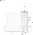
- FIG. 3 is a cross-sectional view of a first substrate or a first region of a substrate according to an embodiment
- FIG. 4 is a cross-sectional view of a first substrate or a first region of a substrate according to a comparative example
- FIGS. 5A to 5D are views illustrating a process of coupling a first adhesive member and a first reinforcing plate to a first substrate or a first region of a substrate according to an embodiment.
- the first substrate 801 or the first region 801 of the substrate 800 includes a first insulating layer 91-5.
- the first insulating layer 91-5 may mean an insulating layer disposed on a lowermost side among a plurality of insulating layers constituting the first substrate 801 or the first region 801 of the substrate 800.
- the first substrate 801 or the first region 801 of the substrate 800 may include a first ground pattern 82-6 disposed on a lower surface of the first insulating layer 91-5.
- the first ground pattern 82-6 may be formed of a plurality of layers.
- the first ground pattern 82-6 may have a structure in which a copper metal layer, a nickel metal layer, a palladium metal layer, and a gold metal layer are sequentially stacked, but is not limited thereto.
- a first cover layer 81b may be formed on a lower surface of the first insulating layer 91-5 of the first substrate 801 or the first region 801 of the substrate 800.
- the first cover layer 81b may be disposed on a lower surface of the first insulating layer 91-5 while covering at least a portion of the first ground pattern 82-6.
- the first cover layer 81b may include a first opening 32 exposing at least a portion of a lower surface of the first ground pattern 82-6.
- the first opening 32 may be substantially referred to as an opening.
- the first opening 32 of the first cover layer 81b includes a plurality of openings partially exposing the lower surface of the first ground pattern 82-6. That is, the first opening 32 of the first cover layer 81b may include a plurality of openings having a first width W1 and spaced apart from each other by a first distance D1.
- the first width W1 may be 0.1 mm to 0.5 mm, but is not limited thereto.
- the first width W1 is smaller than 0.1 mm, an overlapping area between the first ground pattern 82-6, the first adhesive member 83-1, and the first reinforcing plate 85-1 is reduced, so the effect of blocking EMI and improving RF sensitivity may be insufficient.
- a first distance D1 between centers of each of the plurality of openings constituting the first opening 32 of the first cover layer 81b may be 0.8 mm to 1.2 mm.
- the first distance D1 when the first distance D1 is smaller than the above range, it may have insufficient EMI blocking and RF sensitivity improvement effects corresponding to the decrease in the first width W1.
- the first distance D1 when the first distance D1 is greater than the above range, it may have insufficient EMI blocking and RF sensitivity improvement effects corresponding to the decrease in the first width W1.
- the plurality of openings constituting the first opening 32 may have a circular shape, but is not limited thereto.
- the plurality of openings may have any one of a rectangular shape, an elliptical shape, and a triangular shape.
- the first opening 32 of the embodiment does not include one large-area opening that entirely opens the first ground pattern 82-6 disposed on the lower surface of the first insulating layer 91-5, and the first opening 32 of the embodiment may include a plurality of small-area openings for partially exposing the first ground pattern 82-6.
- each of the plurality of openings of the small-area may be spaced apart from each other with a spacing in a range of 0.8 mm to 1.2 mm, and may have a width in a range of 0.1 mm to 0.5 mm.
- an area of the first ground pattern 82-6 in the embodiment may be greater than that of the first opening 32.
- the first ground pattern 82-6 includes a portion covered through the first cover layer 81b and a portion exposed through the first opening 32.
- an area of a portion covered through the first cover layer 81b may be greater than an area of a portion exposed through the first opening 32.
- a first adhesive member 83-1 is disposed under the lower surface of the first cover layer 81b.
- the first adhesive member 83-1 may be disposed under the lower surface of the first cover layer 81b while filling the first opening 32 formed in the first cover layer 81b.
- a thickness of the first portion of the first adhesive member 83-1 may be different from a thickness of the second portion.
- a thickness of the first portion of the first adhesive member 83-1 may be smaller than a thickness of the second portion.
- a thickness of the second portion of the first adhesive member 83-1 may correspond to a sum of a depth of the first opening 32 and a thickness of the first portion.
- the first adhesive member 83-1 and the first cover layer 81b had a peel strength of 1.1 kgF/cm before reflow and a peel strength of 1.12 kgF/cm after reflow.
- the first adhesive member 83-1 and the first ground pattern 82-6 have a peel strength of 0.93 kgF/cm, and a peel strength of 0.8 kgF/cm after reflow.
- the upper surface of the second portion of the first adhesive member 83-1 directly contacts the first ground pattern 82-6, and the lower surface is in direct contact with the first reinforcing plate 85-1, and accordingly it can connect the first reinforcing plate 85-1 and the first ground pattern 82-6 to each other.
- bending of the substrate 800 may occur according to a shape of the first opening 32 of the first cover layer 81b.
- the embodiment allows the first opening 32 to have a plurality of small-area openings partially exposing the first ground pattern 82-6, so that the entire region of the first region 801 of the first substrate 800 is pressed when the first reinforcing plate 85-1 is pressed, and so that bending of the substrate 800 can be minimized.
- the embodiment can maintain the flatness of the image sensor disposed on the substrate 800 by minimizing bending of the substrate 800, thereby improving reliability.
- a method of manufacturing the substrate, a process of coupling the first adhesive member, and a process of coupling the first reinforcing plate are as follows.
- the embodiment proceeds with a process of laminating the first cover layer 81b on the first insulating layer 91-5 and the first ground pattern 82-6 as described above and may manufacture the first region 801 of the substrate 800 as shown in FIG. 5B .
- the first cover layer 81b includes a first opening 32 having a plurality of openings that partially expose the first ground pattern 82-6 without exposing the entirety thereof.
- the first opening 32 of the first cover layer 81b includes a plurality of openings partially exposing a lower surface of the first ground pattern 82-6. That is, the first opening 32 of the first cover layer 81b may have a first width W1 and may include a plurality of openings in which centers thereof are spaced apart by a first distance D1. In this case, the first width W1 may be 0.1 mm to 0.5 mm, but is not limited thereto. When the first width W1 is smaller than 0.1 mm, an overlapping area between the first ground pattern 82-6, the first adhesive member 83-1, and the first reinforcing plate 85-1 is reduced, so the effect of blocking EMI and improving RF sensitivity may be insufficient.
- the embodiment may proceed with a process of disposing a first adhesive member 83-1 on the first cover layer 81b as shown in FIG. 5C .
- the first adhesive member 83-1 may also be disposed in the first opening 32 of the first cover layer 81b.
- the first adhesive member 83-1 may include a first portion disposed under the lower surface of the first cover layer 81b and a second portion disposed in the first opening 32.
- a thickness of the first portion of the first adhesive member 83-1 may be different from a thickness of the second portion.
- a thickness of the first portion of the first adhesive member 83-1 may be smaller than a thickness of the second portion.
- a thickness of the second portion of the first adhesive member 83-1 may correspond to a sum of a depth of the first opening 32 and a thickness of the first portion.
- the upper surface of the first portion of the first adhesive member 83-1 is in contact with the lower surface of the first cover layer 81b, and the upper surface of the second portion of the first adhesive member 83-1 is in contact with the lower surface of the ground pattern 82-6.
- an area of the first portion of the first adhesive member 83-1 may be greater than an area of the second portion of the first adhesive member 83-1.
- an area of a region in contact with the first cover layer 81b among an entire region of the upper surface of the first adhesive member 83-1 may be greater than an area in contact with the first ground pattern 82-6. Accordingly, the embodiment may improve the adhesive strength of the first adhesive member 83-1.
- the embodiment presses while the first reinforcing plate 85-1 is placed on the first adhesive member 83-1, and may proceed with a process of attaching the first reinforcing plate 85-1 to the lower surface of the first region 801 of the substrate 800 by reflowing the first adhesive member 83-1 after pressing as shown in FIG. 5D .
- FIG. 6 is a cross-sectional view of a second region of a substrate in a first direction according to an embodiment
- FIG. 7 is a cross-sectional view of a second region of a substrate in a second direction according to an embodiment
- FIGS. 8A to 8D show a process of coupling a noise shielding unit, a second adhesive member, and a second reinforcing plate to a substrate.
- FIG. 6 is a cross-sectional view in a AB direction of FIG. 8D
- FIG. 7 is a cross-sectional view in a CD direction of FIG. 8D
- FIGS. 8A to 8D show bottom views of a second region 802 and a third region 803 of a substrate 800
- FIGS. 6 and 7 may be a cross-sectional view of FIG. 8D rotated 180 degrees.
- the embodiment forms the second opening 31 exposing the pattern layer 82-6 (or ground pattern) from the second surface of the second region 802 of the substrate 800.
- the pattern layer 82-6 may be referred to as a "second ground layer”.
- a shape of the second ground pattern exposed through the second opening 31 is not limited to the shape shown in FIG. 8A (eg, ' ⁇ ' shape), and may be of various polygonal shapes (eg, square, triangular, etc.) or circular.
- FIG. 8A there is a region that is not exposed by the second opening 31 in a lower left portion, and this may form another ground pattern (eg, "analog ground pattern") that is separated or spaced apart from the second ground pattern (or “digital ground pattern”) exposed through the second opening 31.
- another ground pattern eg, "analog ground pattern”
- an analog ground pattern may also be exposed through the second opening 31, and a first noise shielding unit 71 and a second adhesive member 83-2 may be disposed between the exposed analog ground pattern and the second reinforcing plate 85-2.
- a depth H of the second opening 31 may be the same as a thickness of the second cover layer 81b of the substrate 800.
- the depth H of the second opening 31 may be a distance of the lens of the lens driving unit 100 or the lens barrel 400 in the optical axis direction.
- the depth H may range from 21 ⁇ m to 24 ⁇ m.
- the depth H may be 23 ⁇ m.
- the first noise shielding unit 71 may include a first portion 71a disposed in the second opening 31 of the second region 802 of the substrate 800, and a second portion 71b disposed under the third region 803 of the substrate 800.
- the first noise shielding unit 71 may include a third portion connecting the first portion and the second portion.
- the second portion 71b of the first noise shielding unit 71 may be disposed on a connection substrate 803, and an end of the first portion 71a may be disposed in the second opening 31 of the second substrate 802. For example, a portion of an end of the first portion 71a may be disposed in the second opening 31.
- the first portion 71a of the first noise shielding unit 71 may be disposed below the second ground pattern 82-6 of the second region 802 of the substrate 800 exposed by the second opening 31.
- a lower surface of the second opening 31 may be one surface (eg, the lower surface) of the exposed second ground pattern 82-6 of the second region 802 of the substrate 800.
- a lower surface of the first portion 71a of the first noise shielding unit 71 may contact a lower surface of the second opening 31.
- the first portion 71a of the first noise shielding unit 71 may include a first surface 21a (or “first side surface”) facing the first inner surface 31a of the second opening 31, a second surface 21b (or “second side surface”) facing the second inner surface 31b of the second opening 31, and a third surface 21c (or “third side surface”) facing the third inner surface 31c of the second opening 31.
- a side surface of the first portion 71a of the first noise shielding unit 71 may be positioned in the second opening 31 of the second region 802 of the substrate 800, and may be spaced apart from the second surface 11b of the second region 802 of the substrate 800.
- a length of the second portion 71b of the first noise shielding unit 71 in the vertical direction may be greater than a length L3 of the first portion 71a in the vertical direction. This is to improve the EMI shielding effect in the third region 803 of the substrate 800.
- a length of a first long side positioned on one side of the second opening 31 of the second substrate 802 may be greater than a length of a second long side positioned on the other side of the second opening 31.
- the first long side and the second long side may face each other.
- a length of a first short side positioned on one side of the second opening 31 of the second substrate 802 may be greater than a length of a second short side positioned on the other side of the second opening 31.
- the first short side and the second short side may face each other.
- a length L3 of the first portion 71a of the first noise shielding unit 71 in the vertical direction is smaller than a length L1 of the second opening 31 of the substrate 800 in the vertical direction (L3 ⁇ L1 ).
- a length L4 of the first portion 71a of the first noise shielding unit 71 in a horizontal direction is smaller than a length L2 of the second opening 31 of the substrate 800 in the horizontal direction (L4 ⁇ L2 ).
- the vertical direction may be a direction perpendicular to a direction from the image sensor 810 toward the connector 840.
- the horizontal direction may be a CD direction of FIG. 8D or a x-axis direction of FIG. 1 perpendicular to the optical axis direction of the lens driving unit 100.
- an area of the lower surface (or upper surface) of the first portion 71a of the first noise shielding unit 71 disposed within the second opening 31 of the substrate 800 may be smaller than an area of a lower surface of the second opening 31 of the substrate 800 (or an area of a lower surface of the exposed pattern layer 82-6).
- d4 may be greater than d3 (d4 > d3).
- d3 may be 0.6 mm to 0.8 mm
- d4 may be 0.9 mm to 1.1 mm.
- d4 d3 or d4 ⁇ d3.
- the first to third surfaces 21a to 21c of the first portion 71a of the first noise shielding unit 71 may be spaced apart from the first to third inner surfaces 31a to 31c of the second opening 31 of the substrate 800.
- the first surface 21a is spaced apart from the first inner surface 31a of the second opening 31
- the second surface 21b is spaced apart from the second inner surface 31b of the second opening 31
- the third surface 21c may be spaced apart from the third inner surface 31c of the second opening 31.
- a separation distance between the inner surfaces 31a to 31d of the second opening 31 and an end (eg, 21a to 21c) of the first noise shielding unit 71 may be greater than a separation distance between the inner surfaces 31a to 31d of the second opening 31 and an end of the second adhesive member 83-2. This is to improve adhesion between the second reinforcing plate 85-2 and the second substrate 802 by increasing the area of the second adhesive member 83-2.
- a horizontal (or vertical) separation distance between the inner surfaces 31a to 31d of the second opening 31 and an end of the second reinforcing plate 85-2 may be greater than a horizontal (or vertical) separation distance between the inner surfaces 31a to 31d of the second opening 31 and an end (eg, 21a to 21c) of the first noise shielding unit 71.
- the former may be equal to or smaller than the latter in other embodiments.
- the second adhesive member 83-2 may be a conductive adhesive member or may include a conductive adhesive member (eg, a conductive particle).
- the second adhesive member 83-2 may be FGBF-700.
- a side surface of the second adhesive member 83-2 may be spaced apart from the second surface 11b of the second region 802 of the substrate 800.
- a length L5 of the second adhesive member 83-2 in the vertical direction is smaller than a length L1 of the second opening 31 of the substrate 800 in the vertical direction (L5 ⁇ L1).
- a length L6 of the second adhesive member 83-2 in the horizontal direction is smaller than a length L2 of the second opening 31 of the substrate 800 in the horizontal direction (L6 ⁇ L2).
- a length L5 of the second adhesive member 83-2 in the vertical direction may be greater than or equal to a length L3 of the first portion 71a of the first noise shielding unit 71 in the vertical direction.
- a difference between the length of the first portion 71a of the first noise shielding unit 71 in the horizontal direction and the length of the second opening 31 in the horizontal direction is very small, and accordingly, a process margin for disposing the first portion 71a of the first noise shielding unit 71 is insufficient, the first noise shielding unit 71 may be separated out of the second opening 31, and as a result, a resistance value between the second reinforcing plate 85-2 and the ground of the substrate 800 may increase to 1 ohm or more.
- an area of the first portion 71a of the first noise shielding unit 71 may be reduced so that the performance of blocking noise emitted from the camera module may be weakened, and accordingly, it may deteriorate the RF sensitivity of the optical device to which the camera module is mounted.
- a length of the second adhesive member 83-2 in the horizontal direction is greater than the length of the second opening 31 in the horizontal direction so that the second adhesive member 83-2 can be disposed on the lower surface of the second region 802 of the substrate 800 outside the second opening 31, and it may increase the resistance value between the second reinforcing plate 85-2 and the ground of the substrate 800 to 1 ohm or more.
- a thickness (T1, eg, a thickness of the first portion 71a) of the first noise shielding unit 71 may be smaller than a depth H of the second opening 31 of the substrate 800 (T1 ⁇ H).
- a thickness of the first noise shielding unit 71 may be a length of the first noise shielding unit 71 in the optical axis direction.
- a thickness of the first noise shielding unit 71 (T1, a thickness of the first portion 71a) may be 12 [ ⁇ m] to 18 [ ⁇ m].
- a side surface of the first portion 71a of the noise shielding unit 71 may be positioned farther than inner surfaces 31a to 31d of the second opening 31 based on the outer surfaces 5a to 5c of the second region 802 of the substrate 800.
- the outer surface of the second reinforcing plate 85-2 may be positioned closer to the outer surfaces 5a to 5c of the second region 802 of the substrate 800 than to the sidewalls 31a to 31d of the second opening 31 of the substrate 300.
- each of the first adhesive member 83-1 and the second adhesive member 83-2 according to the embodiment may include conductive particles (not shown). Accordingly, the first reinforcing plate 85-1 in the embodiment may be electrically connected to the first ground pattern 82-6 through the first adhesive member 83-1. In addition, the second reinforcing plate 85-2 may be electrically connected to the second ground pattern 82-6 and the noise shielding unit 710 through the second adhesive member 83-2.
- a thickness T3 of the second reinforcing plate 85-2 may be less than a total thickness of the substrate 800 and may be greater than a thickness of the flexible substrate 800-1 and a thickness of the second adhesive member 83-2.
- the second reinforcing plate 85-2 may have a thickness of 90 ⁇ m to 120 ⁇ m.
- a thickness T3 of the second reinforcing plate 85-2 may be greater than a thickness T1 of the first noise shielding unit 71 and a thickness T2 of the second adhesive member 83-2 (T3 > T1, T2).
- an upper surface of the second reinforcing plate 85-2 may contact the second surface 11b (or lower surface) of the second region 802 of the substrate 800.
- the upper surface of an edge of the second reinforcing plate 85-2 may be in contact with the second surface 11b (or lower surface) of the second region 802 of the substrate 800.
- the embodiment may allow the first noise shielding unit 71 to be disposed between the pattern layer 82-6 opened by the second opening 31 of the second region 802 of the substrate 800 and the second reinforcing plate 85-2, and accordingly, it may shield or reduce EMI noise emitted from the camera module 200.
- the first noise shielding unit 71 and the second adhesive member 83-2 are disposed in the second opening 31, and accordingly, it is possible to have a structure in which the first noise shielding unit 71 and the second adhesive member 83-2 adhere closely to the pattern layer 82-6 exposed by the second opening 31, and it reduces the electrical resistance between the pattern layer 82-6 of the substrate 800 used for ground and the second reinforcing plate 85-2, and accordingly, it may use the second reinforcing plate 85-2 as a ground for the substrate 800. That is, the embodiment may allow the electrical resistance value between the pattern layer 82-6 of the substrate 800 and the second reinforcing plate 85-2 to have less than 1 ohm.
- FIG. 9 is a perspective view of a camera module according to another embodiment.
- a camera module 200 includes a lens or lens barrel 400, a lens driving unit 100, an adhesive member 612, a filter 610, a holder 600, a substrate 800, an image sensor 810, a motion sensor 820, a controller 830, a connector 840, a noise shielding unit 70, a first adhesive member (not shown), a second adhesive member (not shown), a first reinforcing plate 85-1 and a second reinforcing plate 85-2.
- the same reference numerals as those in FIG. 1 denote the same configurations, and descriptions of the same configurations are omitted or simplified.
- the description of the noise shielding unit 70 described in FIG. 1 may be equally applicable to the description of the noise shielding unit 70 of FIG. 9
- the description of the first adhesive member 83-1 and the second adhesive member 83-2 of FIG. 1 may be equally applicable to the description of the first and second adhesive members (not shown) of FIG. 8
- the description of the reinforcing plate of FIG. 1 may be equally applied to the first reinforcing plate 85-1 and the second reinforcing plate 85-2 of FIG. 9 .
- the lens driving unit 100 may be a lens driving unit for AF or a lens driving unit for OIS.
- the lens driving unit for AF is capable of performing only an auto focus function
- the lens driving unit for OIS is capable of performing an auto focus function and an OIS (Optical Image Stabilizer) function.
- a driving signal (eg, driving current) may be provided to the coil, and the bobbin may be moved in an optical axis direction by electromagnetic force generated by an interaction between the coil and the magnet.
- the coil may be disposed on the housing and the magnet may be disposed on the bobbin.
- the lens drive unit for AF may further include a sensing magnet disposed on the bobbin, an AF position sensor disposed in the housing (e.g., a hall sensor), and a circuit board on which the AF position sensor is disposed and which is disposed or mounted on the housing and/or the base for driving AF feedback.
- the AF position sensor may be disposed on the bobbin and the sensing magnet may be disposed on the housing.
- the circuit board may be electrically connected to the coil and the AF position sensor, a driving signal may be provided to each of the coil and the AF position sensor through the circuit board, and an output of the AF position sensor may be transmitted to the circuit board.
- a camera module may include a housing coupled to the lens or lens barrel 400 instead of the lens driving device 100 of FIG. 1 and fixed to the lens or lens barrel 400, and the housing may be coupled or attached to the upper surface of a holder 600.
- the housing attached or fixed to the holder 600 may not be moved, and a position of the housing may be fixed while attached to the holder 600.
- the lens driving unit for OIS may include a housing, a bobbin disposed within the housing and for mounting a lens or lens barrel 400, a first coil disposed on the bobbin, a magnet disposed in the housing and facing the first coil, at least one upper elastic member coupled to an upper portion of the bobbin and an upper portion of the housing, at least one lower elastic member coupled to a lower portion of the bobbin and a lower portion of the housing, a second coil disposed below the bobbin (or/and housing), a circuit board disposed below the second coil, and a base disposed below the circuit board.
- the lens driving unit for OIS may further include a support member electrically connecting the circuit board and the upper elastic member and supporting the housing with respect to the base.
- Each of the first coil and the second coil may be electrically connected to the circuit board 250 and may receive a driving signal (driving current) from the circuit board.
- the upper elastic member may include a plurality of upper springs
- the support member may include support members connected to the upper springs
- the first coil may be electrically connected to the circuit board through the upper springs and the support member.
- the circuit board may include a plurality of terminals, and a part of the plurality of terminals may be electrically connected to each of the first coil and/or the second coil.
- the bobbin and the lens or lens barrel 400 coupled thereto can be moved in the optical axis direction by the electromagnetic force generated by the interaction between the first coil and the magnet, and as a result, the displacement of the bobbin in the optical axis direction is controlled so that AF driving may be implemented.
- the housing may be moved in a direction perpendicular to the optical axis by the electromagnetic force due to the interaction between the second coil and the magnet, and thus, hand shake correction or OIS driving may be implemented.
- the lens driving unit may further include a sensing magnet (not shown) disposed on the bobbin and an AF position sensor (eg, a hall sensor, not shown) disposed on the housing for AF feedback driving.
- the lens driving unit may further include a circuit board (not shown) disposed on the housing and/or the base and on which the AF position sensor is disposed or mounted.
- the AF position sensor may be disposed on the bobbin, and the sensing magnet may be disposed on the housing.
- the lens driving unit may further include a balancing magnet disposed on the bobbin to correspond to the sensing magnet.
- the AF position sensor may output an output signal according to a result of detecting a strength of a magnetic field of the sensing magnet according to a movement of the bobbin.
- the AF position sensor may be electrically connected to the circuit board through the upper elastic member (or lower elastic member) and/or the support member.
- the circuit board may provide a driving signal to the AF position sensor, and an output of the AF position sensor may be transmitted to the circuit board, and a controller 830 may sense or detect the displacement of the bobbin using the output of the AF position sensor.
- the holder 600 may be disposed under the lens driving unit 100 (eg, a base).
- the filter 610 is mounted on the holder 600, and the holder 600 may have a protrusion 500 on which the filter 610 is seated.
- the adhesive member 612 may couple or attach the lens driving unit 100 (eg, a base) to the holder 600.
- the adhesive member 6120 may also serve to prevent foreign substances from entering the lens driving unit 100.
- the adhesive member 612 may be a thermosetting adhesive member (eg, thermosetting epoxy) or an ultraviolet curable adhesive member (eg, ultraviolet curable epoxy).
- the filter 610 may serve to block light of a specific frequency band from light passing through the lens barrel 400 from being incident to the image sensor 810.
- the filter 610 may be an infrared cut filter, but is not limited thereto. In this case, the filter 610 may be disposed parallel to a x-y plane.
- the substrate 800 is disposed under the holder 600, and the image sensor 810 may be mounted on the substrate 600.
- the image sensor 810 is a part where light passing through the filter 610 is incident and an image including the light is formed.
- the substrate 800 may include various circuits, elements, controllers, etc. to convert an image formed by the image sensor 810 into an electrical signal and transmit it to an external device.
- the substrate 800 may be implemented as a substrate on which an image sensor may be mounted, a circuit pattern may be formed, and various elements may be coupled.
- the holder 600 may be referred to as a "sensor base”, and the substrate 800 may be referred to as a "circuit board”.
- some regions of the substrate 800 may be implemented to be included in the lens driving unit 100 or not included in the lens driving unit 100.
- the image sensor 810 may receive an image included in light incident through the lens driving unit 100 and convert the received image into an electrical signal.
- the filter 610 and the image sensor 810 may be spaced apart from each other so as to face each other in the optical axis direction.
- the motion sensor 820 is mounted on the substrate 800 and may be electrically connected to the controller 830 through a circuit pattern provided on the substrate 800.
- the motion sensor 820 outputs rotational angular velocity information caused by the movement of the camera module 200.
- the motion sensor 820 may be implemented as a 2-axis or 3-axis gyro sensor or an angular velocity sensor.
- the controller 830 is mounted on the substrate 800, may be electrically connected to the lens driving unit 100, and may provide a driving signal for driving the AF coil to the lens driving unit 100, a driving signal for driving the OIS coil, a driving signal for driving the AF position sensor, or/and a driving signal for driving an Optical Image Stabilization (OIS) position sensor.
- a driving signal for driving the AF coil to the lens driving unit 100
- a driving signal for driving the OIS coil a driving signal for driving the AF position sensor
- OIS Optical Image Stabilization
- the controller 830 may receive an output of an AF position sensor or/and an output of an OIS position sensor, may provide a driving signal for feedback AF driving to the AF coil using the output of the AF position sensor of the lens driving unit 100, and may provide a driving signal for feedback OIS driving to the OIS coil using the output of the OIS position sensor of the lens driving unit 100.
- the connector 840 is electrically connected to the substrate 800 and may include a port for electrically connecting to an external device.
- the lens driving unit 100 forms an image of an object in space by using the characteristics of light such as reflection, refraction, absorption, interference, and diffraction, and may be included in an optical instrument for the purpose of increasing visual acuity of the eye, recording and reproducing an image by a lens, or optical measurement, propagation or transmission of an image, and the like.
- the optical device according to the embodiment includes a mobile phone, a mobile phone, a smart phone, a portable smart device, a digital camera, a laptop computer, a digital broadcasting terminal, a personal digital assistant (PDA), and a portable multimedia player (PMP), and navigation, but is not limited thereto, and it is possible to use any device for taking images or photos.
- FIG. 10 shows a perspective view of a portable terminal 200A according to an embodiment
- FIG. 11 shows a configuration diagram of the portable terminal shown in FIG. 9 .
- a portable terminal (200A, hereinafter referred to as a "terminal") may include a body 850, a wireless communication unit 710, an A/V input unit 720, a sensing unit 740, an input/output unit 750, a memory unit 760, an interface unit 770, a control unit 780, and a power supply unit 790.
- the body 850 shown in FIG. 10 is in the form of a bar, but is not limited thereto, and there may be various structures such as a slide type, a folder type, a swing type, a swivel type, in which two or more sub-bodies are coupled to be movable relative to each other.
- the body 850 may include a case (casing, housing, cover, etc.) forming an exterior.
- the body 850 may be divided into a front case 851 and a rear case 852.
- Various electronic components of the terminal may be embedded in a space formed between the front case 851 and the rear case 852.
- the wireless communication unit 710 may include one or more modules that enable wireless communication between the terminal 200A and the wireless communication system or between the terminal 200A and the network in which the terminal 200A is located.
- the wireless communication unit 710 may include a broadcast reception module 711, a mobile communication module 712, a wireless internet module 713, a short-range communication module 714, and a location information module 715.
- the A/V (Audio/Video) input unit 720 is for inputting an audio signal or a video signal, and may include a camera 721 and a microphone 722 and the like.
- the camera 721 may include a camera module according to the embodiment shown in FIG. 1 or 9 .
- the sensing unit may detect a current state of the terminal 200A, such as an opening/closing state of the terminal 200A, a position of the terminal 200A, a presence or absence of user contact, an orientation of the terminal 200A, acceleration/deceleration of the terminal 200A, etc. and generate a sensing signal for controlling the operation of the terminal 200A.
- a current state of the terminal 200A such as an opening/closing state of the terminal 200A, a position of the terminal 200A, a presence or absence of user contact, an orientation of the terminal 200A, acceleration/deceleration of the terminal 200A, etc.
- a sensing signal for controlling the operation of the terminal 200A.
- the terminal 200A is in the form of a slide phone, it is possible to sense whether the slide phone is opened or closed.
- it is responsible for sensing functions related to whether the power supply unit 790 is supplied with power, whether the interface unit 770 is coupled to an external device, and the like.
- the input/output unit 750 is for generating input or output related to sight, hearing, or touch.
- the input/output unit 750 may generate input data for operation control of the terminal 200A, and may also display information processed by the terminal 200A.
- the input/output unit 750 may include a keypad unit 730, a display module 751, a sound output module 752, and a touch screen panel 753.
- the keypad unit 730 may generate input data in response to a keypad input.
- the display module 751 may include a plurality of pixels whose color changes according to an electrical signal.
- the display module 751 may include at least of a liquid crystal display, a thin film transistor-liquid crystal display, an organic light-emitting diode, a flexible display, three-dimensional display (3D display).
- the sound output module 752 may output audio data received from the wireless communication unit 710 in a call signal reception, a call mode, a recording mode, a voice recognition mode, or a broadcast reception mode, or the like; or audio data stored in the memory unit 760.
- the touch screen panel 753 may convert a change in capacitance generated due to a user's touch on a specific region of the touch screen into an electrical input signal.
- the memory unit 760 may store a program for processing and control of the controller 780, and may temporarily store input/output data (eg, phone book, message, audio, still image, photo, video, etc.).
- input/output data eg, phone book, message, audio, still image, photo, video, etc.
- the memory unit 760 may store an image captured by the camera 721, for example, a photo or a moving picture.
- the interface unit 770 serves as a passage for connecting with an external device connected to the terminal 200A.
- the interface unit 770 receives data from an external device, receives power and transmits it to each component inside the terminal 200A, or transmits data of the terminal 200A to an external device.
- the interface unit 770 may include a wired/wireless headset port, an external charger port, a wired/wireless data port, a memory card port, a port for connecting a device having an identification module, and an audio I/O (Input/Output) port, video I/O (Input/Output) port, and an earphone port, and the like.
- the controller may control the overall operation of the terminal 200A.
- the controller 780 may perform related control and processing for voice calls, data communications, video calls, and the like.
- the controller 780 may perform a pattern recognition process capable of recognizing a handwriting input or a drawing input performed on the touch screen as characters and images, respectively.
Applications Claiming Priority (2)
| Application Number | Priority Date | Filing Date | Title |
|---|---|---|---|
| KR1020200125716A KR20220042655A (ko) | 2020-09-28 | 2020-09-28 | 카메라 모듈 |
| PCT/KR2021/013244 WO2022065987A1 (ko) | 2020-09-28 | 2021-09-28 | 카메라 모듈 |
Publications (1)
| Publication Number | Publication Date |
|---|---|
| EP4221472A1 true EP4221472A1 (de) | 2023-08-02 |
Family
ID=80846790
Family Applications (1)
| Application Number | Title | Priority Date | Filing Date |
|---|---|---|---|
| EP21873015.8A Pending EP4221472A1 (de) | 2020-09-28 | 2021-09-28 | Kameramodul |
Country Status (6)
| Country | Link |
|---|---|
| US (1) | US20230371170A1 (de) |
| EP (1) | EP4221472A1 (de) |
| JP (1) | JP2023544563A (de) |
| KR (1) | KR20220042655A (de) |
| CN (1) | CN116326216A (de) |
| WO (1) | WO2022065987A1 (de) |
Family Cites Families (5)
| Publication number | Priority date | Publication date | Assignee | Title |
|---|---|---|---|---|
| JP6499925B2 (ja) * | 2015-06-02 | 2019-04-10 | タツタ電線株式会社 | フレキシブルプリント配線板、フレキシブルプリント配線板用補強部材、及びフレキシブルプリント基板 |
| KR20190115020A (ko) * | 2017-02-13 | 2019-10-10 | 타츠타 전선 주식회사 | 프린트 배선판 |
| JP6371460B1 (ja) * | 2017-12-06 | 2018-08-08 | タツタ電線株式会社 | 配線基板用補強板 |
| KR102550170B1 (ko) * | 2018-01-04 | 2023-07-03 | 삼성전기주식회사 | 인쇄회로기판 및 이를 포함하는 카메라 모듈 |
| KR102551188B1 (ko) * | 2018-06-26 | 2023-07-04 | 엘지이노텍 주식회사 | 카메라 모듈 및 이를 포함하는 광학 기기 |
-
2020
- 2020-09-28 KR KR1020200125716A patent/KR20220042655A/ko unknown
-
2021
- 2021-09-28 WO PCT/KR2021/013244 patent/WO2022065987A1/ko active Application Filing
- 2021-09-28 JP JP2023519505A patent/JP2023544563A/ja active Pending
- 2021-09-28 CN CN202180065911.0A patent/CN116326216A/zh active Pending
- 2021-09-28 US US18/246,612 patent/US20230371170A1/en active Pending
- 2021-09-28 EP EP21873015.8A patent/EP4221472A1/de active Pending
Also Published As
| Publication number | Publication date |
|---|---|
| US20230371170A1 (en) | 2023-11-16 |
| CN116326216A (zh) | 2023-06-23 |
| JP2023544563A (ja) | 2023-10-24 |
| KR20220042655A (ko) | 2022-04-05 |
| WO2022065987A1 (ko) | 2022-03-31 |
Similar Documents
| Publication | Publication Date | Title |
|---|---|---|
| KR102492626B1 (ko) | 카메라 모듈 및 이를 포함하는 광학 기기 | |
| EP3817355B1 (de) | Kameramodul und optische vorrichtung damit | |
| TW201830120A (zh) | 相機模組 | |
| EP4221472A1 (de) | Kameramodul | |
| KR20200114263A (ko) | 카메라 모듈 | |
| CN116888969A (zh) | 传感器驱动装置 | |
| KR20200114264A (ko) | 카메라 모듈 | |
| EP4207729A1 (de) | Kameramodul | |
| EP4203629A1 (de) | Kameramodul | |
| US20240064393A1 (en) | Camera module | |
| US20230314663A1 (en) | Protective sheet and camera module comprising same | |
| EP4270923A1 (de) | Kameramodul | |
| KR20230000346A (ko) | 카메라 모듈 및 이를 포함하는 광학기기 | |
| KR20230000350A (ko) | 카메라 모듈 및 이를 포함하는 광학기기 | |
| KR20220053881A (ko) | 카메라 모듈 및 이를 포함하는 광학기기 | |
| KR20220148002A (ko) | 카메라 모듈 및 이를 포함하는 광학기기 | |
| KR20230040823A (ko) | 카메라 모듈 및 이를 포함하는 광학기기 | |
| KR20230000359A (ko) | 회로기판, 카메라 모듈 및 이를 포함하는 광학기기 | |
| KR20230000354A (ko) | 카메라 모듈 및 이를 포함하는 광학기기 | |
| KR20230000361A (ko) | 보호 시트 및 이를 포함하는 카메라 모듈 |
Legal Events
| Date | Code | Title | Description |
|---|---|---|---|
| STAA | Information on the status of an ep patent application or granted ep patent |
Free format text: STATUS: THE INTERNATIONAL PUBLICATION HAS BEEN MADE |
|
| PUAI | Public reference made under article 153(3) epc to a published international application that has entered the european phase |
Free format text: ORIGINAL CODE: 0009012 |
|
| STAA | Information on the status of an ep patent application or granted ep patent |
Free format text: STATUS: REQUEST FOR EXAMINATION WAS MADE |
|
| 17P | Request for examination filed |
Effective date: 20230418 |
|
| AK | Designated contracting states |
Kind code of ref document: A1 Designated state(s): AL AT BE BG CH CY CZ DE DK EE ES FI FR GB GR HR HU IE IS IT LI LT LU LV MC MK MT NL NO PL PT RO RS SE SI SK SM TR |
|
| DAV | Request for validation of the european patent (deleted) | ||
| DAX | Request for extension of the european patent (deleted) |