EP4220963A2 - Diagnostic circuits and methods for analog-to-digital converters - Google Patents
Diagnostic circuits and methods for analog-to-digital converters Download PDFInfo
- Publication number
- EP4220963A2 EP4220963A2 EP22205937.0A EP22205937A EP4220963A2 EP 4220963 A2 EP4220963 A2 EP 4220963A2 EP 22205937 A EP22205937 A EP 22205937A EP 4220963 A2 EP4220963 A2 EP 4220963A2
- Authority
- EP
- European Patent Office
- Prior art keywords
- signal
- analog
- digital
- summation
- adc
- Prior art date
- Legal status (The legal status is an assumption and is not a legal conclusion. Google has not performed a legal analysis and makes no representation as to the accuracy of the status listed.)
- Pending
Links
- 238000000034 method Methods 0.000 title claims abstract description 35
- 230000008569 process Effects 0.000 claims abstract description 13
- 230000005291 magnetic effect Effects 0.000 claims description 94
- 238000012360 testing method Methods 0.000 claims description 86
- 238000012545 processing Methods 0.000 claims description 15
- 238000011084 recovery Methods 0.000 claims description 8
- 230000005294 ferromagnetic effect Effects 0.000 description 19
- 230000006870 function Effects 0.000 description 11
- 230000005381 magnetic domain Effects 0.000 description 7
- 230000007274 generation of a signal involved in cell-cell signaling Effects 0.000 description 6
- 238000006243 chemical reaction Methods 0.000 description 5
- 239000004020 conductor Substances 0.000 description 5
- 230000008878 coupling Effects 0.000 description 5
- 238000010168 coupling process Methods 0.000 description 5
- 238000005859 coupling reaction Methods 0.000 description 5
- 238000001914 filtration Methods 0.000 description 5
- 238000004519 manufacturing process Methods 0.000 description 5
- 239000000758 substrate Substances 0.000 description 5
- 230000005355 Hall effect Effects 0.000 description 4
- 238000010586 diagram Methods 0.000 description 4
- 230000035945 sensitivity Effects 0.000 description 4
- 230000005540 biological transmission Effects 0.000 description 3
- 238000013461 design Methods 0.000 description 3
- 238000002347 injection Methods 0.000 description 3
- 239000007924 injection Substances 0.000 description 3
- 230000004044 response Effects 0.000 description 3
- 239000004065 semiconductor Substances 0.000 description 3
- 238000013459 approach Methods 0.000 description 2
- 230000008901 benefit Effects 0.000 description 2
- 230000007547 defect Effects 0.000 description 2
- 229920005994 diacetyl cellulose Polymers 0.000 description 2
- WPYVAWXEWQSOGY-UHFFFAOYSA-N indium antimonide Chemical compound [Sb]#[In] WPYVAWXEWQSOGY-UHFFFAOYSA-N 0.000 description 2
- 239000000463 material Substances 0.000 description 2
- 238000012544 monitoring process Methods 0.000 description 2
- 238000013139 quantization Methods 0.000 description 2
- JBRZTFJDHDCESZ-UHFFFAOYSA-N AsGa Chemical compound [As]#[Ga] JBRZTFJDHDCESZ-UHFFFAOYSA-N 0.000 description 1
- XUIMIQQOPSSXEZ-UHFFFAOYSA-N Silicon Chemical compound [Si] XUIMIQQOPSSXEZ-UHFFFAOYSA-N 0.000 description 1
- 238000004891 communication Methods 0.000 description 1
- 230000001934 delay Effects 0.000 description 1
- 230000009977 dual effect Effects 0.000 description 1
- -1 e.g. Chemical compound 0.000 description 1
- 238000005516 engineering process Methods 0.000 description 1
- 229910052732 germanium Inorganic materials 0.000 description 1
- GNPVGFCGXDBREM-UHFFFAOYSA-N germanium atom Chemical compound [Ge] GNPVGFCGXDBREM-UHFFFAOYSA-N 0.000 description 1
- 150000002472 indium compounds Chemical class 0.000 description 1
- 229910052751 metal Inorganic materials 0.000 description 1
- 239000002184 metal Substances 0.000 description 1
- 238000000926 separation method Methods 0.000 description 1
- 229910052710 silicon Inorganic materials 0.000 description 1
- 239000010703 silicon Substances 0.000 description 1
- 230000007704 transition Effects 0.000 description 1
- 230000005641 tunneling Effects 0.000 description 1
Images


Classifications
-
- H—ELECTRICITY
- H03—ELECTRONIC CIRCUITRY
- H03M—CODING; DECODING; CODE CONVERSION IN GENERAL
- H03M1/00—Analogue/digital conversion; Digital/analogue conversion
- H03M1/12—Analogue/digital converters
- H03M1/18—Automatic control for modifying the range of signals the converter can handle, e.g. gain ranging
- H03M1/188—Multi-path, i.e. having a separate analogue/digital converter for each possible range
-
- H—ELECTRICITY
- H03—ELECTRONIC CIRCUITRY
- H03M—CODING; DECODING; CODE CONVERSION IN GENERAL
- H03M1/00—Analogue/digital conversion; Digital/analogue conversion
- H03M1/10—Calibration or testing
- H03M1/1071—Measuring or testing
-
- G—PHYSICS
- G01—MEASURING; TESTING
- G01R—MEASURING ELECTRIC VARIABLES; MEASURING MAGNETIC VARIABLES
- G01R33/00—Arrangements or instruments for measuring magnetic variables
- G01R33/0023—Electronic aspects, e.g. circuits for stimulation, evaluation, control; Treating the measured signals; calibration
- G01R33/0029—Treating the measured signals, e.g. removing offset or noise
-
- G—PHYSICS
- G01—MEASURING; TESTING
- G01R—MEASURING ELECTRIC VARIABLES; MEASURING MAGNETIC VARIABLES
- G01R33/00—Arrangements or instruments for measuring magnetic variables
- G01R33/0023—Electronic aspects, e.g. circuits for stimulation, evaluation, control; Treating the measured signals; calibration
- G01R33/0041—Electronic aspects, e.g. circuits for stimulation, evaluation, control; Treating the measured signals; calibration using feed-back or modulation techniques
-
- G—PHYSICS
- G01—MEASURING; TESTING
- G01R—MEASURING ELECTRIC VARIABLES; MEASURING MAGNETIC VARIABLES
- G01R33/00—Arrangements or instruments for measuring magnetic variables
- G01R33/02—Measuring direction or magnitude of magnetic fields or magnetic flux
- G01R33/06—Measuring direction or magnitude of magnetic fields or magnetic flux using galvano-magnetic devices
-
- H—ELECTRICITY
- H03—ELECTRONIC CIRCUITRY
- H03M—CODING; DECODING; CODE CONVERSION IN GENERAL
- H03M1/00—Analogue/digital conversion; Digital/analogue conversion
- H03M1/10—Calibration or testing
- H03M1/1071—Measuring or testing
- H03M1/109—Measuring or testing for dc performance, i.e. static testing
-
- H—ELECTRICITY
- H03—ELECTRONIC CIRCUITRY
- H03M—CODING; DECODING; CODE CONVERSION IN GENERAL
- H03M1/00—Analogue/digital conversion; Digital/analogue conversion
- H03M1/12—Analogue/digital converters
- H03M1/124—Sampling or signal conditioning arrangements specially adapted for A/D converters
- H03M1/1245—Details of sampling arrangements or methods
-
- H—ELECTRICITY
- H03—ELECTRONIC CIRCUITRY
- H03M—CODING; DECODING; CODE CONVERSION IN GENERAL
- H03M1/00—Analogue/digital conversion; Digital/analogue conversion
- H03M1/12—Analogue/digital converters
- H03M1/124—Sampling or signal conditioning arrangements specially adapted for A/D converters
- H03M1/129—Means for adapting the input signal to the range the converter can handle, e.g. limiting, pre-scaling ; Out-of-range indication
- H03M1/1295—Clamping, i.e. adjusting the DC level of the input signal to a predetermined value
-
- H—ELECTRICITY
- H03—ELECTRONIC CIRCUITRY
- H03M—CODING; DECODING; CODE CONVERSION IN GENERAL
- H03M1/00—Analogue/digital conversion; Digital/analogue conversion
- H03M1/12—Analogue/digital converters
- H03M1/18—Automatic control for modifying the range of signals the converter can handle, e.g. gain ranging
- H03M1/181—Automatic control for modifying the range of signals the converter can handle, e.g. gain ranging in feedback mode, i.e. by determining the range to be selected from one or more previous digital output values
-
- H—ELECTRICITY
- H03—ELECTRONIC CIRCUITRY
- H03M—CODING; DECODING; CODE CONVERSION IN GENERAL
- H03M3/00—Conversion of analogue values to or from differential modulation
- H03M3/30—Delta-sigma modulation
- H03M3/378—Testing
-
- H—ELECTRICITY
- H03—ELECTRONIC CIRCUITRY
- H03M—CODING; DECODING; CODE CONVERSION IN GENERAL
- H03M1/00—Analogue/digital conversion; Digital/analogue conversion
- H03M1/06—Continuously compensating for, or preventing, undesired influence of physical parameters
- H03M1/0617—Continuously compensating for, or preventing, undesired influence of physical parameters characterised by the use of methods or means not specific to a particular type of detrimental influence
- H03M1/0619—Continuously compensating for, or preventing, undesired influence of physical parameters characterised by the use of methods or means not specific to a particular type of detrimental influence by dividing out the errors, i.e. using a ratiometric arrangement
- H03M1/0621—Continuously compensating for, or preventing, undesired influence of physical parameters characterised by the use of methods or means not specific to a particular type of detrimental influence by dividing out the errors, i.e. using a ratiometric arrangement with auxiliary conversion of a value corresponding to the physical parameter(s) to be compensated for
Definitions
- This disclosure relates generally to analog-to-digital converters (ADCs) and, more particularly, to diagnostic circuits and methods for ADCs.
- ADCs analog-to-digital converters
- sensors are used to perform various functions in a variety of applications.
- Some sensors include one or magnetic field sensing elements, such as a Hall effect element or a magnetoresistive element, to detect aspects of movement of a ferromagnetic article, or target, such as proximity, speed, and direction.
- a magnetic switch or "proximity detector” that senses the proximity of a ferromagnetic article
- a proximity detector that senses passing ferromagnetic articles (for example, magnetic domains of a ring magnet or gear teeth)
- a magnetic field sensor that senses a magnetic field density of a magnetic field
- a current sensor that senses a magnetic field generated by a current flowing in a current conductor
- an angle sensor that senses an angle of a magnetic field.
- Magnetic field sensors are widely used in automobile control systems, for example, to detect ignition timing from a position of an engine crankshaft and/or camshaft, and to detect a position and/or rotation of an automobile wheel for anti-lock braking systems.
- ADCs are widely used to convert analog signals into digital signals.
- Various types of ADCs are used, including sigma delta converters and successive approximation converters as examples.
- sensors and their components such as ADCs sometimes experience failures. These failures may be due to manufacturing defects, design defects, latent failures, or a combination of both as examples.
- Sensor integrated circuits are widely used in automobile control systems and other safety critical applications. There are a variety of specifications that set forth requirements related to permissible sensor quality levels, failure rates, and overall functional safety. For example, some automotive applications require conformity to Automotive Safety Integrity Level (ASIL) standards.
- ASIL Automotive Safety Integrity Level
- One approach to meeting such mandates has been to use redundant, identical circuits in a sensor integrated circuit.
- Another approach is to test parts during and after the manufacturing process. For example, some parts include self-test capabilities, i.e., internal circuitry that can be used by the part to test itself. These self-tests may include built-in self-tests (i.e., "BIST" tests) and can be used to test various aspect of the sensor circuitry.
- Described herein are circuits and methods for performing diagnostics on one or more ADCs. Some configurations include comparison in the analog domain of one or more ADC input signals with one or more of the ADC input signals that have been digitally converted and converted back to the analog domain by a digital-to-analog converter (DAC). Other configurations include comparison in the digital domain of one or more ADC input signals that have been converted to the digital domain to the one or more ADC input signals that are converted into the digital domain by a different ADC. Still other configurations involve injecting a pilot, or test signal into one or more ADCs and then filtering in the digital domain to recover the test signal. Comparison of the recovered test signal to a predetermined threshold can be used to determine the operational status of the one or more ADCs. These arrangements function to monitor the operational status of the ADC(s).
- DAC digital-to-analog converter
- apparatus includes an ADC configured to convert an analog signal to a digital signal, a comparator having a first input responsive to the analog signal, a second input responsive to the digital signal, and an output at which a comparison signal is provided, and an output checker configured to process the comparison signal to generate a fault signal indicative of whether a fault has occurred in the ADC.
- the analog signal can include a first analog signal and the sensor can further include a digital-to-analog converter (DAC) configured to convert the digital signal to a second analog signal, and wherein the comparator is an analog comparator responsive to the first analog signal at the first input and the second analog signal at the second input.
- the digital signal can include a first digital signal and the sensor can further include a second ADC configured to convert the analog signal to a second digital signal, wherein the comparator is a digital comparator responsive to the first digital signal at the first input and the second digital signal at the second input.
- apparatus including a first ADC configured to convert a first analog signal to a first digital signal, a second ADC configured to convert a second analog signal to a second digital signal, and an analog summation circuit responsive to the first analog signal and the second analog signal and configured to generate an analog summation signal as a sum of the first analog signal and the second analog signal.
- the apparatus further includes a digital summation circuit responsive to the first digital signal and the second digital signal and configured to generate a digital summation signal as a sum of the first digital signal and the second digital signal and a comparator having a first input responsive to the analog summation signal, a second input responsive to the digital summation signal, and an output at which a comparison signal is provided.
- the apparatus may further include an output checker configured to process the comparison signal to generate a fault signal indicative of whether a fault has occurred in one or both of the first ADC or the second ADC.
- the analog summation signal can include a first analog summation signal and the sensor can further include a digital-to-analog converter (DAC) configured to convert the digital summation signal to a second analog summation signal, wherein the comparator is an analog comparator responsive to the first analog summation signal at the first input and the second analog summation signal at the second input.
- the apparatus may further include a margin unit configured to adjust one or both of the first analog summation signal and the second analog summation signal.
- the digital summation signal may include a first digital summation signal and the sensor further include a third ADC configured to convert the analog summation signal to a second digital summation signal, wherein the comparator is a digital comparator responsive to the first digital summation signal at the first input and the second digital summation signal at the second input.
- the apparatus may further include a margin unit configured to adjust one or both of the first digital summation signal and the second digital summation signal.
- the first ADC, the second ADC, the analog summation circuit, the digital summation circuit, and the comparator can be part of a sensor configured to sense a parameter.
- the sensor can be a magnetic field sensor and can further include a first magnetic field sensing element configured to generate the first analog signal and a second magnetic field sensing element configured to generate the second analog signal.
- the apparatus can further include a first front end amplifier coupled to receive an output signal of the first magnetic field sensing element and configured to generate the first analog signal and a second front end amplifier coupled to receive an output signal of the second magnetic field sensing element and configured to generate the second analog signal.
- the first front end amplifier can include a first output at which the first analog signal is provided and a second output at which a copy of the first analog output signal is provided, wherein the analog summation circuit is coupled to receive the copy of the first analog output signal and wherein the second front end amplifier comprises a first output at which the second analog signal is provided and a second output at which a copy of the second analog output signal is provided, wherein the analog summation circuit is coupled to receive the copy of the second analog output signal.
- the first front end amplifier can be a chopper amplifier and the second front end amplifier can be a chopper amplifier.
- Each of the first ADC and the second ADC can include a Continuous Time Sigma Delta Modulator (CTSDM).
- CTSDM Continuous Time Sigma Delta Modulator
- a method includes converting a first analog signal to a first digital signal, converting a second analog signal to a second digital signal, generating an analog summation signal as a sum of the first analog signal and the second analog signal, generating a digital summation signal as a sum of the first digital signal and the second digital signal, and comparing a first signal based on the analog summation signal to a second signal based on the digital summation signal to generate a comparison signal.
- the method may include processing the comparison signal to determine whether a fault has occurred in one or both of the first ADC or the second ADC.
- the analog summation signal can include a first analog summation signal, and the method further include converting the digital summation signal to a second analog summation signal and wherein comparing comprises comparing the first analog summation signal to the second analog summation signal.
- the method may further include adjusting one or both of the first analog summation signal or the second analog summation signal before comparing.
- the digital summation signal may include a first digital summation signal
- the method may further include converting the analog summation signal to a second dial summation signal and wherein comparing comprises comparing the first digital summation signal to the second digital summation signal.
- the method can include adjusting one or both of the first digital summation signal and the second digital summation signal.
- apparatus including a sensing element configured to generate an analog input signal indicative of a parameter to be sensed, an offset cancellation circuit coupled to receive the analog input signal and configured to remove an offset associated with the analog input signal, a test circuit coupled to receive the analog input signal and configured to combine a test signal with the analog input signal to generate a combined signal, wherein the test circuit is substantially identical to the offset cancellation circuit, an ADC having an input coupled to receive the combined signal and an output at which a digital signal corresponding to the analog input signal is provided, a recovery circuit configured to process the digital signal to recover the test signal, and a checker circuit configured to determine if an error has occurred in the ADC based on the recovered test signal.
- the recovery circuit can include a bandpass filter.
- the checker circuit can include a comparator configured to compare the recovered test signal to a predetermined threshold.
- Each of the offset cancellation circuit and the test circuit can include a DAC configured to receive a digital control signal, at least one current source element controllable to add a current to the digital signal, at least one current sink element controllable to subtract a current from the digital signal, and a binary control signal configured to selectively enable or disable the at least one current source element and the at least one current sink element.
- the apparatus can further include a linearity checker circuit configured to adjust the digital control signal and compare the recovered test signal to an adjusted predetermined threshold.
- the sensing element can include a magnetic field sensing element.
- the offset cancellation circuit can be configured to remove the offset associated with the analog input signal during a first time period and wherein the test circuit is configured to combine the test signal with the analog input signal during a second time period that does not overlap with the first time period.
- magnetic field sensing element is used to describe a variety of electronic elements that can sense a magnetic field.
- the magnetic field sensing element can be, but is not limited to, a Hall effect element, a magnetoresistance element, or a magnetotransistor.
- Hall effect elements for example, a planar Hall element, a vertical Hall element, and a Circular Vertical Hall (CVH) element.
- magnetoresistance elements for example, a semiconductor magnetoresistance element such as Indium Antimonide (InSb), a giant magnetoresistance (GMR) element, for example, a spin valve, an anisotropic magnetoresistance element (AMR), a tunneling magnetoresistance (TMR) element, and a magnetic tunnel junction (MTJ).
- the magnetic field sensing element may be a single element or, alternatively, may include two or more magnetic field sensing elements arranged in various configurations, e.g., a half bridge or full (Wheatstone) bridge.
- the magnetic field sensing element may be a device made of a type IV semiconductor material such as Silicon (Si) or Germanium (Ge), or a type III-V semiconductor material like Gallium-Arsenide (GaAs) or an Indium compound, e.g., Indium-Antimonide (InSb).
- a type IV semiconductor material such as Silicon (Si) or Germanium (Ge)
- a type III-V semiconductor material like Gallium-Arsenide (GaAs) or an Indium compound, e.g., Indium-Antimonide (InSb).
- some of the above-described magnetic field sensing elements tend to have an axis of maximum sensitivity parallel to a substrate or in the plane of the substrate that supports the magnetic field sensing element, and others of the above-described magnetic field sensing elements tend to have an axis of maximum sensitivity perpendicular to a substrate that supports the magnetic field sensing element.
- planar Hall elements tend to have axes of maximum sensitivity perpendicular to a substrate
- metal based or metallic magnetoresistance elements e.g., GMR, TMR, AMR
- vertical Hall elements tend to have axes of maximum sensitivity parallel to a substrate.
- magnetic field signal is used to describe any signal that results from a magnetic field experienced by a magnetic field sensing element.
- magnetic field sensor or simply “sensor” is used to describe a circuit that uses one or more magnetic field sensing elements, generally in combination with other circuits.
- the magnetic field sensor can be, for example, a rotation detector, a movement detector, a current sensor, or a proximity detector.
- a rotation detector can sense rotation of an object, for example, advance and retreat of magnetic domains of a ring magnet or advance and retreat of gear teeth of a ferromagnetic gear.
- movement detector can be used to describe either a rotation detector or a magnetic field sensor that can sense different movement, e.g., linear movement, of a ferromagnetic object, for example, linear movement of magnetic domains of a ring magnet or linear movement of gear teeth of a ferromagnetic gear.
- Magnetic field sensors are used in a variety of applications, including, but not limited to an angle sensor that senses an angle of a direction of a magnetic field, a current sensor that senses a magnetic field generated by a current carried by a current-carrying conductor, a magnetic switch that senses the proximity of a ferromagnetic object, a rotation detector (or movement detector) that senses passing ferromagnetic articles, for example, magnetic domains of a ring magnet or a ferromagnetic target (e.g., gear teeth) where the magnetic field sensor is used in combination with a back-bias or other magnet, and a magnetic field sensor that senses a magnetic field density of a magnetic field.
- the circuits and techniques described herein apply to any magnetic field sensor capable of detecting a magnetic field.
- processors and “controller” are used to describe electronic circuitry that performs a function, an operation, or a sequence of operations.
- the function, operation, or sequence of operations can be hard coded into the electronic circuit or soft coded by way of instructions held in a memory device.
- the function, operation, or sequence of operations can be performed using digital values or using analog signals.
- the processor or controller can be embodied in an application specific integrated circuit (ASIC), which can be an analog ASIC or a digital ASIC, in a microprocessor with associated program memory and/or in a discrete electronic circuit, which can be analog or digital.
- a processor or controller can contain internal processors or modules that perform portions of the function, operation, or sequence of operations.
- a module can contain internal processors or internal modules that perform portions of the function, operation, or sequence of operations of the module.
- a so-called “comparator” can be comprised of an analog comparator having a two-state output signal indicative of an input signal being above or below a threshold level (or indicative of one input signal being above or below another input signal).
- the comparator can also be comprised of a digital circuit having an output signal with at least two states indicative of an input signal being above or below a threshold level (or indicative of one input signal being above or below another input signal), respectively, or a digital value above or below a digital threshold value (or another digital value), respectively.
- predetermined when referring to a value or signal, is used to refer to a value or signal that is set, or fixed, in the factory at the time of manufacture, or by external means, e.g., programming, thereafter.
- the term “determined,” when referring to a value or signal, is used to refer to a value or signal that is identified by a circuit during operation, after manufacture.
- a magnetic field sensor 10 includes an ADC 20a configured to convert an analog input signal 18a to a digital signal 50a, a comparator 100 having a first input responsive to the analog input signal 18a (and here responsive to a copy, or replica 22a of the analog input signal), a second input responsive to the digital signal 50a, and an output at which a comparison signal 104 is provided.
- a window checker 80 as may be designed to meet ASIL or other requirements, includes an output checker 88 configured to process the comparison signal 104 to generate a fault signal 90 indicative of whether a fault has occurred in the ADC 20a.
- Fault signal 90 can be provided to internal or external circuitry or systems according to application requirements. For example, an external system controller and/or user can be informed that the sensor has a failure. Further, an external system controller can respond to a fault signal indication of a faulty ADC by shutting down the sensor 10 or by putting the sensor into a safe state or safe mode of operation in which portions of the sensor are disabled, thereby reducing power consumption.
- the analog input signal 18a is generated by one or more magnetic field sensing elements 12a, which sensing elements generate a magnetic field signal 14a indicative of a sensed magnetic field.
- the sensed magnetic field can be affected by movement (e.g., rotation) of a target as may take a variety of forms, including, but not limited to a gear having gear teeth or a ring magnet having one or more pole pair.
- movement e.g., rotation
- a target e.g., a gear having gear teeth or a ring magnet having one or more pole pair.
- linear arrangements of ferromagnetic objects that move linearly are possible.
- a permanent magnet can be placed at a variety of positions proximate to the target, resulting in fluctuations of the magnetic field as the gear rotates in a so-called "back-bias" arrangement.
- Sensing elements 12a can take a variety of forms, such as Hall effect elements or MR elements as non-limiting examples.
- the magnetic field signal can be amplified by a front-end amplifier 16a.
- amplifier 16a generates the output signal 18a in the form of an output current (e.g., Io_ch1).
- replica output signal 22a can be provided by the amplifier 16a for diagnostic processing, so that the main signal path (i.e., from signal 18a to sensor output signal 72) is not affected by the diagnostic processing.
- amplifier 16a is a so-called chopped amplifier with which offsets and low frequency noise can be reduced.
- amplifier 16a can include a switch, or modulator that modulates signal 14a at a chopping frequency. Chopping of the magnetic field signal 14a causes signal 18a to be shifted to a frequency related to the chopping frequency (e.g., fchop).
- a demodulator (not shown) is provided to demodulate the chopped amplifier output signal in order to recover the signal modulated by the chopped amplifier 16a.
- the magnetic field sensor 10 can include more than the one ADC 20a and, according to FIG. 1 , can include anywhere from one to "n" ADCs 20a - 20n, where n can be two or greater.
- Each of the "n" ADCs 20a - 20n is configured to convert a respective analog input signal 18a - 18n to a digital signal 50a - 50n, as shown.
- Analog input signals 18a - 18n can be generated by a front-end amplifier 16a - 16n in response to a magnetic field signal 14a - 14n generated by one or more magnetic field sensing elements 12a - 12n, respectively, as shown.
- the sensor 10 includes an analog summation circuit 24 responsive to the analog replica signals 22a - 22n and configured to generate an analog summation signal 26 as a sum of the signals 22a - 22n.
- the sensor 10 includes a digital summation circuit 74 responsive to the digital signals 50a - 50n from the ADCs 20a - 20n, respectively, and configured to generate a digital summation signal 76 as a sum of the digital signals.
- Comparator 100 has a first input responsive to the analog summation signal 26 (in the form of a signal 92), a second input responsive to the digital summation signal 76 (in the form of a signal 98), and an output at which the comparison signal 104 is provided.
- the output checker 88 is configured to process the comparison signal 104 to generate a fault signal 90 indicative of whether a fault has occurred in any of the ADCs 20a - 20n.
- the ADCs 20a - 20n can take various forms, such as the illustrated Continuous Time Sigma Delta Modulators (CTSDMs).
- CTSDM ADCs each ADC 20a - 20n can have a forward signal path including a summation element 30a - 30n, an integrator 34a - 34n, a second summation element 38a - 38n, a second integrator 42a - 42n, and an operational amplifier 46a - 46n.
- a feedback path of each CTSDM ADC 20a - 20n can include a DAC 48a - 48n generating a feedback signal for coupling to summation elements 30a - 30n and 38a - 38n, as shown.
- Conversion by the ADCs 20a - 20n includes filtering in the digital domain 60 by an associated digital filter 64a - 64n, as may take the form of a Cascaded Integrator Comb (CIC) filter in order to cancel quantization noise.
- Each CIC filter 64a - 64n generates a main signal path output signal 66a - 66n for coupling to a processor 70 and a replica output signal 68a - 68n for diagnostic processing. It will be appreciated by those of ordinary skill in the art that other types of ADCs are possible and will benefit from the diagnostic circuitry and techniques described herein.
- Processor 70 operates on the main signal path digital signals 66a - 66n in order to generate a sensor output signal 72 indicative of one or more parameters sensed by the magnetic field sensing elements 12a - 12n in a format tailored to meet application requirements.
- sensor 10 can be an angle sensor that senses an angle of a direction of a magnetic field, a current sensor that senses a magnetic field generated by a current carried by a conductor, a magnetic switch that senses proximity of a ferromagnetic object, a rotation detector (or movement or speed detector) that senses passing ferromagnetic articles, for example, magnetic domains of a ring magnet or a ferromagnetic target (e.g., gear teeth) where the magnetic field sensor is used in combination with a back-bias or other magnet, or a magnetic field sensor that senses a magnetic field density of a magnetic field, as non-limiting examples.
- Example sensor output signal formats include an Inter-Integrated Circuit (I 2 C) interface, a Controller Area Network (CAN) bus interface,
- the replica digital signals 68a - 68n are coupled to summation element 74 that is configured to generate the digital summation signal 76.
- the window checker 80 can include a margin unit 84 with which margin codes are combined (e.g., added and/or subtracted) from the digital summation signal 76 for comparison by comparator 100.
- An output signal 94 of the margin combiner 84 is converted to the analog domain by a DAC 96, as can take the form of an N-bit current DAC, to generate comparator input signal 98.
- the illustrated ADC diagnostics advantageously does not affect the main signal path with which the sensor output signal 72 is generated since the diagnostic comparison by comparator 100 is achieved in a dedicated diagnostic path using replica signals.
- a margin code is a digital word that is combined with the digital summation signal 76 so that the output checker 88 can reconcile the comparator output signal 104 in order to determine whether an ADC fault has occurred. For example, a first margin code can be added to the digital summation signal 76 at first times to generate comparator input signal 98 for comparison to the analog summation signal 26 in order to determine if the signal 98 is greater than the analog summation signal 26 as would be expected based on the addition of the margin code. If the signal 98 is greater than the signal 92, then the comparator output signal 104 can be at a first logic level that is processed by the output checker 88 to determine that the ADCs 20a - 20n are operating properly.
- the fault signal 90 indicates that the ADCs 20a - 20n are operating properly. If however the signal 98 is less than the signal 92, then the comparator output signal 104 can be at a second logic level that is processed by the output checker 88 to determine that one or more of the ADCs 20a - 20n is not operating properly and the fault signal 90 can be generated to so indicate the presence of an ADC fault.
- the fault in this scenario would indicate that output of one or more ADCs 20a - 20n is stuck low as the signal 98 remains below the analog summation signal 92 even when a margin code is added.
- a second margin code can be subtracted from the digital summation signal 76 at second times to generate comparator input signal 98 for comparison to the analog summation signal 26 in order to determine if the signal 98 is less than the analog summation signal 26 as would be expected based on the subtraction of the margin code. It will be appreciated by those of ordinary skill in the art that the second margin code can be the same as, or different than the first margin code. If the signal 98 is less than the signal 92, then the comparator output signal 104 can be at the first logic level that is processed by the output checker 88 to determine that the ADCs 20a - 20n are operating properly. In this scenario, the fault signal 90 indicates that the ADCs 20a - 20n are operating properly.
- the comparator output signal 104 can be at the second logic level that is processed by the output checker 88 to determine that one or more of the ADCs 20a - 20n is not operating properly and the fault signal 90 can be generated to so indicate the presence of an ADC fault.
- the fault in this scenario would indicate that output of one or more ADCs 20a - 20n is stuck high as the signal 98 remains above the analog summation signal 92 even when a margin code is added.
- Comparator 100 can be a current comparator and be configured to compare the input signal 92 to the input signal 98 in order to generate output signal 104, as shown.
- Input signal 92 can be a filtered version of the analog summation signal 26.
- a low pass filter 28 can filter the analog summation signal 26 and generate the comparator input signal 92, as shown.
- the low pass filter 28 adds a delay to the analog summation signal 26 which can reduce or eliminate errors due to the delay of the signal 98 relative to the analog summation signal 26. Additionally, the low pass filter 28 can cancel AC offset if the sensor 10 is chopped.
- first times when margin combiner 84 adds a margin code to the digital summation signal 76 and the second times when the margin combiner subtracts a margin code from the digital summation signal can be a continuous sequence of first and second time periods occurring at a rate selected to reliably detect ADC faults and tailored to the speed of the associated processing circuitry (e.g., comparator 100).
- sensor 10 could perform the described ADC diagnostics voltage signals rather than the analog current signals 18a - 18n, in which case generation of replica analog signals 22a - 22n and replica digital signals 68a - 68n could be omitted and the current comparator 100 could be a voltage comparator.
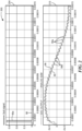
- Plot 204 illustrates the fault signal 90 and, in the illustrated embodiment, a logic low level of fault signal 90 can indicate the absence of an ADC fault or failure and a logic high level (e.g., of approximately 1volt) can indicate the presence of an ADC fault or failure.
- Plot 210 illustrates comparator input signals 92 and 98, with input signal 92 being indicative of the analog summation signal 26 (as may be filtered by filter 28) and input signal 98 being indicative of the digital summation signal 76 with margin codes added or subtracted by margin combiner 84 and having been brought back to the analog domain by DAC 96 as explained above.
- Plot 210 illustrates an operating condition in which there are no ADC faults present. This can be seen by the DAC output signal 98 and the analog summation signal 92 closely tracking one another. In other words, when margin codes are added to the digital summation signal 76 (e.g., at example times labeled 98a), the comparator output signal 104 is at a logic high level as is expected and when margin codes are subtracted from the digital summation signal (e.g., at example times labeled 98b), the comparator output signal 104 is at a logic low level as is expected.
- Output checker 88 interprets the comparator output signal 104 based the expected relationship between the compared signals 92, 98 given the addition or subtraction of margin codes.
- the DAC output signal 98 is greater than the analog summation signal 92 when margin codes are added to the digital summation signal 76 (i.e., at times labeled 98a)
- fault signal 90 is at a logic low level to indicate that no fault has been detected.
- DAC output signal 98 is less than the analog summation signal when margin codes are subtracted from the digital summation signal 76 (i.e., at times labeled 98b)
- fault signal 90 is at a logic low level to indicate that no fault has been detected.
- Example fault signal 90 has a single pulse 90a occurring shortly after power up of the sensor 10. This pulse 90a occurs because it takes time for the output 98 of DAC 96 to reach the level of the analog summation signal 92 due to signal processing delays. In general however, there is an initial power on time during which sensor 10 does not output signals 72, 90 so there is no communication of a false ADC error condition.
- Plot 304 illustrates the fault signal 90 (here again with a logic low level indicative of the absence of an ADC fault and a logic high level indicative of the presence of an ADC fault) and plot 310 illustrates the comparator input signals 92 and 98.
- plot 310 illustrates an operating condition in which an ADC fault occurs.
- the DAC output signal 98 drifts from its expected value of the analog summation signal 92.
- This fault condition can be described as one or more of the ADCs 20a - 20n being stuck high.
- the DAC output signal 98 and the analog summation signal 92 closely track one another such that when margin codes are added to the digital summation signal 76 (e.g., at example times labeled 98a), the comparator output signal 104 is at a logic high level as is expected and when margin codes are subtracted from the digital summation signal 76 (e.g., at example times labeled 98b), the comparator output signal 104 is at a logic low level as is expected.
- the DAC output signal 98 no longer tracks closely with the analog summation signal 92. Rather, when a margin code is added to the digital summation signal 76 (e.g., at example times labeled 98a'), the comparator output signal 104 is at a logic high level as is expected; however, when a margin code is subtracted from the digital summation signal (e.g., at example times labeled 98b'), the comparator output signal 104 is still at a logic low level and this is not the expected relationship between the comparator input signals under the condition of subtracting a margin code.
- a margin code is added to the digital summation signal 76 (e.g., at example times labeled 98a')
- the comparator output signal 104 is at a logic high level as is expected; however, when a margin code is subtracted from the digital summation signal (e.g., at example times labeled 98b'), the comparator output signal 104 is still at a logic low level and this is
- output checker 88 that is configured to interpret the comparator output signal 104 based on the expected relationship between the compared signals 92, 98 generates fault signal 90 having transitions to a logic high level to indicate the presence of a fault at times (e.g., 98b') when the comparator output signal is not at its expected level.
- an alternative sensor 400 includes one or more ADCs 420a - 420n, each configured to convert a respective analog input signal 418a - 418n into a digital signal 450a - 450n, a comparator 486 having a first input responsive to the analog input signals 418a - 418n (and here responsive to replicas 422a - 422n of the analog input signals), a second input responsive to the digital signals 450a - 450n, and an output at which a comparison signal 496 is provided.
- a window checker 480 includes an output checker 488 configured to process the comparison signal 496 to generate a fault signal 490 indicative of whether a fault has occurred in any of the ADCs 420a - 420n.
- Fault signal 490 can be provided to internal or external circuitry or systems according to application requirements.
- Sensor 400 is described herein as including more than one ADCs 420a - 420n (i.e., "n" is two or greater) and associated circuitry. However, it will be appreciated by those of ordinary skill in the art that sensor 400 can include a single ADC 420a, in which case summation elements 424 and 474 can be omitted.
- Analog input signals 418a - 418n can be generated by one or more magnetic field sensing elements 412a - 412n that generate magnetic field signals 414a - 414n for processing by front-end amplifiers 416a - 416n, respectively.
- amplifiers 416a - 416n generate output signals 418a - 418n in the form of an output current (e.g., Io_ch1)
- replica output signals 422a - 422n can be provided for diagnostic processing, so that the main signal path (i.e., from signals 418a - 418n to sensor output signal 472) is not affected by the diagnostic processing.
- Amplifiers 416a - 416n can be chopped amplifiers, in which case demodulators (not shown) are provided to demodulate the chopped amplifier output signals in order to recover the signal modulated by the chopped amplifiers 416a - 416n.
- An analog summation circuit 424 responsive to the analog replica signals 422a - 422n is configured to generate an analog summation signal 426 as a sum of the signals 422a - 422n.
- Sensor 400 differs from sensor 10 of FIG. 1 in that the comparison of the analog input signal(s) 422a - 422n to the converted digital signal(s) 450a - 450n is performed in the digital domain 460.
- sensor 400 includes an additional ADC 456 configured to convert the analog summation signal 426 into a digital signal 458.
- ADC 456 can be the same as or similar to ADCs 420a- 420n.
- ADC 456 can be a different type of ADC than ADCs 420a - 420n.
- ADC 456 can be a less accurate ADC (e.g., slower and/or providing lower resolution), but can be a lower cost ADC (e.g., in terms of area and/or power consumption).
- ADC 456 can take the form of a dual slope ADC.
- a scaler 428 can be provided to scale down the level of the analog summation signal 426 in order to preserve the dynamic range of the ADC 456.
- analog summation signal 426 can be scaled down by 1/n, where n is the number of ADCs 420a - 420n.
- a rescaler (not shown) can be provided in the digital domain 460 in order to increase the magnitude of the resulting signal for comparison.
- the digital version 458 of the analog summation signal 426 can be filtered by a filter 462 in the digital domain 460.
- conversion can include filtering by a CIC filter 462.
- the output signal 492 of filter 462 can thus be indicative of the summation of the analog replica signals 422a - 422 and can be coupled to comparator 486, as shown.
- the sensor 400 includes a digital summation circuit 474 responsive to the digital signals 450a - 450n from the ADCs 420a - 420n, respectively, and configured to generate a digital summation signal 476 as a sum of the digital signals.
- Comparator 486 thus is coupled to receive a first input signal 492 responsive to the analog summation signal 426 and a second input signal 498 responsive to the digital summation signal 476.
- a comparison signal 496 provided by the comparator 486 is coupled to an output checker 488 that is configured to process the comparison signal 496 to generate a fault signal 490 indicative of whether a fault has occurred in any of the ADCs 420a - 420n.
- the ADCs 420a - 420n can take various forms, such as the illustrated Continuous Time Sigma Delta Modulators (CTSDMs), each of which can have a forward signal path including a summation element 430a - 430n, an integrator 434a - 434n, a second summation element 438a - 438n, a second integrator 442a - 442n, and an operational amplifier 446a - 446n.
- a feedback path of each CTSDM ADC 420a - 420n can include a DAC 448a - 448n generating a feedback signal for coupling to summation elements 430a - 430n and 438a - 438n, as shown.
- Conversion by the ADCs 420a - 420n includes filtering in the digital domain 460 by an associated digital filter 464a - 464n, as may take the form of a Cascaded Integrator Comb (CIC) filter in order to cancel quantization noise.
- Each CIC filter 464a - 464n generates a main signal path output signal 466a - 466n for coupling to a processor 470 and a replica output signal 468a - 468n for diagnostic processing. It will be appreciated by those of ordinary skill in the art that other types of ADCs are possible and will benefit from the diagnostic circuitry and techniques described herein.
- Sensor 400 can be an angle sensor that senses an angle of a direction of a magnetic field, a current sensor that senses a magnetic field generated by a current carried by a conductor, a magnetic switch that senses proximity of a ferromagnetic object, a rotation detector (or movement or speed detector) that senses passing ferromagnetic articles, for example, magnetic domains of a ring magnet or a ferromagnetic target (e.g., gear teeth) where the magnetic field sensor is used in combination with a back-bias or other magnet, or a magnetic field sensor that senses a magnetic field density of a magnetic field, as non-limiting examples.
- Example sensor output signal formats include an Inter-Integrated Circuit (I 2 C) interface, a Controller Area Network (CAN) bus interface, a Single Edge Nibble Transmission (SENT) interface,
- the replica digital signals 468a - 468n are coupled to summation element 474 that is configured to generate the digital summation signal 476. It will be appreciated by those of ordinary skill in the art that the illustrated ADC diagnostics advantageously does not affect the main signal path with which the sensor output signal 472 is generated since the diagnostic comparison by comparator 400 is achieved in a dedicated diagnostic path using replica signals.
- the window checker 480 can include a margin unit 484 with which margin codes are combined (e.g., added and/or subtracted) from the digital summation signal 476 for comparison by comparator 486.
- An output signal 498 of the margin combiner 484 is coupled to comparator 486 as shown.
- a margin code is a digital word that is combined with the digital summation signal 476 so that the output checker 488 can reconcile the comparator output signal 496 in order to determine whether an ADC fault has occurred.
- a first margin code can be added to the digital summation signal 476 at first times to generate comparator input signal 498 for comparison to the analog summation signal 426 in order to determine if the signal 498 is greater than the analog summation signal 426 as would be expected based on the addition of the margin code. If the signal 498 is greater than the signal 492, then the comparator output signal 496 can be at a first logic level that is processed by the output checker 488 to determine that the ADCs 420a - 420n are operating properly. In this scenario, the fault signal 490 indicates that the ADCs 420a - 420n are operating properly.
- the comparator output signal 496 can be at a second logic level that is processed by the output checker 488 to determine that one or more of the ADCs 420a - 420n is not operating properly and the fault signal 490 can be generated to so indicate the presence of an ADC fault.
- the fault in this scenario would indicate that output of one or more ADCs 420a - 420n is stuck low as the signal 498 remains below the analog summation signal 492 even when a margin code is added.
- a second margin code can be subtracted from the digital summation signal 476 at second times to generate comparator input signal 498 for comparison to the analog summation signal 426 in order to determine if the signal 498 is less than the analog summation signal 426 as would be expected based on the subtraction of the margin code. It will be appreciated by those of ordinary skill in the art that the second margin code can be the same as, or different than the first margin code. If the signal 498 is less than the signal 492, then the comparator output signal 496 can be at the first logic level that is processed by the output checker 488 to determine that the ADCs 420a - 420n are operating properly. In this scenario, the fault signal 490 indicates that the ADCs 420a - 420n are operating properly.
- the comparator output signal 496 can be at the second logic level that is processed by the output checker 488 to determine that one or more of the ADCs 420a - 420n is not operating properly and the fault signal 490 can be generated to so indicate the presence of an ADC fault.
- the fault in this scenario would indicate that output of one or more ADCs 420a - 420n is stuck high as the signal 498 remains above the analog summation signal 492 even when a margin code is added.
- first times when margin combiner 484 adds a margin code to the digital summation signal 476 and the second times when the margin combiner subtracts a margin code from the digital summation signal 476 can be a continuous sequence of first and second times occurring at a rate selected to reliably detect ADC faults and tailored to the speed of the associated processing circuitry (e.g., comparator 486).
- sensor 10 could perform the described ADC diagnostics on analog voltage signals rather than the illustrated analog current signals 418a - 418n, in which case generation of replica analog signals 422a - 422n and replica digital signals 468a - 468n could be omitted and the current comparator 486 could be a voltage comparator.
- a magnetic field sensor 500 includes ADC diagnostics based on injecting a test, or pilot signal.
- Sensor 500 includes a sensing element 512 configured to generate an analog input signal 518 indicative of a parameter to be sensed.
- a circuit 522 includes an offset cancellation circuit 526 and a test circuit 552 coupled to receive the analog input signal 518 and configured to generate a combined signal 556.
- the offset cancellation circuit 526 is configured to reduce or eliminate offset in the signal 518 (as can be associated with certain magnetic field sensing elements 512) and the test circuit 552 is configured to combine a pilot current, or test signal 554 with the analog input signal 518.
- Offset cancellation circuit 526 can generate a signal Icomp 528 to be combined with the amplifier output signal 518 by a summation element 524 that is configured to add and/or subtract signals in order to thereby cancel out the offset of the Isp signal 518.
- the test circuit 552 can generate a test signal Io_pilot 554 also to be combined with the amplifier output signal 518 by summation element 524.
- An example offset cancellation circuit 526 and test circuit 552 are shown in FIG. 6 .
- test signal 554 and the offset compensation signal 528 can be combined with the amplifier output signal 518 at the same time to generate a combined signal 556.
- a single circuit can be provided to perform both the offset cancellation function and the test signal generation function and its functionality can be time multiplexed.
- test circuit 552 can be substantially identical to the offset cancellation circuit 526. This configuration advantageously leverages circuit design efficiencies.
- the analog input signal 518 is generated by one or more magnetic field sensing elements 512, which sensing elements generate a magnetic field signal 514 that can be amplified by a front-end amplifier 516.
- amplifier 516 generates the output signal 518 in the form of an output current (e.g., Isp).
- amplifier 516 is a so-called chopped amplifier with which offsets and low frequency noise can be reduced.
- amplifier 516 can include a switch, or modulator that modulates signal 514 at a chopping frequency. Chopping of the magnetic field signal 514 causes signal 518 to be shifted to a frequency related to the chopping frequency (e.g., fchop).
- a demodulator (not shown) can be provided to demodulate the chopped amplifier output signal in order to recover the signal modulated by the chopped amplifier 516.
- An ADC 520 has an input coupled to receive and convert the combined signal 556 into a digital signal 550.
- ADC 520 can take various forms including, but not limited to the illustrated CTSDM ADC that can have a forward signal path including a summation element 530, an integrator 534, a second summation element 538, a second integrator 542, and an operational amplifier 546.
- a feedback path of the CTSDM ADC 520 can include a DAC 548 generating a feedback signal for coupling to summation elements 530 and 538, as shown.
- conversion can include filtering in the digital domain 560, such as with the illustrated CIC filter 564, to generate a filtered signal 566 as the sum of the test and sensor signals.
- the sensor 500 includes a main signal path for processing signal 566 including a test signal notch filter and processor 568.
- the test signal 554 is removed by the notch filter 568.
- notch filter 568 can have a notch frequency at the frequency of the test signal 554.
- Sensor 500 can be an angle sensor that senses an angle of a direction of a magnetic field, a current sensor that senses a magnetic field generated by a current carried by a conductor, a magnetic switch that senses proximity of a ferromagnetic object, a rotation detector (or movement or speed detector) that senses passing ferromagnetic articles, for example, magnetic domains of a ring magnet or a ferromagnetic target (e.g., gear teeth) where the magnetic field sensor is used in combination with a back-bias or other magnet, or a magnetic field sensor that senses a magnetic field density of a magnetic field, as non-limiting examples.
- Example sensor output signal formats include an Inter-Integrated Circuit (I 2 C) interface, a Controller Area Network (CAN) bus interface, a Single Edge Nibble Transmission (SENT) interface, as non-limiting examples
- Diagnostic processing in the digital domain can include a recovery circuit 578 configured to process the digital signal 566 to recover the test signal and a checker circuit 582 configured to determine if an error has occurred in the ADC 520 based on the recovered test signal 580.
- the recovery circuit 578 can include a bandpass filter designed to pass the frequency of the injected test signal 554 and to reject the frequency of the main signal path signal.
- the checker 582 can compare the amplitude of the recovered test signal 580 to a threshold window to determine if an error has occurred in the ADC 520. For example, if the recovered test signal 580 is within a predetermined range of a predetermined threshold, then it can be determined that the ADC 520 is operating properly; whereas, if the recovered test signal 580 is outside of the predetermined range of the predetermined threshold, then it can be determined that an error has occurred in the ADC. In this way, the checker 582 can flag an error if the level of the recovered test signal 580 is not within an expected range.
- Additional functionality of the checker circuit 582 can include checking linearity of the ADC 520. To this end, the test signal 554 can be incremented and the recovered signal 580 can be compared to an incremented, expected threshold. For example, if the test signal level is doubled, the recovered test signal 580 is expected to be doubled.
- a larger magnitude test signal can facilitate fault signal generation since the checker 582 will compare a larger recovered test signal 580 to a predetermined threshold. However, a higher test signal level will reduce the dynamic range of the ADC 520.
- the frequency of the test signal Io_pilot 554 can be selected based on various design considerations, including but not limited to whether or not the amplifier 516 is a chopped amplifier. In systems in which the amplifier 516 is chopped, the frequency of the test signal 554 can be close to, or a multiple of the chopping frequency as this arrangement can facilitate separation of the test signal from the main signal path for further processing to generate the sensor output signal 572. For example, the frequency of the test signal 554 can be one-half of the chopping frequency. In embodiments in which the digital block generates the chopping frequency and the test signal frequency, both can be a multiple of the digital clock. Notch filter 568 can remove a high frequency signal resulting from the chopping.
- the frequency of the test signal 554 can be a multiple of the digital clock signal.
- the test signal 554 is modulated at a frequency higher than the bandwidth of the signal 518, which signal 518 is generally at a lower frequency for mechanical applications.
- the Icomp signal 528 can be determined during a calibration phase, for example by setting the signal to zero and adjusting the level of the Icomp signal until the output gets to zero. Alternatively, the level of the Icomp signal 528 can be pre-set based on typical values. A higher Icomp signal level will reduce the dynamic range of the ADC 520, but when detecting the amplitude by the pilot signal recovery filter 578, it will be less affected by the effective signal.
- Sensor 500 is shown to include a single ADC 520. However, it will be appreciated by those of ordinary skill in the art that sensor 500 can include any number of ADCs with which diagnostics are performed based on test signal injection. In particular, sensor 500 can include anywhere from one to "n" ADCs that can be the same as or similar to ADC 520, where n can be two or greater. In the case of more than one ADC, the sensor 500 can include respective front end components (that can be the same as or similar to sensing elements(s) 512 and amplifier 516), respective offset cancellation and test circuits (that can be the same as or similar to test circuit 522), and respective digital domain components (that can be the same as or similar to the components of digital domain 560).
- respective front end components that can be the same as or similar to sensing elements(s) 512 and amplifier 516
- respective offset cancellation and test circuits that can be the same as or similar to test circuit 522
- respective digital domain components that can be the same as or similar to the components of digital domain 560.
- the diagnostics achieved with the test signal injection can be performed continuously during sensor operation by continuously monitoring the output of the checker 582.
- test circuit 552 is shown to inject the test signal 554 after the amplifier 516, in embodiments, the test signal can be injected before the amplifier 516.
- apparatus 600 can represent a portion of a sensor (e.g., sensor 500 of FIG. 5 ) and includes a circuit 602 that can provide the offset cancellation circuit 526 and/or the test signal generator 552 of FIG. 5 .
- sensor 500 can include a single instance of circuit 602, in which case time multiplexing can be used in order to operate the circuit as an offset cancellation circuit during first time periods and as a test signal generator during second, non-overlapping time periods.
- the recovery filter 578 can remove any offset that has not been canceled.
- sensor 500 can include two instances of circuit 602, one to implement offset cancellation and the other to generate the test signal, which two circuits can operation simultaneously.
- Apparatus 600 is coupled to receive a magnetic field signal 514' that can be the same as or similar to magnetic field signal 514 of FIG. 5 , but here shown in the form of a differential signal with sources 612a, 612b representing respective differential components of the signal 514'.
- a chopping switch 610 represents signal chopping at a chopping frequency of fchop, as may be performed by an amplifier (e.g., amplifier 516 of FIG. 5 ) in some embodiments. If the sensor includes chopping, a demodulator 620 can be provided before the resulting signal 556' is coupled to the ADC (e.g., ADC 520 of FIG. 5 ). However, it will be appreciated by those of ordinary skill in the art that chopping (and the accompanying demodulation) is not required.
- Sources 618a, 618b represent respective differential components of offset associated with the signal 518', which offset components 618a, 618b are superimposed on the signal 518'.
- a current can be added to or subtracted from signal 518' in order to cancel the offset.
- Circuit 602 includes a DAC 630 configured to receive a digital control signal 634, at least one current source element 640 controllable to add a current to the signal 518', and at least one current sink element 646 controllable to subtract a current from the signal 518'.
- current source elements 640 can include a plurality of current sources 640a - 640c and current sink elements 646 can include a plurality of current sinks 646a - 646d.
- Current sources 640b, 640c can be selectively coupled (by control of series switches 656, 658, respectively) to add current to signal 518'.
- Current sinks 646b, 646c can be selectively coupled (by control of series switches 652, 654, respectively) to subtract current from the differential signal 518'.
- DAC 630 generates an analog signal 638 (Icomp 528 of FIG. 5 for circuit 602 operated as an offset cancellation circuit and Io_pilot 554 of FIG. 5 for circuit 602 operated as a test signal generator) based on the digital control signal 634.
- Signal 638 establishes the magnitude of the current to be added or subtracted from the signal 518'.
- Digital control signal 634 can be generated by a processor or controller, either internal or external with respect to the sensor.
- the current Icomp or Io_pilot established by signal 638 flows through transistor 646a and is mirrored in transistors 646b, 646c, and 646d.
- the current through transistor 646d flows through series-coupled transistor 640a and is mirrored in transistors 640b, 640c.
- a binary control signal 650 (here labeled “Sign") is configured to selectively enable or disable (i.e., connect or disconnect by control of switches 652 - 658) the current source elements 640b, 640c and the current sink elements 646b, 646c in order to thereby control the sign of the current (i.e., whether current is added to or subtracted from signal 518').
- Inverters 660 can be coupled between the binary control signal 650 and switches 652, 654, 656, 658, as shown.
- the binary control signal 650 can remain at a single logic level with which the offset cancellation current Icomp is added to or subtracted from signal 518'.
- binary control signal 650 can be modulated at the desired test signal frequency.
- the Sign signal 650 can be modulated at the desired test signal frequency and gated with the chopping signal (i.e., the digital square wave signal that controls the fchop inputs to the modulator 610 and demodulator 620).
- example waveforms 680 associated with operation of circuit 602 as a test signal generation circuit are shown.
- An example Isp signal 518' includes a main signal component Isig and an offset component Ioff, which offset component is also separately shown and labeled 618.
- An example digital control signal 634 is shown, in response to which DAC 630 ( FIG. 6 ) generates the analog test current signal 638.
- the illustrated test signal frequency ftest can be one-half of the chopping frequency fchop.
- the Sign signal 650 is modulated at the desired test signal frequency of fchop/2, as shown.
- example waveforms 690 associated with operation of circuit 602 as an offset cancellation circuit are shown to include the same example Isp signal 518' as in FIG. 6A .
- DAC 630 FIG. 6
- the binary control signal Sign 650 is at a constant logic level in order to control switches 652, 654, 656, 658 ( FIG. 6 ).
- the illustrated logic low Sign signal 650 can cause the offset compensation current Icomp to be subtracted from signal 518' as will result in the offset component 618 being canceled from the signal as desired.
- the illustrated apparatus takes the form of magnetic field sensors 10, 400, 500, it will be appreciated by those of ordinary skill in the art that the diagnostics circuitry and methods described herein can be used on any type of integrated circuit or sensor or system requiring monitoring of one or more ADCs.
Landscapes
- Engineering & Computer Science (AREA)
- Theoretical Computer Science (AREA)
- Physics & Mathematics (AREA)
- Condensed Matter Physics & Semiconductors (AREA)
- General Physics & Mathematics (AREA)
- Measuring Magnetic Variables (AREA)
- Analogue/Digital Conversion (AREA)
- Testing Electric Properties And Detecting Electric Faults (AREA)
Abstract
Description
- This disclosure relates generally to analog-to-digital converters (ADCs) and, more particularly, to diagnostic circuits and methods for ADCs.
- As is known, sensors are used to perform various functions in a variety of applications. Some sensors include one or magnetic field sensing elements, such as a Hall effect element or a magnetoresistive element, to detect aspects of movement of a ferromagnetic article, or target, such as proximity, speed, and direction. Applications using these sensors include, but are not limited to, a magnetic switch or "proximity detector" that senses the proximity of a ferromagnetic article, a proximity detector that senses passing ferromagnetic articles (for example, magnetic domains of a ring magnet or gear teeth), a magnetic field sensor that senses a magnetic field density of a magnetic field, a current sensor that senses a magnetic field generated by a current flowing in a current conductor, and an angle sensor that senses an angle of a magnetic field. Magnetic field sensors are widely used in automobile control systems, for example, to detect ignition timing from a position of an engine crankshaft and/or camshaft, and to detect a position and/or rotation of an automobile wheel for anti-lock braking systems.
- Sensors often process analog signals from sensing elements in the digital domain. To this end, ADCs are widely used to convert analog signals into digital signals. Various types of ADCs are used, including sigma delta converters and successive approximation converters as examples.
- During manufacture and/or during use in an application, sensors and their components such as ADCs sometimes experience failures. These failures may be due to manufacturing defects, design defects, latent failures, or a combination of both as examples.
- Sensor integrated circuits are widely used in automobile control systems and other safety critical applications. There are a variety of specifications that set forth requirements related to permissible sensor quality levels, failure rates, and overall functional safety. For example, some automotive applications require conformity to Automotive Safety Integrity Level (ASIL) standards. One approach to meeting such mandates has been to use redundant, identical circuits in a sensor integrated circuit. Another approach is to test parts during and after the manufacturing process. For example, some parts include self-test capabilities, i.e., internal circuitry that can be used by the part to test itself. These self-tests may include built-in self-tests (i.e., "BIST" tests) and can be used to test various aspect of the sensor circuitry.
- Described herein are circuits and methods for performing diagnostics on one or more ADCs. Some configurations include comparison in the analog domain of one or more ADC input signals with one or more of the ADC input signals that have been digitally converted and converted back to the analog domain by a digital-to-analog converter (DAC). Other configurations include comparison in the digital domain of one or more ADC input signals that have been converted to the digital domain to the one or more ADC input signals that are converted into the digital domain by a different ADC. Still other configurations involve injecting a pilot, or test signal into one or more ADCs and then filtering in the digital domain to recover the test signal. Comparison of the recovered test signal to a predetermined threshold can be used to determine the operational status of the one or more ADCs. These arrangements function to monitor the operational status of the ADC(s).
- According to the disclosure, apparatus includes an ADC configured to convert an analog signal to a digital signal, a comparator having a first input responsive to the analog signal, a second input responsive to the digital signal, and an output at which a comparison signal is provided, and an output checker configured to process the comparison signal to generate a fault signal indicative of whether a fault has occurred in the ADC.
- Features may include one or more of the following individually or in combination with other features. The analog signal can include a first analog signal and the sensor can further include a digital-to-analog converter (DAC) configured to convert the digital signal to a second analog signal, and wherein the comparator is an analog comparator responsive to the first analog signal at the first input and the second analog signal at the second input. The digital signal can include a first digital signal and the sensor can further include a second ADC configured to convert the analog signal to a second digital signal, wherein the comparator is a digital comparator responsive to the first digital signal at the first input and the second digital signal at the second input.
- Also described is apparatus including a first ADC configured to convert a first analog signal to a first digital signal, a second ADC configured to convert a second analog signal to a second digital signal, and an analog summation circuit responsive to the first analog signal and the second analog signal and configured to generate an analog summation signal as a sum of the first analog signal and the second analog signal. The apparatus further includes a digital summation circuit responsive to the first digital signal and the second digital signal and configured to generate a digital summation signal as a sum of the first digital signal and the second digital signal and a comparator having a first input responsive to the analog summation signal, a second input responsive to the digital summation signal, and an output at which a comparison signal is provided.
- Features may include one or more of the following individually or in combination with other features. The apparatus may further include an output checker configured to process the comparison signal to generate a fault signal indicative of whether a fault has occurred in one or both of the first ADC or the second ADC. The analog summation signal can include a first analog summation signal and the sensor can further include a digital-to-analog converter (DAC) configured to convert the digital summation signal to a second analog summation signal, wherein the comparator is an analog comparator responsive to the first analog summation signal at the first input and the second analog summation signal at the second input. The apparatus may further include a margin unit configured to adjust one or both of the first analog summation signal and the second analog summation signal. The digital summation signal may include a first digital summation signal and the sensor further include a third ADC configured to convert the analog summation signal to a second digital summation signal, wherein the comparator is a digital comparator responsive to the first digital summation signal at the first input and the second digital summation signal at the second input. The apparatus may further include a margin unit configured to adjust one or both of the first digital summation signal and the second digital summation signal. The first ADC, the second ADC, the analog summation circuit, the digital summation circuit, and the comparator can be part of a sensor configured to sense a parameter. The sensor can be a magnetic field sensor and can further include a first magnetic field sensing element configured to generate the first analog signal and a second magnetic field sensing element configured to generate the second analog signal. The apparatus can further include a first front end amplifier coupled to receive an output signal of the first magnetic field sensing element and configured to generate the first analog signal and a second front end amplifier coupled to receive an output signal of the second magnetic field sensing element and configured to generate the second analog signal. The first front end amplifier can include a first output at which the first analog signal is provided and a second output at which a copy of the first analog output signal is provided, wherein the analog summation circuit is coupled to receive the copy of the first analog output signal and wherein the second front end amplifier comprises a first output at which the second analog signal is provided and a second output at which a copy of the second analog output signal is provided, wherein the analog summation circuit is coupled to receive the copy of the second analog output signal. The first front end amplifier can be a chopper amplifier and the second front end amplifier can be a chopper amplifier. Each of the first ADC and the second ADC can include a Continuous Time Sigma Delta Modulator (CTSDM).
- According to a further aspect, a method includes converting a first analog signal to a first digital signal, converting a second analog signal to a second digital signal, generating an analog summation signal as a sum of the first analog signal and the second analog signal, generating a digital summation signal as a sum of the first digital signal and the second digital signal, and comparing a first signal based on the analog summation signal to a second signal based on the digital summation signal to generate a comparison signal.
- Features may include one or more of the following individually or in combination with other features. The method may include processing the comparison signal to determine whether a fault has occurred in one or both of the first ADC or the second ADC. The analog summation signal can include a first analog summation signal, and the method further include converting the digital summation signal to a second analog summation signal and wherein comparing comprises comparing the first analog summation signal to the second analog summation signal. The method may further include adjusting one or both of the first analog summation signal or the second analog summation signal before comparing. The digital summation signal may include a first digital summation signal, and the method may further include converting the analog summation signal to a second dial summation signal and wherein comparing comprises comparing the first digital summation signal to the second digital summation signal. The method can include adjusting one or both of the first digital summation signal and the second digital summation signal.
- Also described is apparatus including a sensing element configured to generate an analog input signal indicative of a parameter to be sensed, an offset cancellation circuit coupled to receive the analog input signal and configured to remove an offset associated with the analog input signal, a test circuit coupled to receive the analog input signal and configured to combine a test signal with the analog input signal to generate a combined signal, wherein the test circuit is substantially identical to the offset cancellation circuit, an ADC having an input coupled to receive the combined signal and an output at which a digital signal corresponding to the analog input signal is provided, a recovery circuit configured to process the digital signal to recover the test signal, and a checker circuit configured to determine if an error has occurred in the ADC based on the recovered test signal.
- Features may include one or more of the following individually or in combination with other features. The recovery circuit can include a bandpass filter. The checker circuit can include a comparator configured to compare the recovered test signal to a predetermined threshold. Each of the offset cancellation circuit and the test circuit can include a DAC configured to receive a digital control signal, at least one current source element controllable to add a current to the digital signal, at least one current sink element controllable to subtract a current from the digital signal, and a binary control signal configured to selectively enable or disable the at least one current source element and the at least one current sink element. The apparatus can further include a linearity checker circuit configured to adjust the digital control signal and compare the recovered test signal to an adjusted predetermined threshold. The sensing element can include a magnetic field sensing element. The offset cancellation circuit can be configured to remove the offset associated with the analog input signal during a first time period and wherein the test circuit is configured to combine the test signal with the analog input signal during a second time period that does not overlap with the first time period.
- The foregoing features may be more fully understood from the following description of the drawings. The drawings aid in explaining and understanding the disclosed technology. Since it is often impractical or impossible to illustrate and describe every possible embodiment, the provided figures depict one or more illustrative embodiments. Accordingly, the figures are not intended to limit the scope of the broad concepts, systems and techniques described herein. Like numbers in the figures denote like elements.
-
FIG. 1 is a block diagram of a magnetic field sensor implementing ADC diagnostics including signal comparison in the analog domain according to the disclosure; -
FIG. 2 includes an example fault signal waveform and waveforms corresponding to an output signal of one or more ADCs and an output signal of one or more DACs under normal operating conditions without an ADC fault present according to the disclosure; -
FIG. 3 includes an example fault signal waveform and waveforms corresponding to an output signal of one or more ADCs and an output signal of one or more DACs under operating conditions including an ADC fault according to the disclosure; -
FIG. 4 is a block diagram of a magnetic field sensor implementing ADC diagnostics including signal comparison in the digital domain according to the disclosure; -
FIG. 5 is a block diagram of a magnetic field sensor implementing ADC diagnostics including test signal injection and offset cancellation according to the disclosure; -
FIG. 6 is a block diagram of an example circuit for use as one or both of the offset cancellation and test signal generation circuits of the sensor ofFIG. 5 ; and -
FIG. 6A includes example waveforms associated with use of the circuit ofFIG. 6 as an offset cancellation circuit; and -
FIG. 6B includes example waveforms associated with use of the circuit ofFIG. 6 as a test signal generation circuit. - Before describing the present disclosure, some introductory concepts and terminology are explained. As used herein, the term "magnetic field sensing element" is used to describe a variety of electronic elements that can sense a magnetic field. The magnetic field sensing element can be, but is not limited to, a Hall effect element, a magnetoresistance element, or a magnetotransistor. As is known, there are different types of Hall effect elements, for example, a planar Hall element, a vertical Hall element, and a Circular Vertical Hall (CVH) element. As is also known, there are different types of magnetoresistance elements, for example, a semiconductor magnetoresistance element such as Indium Antimonide (InSb), a giant magnetoresistance (GMR) element, for example, a spin valve, an anisotropic magnetoresistance element (AMR), a tunneling magnetoresistance (TMR) element, and a magnetic tunnel junction (MTJ). The magnetic field sensing element may be a single element or, alternatively, may include two or more magnetic field sensing elements arranged in various configurations, e.g., a half bridge or full (Wheatstone) bridge. Depending on the device type and other application requirements, the magnetic field sensing element may be a device made of a type IV semiconductor material such as Silicon (Si) or Germanium (Ge), or a type III-V semiconductor material like Gallium-Arsenide (GaAs) or an Indium compound, e.g., Indium-Antimonide (InSb).
- As is known, some of the above-described magnetic field sensing elements tend to have an axis of maximum sensitivity parallel to a substrate or in the plane of the substrate that supports the magnetic field sensing element, and others of the above-described magnetic field sensing elements tend to have an axis of maximum sensitivity perpendicular to a substrate that supports the magnetic field sensing element. In particular, planar Hall elements tend to have axes of maximum sensitivity perpendicular to a substrate, while metal based or metallic magnetoresistance elements (e.g., GMR, TMR, AMR) and vertical Hall elements tend to have axes of maximum sensitivity parallel to a substrate.
- As used herein, the term "magnetic field signal" is used to describe any signal that results from a magnetic field experienced by a magnetic field sensing element.
- As used herein, the term "magnetic field sensor" or simply "sensor" is used to describe a circuit that uses one or more magnetic field sensing elements, generally in combination with other circuits. The magnetic field sensor can be, for example, a rotation detector, a movement detector, a current sensor, or a proximity detector. A rotation detector can sense rotation of an object, for example, advance and retreat of magnetic domains of a ring magnet or advance and retreat of gear teeth of a ferromagnetic gear. The term "movement detector" can be used to describe either a rotation detector or a magnetic field sensor that can sense different movement, e.g., linear movement, of a ferromagnetic object, for example, linear movement of magnetic domains of a ring magnet or linear movement of gear teeth of a ferromagnetic gear.
- Magnetic field sensors are used in a variety of applications, including, but not limited to an angle sensor that senses an angle of a direction of a magnetic field, a current sensor that senses a magnetic field generated by a current carried by a current-carrying conductor, a magnetic switch that senses the proximity of a ferromagnetic object, a rotation detector (or movement detector) that senses passing ferromagnetic articles, for example, magnetic domains of a ring magnet or a ferromagnetic target (e.g., gear teeth) where the magnetic field sensor is used in combination with a back-bias or other magnet, and a magnetic field sensor that senses a magnetic field density of a magnetic field. The circuits and techniques described herein apply to any magnetic field sensor capable of detecting a magnetic field.
- As used herein, the terms "processor" and "controller" are used to describe electronic circuitry that performs a function, an operation, or a sequence of operations. The function, operation, or sequence of operations can be hard coded into the electronic circuit or soft coded by way of instructions held in a memory device. The function, operation, or sequence of operations can be performed using digital values or using analog signals. In some embodiments, the processor or controller can be embodied in an application specific integrated circuit (ASIC), which can be an analog ASIC or a digital ASIC, in a microprocessor with associated program memory and/or in a discrete electronic circuit, which can be analog or digital. A processor or controller can contain internal processors or modules that perform portions of the function, operation, or sequence of operations. Similarly, a module can contain internal processors or internal modules that perform portions of the function, operation, or sequence of operations of the module.
- While electronic circuits shown in figures herein may be shown in the form of analog blocks or digital blocks, it will be understood that the analog blocks can be replaced by digital blocks that perform the same or similar functions and the digital blocks can be replaced by analog blocks that perform the same or similar functions. Analog-to-digital or digital-to-analog conversions may not be explicitly shown in the figures but should be understood.
- It should be understood that a so-called "comparator" can be comprised of an analog comparator having a two-state output signal indicative of an input signal being above or below a threshold level (or indicative of one input signal being above or below another input signal). However, the comparator can also be comprised of a digital circuit having an output signal with at least two states indicative of an input signal being above or below a threshold level (or indicative of one input signal being above or below another input signal), respectively, or a digital value above or below a digital threshold value (or another digital value), respectively.
- As used herein, the term "predetermined," when referring to a value or signal, is used to refer to a value or signal that is set, or fixed, in the factory at the time of manufacture, or by external means, e.g., programming, thereafter. As used herein, the term "determined," when referring to a value or signal, is used to refer to a value or signal that is identified by a circuit during operation, after manufacture.
- Referring to
FIG. 1 , amagnetic field sensor 10 includes anADC 20a configured to convert ananalog input signal 18a to adigital signal 50a, acomparator 100 having a first input responsive to theanalog input signal 18a (and here responsive to a copy, orreplica 22a of the analog input signal), a second input responsive to thedigital signal 50a, and an output at which acomparison signal 104 is provided. Awindow checker 80, as may be designed to meet ASIL or other requirements, includes anoutput checker 88 configured to process thecomparison signal 104 to generate afault signal 90 indicative of whether a fault has occurred in theADC 20a. -
Fault signal 90 can be provided to internal or external circuitry or systems according to application requirements. For example, an external system controller and/or user can be informed that the sensor has a failure. Further, an external system controller can respond to a fault signal indication of a faulty ADC by shutting down thesensor 10 or by putting the sensor into a safe state or safe mode of operation in which portions of the sensor are disabled, thereby reducing power consumption. - In the
example sensor 10, theanalog input signal 18a is generated by one or more magneticfield sensing elements 12a, which sensing elements generate amagnetic field signal 14a indicative of a sensed magnetic field. For example, the sensed magnetic field can be affected by movement (e.g., rotation) of a target as may take a variety of forms, including, but not limited to a gear having gear teeth or a ring magnet having one or more pole pair. Also, linear arrangements of ferromagnetic objects that move linearly are possible. A permanent magnet can be placed at a variety of positions proximate to the target, resulting in fluctuations of the magnetic field as the gear rotates in a so-called "back-bias" arrangement.Sensing elements 12a can take a variety of forms, such as Hall effect elements or MR elements as non-limiting examples. - The magnetic field signal can be amplified by a front-
end amplifier 16a. In some embodiments,amplifier 16a generates theoutput signal 18a in the form of an output current (e.g., Io_ch1). With this type of configuration,replica output signal 22a can be provided by theamplifier 16a for diagnostic processing, so that the main signal path (i.e., fromsignal 18a to sensor output signal 72) is not affected by the diagnostic processing. - In some embodiments,
amplifier 16a is a so-called chopped amplifier with which offsets and low frequency noise can be reduced. To this end,amplifier 16a can include a switch, or modulator that modulatessignal 14a at a chopping frequency. Chopping of themagnetic field signal 14a causessignal 18a to be shifted to a frequency related to the chopping frequency (e.g., fchop). In such embodiments, it will be appreciated by those of ordinary skill in the art that a demodulator (not shown) is provided to demodulate the chopped amplifier output signal in order to recover the signal modulated by the choppedamplifier 16a. - The
magnetic field sensor 10 can include more than the oneADC 20a and, according toFIG. 1 , can include anywhere from one to "n"ADCs 20a - 20n, where n can be two or greater. Each of the "n"ADCs 20a - 20n is configured to convert a respectiveanalog input signal 18a - 18n to adigital signal 50a - 50n, as shown. Analog input signals 18a - 18n can be generated by a front-end amplifier 16a - 16n in response to amagnetic field signal 14a - 14n generated by one or more magneticfield sensing elements 12a - 12n, respectively, as shown. - In embodiments with more than one ADC, the
sensor 10 includes ananalog summation circuit 24 responsive to the analog replica signals 22a - 22n and configured to generate ananalog summation signal 26 as a sum of thesignals 22a - 22n. In thedigital domain 60, thesensor 10 includes adigital summation circuit 74 responsive to thedigital signals 50a - 50n from theADCs 20a - 20n, respectively, and configured to generate adigital summation signal 76 as a sum of the digital signals.Comparator 100 has a first input responsive to the analog summation signal 26 (in the form of a signal 92), a second input responsive to the digital summation signal 76 (in the form of a signal 98), and an output at which thecomparison signal 104 is provided. Theoutput checker 88 is configured to process thecomparison signal 104 to generate afault signal 90 indicative of whether a fault has occurred in any of theADCs 20a - 20n. - The
ADCs 20a - 20n can take various forms, such as the illustrated Continuous Time Sigma Delta Modulators (CTSDMs). As CTSDM ADCs, eachADC 20a - 20n can have a forward signal path including asummation element 30a - 30n, anintegrator 34a - 34n, asecond summation element 38a - 38n, asecond integrator 42a - 42n, and anoperational amplifier 46a - 46n. A feedback path of eachCTSDM ADC 20a - 20n can include aDAC 48a - 48n generating a feedback signal for coupling tosummation elements 30a - 30n and 38a - 38n, as shown. - Conversion by the
ADCs 20a - 20n includes filtering in thedigital domain 60 by an associateddigital filter 64a - 64n, as may take the form of a Cascaded Integrator Comb (CIC) filter in order to cancel quantization noise. EachCIC filter 64a - 64n generates a main signalpath output signal 66a - 66n for coupling to aprocessor 70 and areplica output signal 68a - 68n for diagnostic processing. It will be appreciated by those of ordinary skill in the art that other types of ADCs are possible and will benefit from the diagnostic circuitry and techniques described herein. -
Processor 70 operates on the main signal pathdigital signals 66a - 66n in order to generate asensor output signal 72 indicative of one or more parameters sensed by the magneticfield sensing elements 12a - 12n in a format tailored to meet application requirements. For example,sensor 10 can be an angle sensor that senses an angle of a direction of a magnetic field, a current sensor that senses a magnetic field generated by a current carried by a conductor, a magnetic switch that senses proximity of a ferromagnetic object, a rotation detector (or movement or speed detector) that senses passing ferromagnetic articles, for example, magnetic domains of a ring magnet or a ferromagnetic target (e.g., gear teeth) where the magnetic field sensor is used in combination with a back-bias or other magnet, or a magnetic field sensor that senses a magnetic field density of a magnetic field, as non-limiting examples. Example sensor output signal formats include an Inter-Integrated Circuit (I2C) interface, a Controller Area Network (CAN) bus interface, a Single Edge Nibble Transmission (SENT) interface, as non-limiting examples. - The replica
digital signals 68a - 68n are coupled tosummation element 74 that is configured to generate thedigital summation signal 76. Thewindow checker 80 can include amargin unit 84 with which margin codes are combined (e.g., added and/or subtracted) from thedigital summation signal 76 for comparison bycomparator 100. Anoutput signal 94 of themargin combiner 84 is converted to the analog domain by aDAC 96, as can take the form of an N-bit current DAC, to generatecomparator input signal 98. - It will be appreciated by those of ordinary skill in the art that the illustrated ADC diagnostics advantageously does not affect the main signal path with which the
sensor output signal 72 is generated since the diagnostic comparison bycomparator 100 is achieved in a dedicated diagnostic path using replica signals. - A margin code is a digital word that is combined with the
digital summation signal 76 so that theoutput checker 88 can reconcile thecomparator output signal 104 in order to determine whether an ADC fault has occurred. For example, a first margin code can be added to thedigital summation signal 76 at first times to generatecomparator input signal 98 for comparison to theanalog summation signal 26 in order to determine if thesignal 98 is greater than theanalog summation signal 26 as would be expected based on the addition of the margin code. If thesignal 98 is greater than thesignal 92, then thecomparator output signal 104 can be at a first logic level that is processed by theoutput checker 88 to determine that theADCs 20a - 20n are operating properly. In this scenario, thefault signal 90 indicates that theADCs 20a - 20n are operating properly. If however thesignal 98 is less than thesignal 92, then thecomparator output signal 104 can be at a second logic level that is processed by theoutput checker 88 to determine that one or more of theADCs 20a - 20n is not operating properly and thefault signal 90 can be generated to so indicate the presence of an ADC fault. The fault in this scenario would indicate that output of one or more ADCs 20a - 20n is stuck low as thesignal 98 remains below theanalog summation signal 92 even when a margin code is added. - A second margin code can be subtracted from the
digital summation signal 76 at second times to generatecomparator input signal 98 for comparison to theanalog summation signal 26 in order to determine if thesignal 98 is less than theanalog summation signal 26 as would be expected based on the subtraction of the margin code. It will be appreciated by those of ordinary skill in the art that the second margin code can be the same as, or different than the first margin code. If thesignal 98 is less than thesignal 92, then thecomparator output signal 104 can be at the first logic level that is processed by theoutput checker 88 to determine that theADCs 20a - 20n are operating properly. In this scenario, thefault signal 90 indicates that theADCs 20a - 20n are operating properly. If however thesignal 98 is greater than thesignal 92, then thecomparator output signal 104 can be at the second logic level that is processed by theoutput checker 88 to determine that one or more of theADCs 20a - 20n is not operating properly and thefault signal 90 can be generated to so indicate the presence of an ADC fault. The fault in this scenario would indicate that output of one or more ADCs 20a - 20n is stuck high as thesignal 98 remains above theanalog summation signal 92 even when a margin code is added. -
Comparator 100 can be a current comparator and be configured to compare theinput signal 92 to theinput signal 98 in order to generateoutput signal 104, as shown.Input signal 92 can be a filtered version of theanalog summation signal 26. For example, alow pass filter 28 can filter theanalog summation signal 26 and generate thecomparator input signal 92, as shown. Thelow pass filter 28 adds a delay to theanalog summation signal 26 which can reduce or eliminate errors due to the delay of thesignal 98 relative to theanalog summation signal 26. Additionally, thelow pass filter 28 can cancel AC offset if thesensor 10 is chopped. - It will be appreciated by those of ordinary skill in the art that the first times when
margin combiner 84 adds a margin code to thedigital summation signal 76 and the second times when the margin combiner subtracts a margin code from the digital summation signal can be a continuous sequence of first and second time periods occurring at a rate selected to reliably detect ADC faults and tailored to the speed of the associated processing circuitry (e.g., comparator 100). - It will also be appreciated by those of ordinary skill in the art that
sensor 10 could perform the described ADC diagnostics voltage signals rather than the analogcurrent signals 18a - 18n, in which case generation ofreplica analog signals 22a - 22n and replicadigital signals 68a - 68n could be omitted and thecurrent comparator 100 could be a voltage comparator. - Referring to
FIG. 2 , waveforms associated with thesensor 10 ofFIG. 1 are shown with the vertical axis denoting units of voltage or current and the horizontal axis denoting time.Plot 204 illustrates thefault signal 90 and, in the illustrated embodiment, a logic low level offault signal 90 can indicate the absence of an ADC fault or failure and a logic high level (e.g., of approximately 1volt) can indicate the presence of an ADC fault or failure.Plot 210 illustrates comparator input signals 92 and 98, withinput signal 92 being indicative of the analog summation signal 26 (as may be filtered by filter 28) andinput signal 98 being indicative of thedigital summation signal 76 with margin codes added or subtracted bymargin combiner 84 and having been brought back to the analog domain byDAC 96 as explained above. -
Plot 210 illustrates an operating condition in which there are no ADC faults present. This can be seen by theDAC output signal 98 and theanalog summation signal 92 closely tracking one another. In other words, when margin codes are added to the digital summation signal 76 (e.g., at example times labeled 98a), thecomparator output signal 104 is at a logic high level as is expected and when margin codes are subtracted from the digital summation signal (e.g., at example times labeled 98b), thecomparator output signal 104 is at a logic low level as is expected. -
Output checker 88 interprets thecomparator output signal 104 based the expected relationship between the compared signals 92, 98 given the addition or subtraction of margin codes. In the illustrated example, in which theDAC output signal 98 is greater than theanalog summation signal 92 when margin codes are added to the digital summation signal 76 (i.e., at times labeled 98a),fault signal 90 is at a logic low level to indicate that no fault has been detected. Similarly, sinceDAC output signal 98 is less than the analog summation signal when margin codes are subtracted from the digital summation signal 76 (i.e., at times labeled 98b),fault signal 90 is at a logic low level to indicate that no fault has been detected. - It will be appreciated by those of ordinary skill in the art that while certain signals are described as being at a logic high level or logic low level to indicate certain corresponding conditions, the signal levels alternatively could be inverted to indicate the described conditions.
-
Example fault signal 90 has asingle pulse 90a occurring shortly after power up of thesensor 10. Thispulse 90a occurs because it takes time for theoutput 98 ofDAC 96 to reach the level of theanalog summation signal 92 due to signal processing delays. In general however, there is an initial power on time during whichsensor 10 does not output signals 72, 90 so there is no communication of a false ADC error condition. - Referring to
FIG. 3 , further example waveforms associated with thesensor 10 ofFIG. 1 are shown with the vertical axis denoting units of voltage or current and the horizontal axis denoting units of time.Plot 304 illustrates the fault signal 90 (here again with a logic low level indicative of the absence of an ADC fault and a logic high level indicative of the presence of an ADC fault) andplot 310 illustrates the comparator input signals 92 and 98. - In the example of
FIG. 3 ,plot 310 illustrates an operating condition in which an ADC fault occurs. In particular, at a time of approximately 50µsec, theDAC output signal 98 drifts from its expected value of theanalog summation signal 92. This fault condition can be described as one or more of theADCs 20a - 20n being stuck high. Thus, prior to the fault occurring at approximately 50µsec, theDAC output signal 98 and theanalog summation signal 92 closely track one another such that when margin codes are added to the digital summation signal 76 (e.g., at example times labeled 98a), thecomparator output signal 104 is at a logic high level as is expected and when margin codes are subtracted from the digital summation signal 76 (e.g., at example times labeled 98b), thecomparator output signal 104 is at a logic low level as is expected. - Once the fault occurs at time 50µsec however, the
DAC output signal 98 no longer tracks closely with theanalog summation signal 92. Rather, when a margin code is added to the digital summation signal 76 (e.g., at example times labeled 98a'), thecomparator output signal 104 is at a logic high level as is expected; however, when a margin code is subtracted from the digital summation signal (e.g., at example times labeled 98b'), thecomparator output signal 104 is still at a logic low level and this is not the expected relationship between the comparator input signals under the condition of subtracting a margin code. Thus,output checker 88 that is configured to interpret thecomparator output signal 104 based on the expected relationship between the compared signals 92, 98 generatesfault signal 90 having transitions to a logic high level to indicate the presence of a fault at times (e.g., 98b') when the comparator output signal is not at its expected level. - Referring to
FIG. 4 , analternative sensor 400 includes one ormore ADCs 420a - 420n, each configured to convert a respectiveanalog input signal 418a - 418n into a digital signal 450a - 450n, acomparator 486 having a first input responsive to theanalog input signals 418a - 418n (and here responsive toreplicas 422a - 422n of the analog input signals), a second input responsive to the digital signals 450a - 450n, and an output at which acomparison signal 496 is provided. Awindow checker 480, as may be designed to meet ASIL or other requirements, includes anoutput checker 488 configured to process thecomparison signal 496 to generate afault signal 490 indicative of whether a fault has occurred in any of theADCs 420a - 420n.Fault signal 490 can be provided to internal or external circuitry or systems according to application requirements. -
Sensor 400 is described herein as including more than one ADCs 420a - 420n (i.e., "n" is two or greater) and associated circuitry. However, it will be appreciated by those of ordinary skill in the art thatsensor 400 can include asingle ADC 420a, in whichcase summation elements -
Analog input signals 418a - 418n can be generated by one or more magneticfield sensing elements 412a - 412n that generatemagnetic field signals 414a - 414n for processing by front-end amplifiers 416a - 416n, respectively. In embodiments in whichamplifiers 416a - 416n generateoutput signals 418a - 418n in the form of an output current (e.g., Io_ch1),replica output signals 422a - 422n can be provided for diagnostic processing, so that the main signal path (i.e., fromsignals 418a - 418n to sensor output signal 472) is not affected by the diagnostic processing.Amplifiers 416a - 416n can be chopped amplifiers, in which case demodulators (not shown) are provided to demodulate the chopped amplifier output signals in order to recover the signal modulated by the choppedamplifiers 416a - 416n. - An
analog summation circuit 424 responsive to theanalog replica signals 422a - 422n is configured to generate an analog summation signal 426 as a sum of thesignals 422a - 422n. -
Sensor 400 differs fromsensor 10 ofFIG. 1 in that the comparison of the analog input signal(s) 422a - 422n to the converted digital signal(s) 450a - 450n is performed in thedigital domain 460. To this end,sensor 400 includes anadditional ADC 456 configured to convert the analog summation signal 426 into adigital signal 458.ADC 456 can be the same as or similar toADCs 420a- 420n. Alternatively,ADC 456 can be a different type of ADC thanADCs 420a - 420n. For example,ADC 456 can be a less accurate ADC (e.g., slower and/or providing lower resolution), but can be a lower cost ADC (e.g., in terms of area and/or power consumption). As one non-limiting example,ADC 456 can take the form of a dual slope ADC. - A
scaler 428 can be provided to scale down the level of theanalog summation signal 426 in order to preserve the dynamic range of theADC 456. As a non-limiting example, analog summation signal 426 can be scaled down by 1/n, where n is the number ofADCs 420a - 420n. A rescaler (not shown) can be provided in thedigital domain 460 in order to increase the magnitude of the resulting signal for comparison. - The
digital version 458 of the analog summation signal 426 can be filtered by afilter 462 in thedigital domain 460. For example, in embodiments in which theADC 456 is a CTSDM ADC, conversion can include filtering by aCIC filter 462. Theoutput signal 492 offilter 462 can thus be indicative of the summation of theanalog replica signals 422a - 422 and can be coupled tocomparator 486, as shown. - In the
digital domain 460, thesensor 400 includes adigital summation circuit 474 responsive to the digital signals 450a - 450n from theADCs 420a - 420n, respectively, and configured to generate a digital summation signal 476 as a sum of the digital signals. -
Comparator 486 thus is coupled to receive afirst input signal 492 responsive to the analog summation signal 426 and asecond input signal 498 responsive to thedigital summation signal 476. Acomparison signal 496 provided by thecomparator 486 is coupled to anoutput checker 488 that is configured to process thecomparison signal 496 to generate afault signal 490 indicative of whether a fault has occurred in any of theADCs 420a - 420n. - The
ADCs 420a - 420n can take various forms, such as the illustrated Continuous Time Sigma Delta Modulators (CTSDMs), each of which can have a forward signal path including asummation element 430a - 430n, anintegrator 434a - 434n, asecond summation element 438a - 438n, asecond integrator 442a - 442n, and anoperational amplifier 446a - 446n. A feedback path of each CTSDM ADC 420a - 420n can include aDAC 448a - 448n generating a feedback signal for coupling tosummation elements 430a - 430n and 438a - 438n, as shown. - Conversion by the
ADCs 420a - 420n includes filtering in thedigital domain 460 by an associateddigital filter 464a - 464n, as may take the form of a Cascaded Integrator Comb (CIC) filter in order to cancel quantization noise. EachCIC filter 464a - 464n generates a main signalpath output signal 466a - 466n for coupling to aprocessor 470 and areplica output signal 468a - 468n for diagnostic processing. It will be appreciated by those of ordinary skill in the art that other types of ADCs are possible and will benefit from the diagnostic circuitry and techniques described herein. -
Processor 470 operates on the main signal pathdigital signals 466a - 466n in order to generate asensor output signal 472 indicative of one or more sensed parameters in a format tailored to meet application requirements. For example,sensor 400 can be an angle sensor that senses an angle of a direction of a magnetic field, a current sensor that senses a magnetic field generated by a current carried by a conductor, a magnetic switch that senses proximity of a ferromagnetic object, a rotation detector (or movement or speed detector) that senses passing ferromagnetic articles, for example, magnetic domains of a ring magnet or a ferromagnetic target (e.g., gear teeth) where the magnetic field sensor is used in combination with a back-bias or other magnet, or a magnetic field sensor that senses a magnetic field density of a magnetic field, as non-limiting examples. Example sensor output signal formats include an Inter-Integrated Circuit (I2C) interface, a Controller Area Network (CAN) bus interface, a Single Edge Nibble Transmission (SENT) interface, as non-limiting examples. - The replica
digital signals 468a - 468n are coupled tosummation element 474 that is configured to generate thedigital summation signal 476. It will be appreciated by those of ordinary skill in the art that the illustrated ADC diagnostics advantageously does not affect the main signal path with which thesensor output signal 472 is generated since the diagnostic comparison bycomparator 400 is achieved in a dedicated diagnostic path using replica signals. - The
window checker 480 can include amargin unit 484 with which margin codes are combined (e.g., added and/or subtracted) from the digital summation signal 476 for comparison bycomparator 486. Anoutput signal 498 of themargin combiner 484 is coupled tocomparator 486 as shown. As explained above, a margin code is a digital word that is combined with the digital summation signal 476 so that theoutput checker 488 can reconcile thecomparator output signal 496 in order to determine whether an ADC fault has occurred. - For example, a first margin code can be added to the digital summation signal 476 at first times to generate
comparator input signal 498 for comparison to theanalog summation signal 426 in order to determine if thesignal 498 is greater than the analog summation signal 426 as would be expected based on the addition of the margin code. If thesignal 498 is greater than thesignal 492, then thecomparator output signal 496 can be at a first logic level that is processed by theoutput checker 488 to determine that theADCs 420a - 420n are operating properly. In this scenario, thefault signal 490 indicates that theADCs 420a - 420n are operating properly. If however thesignal 498 is less than thesignal 492, then thecomparator output signal 496 can be at a second logic level that is processed by theoutput checker 488 to determine that one or more of theADCs 420a - 420n is not operating properly and thefault signal 490 can be generated to so indicate the presence of an ADC fault. The fault in this scenario would indicate that output of one ormore ADCs 420a - 420n is stuck low as thesignal 498 remains below the analog summation signal 492 even when a margin code is added. - A second margin code can be subtracted from the digital summation signal 476 at second times to generate
comparator input signal 498 for comparison to theanalog summation signal 426 in order to determine if thesignal 498 is less than the analog summation signal 426 as would be expected based on the subtraction of the margin code. It will be appreciated by those of ordinary skill in the art that the second margin code can be the same as, or different than the first margin code. If thesignal 498 is less than thesignal 492, then thecomparator output signal 496 can be at the first logic level that is processed by theoutput checker 488 to determine that theADCs 420a - 420n are operating properly. In this scenario, thefault signal 490 indicates that theADCs 420a - 420n are operating properly. If however thesignal 498 is greater than thesignal 492, then thecomparator output signal 496 can be at the second logic level that is processed by theoutput checker 488 to determine that one or more of theADCs 420a - 420n is not operating properly and thefault signal 490 can be generated to so indicate the presence of an ADC fault. The fault in this scenario would indicate that output of one ormore ADCs 420a - 420n is stuck high as thesignal 498 remains above the analog summation signal 492 even when a margin code is added. - It will be appreciated by those of ordinary skill in the art that the first times when
margin combiner 484 adds a margin code to thedigital summation signal 476 and the second times when the margin combiner subtracts a margin code from the digital summation signal 476 can be a continuous sequence of first and second times occurring at a rate selected to reliably detect ADC faults and tailored to the speed of the associated processing circuitry (e.g., comparator 486). - It will also be appreciated by those of ordinary skill in the art that
sensor 10 could perform the described ADC diagnostics on analog voltage signals rather than the illustrated analogcurrent signals 418a - 418n, in which case generation ofreplica analog signals 422a - 422n and replicadigital signals 468a - 468n could be omitted and thecurrent comparator 486 could be a voltage comparator. - Referring to
FIG. 5 , amagnetic field sensor 500 includes ADC diagnostics based on injecting a test, or pilot signal.Sensor 500 includes asensing element 512 configured to generate ananalog input signal 518 indicative of a parameter to be sensed. Acircuit 522 includes an offsetcancellation circuit 526 and atest circuit 552 coupled to receive theanalog input signal 518 and configured to generate a combinedsignal 556. The offsetcancellation circuit 526 is configured to reduce or eliminate offset in the signal 518 (as can be associated with certain magnetic field sensing elements 512) and thetest circuit 552 is configured to combine a pilot current, ortest signal 554 with theanalog input signal 518. - Offset
cancellation circuit 526 can generate asignal Icomp 528 to be combined with theamplifier output signal 518 by asummation element 524 that is configured to add and/or subtract signals in order to thereby cancel out the offset of theIsp signal 518. Thetest circuit 552 can generate atest signal Io_pilot 554 also to be combined with theamplifier output signal 518 bysummation element 524. An example offsetcancellation circuit 526 andtest circuit 552 are shown inFIG. 6 . - In embodiments, the
test signal 554 and the offsetcompensation signal 528 can be combined with theamplifier output signal 518 at the same time to generate a combinedsignal 556. Alternatively, as explained below in connection withFIG. 6 , a single circuit can be provided to perform both the offset cancellation function and the test signal generation function and its functionality can be time multiplexed. - According to an aspect of the disclosure described further below in connection with
FIG. 6 , thetest circuit 552 can be substantially identical to the offsetcancellation circuit 526. This configuration advantageously leverages circuit design efficiencies. - In the
example sensor 500, theanalog input signal 518 is generated by one or more magneticfield sensing elements 512, which sensing elements generate amagnetic field signal 514 that can be amplified by a front-end amplifier 516. In some embodiments,amplifier 516 generates theoutput signal 518 in the form of an output current (e.g., Isp). - In some embodiments,
amplifier 516 is a so-called chopped amplifier with which offsets and low frequency noise can be reduced. To this end,amplifier 516 can include a switch, or modulator that modulates signal 514 at a chopping frequency. Chopping of themagnetic field signal 514 causes signal 518 to be shifted to a frequency related to the chopping frequency (e.g., fchop). In such embodiments, a demodulator (not shown) can be provided to demodulate the chopped amplifier output signal in order to recover the signal modulated by the choppedamplifier 516. - An
ADC 520 has an input coupled to receive and convert the combinedsignal 556 into adigital signal 550.ADC 520 can take various forms including, but not limited to the illustrated CTSDM ADC that can have a forward signal path including asummation element 530, anintegrator 534, asecond summation element 538, asecond integrator 542, and anoperational amplifier 546. A feedback path of theCTSDM ADC 520 can include aDAC 548 generating a feedback signal for coupling tosummation elements CTSDM ADC 520, conversion can include filtering in thedigital domain 560, such as with the illustratedCIC filter 564, to generate afiltered signal 566 as the sum of the test and sensor signals. - In the
digital domain 560, thesensor 500 includes a main signal path for processingsignal 566 including a test signal notch filter andprocessor 568. In order to recover the main signal path signal, thetest signal 554 is removed by thenotch filter 568. Thus,notch filter 568 can have a notch frequency at the frequency of thetest signal 554. -
Processor 568 operates on the main signal path signaldigital signal 566 in order to generate asensor output signal 572 indicative of one or more sensed parameters in a format tailored to meet application requirements. For example,sensor 500 can be an angle sensor that senses an angle of a direction of a magnetic field, a current sensor that senses a magnetic field generated by a current carried by a conductor, a magnetic switch that senses proximity of a ferromagnetic object, a rotation detector (or movement or speed detector) that senses passing ferromagnetic articles, for example, magnetic domains of a ring magnet or a ferromagnetic target (e.g., gear teeth) where the magnetic field sensor is used in combination with a back-bias or other magnet, or a magnetic field sensor that senses a magnetic field density of a magnetic field, as non-limiting examples. Example sensor output signal formats include an Inter-Integrated Circuit (I2C) interface, a Controller Area Network (CAN) bus interface, a Single Edge Nibble Transmission (SENT) interface, as non-limiting examples. - Diagnostic processing in the digital domain can include a
recovery circuit 578 configured to process thedigital signal 566 to recover the test signal and achecker circuit 582 configured to determine if an error has occurred in theADC 520 based on the recoveredtest signal 580. Therecovery circuit 578 can include a bandpass filter designed to pass the frequency of the injectedtest signal 554 and to reject the frequency of the main signal path signal. - The
checker 582 can compare the amplitude of the recoveredtest signal 580 to a threshold window to determine if an error has occurred in theADC 520. For example, if the recoveredtest signal 580 is within a predetermined range of a predetermined threshold, then it can be determined that theADC 520 is operating properly; whereas, if the recoveredtest signal 580 is outside of the predetermined range of the predetermined threshold, then it can be determined that an error has occurred in the ADC. In this way, thechecker 582 can flag an error if the level of the recoveredtest signal 580 is not within an expected range. - Additional functionality of the
checker circuit 582 can include checking linearity of theADC 520. To this end, thetest signal 554 can be incremented and the recoveredsignal 580 can be compared to an incremented, expected threshold. For example, if the test signal level is doubled, the recoveredtest signal 580 is expected to be doubled. - Regarding the magnitude of the
test signal 554, a larger magnitude test signal can facilitate fault signal generation since thechecker 582 will compare a larger recoveredtest signal 580 to a predetermined threshold. However, a higher test signal level will reduce the dynamic range of theADC 520. - The frequency of the
test signal Io_pilot 554 can be selected based on various design considerations, including but not limited to whether or not theamplifier 516 is a chopped amplifier. In systems in which theamplifier 516 is chopped, the frequency of thetest signal 554 can be close to, or a multiple of the chopping frequency as this arrangement can facilitate separation of the test signal from the main signal path for further processing to generate thesensor output signal 572. For example, the frequency of thetest signal 554 can be one-half of the chopping frequency. In embodiments in which the digital block generates the chopping frequency and the test signal frequency, both can be a multiple of the digital clock.Notch filter 568 can remove a high frequency signal resulting from the chopping. - In embodiments in which the
amplifier 516 is not chopped, the frequency of thetest signal 554 can be a multiple of the digital clock signal. In general, thetest signal 554 is modulated at a frequency higher than the bandwidth of thesignal 518, which signal 518 is generally at a lower frequency for mechanical applications. - The
Icomp signal 528 can be determined during a calibration phase, for example by setting the signal to zero and adjusting the level of the Icomp signal until the output gets to zero. Alternatively, the level of theIcomp signal 528 can be pre-set based on typical values. A higher Icomp signal level will reduce the dynamic range of theADC 520, but when detecting the amplitude by the pilotsignal recovery filter 578, it will be less affected by the effective signal. -
Sensor 500 is shown to include asingle ADC 520. However, it will be appreciated by those of ordinary skill in the art thatsensor 500 can include any number of ADCs with which diagnostics are performed based on test signal injection. In particular,sensor 500 can include anywhere from one to "n" ADCs that can be the same as or similar toADC 520, where n can be two or greater. In the case of more than one ADC, thesensor 500 can include respective front end components (that can be the same as or similar to sensing elements(s) 512 and amplifier 516), respective offset cancellation and test circuits (that can be the same as or similar to test circuit 522), and respective digital domain components (that can be the same as or similar to the components of digital domain 560). - Advantageously, the diagnostics achieved with the test signal injection can be performed continuously during sensor operation by continuously monitoring the output of the
checker 582. - It will be appreciated by those of ordinary skill in the art that although the
test circuit 552 is shown to inject thetest signal 554 after theamplifier 516, in embodiments, the test signal can be injected before theamplifier 516. - Referring also to
FIG. 6 ,apparatus 600 can represent a portion of a sensor (e.g.,sensor 500 ofFIG. 5 ) and includes acircuit 602 that can provide the offsetcancellation circuit 526 and/or thetest signal generator 552 ofFIG. 5 . In other words,sensor 500 can include a single instance ofcircuit 602, in which case time multiplexing can be used in order to operate the circuit as an offset cancellation circuit during first time periods and as a test signal generator during second, non-overlapping time periods. In such an embodiment, therecovery filter 578 can remove any offset that has not been canceled. Alternatively,sensor 500 can include two instances ofcircuit 602, one to implement offset cancellation and the other to generate the test signal, which two circuits can operation simultaneously. -
Apparatus 600 is coupled to receive a magnetic field signal 514' that can be the same as or similar tomagnetic field signal 514 ofFIG. 5 , but here shown in the form of a differential signal withsources - A
chopping switch 610 represents signal chopping at a chopping frequency of fchop, as may be performed by an amplifier (e.g.,amplifier 516 ofFIG. 5 ) in some embodiments. If the sensor includes chopping, ademodulator 620 can be provided before the resulting signal 556' is coupled to the ADC (e.g.,ADC 520 ofFIG. 5 ). However, it will be appreciated by those of ordinary skill in the art that chopping (and the accompanying demodulation) is not required. -
Sources components circuit 602 operating as an offset cancellation circuit, a current can be added to or subtracted from signal 518' in order to cancel the offset. -
Circuit 602 includes aDAC 630 configured to receive adigital control signal 634, at least onecurrent source element 640 controllable to add a current to the signal 518', and at least onecurrent sink element 646 controllable to subtract a current from the signal 518'. In the example embodiment,current source elements 640 can include a plurality ofcurrent sources 640a - 640c andcurrent sink elements 646 can include a plurality ofcurrent sinks 646a - 646d. Current sources 640b, 640c can be selectively coupled (by control of series switches 656, 658, respectively) to add current to signal 518'.Current sinks -
DAC 630 generates an analog signal 638 (Icomp 528 ofFIG. 5 forcircuit 602 operated as an offset cancellation circuit andIo_pilot 554 ofFIG. 5 forcircuit 602 operated as a test signal generator) based on thedigital control signal 634.Signal 638 establishes the magnitude of the current to be added or subtracted from the signal 518'.Digital control signal 634 can be generated by a processor or controller, either internal or external with respect to the sensor. - In operation, the current Icomp or Io_pilot established by
signal 638 flows throughtransistor 646a and is mirrored intransistors transistor 646d flows through series-coupledtransistor 640a and is mirrored in transistors 640b, 640c. - A binary control signal 650 (here labeled "Sign") is configured to selectively enable or disable (i.e., connect or disconnect by control of switches 652 - 658) the current source elements 640b, 640c and the
current sink elements Inverters 660 can be coupled between thebinary control signal 650 and switches 652, 654, 656, 658, as shown. - In the case of
circuit 602 operated as an offset cancellation circuit, thebinary control signal 650 can remain at a single logic level with which the offset cancellation current Icomp is added to or subtracted from signal 518'. - In the case of
circuit 602 operated as a test signal generation circuit,binary control signal 650 can be modulated at the desired test signal frequency. In embodiments in which the sensor is chopped, the Sign signal 650 can be modulated at the desired test signal frequency and gated with the chopping signal (i.e., the digital square wave signal that controls the fchop inputs to themodulator 610 and demodulator 620). - Referring to
FIG. 6A ,example waveforms 680 associated with operation ofcircuit 602 as a test signal generation circuit are shown. An example Isp signal 518' includes a main signal component Isig and an offset component Ioff, which offset component is also separately shown and labeled 618. An exampledigital control signal 634 is shown, in response to which DAC 630 (FIG. 6 ) generates the analog testcurrent signal 638. The illustrated test signal frequency ftest can be one-half of the chopping frequency fchop. Also shown in the binarycontrol signal Sign 650 with which switches 652, 654, 656, 658 (FIG. 6 ) are controlled. Here, theSign signal 650 is modulated at the desired test signal frequency of fchop/2, as shown. - Referring also to
FIG. 6B ,example waveforms 690 associated with operation ofcircuit 602 as an offset cancellation circuit are shown to include the same example Isp signal 518' as inFIG. 6A . In response to the exampledigital control signal 634, DAC 630 (FIG. 6 ) generates theIcomp signal 638. In order to control combination of the offset compensation current Icomp with the signal 518', the binarycontrol signal Sign 650 is at a constant logic level in order to controlswitches FIG. 6 ). For example, the illustrated logiclow Sign signal 650 can cause the offset compensation current Icomp to be subtracted from signal 518' as will result in the offsetcomponent 618 being canceled from the signal as desired. - All references cited herein are hereby incorporated herein by reference in their entirety.
- Having described preferred embodiments, it will now become apparent to one of ordinary skill in the art that other embodiments incorporating their concepts may be used.
- For example, while the illustrated apparatus takes the form of
magnetic field sensors - Elements of different embodiments described herein may be combined to form other embodiments not specifically set forth above. Various elements, which are described in the context of a single embodiment, may also be provided separately or in any suitable subcombination. Other embodiments not specifically described herein are also within the scope of the following claims.
- It is felt therefore that these embodiments should not be limited to disclosed embodiments, but rather should be limited only by the spirit and scope of the appended claims.
Claims (28)
- Apparatus comprising:an ADC configured to convert an analog signal to a digital signal;a comparator having a first input responsive to the analog signal, a second input responsive to the digital signal, and an output at which a comparison signal is provided; andan output checker configured to process the comparison signal to generate a fault signal indicative of whether a fault has occurred in the ADC.
- The apparatus of claim 1, wherein the analog signal comprises a first analog signal and the apparatus further comprises a digital-to-analog converter (DAC) configured to convert the digital signal to a second analog signal, and wherein the comparator is an analog comparator responsive to the first analog signal at the first input and the second analog signal at the second input.
- The apparatus of claim 1, wherein the digital signal comprises a first digital signal and the apparatus further comprises a second ADC configured to convert the analog signal to a second digital signal, wherein the comparator is a digital comparator responsive to the first digital signal at the first input and the second digital signal at the second input.
- Apparatus comprising:a first ADC configured to convert a first analog signal to a first digital signal;a second ADC configured to convert a second analog signal to a second digital signal;an analog summation circuit responsive to the first analog signal and the second analog signal and configured to generate an analog summation signal as a sum of the first analog signal and the second analog signal;a digital summation circuit responsive to the first digital signal and the second digital signal and configured to generate a digital summation signal as a sum of the first digital signal and the second digital signal; anda comparator having a first input responsive to the analog summation signal, a second input responsive to the digital summation signal, and an output at which a comparison signal is provided.
- The apparatus of claim 4, further comprising an output checker configured to process the comparison signal to generate a fault signal indicative of whether a fault has occurred in one or both of the first ADC or the second ADC.
- The apparatus of claim 4, wherein the analog summation signal comprises a first analog summation signal and the apparatus further comprises a digital-to-analog converter (DAC) configured to convert the digital summation signal to a second analog summation signal, wherein the comparator is an analog comparator responsive to the first analog summation signal at the first input and the second analog summation signal at the second input.
- The apparatus of claim 6, further comprising a margin unit configured to adjust one or both of the first analog summation signal and the second analog summation signal.
- The apparatus of claim 4, wherein the digital summation signal comprises a first digital summation signal and the apparatus further comprises a third ADC configured to convert the analog summation signal to a second digital summation signal, wherein the comparator is a digital comparator responsive to the first digital summation signal at the first input and the second digital summation signal at the second input.
- The apparatus of claim 8, further comprising a margin unit configured to adjust one or both of the first digital summation signal and the second digital summation signal.
- The apparatus of claim 4, wherein the first ADC, the second ADC, the analog summation circuit, the digital summation circuit, and the comparator are part of a sensor configured to sense a parameter.
- The apparatus of claim 10, wherein the sensor is a magnetic field sensor and further comprises a first magnetic field sensing element configured to generate the first analog signal and a second magnetic field sensing element configured to generate the second analog signal.
- The apparatus of claim 11, further comprising a first front end amplifier coupled to receive an output signal of the first magnetic field sensing element and configured to generate the first analog signal and a second front end amplifier coupled to receive an output signal of the second magnetic field sensing element and configured to generate the second analog signal.
- The apparatus of claim 12, wherein the first front end amplifier comprises a first output at which the first analog signal is provided and a second output at which a copy of the first analog output signal is provided, wherein the analog summation circuit is coupled to receive the copy of the first analog output signal and wherein the second front end amplifier comprises a first output at which the second analog signal is provided and a second output at which a copy of the second analog output signal is provided, wherein the analog summation circuit is coupled to receive the copy of the second analog output signal.
- The apparatus of claim 12, wherein the first front end amplifier is a chopper amplifier and the second front end amplifier is a chopper amplifier.
- The apparatus of claim 4, wherein each of the first ADC and the second ADC comprises a Continuous Time Sigma Delta Modulator (CTSDM).
- A method comprising:converting a first analog signal to a first digital signal with a first ADC;converting a second analog signal to a second digital signal with a second ADC;generating an analog summation signal as a sum of the first analog signal and the second analog signal;generating a digital summation signal as a sum of the first digital signal and the second digital signal; andcomparing a first signal based on the analog summation signal to a second signal based on the digital summation signal to generate a comparison signal.
- The method of claim 16, further comprising processing the comparison signal to determine whether a fault has occurred in one or both of the first ADC or the second ADC.
- The method of claim 16, wherein the analog summation signal comprises a first analog summation signal, the method further comprising converting the digital summation signal to a second analog summation signal and wherein comparing comprises comparing the first analog summation signal to the second analog summation signal.
- The method of claim 18, further comprising adjusting one or both of the first analog summation signal or the second analog summation signal before comparing.
- The method of claim 16, wherein the digital summation signal comprises a first digital summation signal, the method further comprising converting the analog summation signal to a second digital summation signal and wherein comparing comprises comparing the first digital summation signal to the second digital summation signal.
- The method of claim 20, further comprising adjusting one or both of the first digital summation signal and the second digital summation signal.
- Apparatus comprising:a sensing element configured to generate an analog input signal indicative of a parameter to be sensed;an offset cancellation circuit coupled to receive the analog input signal and configured to remove an offset associated with the analog input signal;a test circuit coupled to receive the analog input signal and configured to combine a test signal with the analog input signal to generate a combined signal, wherein the test circuit is substantially identical to the offset cancellation circuit;an ADC having an input coupled to receive the combined signal and an output at which a digital signal corresponding to the analog input signal is provided;a recovery circuit configured to process the digital signal to recover the test signal; anda checker circuit configured to determine if an error has occurred in the ADC based on the recovered test signal.
- The apparatus of claim 22, wherein the recovery circuit comprises a bandpass filter.
- The apparatus of claim 22, wherein the checker circuit comprises a comparator configured to compare the recovered test signal to a predetermined threshold.
- The apparatus of claim 22, wherein each of the offset cancellation circuit and the test circuit comprises:a DAC configured to receive a digital control signal;at least one current source element controllable to add a current to the digital signal;at least one current sink element controllable to subtract a current from the digital signal; anda binary control signal configured to selectively enable or disable the at least one current source element and the at least one current sink element.
- The apparatus of claim 25, further comprising a linearity checker circuit configured to adjust the digital control signal and compare the recovered test signal to an adjusted predetermined threshold.
- The apparatus of claim 22, wherein the sensing element comprises a magnetic field sensing element.
- The apparatus of claim 22, wherein the offset cancellation circuit is configured to remove the offset associated with the analog input signal during a first time period and wherein the test circuit is configured to combine the test signal with the analog input signal during a second time period that does not overlap with the first time period.
Applications Claiming Priority (1)
| Application Number | Priority Date | Filing Date | Title |
|---|---|---|---|
| US17/647,639 US11848682B2 (en) | 2022-01-11 | 2022-01-11 | Diagnostic circuits and methods for analog-to-digital converters |
Publications (2)
| Publication Number | Publication Date |
|---|---|
| EP4220963A2 true EP4220963A2 (en) | 2023-08-02 |
| EP4220963A3 EP4220963A3 (en) | 2023-10-18 |
Family
ID=84330073
Family Applications (1)
| Application Number | Title | Priority Date | Filing Date |
|---|---|---|---|
| EP22205937.0A Pending EP4220963A3 (en) | 2022-01-11 | 2022-11-07 | Diagnostic circuits and methods for analog-to-digital converters |
Country Status (3)
| Country | Link |
|---|---|
| US (1) | US11848682B2 (en) |
| EP (1) | EP4220963A3 (en) |
| TW (1) | TW202329637A (en) |
Family Cites Families (95)
| Publication number | Priority date | Publication date | Assignee | Title |
|---|---|---|---|---|
| US3398366A (en) | 1965-01-29 | 1968-08-20 | Westinghouse Electric Corp | Highly accurate frequency measuring circuit |
| US4004217A (en) | 1975-10-31 | 1977-01-18 | S.H.E. Corporation | Flux locked loop |
| JPS5534817A (en) | 1978-08-31 | 1980-03-11 | Tokyo Electric Power Co | Converter |
| JPH0766649B2 (en) | 1984-01-25 | 1995-07-19 | 松下電器産業株式会社 | Tape cassette |
| US4764760A (en) | 1986-12-19 | 1988-08-16 | General Electric Company | Automatic gain control for machine tool monitor |
| JPH0514196Y2 (en) | 1987-08-19 | 1993-04-15 | ||
| JPH02271256A (en) | 1989-04-12 | 1990-11-06 | Toshiba Corp | Decision device of rotational speed detector |
| JP2754782B2 (en) | 1989-09-08 | 1998-05-20 | 神鋼電機株式会社 | Linear encoder |
| DE4227113A1 (en) | 1992-08-17 | 1994-02-24 | Bosch Gmbh Robert | Method for error detection when evaluating the output signals of a speed sensor |
| JP3336668B2 (en) | 1993-04-15 | 2002-10-21 | 株式会社デンソー | Sensor signal processing device |
| DE4405801C2 (en) | 1994-02-23 | 2003-08-28 | Bosch Gmbh Robert | Anti-lock control system |
| DE4444408A1 (en) | 1994-12-14 | 1996-06-20 | Bosch Gmbh Robert | Error detection procedure for speed sensors |
| US5543730A (en) | 1995-05-17 | 1996-08-06 | Altera Corporation | Techniques for programming programmable logic array devices |
| US5570052A (en) | 1995-06-07 | 1996-10-29 | Philips Electronics North America Corporation | Detection circuit with differential input and hysteresis proportional to the peak input voltage |
| JPH0979004A (en) | 1995-09-13 | 1997-03-25 | Toshiba Eng Co Ltd | Zero speed detecting device of turning device |
| US6297627B1 (en) | 1996-01-17 | 2001-10-02 | Allegro Microsystems, Inc. | Detection of passing magnetic articles with a peak-to-peak percentage threshold detector having a forcing circuit and automatic gain control |
| US5917320A (en) | 1996-01-17 | 1999-06-29 | Allegro Microsystems, Inc. | Detection of passing magnetic articles while periodically adapting detection threshold |
| TW364950B (en) | 1996-06-17 | 1999-07-21 | Koninkl Philips Electronics Nv | Method of testing an analog-to-digital converter |
| DE19650935A1 (en) | 1996-12-07 | 1998-06-10 | Teves Gmbh Alfred | Method and circuit arrangement for the transmission of speed information and additional data |
| US5793778A (en) | 1997-04-11 | 1998-08-11 | National Semiconductor Corporation | Method and apparatus for testing analog and digital circuitry within a larger circuit |
| JP2002507751A (en) | 1998-03-20 | 2002-03-12 | コンティネンタル・テーベス・アクチエンゲゼルシヤフト・ウント・コンパニー・オッフェネ・ハンデルスゲゼルシヤフト | Motion detection sensor device |
| DE19819265C1 (en) | 1998-04-30 | 1999-08-19 | Micronas Intermetall Gmbh | Method of parameterising an integrated circuit with supply voltage, reference potential and output connectors; parameterising signal is formed by code with edge change after each bit |
| US6211803B1 (en) * | 1998-11-12 | 2001-04-03 | Logicvision, Inc. | Test circuit and method for measuring switching point voltages and integral non-linearity (INL) of analog to digital converters |
| EP1014101A3 (en) | 1998-12-21 | 2004-11-03 | Sura Magnets AB | Magnetic testing apparatus |
| DE19912446C1 (en) | 1999-03-19 | 2000-11-09 | Micronas Intermetall Gmbh | Device for setting operating variables in several programmable integrated circuits, in particular each containing a Hall generator |
| JP4964358B2 (en) | 1999-12-07 | 2012-06-27 | 株式会社デンソー | Rotation sensor detection signal processing apparatus and rotation sensor detection signal output method |
| US6557131B1 (en) | 1999-12-23 | 2003-04-29 | Cirrus Logic, Inc. | Apparatus and method for automated testing of integrated analog to digital converters |
| US6980005B2 (en) | 2003-09-23 | 2005-12-27 | Pass & Seymar, Inc. | Circuit protection device with timed negative half-cycle self test |
| TW441192B (en) | 2000-04-21 | 2001-06-16 | Winbond Electronics Corp | Test method and circuit for successive approximation analog digital converter integrated circuit |
| US6420868B1 (en) | 2000-06-16 | 2002-07-16 | Honeywell International Inc. | Read-out electronics for DC squid magnetic measurements |
| JP2002055130A (en) | 2000-08-14 | 2002-02-20 | Nec Microsystems Ltd | Frequency judgment circuit and data processor |
| US6486657B2 (en) | 2001-02-09 | 2002-11-26 | Delphi Technologies, Inc. | Malfunction detector for magnetoresistor speed and position sensors |
| US6545495B2 (en) | 2001-04-17 | 2003-04-08 | Ut-Battelle, Llc | Method and apparatus for self-calibration of capacitive sensors |
| JP2003008414A (en) | 2001-06-21 | 2003-01-10 | Seiko Epson Corp | Clock edge detection circuit |
| JP2003195933A (en) | 2001-12-27 | 2003-07-11 | Mitsubishi Electric Corp | Monitoring control device |
| US6815944B2 (en) | 2002-01-31 | 2004-11-09 | Allegro Microsystems, Inc. | Method and apparatus for providing information from a speed and direction sensor |
| US6693419B2 (en) | 2002-05-28 | 2004-02-17 | Allegro Microsystems, Inc. | Proximity detector |
| US6703952B2 (en) | 2002-06-10 | 2004-03-09 | Adc Dsl Systems, Inc. | Testing analog-to-digital and digital-to-analog converters |
| US7096386B2 (en) | 2002-09-19 | 2006-08-22 | Oki Electric Industry Co., Ltd. | Semiconductor integrated circuit having functional modules each including a built-in self testing circuit |
| ITVA20020057A1 (en) | 2002-11-14 | 2004-05-15 | St Microelectronics Srl | INTEGRATED DIGITAL ANALOG CONVERTER WITH FUNCTION FOR DETECTION OF FAULTS EXTERNAL TO THE DEVICE. |
| JP4143436B2 (en) | 2003-02-17 | 2008-09-03 | トヨタ自動車株式会社 | Magnetic rotation detector |
| DE10337045A1 (en) | 2003-08-12 | 2005-03-17 | Infineon Technologies Ag | In-operation test of a signal path |
| DE102004007486A1 (en) | 2004-02-13 | 2005-10-27 | Micronas Gmbh | Sensor with multiplexed data output |
| JP2005241268A (en) | 2004-02-24 | 2005-09-08 | Aisin Seiki Co Ltd | Rotation sensor |
| US7199579B2 (en) | 2004-03-08 | 2007-04-03 | Allegro Microsystems, Inc. | Proximity detector |
| EP1580561A1 (en) | 2004-03-24 | 2005-09-28 | Alcatel | Method and device for fault-tolerant determination of moving direction |
| US7184876B2 (en) | 2004-06-18 | 2007-02-27 | Siemens Vdo Automotive | Device and process for determining the position of an engine |
| EP1637898A1 (en) | 2004-09-16 | 2006-03-22 | Liaisons Electroniques-Mecaniques Lem S.A. | Continuously calibrated magnetic field sensor |
| JP4385911B2 (en) | 2004-09-28 | 2009-12-16 | 株式会社デンソー | Rotation angle detector |
| ATE361488T1 (en) | 2004-11-25 | 2007-05-15 | Alcatel Lucent | METHOD AND DEVICE FOR DIRECTION DETECTION |
| US7253614B2 (en) | 2005-03-21 | 2007-08-07 | Allegro Microsystems, Inc. | Proximity detector having a sequential flow state machine |
| US7327153B2 (en) | 2005-11-02 | 2008-02-05 | Texas Instruments Incorporated | Analog built-in self-test module |
| FR2896641B1 (en) | 2006-01-24 | 2008-12-26 | St Microelectronics Sa | METHOD OF CALIBRATING AN OSCILLATOR AND CORRESPONDING CALIBRATION DEVICE |
| KR20080041024A (en) | 2006-11-06 | 2008-05-09 | 현대자동차주식회사 | Method for detecting forward/reverse state of continuously variable transmission for vehicles |
| DE102007026344A1 (en) | 2007-06-06 | 2008-12-18 | Francotyp-Postalia Gmbh | Correction procedure for a microprocessor-controlled digital control |
| US7800389B2 (en) | 2007-07-13 | 2010-09-21 | Allegro Microsystems, Inc. | Integrated circuit having built-in self-test features |
| US7694200B2 (en) | 2007-07-18 | 2010-04-06 | Allegro Microsystems, Inc. | Integrated circuit having built-in self-test features |
| US8624588B2 (en) | 2008-07-31 | 2014-01-07 | Allegro Microsystems, Llc | Apparatus and method for providing an output signal indicative of a speed of rotation and a direction of rotation as a ferromagnetic object |
| JP2010103737A (en) | 2008-10-23 | 2010-05-06 | Toshiba Corp | Adc test circuit |
| JP4901949B2 (en) | 2009-03-18 | 2012-03-21 | 日立オートモティブシステムズ株式会社 | Rotation detector |
| ES2372773B1 (en) | 2009-05-14 | 2012-12-03 | Consejo Superior De Investigaciones Científicas (Csic) | ADAPTIVE PROCEDURE FOR ESTIMATING INL IN ANALOG-DIGITAL CONVERTERS (ADCS). |
| US8299783B2 (en) | 2009-08-27 | 2012-10-30 | Allegro Microsystems, Inc. | Circuits and methods for calibration of a motion detector |
| US8136409B2 (en) | 2010-05-28 | 2012-03-20 | Silicon Laboratories Inc. | Performing metering using pulse counting |
| US8446146B2 (en) | 2010-06-03 | 2013-05-21 | Allegro Microsystems, Inc. | Motion sensor, method, and computer-readable storage medium providing a motion sensor with a validated output signal from the motion sensor |
| US8680848B2 (en) | 2010-06-03 | 2014-03-25 | Allegro Microsystems, Llc | Motion sensor, method, and computer-readable storage medium providing a motion sensor that adjusts gains of two circuit channels to bring the gains close to each other |
| US8564285B2 (en) | 2010-07-28 | 2013-10-22 | Allegro Microsystems, Llc | Magnetic field sensor with improved differentiation between a sensed magnetic field signal and a noise signal |
| US10203717B2 (en) | 2010-10-12 | 2019-02-12 | SeeScan, Inc. | Magnetic thumbstick user interface devices |
| US8477052B2 (en) * | 2011-04-05 | 2013-07-02 | Freescale Semiconductor, Inc. | Method and apparatus for self-test of successive approximation register (SAR) A/D converter |
| DE102011101079B4 (en) * | 2011-05-10 | 2020-08-20 | Umicore Ag & Co. Kg | Process for the regeneration of NOx storage catalytic converters in diesel engines with low-pressure EGR |
| US8896295B2 (en) | 2012-04-04 | 2014-11-25 | Allegro Microsystems, Llc | Magnetic field sensor having multiple sensing elements and a programmable misalignment adjustment device for misalignment detection and correction in current sensing and other applications |
| US8319509B1 (en) | 2012-04-30 | 2012-11-27 | Atmel Corporation | Testing circuit for an analog to digital converter |
| US9329057B2 (en) | 2012-05-31 | 2016-05-03 | Allegro Microsystems, Llc | Gear tooth sensor with peak and threshold detectors |
| US8754640B2 (en) | 2012-06-18 | 2014-06-17 | Allegro Microsystems, Llc | Magnetic field sensors and related techniques that can provide self-test information in a formatted output signal |
| US9817083B2 (en) | 2012-07-05 | 2017-11-14 | Allegro Microsystems, Llc | Magnetic field sensors and associated methods for removing undesirable spectral components |
| US8917043B2 (en) | 2012-08-30 | 2014-12-23 | Allegro Microsystems, Llc | Electronic circuit and method for automatically adjusting a phase of a drive signal applied to an electric motor in accordance with a zero current detected in a winding of the electric motor |
| JP5965290B2 (en) * | 2012-10-31 | 2016-08-03 | ルネサスエレクトロニクス株式会社 | Analog / digital converter and self-diagnosis method of analog / digital converter |
| CN102938647B (en) * | 2012-11-20 | 2015-09-30 | 华为技术有限公司 | Change-over circuit and chip |
| US9383425B2 (en) | 2012-12-28 | 2016-07-05 | Allegro Microsystems, Llc | Methods and apparatus for a current sensor having fault detection and self test functionality |
| US10488458B2 (en) | 2013-12-26 | 2019-11-26 | Allegro Microsystems, Llc | Methods and apparatus for sensor diagnostics |
| US9851416B2 (en) | 2014-07-22 | 2017-12-26 | Allegro Microsystems, Llc | Systems and methods for magnetic field sensors with self-test |
| US10156461B2 (en) | 2014-10-31 | 2018-12-18 | Allegro Microsystems, Llc | Methods and apparatus for error detection in a magnetic field sensor |
| US9804222B2 (en) | 2014-11-14 | 2017-10-31 | Allegro Microsystems, Llc | Magnetic field sensor with shared path amplifier and analog-to-digital-converter |
| DE102015102853A1 (en) * | 2015-02-27 | 2016-09-01 | Infineon Technologies Ag | magnetic field sensor |
| US9843335B2 (en) | 2015-12-29 | 2017-12-12 | Schweitzer Engineering Laboratories, Inc. | Supervision of input signal channels |
| CN107437942A (en) | 2016-05-25 | 2017-12-05 | 成都锐成芯微科技股份有限公司 | SAR analog-digital converters test system and method |
| US9698809B1 (en) | 2016-07-19 | 2017-07-04 | Scweitzer Engineering Laboratories, Inc. | Systems and methods for analog to digital converter failure identification |
| US10216559B2 (en) | 2016-11-14 | 2019-02-26 | Allegro Microsystems, Llc | Diagnostic fault communication |
| US10692362B2 (en) | 2017-06-14 | 2020-06-23 | Allegro Microsystems, Llc | Systems and methods for comparing signal channels having different common mode transient immunity |
| US10380879B2 (en) | 2017-06-14 | 2019-08-13 | Allegro Microsystems, Llc | Sensor integrated circuits and methods for safety critical applications |
| US10636285B2 (en) | 2017-06-14 | 2020-04-28 | Allegro Microsystems, Llc | Sensor integrated circuits and methods for safety critical applications |
| US10551439B2 (en) | 2017-07-24 | 2020-02-04 | Allegro Microsystems, Llc | Systems for diagnostic circuit testing |
| US10613158B2 (en) | 2017-10-12 | 2020-04-07 | Allegro Microsystems, Llc | Efficient signal path diagnostics for safety devices |
| US11143732B2 (en) | 2018-02-21 | 2021-10-12 | Allegro Microsystems, Llc | Magnetic field sensor with modulated diagnostic signal |
| US10948537B2 (en) | 2019-01-18 | 2021-03-16 | Allegro Microsystems, Llc | Sensor integrated circuit load current monitoring circuitry and associated methods |
| US11194004B2 (en) | 2020-02-12 | 2021-12-07 | Allegro Microsystems, Llc | Diagnostic circuits and methods for sensor test circuits |
-
2022
- 2022-01-11 US US17/647,639 patent/US11848682B2/en active Active
- 2022-11-07 EP EP22205937.0A patent/EP4220963A3/en active Pending
- 2022-11-11 TW TW111143206A patent/TW202329637A/en unknown
Also Published As
| Publication number | Publication date |
|---|---|
| US11848682B2 (en) | 2023-12-19 |
| EP4220963A3 (en) | 2023-10-18 |
| TW202329637A (en) | 2023-07-16 |
| US20230223949A1 (en) | 2023-07-13 |
Similar Documents
| Publication | Publication Date | Title |
|---|---|---|
| US10580289B2 (en) | Sensor integrated circuits and methods for safety critical applications | |
| JP6475833B2 (en) | Double path analog to digital converter | |
| EP3532856B1 (en) | Diagnostic fault communication | |
| US10481219B2 (en) | Magnetic field sensor with feedback loop for test signal processing | |
| US10746814B2 (en) | Diagnostic methods and apparatus for magnetic field sensors | |
| EP3457088B1 (en) | Reducing ripple generated from chopper stabilization | |
| EP3213037B1 (en) | Magnetic field sensor with shared path amplifier and analog-to-digital-converter | |
| US11428731B2 (en) | Sensor integrated circuit load current monitoring circuitry and associated methods | |
| US10481218B2 (en) | Providing information about a target object in a formatted output signal | |
| US11194004B2 (en) | Diagnostic circuits and methods for sensor test circuits | |
| JP2017534063A (en) | Magnetic field sensor with calibration circuit and calibration technique | |
| US10690731B2 (en) | Magnetic field sensor with adaptive threshold and associated methods | |
| EP4220963A2 (en) | Diagnostic circuits and methods for analog-to-digital converters | |
| US11561257B2 (en) | Signal path monitor | |
| US11927650B2 (en) | Magnetic-field closed-loop sensors with diagnostics | |
| US20210247213A1 (en) | Multi-channel quadrature signaling with current mode interface | |
| US10845214B2 (en) | Magnetic field sensor with threshold level limits and associated methods | |
| US11719769B1 (en) | Method and apparatus for sensor signal path diagnostics | |
| US20220317161A1 (en) | Channel sensitivity matching | |
| EP4266070A1 (en) | Magnetic field closed-loop sensors |
Legal Events
| Date | Code | Title | Description |
|---|---|---|---|
| PUAI | Public reference made under article 153(3) epc to a published international application that has entered the european phase |
Free format text: ORIGINAL CODE: 0009012 |
|
| STAA | Information on the status of an ep patent application or granted ep patent |
Free format text: STATUS: THE APPLICATION HAS BEEN PUBLISHED |
|
| AK | Designated contracting states |
Kind code of ref document: A2 Designated state(s): AL AT BE BG CH CY CZ DE DK EE ES FI FR GB GR HR HU IE IS IT LI LT LU LV MC ME MK MT NL NO PL PT RO RS SE SI SK SM TR |
|
| PUAL | Search report despatched |
Free format text: ORIGINAL CODE: 0009013 |
|
| AK | Designated contracting states |
Kind code of ref document: A3 Designated state(s): AL AT BE BG CH CY CZ DE DK EE ES FI FR GB GR HR HU IE IS IT LI LT LU LV MC ME MK MT NL NO PL PT RO RS SE SI SK SM TR |
|
| RIC1 | Information provided on ipc code assigned before grant |
Ipc: H03M 3/02 20060101ALI20230908BHEP Ipc: G01R 33/06 20060101ALI20230908BHEP Ipc: G01R 33/00 20060101ALI20230908BHEP Ipc: H03M 1/12 20060101ALI20230908BHEP Ipc: G01R 33/07 20060101ALI20230908BHEP Ipc: H03M 1/10 20060101AFI20230908BHEP |
|
| STAA | Information on the status of an ep patent application or granted ep patent |
Free format text: STATUS: REQUEST FOR EXAMINATION WAS MADE |
|
| 17P | Request for examination filed |
Effective date: 20240122 |
|
| RBV | Designated contracting states (corrected) |
Designated state(s): AL AT BE BG CH CY CZ DE DK EE ES FI FR GB GR HR HU IE IS IT LI LT LU LV MC ME MK MT NL NO PL PT RO RS SE SI SK SM TR |