EP4202538A1 - Mehrteilige elektrooptische vorrichtungen mit verlustarmen hf-verzögerungsleitungen - Google Patents
Mehrteilige elektrooptische vorrichtungen mit verlustarmen hf-verzögerungsleitungen Download PDFInfo
- Publication number
- EP4202538A1 EP4202538A1 EP22213371.2A EP22213371A EP4202538A1 EP 4202538 A1 EP4202538 A1 EP 4202538A1 EP 22213371 A EP22213371 A EP 22213371A EP 4202538 A1 EP4202538 A1 EP 4202538A1
- Authority
- EP
- European Patent Office
- Prior art keywords
- transmission lines
- metallic
- medium
- optical modulator
- electrical
- Prior art date
- Legal status (The legal status is an assumption and is not a legal conclusion. Google has not performed a legal analysis and makes no representation as to the accuracy of the status listed.)
- Pending
Links
- 230000003287 optical effect Effects 0.000 claims abstract description 76
- 230000005540 biological transmission Effects 0.000 claims description 98
- 230000001360 synchronised effect Effects 0.000 claims description 5
- 239000000758 substrate Substances 0.000 abstract description 66
- 239000004020 conductor Substances 0.000 description 12
- 230000001934 delay Effects 0.000 description 10
- 239000000615 nonconductor Substances 0.000 description 5
- XUIMIQQOPSSXEZ-UHFFFAOYSA-N Silicon Chemical compound [Si] XUIMIQQOPSSXEZ-UHFFFAOYSA-N 0.000 description 4
- 239000000919 ceramic Substances 0.000 description 4
- 238000004519 manufacturing process Methods 0.000 description 4
- 229910052710 silicon Inorganic materials 0.000 description 4
- 239000010703 silicon Substances 0.000 description 4
- 239000000463 material Substances 0.000 description 3
- 239000002184 metal Substances 0.000 description 3
- 229910052751 metal Inorganic materials 0.000 description 3
- VYPSYNLAJGMNEJ-UHFFFAOYSA-N Silicium dioxide Chemical compound O=[Si]=O VYPSYNLAJGMNEJ-UHFFFAOYSA-N 0.000 description 2
- 230000003993 interaction Effects 0.000 description 2
- 238000002955 isolation Methods 0.000 description 2
- 238000000034 method Methods 0.000 description 2
- 239000011295 pitch Substances 0.000 description 2
- 239000004065 semiconductor Substances 0.000 description 2
- 229910000679 solder Inorganic materials 0.000 description 2
- RYGMFSIKBFXOCR-UHFFFAOYSA-N Copper Chemical compound [Cu] RYGMFSIKBFXOCR-UHFFFAOYSA-N 0.000 description 1
- 229910000577 Silicon-germanium Inorganic materials 0.000 description 1
- 238000013459 approach Methods 0.000 description 1
- 238000003491 array Methods 0.000 description 1
- 229910010293 ceramic material Inorganic materials 0.000 description 1
- 239000013065 commercial product Substances 0.000 description 1
- 238000004891 communication Methods 0.000 description 1
- 229910052802 copper Inorganic materials 0.000 description 1
- 239000010949 copper Substances 0.000 description 1
- 238000010586 diagram Methods 0.000 description 1
- -1 dielectric Substances 0.000 description 1
- 239000003989 dielectric material Substances 0.000 description 1
- 230000003467 diminishing effect Effects 0.000 description 1
- 238000005516 engineering process Methods 0.000 description 1
- 239000011521 glass Substances 0.000 description 1
- 239000012212 insulator Substances 0.000 description 1
- 230000010354 integration Effects 0.000 description 1
- 238000012986 modification Methods 0.000 description 1
- 230000004048 modification Effects 0.000 description 1
- 239000011368 organic material Substances 0.000 description 1
- 238000004806 packaging method and process Methods 0.000 description 1
- 230000010363 phase shift Effects 0.000 description 1
- 230000010287 polarization Effects 0.000 description 1
- 238000012805 post-processing Methods 0.000 description 1
- 238000012545 processing Methods 0.000 description 1
- 230000001902 propagating effect Effects 0.000 description 1
- 235000012239 silicon dioxide Nutrition 0.000 description 1
- 239000000377 silicon dioxide Substances 0.000 description 1
- 230000008542 thermal sensitivity Effects 0.000 description 1
Images


Classifications
-
- G—PHYSICS
- G02—OPTICS
- G02F—OPTICAL DEVICES OR ARRANGEMENTS FOR THE CONTROL OF LIGHT BY MODIFICATION OF THE OPTICAL PROPERTIES OF THE MEDIA OF THE ELEMENTS INVOLVED THEREIN; NON-LINEAR OPTICS; FREQUENCY-CHANGING OF LIGHT; OPTICAL LOGIC ELEMENTS; OPTICAL ANALOGUE/DIGITAL CONVERTERS
- G02F1/00—Devices or arrangements for the control of the intensity, colour, phase, polarisation or direction of light arriving from an independent light source, e.g. switching, gating or modulating; Non-linear optics
- G02F1/01—Devices or arrangements for the control of the intensity, colour, phase, polarisation or direction of light arriving from an independent light source, e.g. switching, gating or modulating; Non-linear optics for the control of the intensity, phase, polarisation or colour
- G02F1/21—Devices or arrangements for the control of the intensity, colour, phase, polarisation or direction of light arriving from an independent light source, e.g. switching, gating or modulating; Non-linear optics for the control of the intensity, phase, polarisation or colour by interference
- G02F1/225—Devices or arrangements for the control of the intensity, colour, phase, polarisation or direction of light arriving from an independent light source, e.g. switching, gating or modulating; Non-linear optics for the control of the intensity, phase, polarisation or colour by interference in an optical waveguide structure
- G02F1/2255—Devices or arrangements for the control of the intensity, colour, phase, polarisation or direction of light arriving from an independent light source, e.g. switching, gating or modulating; Non-linear optics for the control of the intensity, phase, polarisation or colour by interference in an optical waveguide structure controlled by a high-frequency electromagnetic component in an electric waveguide structure
-
- G—PHYSICS
- G02—OPTICS
- G02F—OPTICAL DEVICES OR ARRANGEMENTS FOR THE CONTROL OF LIGHT BY MODIFICATION OF THE OPTICAL PROPERTIES OF THE MEDIA OF THE ELEMENTS INVOLVED THEREIN; NON-LINEAR OPTICS; FREQUENCY-CHANGING OF LIGHT; OPTICAL LOGIC ELEMENTS; OPTICAL ANALOGUE/DIGITAL CONVERTERS
- G02F1/00—Devices or arrangements for the control of the intensity, colour, phase, polarisation or direction of light arriving from an independent light source, e.g. switching, gating or modulating; Non-linear optics
- G02F1/01—Devices or arrangements for the control of the intensity, colour, phase, polarisation or direction of light arriving from an independent light source, e.g. switching, gating or modulating; Non-linear optics for the control of the intensity, phase, polarisation or colour
- G02F1/0121—Operation of devices; Circuit arrangements, not otherwise provided for in this subclass
-
- G—PHYSICS
- G02—OPTICS
- G02F—OPTICAL DEVICES OR ARRANGEMENTS FOR THE CONTROL OF LIGHT BY MODIFICATION OF THE OPTICAL PROPERTIES OF THE MEDIA OF THE ELEMENTS INVOLVED THEREIN; NON-LINEAR OPTICS; FREQUENCY-CHANGING OF LIGHT; OPTICAL LOGIC ELEMENTS; OPTICAL ANALOGUE/DIGITAL CONVERTERS
- G02F1/00—Devices or arrangements for the control of the intensity, colour, phase, polarisation or direction of light arriving from an independent light source, e.g. switching, gating or modulating; Non-linear optics
- G02F1/01—Devices or arrangements for the control of the intensity, colour, phase, polarisation or direction of light arriving from an independent light source, e.g. switching, gating or modulating; Non-linear optics for the control of the intensity, phase, polarisation or colour
- G02F1/21—Devices or arrangements for the control of the intensity, colour, phase, polarisation or direction of light arriving from an independent light source, e.g. switching, gating or modulating; Non-linear optics for the control of the intensity, phase, polarisation or colour by interference
- G02F1/212—Mach-Zehnder type
-
- H—ELECTRICITY
- H04—ELECTRIC COMMUNICATION TECHNIQUE
- H04B—TRANSMISSION
- H04B10/00—Transmission systems employing electromagnetic waves other than radio-waves, e.g. infrared, visible or ultraviolet light, or employing corpuscular radiation, e.g. quantum communication
- H04B10/50—Transmitters
- H04B10/501—Structural aspects
- H04B10/503—Laser transmitters
- H04B10/505—Laser transmitters using external modulation
-
- G—PHYSICS
- G02—OPTICS
- G02F—OPTICAL DEVICES OR ARRANGEMENTS FOR THE CONTROL OF LIGHT BY MODIFICATION OF THE OPTICAL PROPERTIES OF THE MEDIA OF THE ELEMENTS INVOLVED THEREIN; NON-LINEAR OPTICS; FREQUENCY-CHANGING OF LIGHT; OPTICAL LOGIC ELEMENTS; OPTICAL ANALOGUE/DIGITAL CONVERTERS
- G02F2201/00—Constructional arrangements not provided for in groups G02F1/00 - G02F7/00
- G02F2201/12—Constructional arrangements not provided for in groups G02F1/00 - G02F7/00 electrode
Definitions
- the present disclosure relates to multi-segment electro-optic devices, and in particular to multi-segment electro-optic devices with low loss RF delay lines.
- electro-optic (EO) modulators used in communication systems need to operate at higher speeds and increased power efficiency to enable the realization of practical commercial product offerings that meet customer technical needs.
- PICs silicon Photonic Integrated Circuits
- TW MZMs traveling wave Mach-Zehnder modulators
- EO modulators optically resonant.
- TW MZMs typically allow for higher bandwidth compared to a lumped drive mode EO modulators, with power consumption scaling much slower than linearly with frequency.
- the electrical transmission line RF loss, velocity mismatch between the optical and electrical waves, as well as increasing optical loss can lead to diminishing returns on modulator performance with increasing length.
- Resonant modulators on the other hand, can suffer from the tradeoffs between optical cavity limited bandwidth and effective phase efficiency with increased Quality Factor.
- One solution to these speed limitations is to incorporate multiple modulating segments into a single modulator device. Multiple shorter segments in an electro-optic (EO) modulator, allow for achieving higher phase shifts which are proportional to the total length, while the bandwidth may remain limited only to that of a single segment.
- EO electro-optic
- the electrical drive signal and the optical signal being modulated may be synchronized.
- a first apparatus includes an electro-optic device comprising:
- the first apparatus may also include that, at least, some of the metallic control RF transmission lines of the photonic integrated circuit have different lengths.
- the first apparatus may also include that at least, some of the metallic RF transmission lines of the multi-layer interconnect substrate have different lengths.
- the first apparatus may also include that some of the metallic RF transmission lines of the multi-layer interconnect substrate are located in a first vertical layer thereof and others of the metallic RF transmission lines of the multi-layer interconnect substrate are located in a different second vertical layer thereof, a layer of dielectric being located between the first and second vertical layers of the some and others of the metallic RF transmission lines.
- the first apparatus may also include that a first of the metallic RF transmission lines of the multi-layer interconnect substrate has a segment located vertically, in the multi-layer interconnect substrate, over a second of the metallic RF transmission lines of the multi-layer interconnect substrate.
- the first apparatus may also include that a metallic layer of the multi-layer interconnect substrate is located to provide electrical shielding between the some and others of the metallic RF transmission lines of the multi-layer interconnect substrate.
- the first apparatus may also include that the multi-layer interconnect substrate includes a first cavity having a portion of the electronic driver located therein, and a second cavity having a portion of the photonic integrated circuit located therein.
- the first apparatus may also include that at least, some of the metallic RF transmission lines of the multi-layer interconnect substrate are vertically electrically connected to the corresponding electro-optical modulation waveguide segments in the second cavity.
- the first apparatus may also include that at least some of the metallic RF transmission lines of the multi-layer interconnect substrate extend underneath the photonic integrated circuit in the second cavity.
- the first apparatus may also include that the electronic driver is configured to output electrical RF driver signals from the array of electrical outputs thereof in a temporally synchronized manner.
- the first apparatus may also include that the photonic integrated circuit includes a second optical modulator having serially optically connected, electro-optical modulation waveguide segments, each of the segments of the second optical modulator having a control metallic RF transmission line electrically connected to receive one of the electrical RF drive signals from a corresponding one of the metallic RF transmission lines of the multi-layer interconnect substrate.
- the photonic integrated circuit includes a second optical modulator having serially optically connected, electro-optical modulation waveguide segments, each of the segments of the second optical modulator having a control metallic RF transmission line electrically connected to receive one of the electrical RF drive signals from a corresponding one of the metallic RF transmission lines of the multi-layer interconnect substrate.
- the first apparatus may also include that at least some of the metallic RF transmission lines of the multi-layer interconnect substrate electrically connected to one of the optical modulators are in a different vertical layer of the multi-layer interconnect substrate than, at least, some of the metallic RF transmission lines of the multi-layer interconnect substrate electrically connected to the other of the optical modulators.
- the first apparatus may also include that some of the metallic RF transmission lines of the multi-layer interconnect substrate electrically connected to different ones of the optical modulators have segments vertically overlapping in the multi-layer interconnect substrate.
- the first apparatus may also include that a metallic layer is located between the metallic RF transmission lines of the multi-layer interconnect substrate electrically connected to the one of the optical modulators and the metallic RF transmission lines of the multi-layer interconnect substrate electrically connected to the other of the optical modulators.
- the first apparatus may also include that a portion of the photonic integrated circuit is located in a cavity in the multi-layer interconnect substrate and some of the RF transmission lines of the multi-layer interconnect substrate electrically connected to each of the optical modulators extend underneath the portion of the photonic integrated circuit located in the cavity.
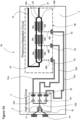
- an electro-optic device 1 comprises an electronic driver 2, an RF medium 3, e.g. a multi-layer interconnect substrate, and a photonic integrated circuit (PIC) 4, which includes a segmented, optical modulator 6, e.g. a Mach-Zehnder optical data modulator (MZM) or a resonant-type optical data modulator.
- the electronic driver 2 includes an input stage 11, which generates an input electrical driver signal, and a plurality of output stages, e.g. three output stages 12a, 12b and 12c, each of which typically generates an approximately identical, about time synchronized, electrical driver signal to be delivered to one of the optical modulation segments of the optical modulator 6.
- Transmission lines 20a, 20b and 20c with varying time delay may be provided on the multi-layer interconnect substrate 3, the photonic integrated circuit (PIC) 4 other some substrate therebetween.
- PIC photonic integrated circuit
- 20a, 20b and 20c provide the overall transmission lines with delays on the multiple copies of the electrical signals, designed to match the corresponding delay on the optical signal traveling through an optical waveguide between segments.
- the delay on the optical signal from the first segment to segment would be t seconds, and the second to the third segment would be another t seconds. This ensures the electrical and optical signals are both synchronized.
- the optical modulator 6 includes an input optical waveguide 21 for receiving an input optical carrier from a light source, e.g. laser, (not shown), and an output optical waveguide 22, for launching a modulated output optical signal.
- the input optical carrier is divided into two sub-beams by an input splitter 23, e.g. a 1x2 optical Y-junction coupler.
- Light of the sub-beams travel along largely parallel first and second optical waveguide arms 24a and 24b to an output combiner 25, e.g. a 1x2 optical Y-junction coupler, which combines the two sub-beams into the modulated output optical signal.
- the modulated output optical signal is output via an optical connector 29, e.g. a surface optical connector on the PIC 4, or an edge optical connector in the PIC 4.
- a plurality of phase-modulating, electro-optical modulator segments are disposed along each of the two optical waveguide arms 24a and 24b, respectively.
- Each of the modulator segments may comprise a differential transmission line, e.g. a first plurality of signal segments 26a along one side of first optical waveguide arm 24a, a first plurality of ground segments 27a along the opposite side of the first optical waveguide arm 24a, a second plurality of signal segments 26b along one side of second optical waveguide arm 24b, and a second plurality of ground segments 27b along the opposite side of the second optical waveguide arm 24b.
- the ground segments and the signal segments may be interchanged.
- the modulator segments are typically radio frequency (RF) traveling wave electrodes for the Mach-Zehnder Interferometers (MZI) or resonant-type optical modulators.
- RF radio frequency
- the RF medium 3 may comprise a substrate built using organic High Density Build Up (HDBU) technology, ceramics or any other high speed, RF compatible, material platform, including back end of the line (BEOL) layers of the silicon photonics process.
- the RF medium 3 may include a plurality of high-speed RF transmission lines, e.g. RF transmission lines 31a, 31b and 31c, one connected to each of the plurality of output stages of the electronic driver 2 RF.
- the RF transmission lines are configured for > 100 Gbps and 3dB bandwidth frequencies in the range of 80-90 GHz, but lower speeds may be possible.
- Each RF transmission line 31a - 31c electrically couples one of the output stages of the electronic driver 2 to the RF transmission lines of a corresponding one of the modulator segments on the PIC 4.
- the lengths of the RF transmission lines 31a, 31b and 31c of the multi-layer interconnect substrate 3 are such that the electrical RF drive signals propagate therethrough to the corresponding modulation segments in approximate synchrony with arrival therein of the same wavefront of the optical signal being modulated.
- propagation of said RF signals through the transmission lines 31a - 31c provide relative delays to synchronize said RF signals with arrival of a portion of the light-to-be-modulated in the various modulation segments of the optical modulator 4.
- the electro-optic device 1 offers the following advantages: 1) The loss from the transmission lines on such platforms are expected to be less than the loss on typical material platforms used for high speed RFICs, such as InP or SiGe. 2) One or more of properties, such as impedance, propagation delay and/or loss of such transmission lines, may be monitored tightly during their fabrication. 3) The combination of highly linear and low loss delay lines on one or combination of both of the multi-layer interconnect substrate 3 and the PIC 4 provides a very compact, high performance solution.
- the RF transmission lines 31a, 31b and 31c may be fabricated in a multi-layer interconnect substrate 3 in which the electrical signals from the electronic driver 2 propagate in the same or different layers that have similar other electromagnetic properties.
- the RF medium 3 may be constructed with metal and with materials having more desirable RF properties, e.g., dielectric having lower RF thermal sensitivity than semiconductor of many optical PICs, whereby a channel pitch of 80-125 ⁇ m may be achieved. For this reason, the interconnect substrate 3 may maintain a more constant relative delay between the RF signals propagating on different RF transmission lines therethrough.
- the RF transmission lines 31a, 31b and 31c are designed on embedded, or internal conductive layers 36 of the substrate 3, with the outermost conductive layers of the substrate 3 being grounded, the properties, and particularly the delays are minimally impacted by packaging and assembly variations; for example, the presence or absence of underfill in a bump bonded region of a device.
- the different signal conductive layers may be separated with 'ground plane levels' ensuring a very high degree of isolation between signals on different conductive layers 36. This approach also ensures high linearity of the signal.
- the RF transmission lines 31a, 31b and 31c of the substrate 3 further delivers the electrical RF drive signals to the PIC 4. Additional RF delay may be applied to one or more of these RF drive signals using linear, low loss delay lines on the PIC 4, as hereinafter described.
- a cross section of an example multi-layer RF interconnect substrate 3 or board includes a plurality of electrical insulator, e.g. dielectric, layers 35 alternating with a plurality of electrical conductor layers 36.
- the electrical insulator layers 35 may be comprised of an organic material, such as is used in conventional High Density Build Up (HDBU) processes, or a ceramic material, such as is formed in High Temperature Co-Fired Ceramic (HTCC) or a Low Temperature Co-Fired Ceramic (LTCC), or an inorganic dielectric material such as silicon dioxide, as in the back end of a silicon or glass or other interposer.
- the electrical conductor layers 36 may be configured, e.g.
- the conductive layers 36 may comprise any suitable electrical conductor(s), e.g. a metal such as copper.
- Vias 37 are filled with one or more electrical conductors, i.e., the same or different electrical conductor as in the electrical conductor layers 36, and may be configured, e.g. etched, vertically through one or more if the electrical insulator layers 35 to contact electrical conductor traces in adjacent electrical conductor layers 36.
- RF medium 3 may be configured, e.g. etched, to include cavities, e.g. cavity 47, for receiving electrical or optical components, e.g. the electronic driver 2 and the PIC 4.
- FIG. 3A and 3B An example of an electro-optic device 41, in which appropriate relative propagation delays between the different RF driving signals are produced by an array of RF transmission lines 31a, 31b and 31c within the multi-layer interconnect substrate 3 of Fig. 1 , is illustrated in Figs. 3A and 3B .
- the high-speed electrical RF drive signals may be transmitted from an external source to electrical contacts 42 on or at an edge of the multi-layer interconnect substrate 3 and subsequently transmitted to the electronic driver 2, via a suitable electrical connection 43, e.g. an array of wire-bonds between electrical connect pads.
- the electrical RF driver signal are transmitted from the parallel array of outputs of the electronic driver 2 to the RF transmission lines 31a, 31b and 31c within a multi-layer interconnect substrate 3 via suitable electrical connection 44, e.g. a parallel array of wire-bonds between electrical connect pads of the outputs and an array of electrical connect pads at ends of the RF transmission lines 31a, 31b, and 31c.
- the electrical RF drive signals are transmitted from the RF delay lines 31a, 31b and 31c within a multi-layer interconnect substrate 3 to the PIC 4 using a suitable electrical connection 46, e.g. wire-bonds between electrical connect pads.
- the electronic driver 2 and the PIC 4 may be mounted at least partially within cavities 47 and 48 formed in the multi-layer interconnect substrate 3.
- the total propagation delay of one of the electrical RF drive signals may be a sum of a propagation delay produced by the corresponding one of the RF delay lines 31a, 31b and 31c within a multi-layer interconnect substrate 3 and a propagation delay produced by an RF transmission line 49a, 49b and 49c in the PIC 4, as disclosed in concurrently filed U.S. Patent Application No. 17/560,809, by Douglas Gill, Juthika Basak, Asres Seyoum, and Matthew Streshinsky , titled "RF DELAY LINE FOR SEGMENTED OPTICAL WAVEGUIDE MODULATOR", which is incorporated herein by reference in its entirety.
- FIG. 4A and 4B A second example 50 of the electro-optic device 1 of Fig. 1 is illustrated in Figs. 4A and 4B .
- elements with already used reference numerals have the same structure and/or function as elements of another figure with the same reference numerals.
- the surface electrical connections 43, 44 and 46 of Figs. 3A-3B e.g. the wire-bond connections, provided on an upper surface of the electronic driver 2, the multi-layer interconnect substrate 3, and the PIC 4 are replaced by more precise flip-chip electrical connections 51, 52 and 53, respectively.
- the flip-chip electrical connections 51, 52 and 53 are between facing surfaces of the electronic driver 2 and the multi-layer interconnect substrate 3 and between facing surfaces of multi-layer interconnect substrate 3 and the PIC 4, e.g., solder bumps and pads provided along the top of the multi-layer interconnect substrate 3.
- the RF transmission lines 49a, 49b and 49c in the PIC 4 may all be the same length, and therefore provide no additional relative propagation delay between the different RF transmission line paths or, alternatively, may provide some additional relative delay.
- the overall propagation delay is a combination of a delay provided by one of the RF transmission lines 31a, 31b and 31c within a multi-layer interconnect substrate 3 as well as the corresponding one of the RF transmission lines 49a, 49b and 49c in the PIC 4.
- total propagation delays can be modified, as desired, using processing or post-processing steps in the semiconductor fabrication flow.
- FIG. 5A and 5B A third example 60 of the electro-optic device 60 of Fig. 1 is illustrated in Figs. 5A and 5B .
- elements with the same reference numerals as other elements of another figure have the same structure and/or function as those other elements.
- Figs. 5A-5B relative propagation delays between RF driver signals are provided by the RF transmission lines 31a, 31b and 31c within a multi-layer interconnect substrate 3.
- the flip-chip bonding connects ends of the RF transmission lines 31a, 31b and 31c to the high speed modulating segments 26a, 26b, 27a and 27b on the multilayer interconnect substrate 3 without causing any additional relative propagation delays, in the PIC 4, between the different RF drive signals.
- FIG. 6A and 6B A fourth example 71 of the electro-optic device 1 of Fig. 1 is illustrated in Figs. 6A and 6B .
- elements with already used reference numerals have the same structure and/or function as elements of another figure with the same reference numerals.
- the electro-optic device 71 may enable a more compact PIC 4, because the relative delays between different electrical RF drive signals are substantially only produced by the RF transmission lines 31a, 31b and 31c within the multi-layer interconnect substrate 3.
- the substrate area under the PIC 4 may be used for RF transmission lines 31a, 31b, 31c, 131a, 131b and 131c with little or no physical overlap. If need be, some small sections of the RF transmission lines 31a, 31b 31c, 131a, 131b and 131c may also be added on the PIC 4 to optimize the total area, looking top-down.
- some or all of the RF transmission lines 31a, 31b and 31c may be formed on different electrical conductor layers 36, but preferably all of the RF transmission lines 31a, 31b and 31c are on a same layer, and all of the RF transmission lines 131a, 131b and 131c are on a same layer, different than RF transmission lines 31a, 31b and 31c.
- the different electrical conductor layers 36 may be separated from each other by ground plane(s) comprising at least a portion of one of the other electrical conductor layers 36 and two of the electrical insulator layers 35 in between the electrical conductor layers 36 including the RF delay lines 31a, 31b and 31c, thereby providing electrical isolation from the other electrical RF drive signals transmitted in the different RF transmission lines 31a, 31b and 31c and the RF transmission lines 131a, 131b and 131c. Accordingly, some or all of RF transmission lines 31a, 31b and 31c may be superposed with RF transmission lines 131a, 131b and 131c, e.g. overlap each other in a top-down view, ( Fig.
- the electronic driver 2 may comprise a plurality of driver structures, e.g. i.e. at least a second electronic driver channel 102, may be provided on the same driver chip. Also, a plurality of optical modulators 6, i.e.
- At least a second optical modulator 106 with similar or different structure than the first optical modulator 6, may be provided on the same PIC 4, e.g., to support in-phase and quadrature phase modulation and/or polarization multiplexing. Also, some of the transmission lines 31a, 31b and 31c from the first optical modulator 6 may laterally overlap the RF transmission lines 131a, 131b and 131c, which produce similar relative propagation delay for electrical RF drive signals to operate the second optical modulator 106. In the multi-layer interconnect substrate 3, the different arrays of transmission lines 31a - 31c and 131a - 131c may be electrically and physically isolated by at least one electrical insulator layer 35 therebetween. A large proportion, e.g.
- RF transmission lines 31a, 31b and 31c from the first modulator 6 and the RF transmission lines 131a, 131b and 131c from second modulator 106 may extend underneath the PIC 4 further reducing the size of the electro-optic device 71.
- RF transmission lines 31a-31c may be on the same layer as each other and different from RF transmission lines 131a-131c, which would be separated in the top-down view as shown on Fig 6A .
- RF transmission lines 131a-131c may be on the same layer as each other but different than RF transmission lines 31a-31c, which ensures that the delay relationship between the RF transmission lines 131a-131c is maintained, since different layers may have slightly different group delay.
- the flip-chip electrical connections 51, 52 and 53 may be between facing surfaces of the electronic driver 2 and the multi-layer interconnect substrate 3 and between facing surfaces of multi-layer interconnect substrate 3 and the PIC 4, e.g. solder bumps and pads provided along the top of the multi-layer interconnect 3 or the bottom on the cavities 47 and 48, if provided.
- All the examples described here provide manufacturing tolerant relative RF propagation delays between RF drive signals operating the different high speed modulating segments 26a, 26b, 27a and 27b of the optical modulators 6, but are often able to maintain a high level of linearity and low RF signal losses.
- the RF transmission lines 31a, 31b and 31c within the multi-layer interconnect substrate 3 can enable high signal integrity in space efficient configurations, making some embodiments suitable for pluggable electro-optic devices, chip on-board or co-packaged high-speed optical transceivers, for applications ranging from optically unamplified links, amplified links, and point-to-point to mesh networks.
Landscapes
- Physics & Mathematics (AREA)
- Nonlinear Science (AREA)
- Optics & Photonics (AREA)
- General Physics & Mathematics (AREA)
- Electromagnetism (AREA)
- Engineering & Computer Science (AREA)
- Computer Networks & Wireless Communication (AREA)
- Signal Processing (AREA)
- Optical Modulation, Optical Deflection, Nonlinear Optics, Optical Demodulation, Optical Logic Elements (AREA)
Applications Claiming Priority (1)
| Application Number | Priority Date | Filing Date | Title |
|---|---|---|---|
| US17/561,071 US20230205043A1 (en) | 2021-12-23 | 2021-12-23 | Multi-segment electro-optic devices with low loss rf delay lines |
Publications (1)
| Publication Number | Publication Date |
|---|---|
| EP4202538A1 true EP4202538A1 (de) | 2023-06-28 |
Family
ID=84535838
Family Applications (1)
| Application Number | Title | Priority Date | Filing Date |
|---|---|---|---|
| EP22213371.2A Pending EP4202538A1 (de) | 2021-12-23 | 2022-12-14 | Mehrteilige elektrooptische vorrichtungen mit verlustarmen hf-verzögerungsleitungen |
Country Status (2)
| Country | Link |
|---|---|
| US (1) | US20230205043A1 (de) |
| EP (1) | EP4202538A1 (de) |
Citations (3)
| Publication number | Priority date | Publication date | Assignee | Title |
|---|---|---|---|---|
| US20160062207A1 (en) * | 2014-08-25 | 2016-03-03 | Futurewei Technologies, Inc. | Multi-Segment Mach-Zehnder Modulator-Driver System |
| US20160363834A1 (en) * | 2013-11-25 | 2016-12-15 | Fraunhofer-Gesellschaft zur Förderung der angewandten Forschung e.V. | Electro-optical modulator devices |
| US20170194310A1 (en) * | 2016-01-04 | 2017-07-06 | Infinera Corporation | Photonic integrated circuit package |
Family Cites Families (3)
| Publication number | Priority date | Publication date | Assignee | Title |
|---|---|---|---|---|
| US8320720B2 (en) * | 2009-08-19 | 2012-11-27 | Mark Webster | Advanced modulation formats for silicon-based optical modulators |
| US10168596B2 (en) * | 2017-05-23 | 2019-01-01 | Elenion Technoogies, LLC | Optical waveguide modulator |
| JP7294066B2 (ja) * | 2019-10-31 | 2023-06-20 | 富士通株式会社 | 光送信機、光トランシーバモジュール、及び光変調方法 |
-
2021
- 2021-12-23 US US17/561,071 patent/US20230205043A1/en active Pending
-
2022
- 2022-12-14 EP EP22213371.2A patent/EP4202538A1/de active Pending
Patent Citations (3)
| Publication number | Priority date | Publication date | Assignee | Title |
|---|---|---|---|---|
| US20160363834A1 (en) * | 2013-11-25 | 2016-12-15 | Fraunhofer-Gesellschaft zur Förderung der angewandten Forschung e.V. | Electro-optical modulator devices |
| US20160062207A1 (en) * | 2014-08-25 | 2016-03-03 | Futurewei Technologies, Inc. | Multi-Segment Mach-Zehnder Modulator-Driver System |
| US20170194310A1 (en) * | 2016-01-04 | 2017-07-06 | Infinera Corporation | Photonic integrated circuit package |
Also Published As
| Publication number | Publication date |
|---|---|
| US20230205043A1 (en) | 2023-06-29 |
Similar Documents
| Publication | Publication Date | Title |
|---|---|---|
| JP7267202B2 (ja) | 変調電極に対して横方向に変位した伝導平面を有する高周波光変調器 | |
| TWI660228B (zh) | IQ light modulator | |
| US6522793B1 (en) | Low voltage electro-optic modulator with integrated driver | |
| CN117997434A (zh) | 集成光收发器、紧凑型光引擎以及多通道光引擎 | |
| US20080118202A1 (en) | Semiconductor chip module | |
| US11940708B2 (en) | Optical modulator | |
| WO2012077337A1 (ja) | 光信号制御装置及び光信号制御方法 | |
| CN110573940B (zh) | 半导体马赫-曾德尔型光调制器 | |
| US8903202B1 (en) | Mach-Zehnder optical modulator having a travelling wave electrode with a distributed ground bridging structure | |
| WO2021084602A1 (ja) | 光モジュール | |
| EP4202538A1 (de) | Mehrteilige elektrooptische vorrichtungen mit verlustarmen hf-verzögerungsleitungen | |
| US10261349B2 (en) | Optical module | |
| JP2016194544A (ja) | 広帯域導波路型光素子 | |
| US11722221B2 (en) | Optical module | |
| WO2021060087A1 (ja) | 光変調器及びそれを用いた光送信装置 | |
| JP2017198908A (ja) | 光送信装置及び光変調器 | |
| WO2021048972A1 (ja) | 半導体マッハツェンダ光変調器およびiq変調器 | |
| JP6638515B2 (ja) | 光変調器 | |
| JP2018077545A (ja) | 光送信装置 |
Legal Events
| Date | Code | Title | Description |
|---|---|---|---|
| PUAI | Public reference made under article 153(3) epc to a published international application that has entered the european phase |
Free format text: ORIGINAL CODE: 0009012 |
|
| STAA | Information on the status of an ep patent application or granted ep patent |
Free format text: STATUS: THE APPLICATION HAS BEEN PUBLISHED |
|
| AK | Designated contracting states |
Kind code of ref document: A1 Designated state(s): AL AT BE BG CH CY CZ DE DK EE ES FI FR GB GR HR HU IE IS IT LI LT LU LV MC ME MK MT NL NO PL PT RO RS SE SI SK SM TR |
|
| STAA | Information on the status of an ep patent application or granted ep patent |
Free format text: STATUS: REQUEST FOR EXAMINATION WAS MADE |
|
| 17P | Request for examination filed |
Effective date: 20231222 |
|
| RBV | Designated contracting states (corrected) |
Designated state(s): AL AT BE BG CH CY CZ DE DK EE ES FI FR GB GR HR HU IE IS IT LI LT LU LV MC ME MK MT NL NO PL PT RO RS SE SI SK SM TR |