EP4202084A2 - Doppellagige elektrolytische kupferfolie und verfahren zu ihrer herstellung - Google Patents
Doppellagige elektrolytische kupferfolie und verfahren zu ihrer herstellung Download PDFInfo
- Publication number
- EP4202084A2 EP4202084A2 EP22193707.1A EP22193707A EP4202084A2 EP 4202084 A2 EP4202084 A2 EP 4202084A2 EP 22193707 A EP22193707 A EP 22193707A EP 4202084 A2 EP4202084 A2 EP 4202084A2
- Authority
- EP
- European Patent Office
- Prior art keywords
- copper foil
- double layered
- electrolyte
- electrolytic copper
- copper layer
- Prior art date
- Legal status (The legal status is an assumption and is not a legal conclusion. Google has not performed a legal analysis and makes no representation as to the accuracy of the status listed.)
- Pending
Links
Images


Classifications
-
- C—CHEMISTRY; METALLURGY
- C25—ELECTROLYTIC OR ELECTROPHORETIC PROCESSES; APPARATUS THEREFOR
- C25D—PROCESSES FOR THE ELECTROLYTIC OR ELECTROPHORETIC PRODUCTION OF COATINGS; ELECTROFORMING; APPARATUS THEREFOR
- C25D1/00—Electroforming
- C25D1/04—Wires; Strips; Foils
-
- B—PERFORMING OPERATIONS; TRANSPORTING
- B32—LAYERED PRODUCTS
- B32B—LAYERED PRODUCTS, i.e. PRODUCTS BUILT-UP OF STRATA OF FLAT OR NON-FLAT, e.g. CELLULAR OR HONEYCOMB, FORM
- B32B15/00—Layered products comprising a layer of metal
- B32B15/04—Layered products comprising a layer of metal comprising metal as the main or only constituent of a layer, which is next to another layer of the same or of a different material
- B32B15/08—Layered products comprising a layer of metal comprising metal as the main or only constituent of a layer, which is next to another layer of the same or of a different material of synthetic resin
-
- B—PERFORMING OPERATIONS; TRANSPORTING
- B32—LAYERED PRODUCTS
- B32B—LAYERED PRODUCTS, i.e. PRODUCTS BUILT-UP OF STRATA OF FLAT OR NON-FLAT, e.g. CELLULAR OR HONEYCOMB, FORM
- B32B15/00—Layered products comprising a layer of metal
- B32B15/20—Layered products comprising a layer of metal comprising aluminium or copper
-
- C—CHEMISTRY; METALLURGY
- C25—ELECTROLYTIC OR ELECTROPHORETIC PROCESSES; APPARATUS THEREFOR
- C25D—PROCESSES FOR THE ELECTROLYTIC OR ELECTROPHORETIC PRODUCTION OF COATINGS; ELECTROFORMING; APPARATUS THEREFOR
- C25D21/00—Processes for servicing or operating cells for electrolytic coating
- C25D21/10—Agitating of electrolytes; Moving of racks
-
- C—CHEMISTRY; METALLURGY
- C25—ELECTROLYTIC OR ELECTROPHORETIC PROCESSES; APPARATUS THEREFOR
- C25D—PROCESSES FOR THE ELECTROLYTIC OR ELECTROPHORETIC PRODUCTION OF COATINGS; ELECTROFORMING; APPARATUS THEREFOR
- C25D21/00—Processes for servicing or operating cells for electrolytic coating
- C25D21/12—Process control or regulation
- C25D21/14—Controlled addition of electrolyte components
-
- C—CHEMISTRY; METALLURGY
- C25—ELECTROLYTIC OR ELECTROPHORETIC PROCESSES; APPARATUS THEREFOR
- C25D—PROCESSES FOR THE ELECTROLYTIC OR ELECTROPHORETIC PRODUCTION OF COATINGS; ELECTROFORMING; APPARATUS THEREFOR
- C25D3/00—Electroplating: Baths therefor
- C25D3/02—Electroplating: Baths therefor from solutions
- C25D3/38—Electroplating: Baths therefor from solutions of copper
-
- C—CHEMISTRY; METALLURGY
- C25—ELECTROLYTIC OR ELECTROPHORETIC PROCESSES; APPARATUS THEREFOR
- C25D—PROCESSES FOR THE ELECTROLYTIC OR ELECTROPHORETIC PRODUCTION OF COATINGS; ELECTROFORMING; APPARATUS THEREFOR
- C25D5/00—Electroplating characterised by the process; Pretreatment or after-treatment of workpieces
- C25D5/10—Electroplating with more than one layer of the same or of different metals
-
- C—CHEMISTRY; METALLURGY
- C25—ELECTROLYTIC OR ELECTROPHORETIC PROCESSES; APPARATUS THEREFOR
- C25D—PROCESSES FOR THE ELECTROLYTIC OR ELECTROPHORETIC PRODUCTION OF COATINGS; ELECTROFORMING; APPARATUS THEREFOR
- C25D5/00—Electroplating characterised by the process; Pretreatment or after-treatment of workpieces
- C25D5/18—Electroplating using modulated, pulsed or reversing current
-
- C—CHEMISTRY; METALLURGY
- C25—ELECTROLYTIC OR ELECTROPHORETIC PROCESSES; APPARATUS THEREFOR
- C25D—PROCESSES FOR THE ELECTROLYTIC OR ELECTROPHORETIC PRODUCTION OF COATINGS; ELECTROFORMING; APPARATUS THEREFOR
- C25D5/00—Electroplating characterised by the process; Pretreatment or after-treatment of workpieces
- C25D5/48—After-treatment of electroplated surfaces
-
- C—CHEMISTRY; METALLURGY
- C25—ELECTROLYTIC OR ELECTROPHORETIC PROCESSES; APPARATUS THEREFOR
- C25D—PROCESSES FOR THE ELECTROLYTIC OR ELECTROPHORETIC PRODUCTION OF COATINGS; ELECTROFORMING; APPARATUS THEREFOR
- C25D5/00—Electroplating characterised by the process; Pretreatment or after-treatment of workpieces
- C25D5/60—Electroplating characterised by the structure or texture of the layers
- C25D5/605—Surface topography of the layers, e.g. rough, dendritic or nodular layers
-
- C—CHEMISTRY; METALLURGY
- C25—ELECTROLYTIC OR ELECTROPHORETIC PROCESSES; APPARATUS THEREFOR
- C25D—PROCESSES FOR THE ELECTROLYTIC OR ELECTROPHORETIC PRODUCTION OF COATINGS; ELECTROFORMING; APPARATUS THEREFOR
- C25D5/00—Electroplating characterised by the process; Pretreatment or after-treatment of workpieces
- C25D5/60—Electroplating characterised by the structure or texture of the layers
- C25D5/615—Microstructure of the layers, e.g. mixed structure
- C25D5/617—Crystalline layers
-
- C—CHEMISTRY; METALLURGY
- C25—ELECTROLYTIC OR ELECTROPHORETIC PROCESSES; APPARATUS THEREFOR
- C25D—PROCESSES FOR THE ELECTROLYTIC OR ELECTROPHORETIC PRODUCTION OF COATINGS; ELECTROFORMING; APPARATUS THEREFOR
- C25D7/00—Electroplating characterised by the article coated
- C25D7/06—Wires; Strips; Foils
- C25D7/0614—Strips or foils
-
- H—ELECTRICITY
- H01—ELECTRIC ELEMENTS
- H01M—PROCESSES OR MEANS, e.g. BATTERIES, FOR THE DIRECT CONVERSION OF CHEMICAL ENERGY INTO ELECTRICAL ENERGY
- H01M4/00—Electrodes
- H01M4/02—Electrodes composed of, or comprising, active material
- H01M4/64—Carriers or collectors
- H01M4/66—Selection of materials
- H01M4/661—Metal or alloys, e.g. alloy coatings
-
- H—ELECTRICITY
- H05—ELECTRIC TECHNIQUES NOT OTHERWISE PROVIDED FOR
- H05K—PRINTED CIRCUITS; CASINGS OR CONSTRUCTIONAL DETAILS OF ELECTRIC APPARATUS; MANUFACTURE OF ASSEMBLAGES OF ELECTRICAL COMPONENTS
- H05K1/00—Printed circuits
- H05K1/02—Details
- H05K1/09—Use of materials for the conductive, e.g. metallic pattern
-
- H—ELECTRICITY
- H05—ELECTRIC TECHNIQUES NOT OTHERWISE PROVIDED FOR
- H05K—PRINTED CIRCUITS; CASINGS OR CONSTRUCTIONAL DETAILS OF ELECTRIC APPARATUS; MANUFACTURE OF ASSEMBLAGES OF ELECTRICAL COMPONENTS
- H05K3/00—Apparatus or processes for manufacturing printed circuits
- H05K3/10—Apparatus or processes for manufacturing printed circuits in which conductive material is applied to the insulating support in such a manner as to form the desired conductive pattern
- H05K3/20—Apparatus or processes for manufacturing printed circuits in which conductive material is applied to the insulating support in such a manner as to form the desired conductive pattern by affixing prefabricated conductor pattern
- H05K3/202—Apparatus or processes for manufacturing printed circuits in which conductive material is applied to the insulating support in such a manner as to form the desired conductive pattern by affixing prefabricated conductor pattern using self-supporting metal foil pattern
-
- C—CHEMISTRY; METALLURGY
- C25—ELECTROLYTIC OR ELECTROPHORETIC PROCESSES; APPARATUS THEREFOR
- C25D—PROCESSES FOR THE ELECTROLYTIC OR ELECTROPHORETIC PRODUCTION OF COATINGS; ELECTROFORMING; APPARATUS THEREFOR
- C25D17/00—Constructional parts, or assemblies thereof, of cells for electrolytic coating
- C25D17/02—Tanks; Installations therefor
-
- H—ELECTRICITY
- H05—ELECTRIC TECHNIQUES NOT OTHERWISE PROVIDED FOR
- H05K—PRINTED CIRCUITS; CASINGS OR CONSTRUCTIONAL DETAILS OF ELECTRIC APPARATUS; MANUFACTURE OF ASSEMBLAGES OF ELECTRICAL COMPONENTS
- H05K2201/00—Indexing scheme relating to printed circuits covered by H05K1/00
- H05K2201/03—Conductive materials
- H05K2201/0332—Structure of the conductor
- H05K2201/0335—Layered conductors or foils
- H05K2201/0355—Metal foils
-
- Y—GENERAL TAGGING OF NEW TECHNOLOGICAL DEVELOPMENTS; GENERAL TAGGING OF CROSS-SECTIONAL TECHNOLOGIES SPANNING OVER SEVERAL SECTIONS OF THE IPC; TECHNICAL SUBJECTS COVERED BY FORMER USPC CROSS-REFERENCE ART COLLECTIONS [XRACs] AND DIGESTS
- Y02—TECHNOLOGIES OR APPLICATIONS FOR MITIGATION OR ADAPTATION AGAINST CLIMATE CHANGE
- Y02E—REDUCTION OF GREENHOUSE GAS [GHG] EMISSIONS, RELATED TO ENERGY GENERATION, TRANSMISSION OR DISTRIBUTION
- Y02E60/00—Enabling technologies; Technologies with a potential or indirect contribution to GHG emissions mitigation
- Y02E60/10—Energy storage using batteries
Definitions
- the present invention relates to a double layered electrolytic copper foil of which various physical properties may be freely controlled to be applicable to various technical fields, and to a method of manufacturing the same.
- an electrolytic copper foil is widely used as a basic material of a printed circuit board (PCB) used in the electric/electronic industry. Accordingly, the demand for such an electrolytic copper foil is rapidly increasing mainly in small products such as slim notebook computers, personal digital assistants (PDA), e-books, MP3 players, next-generation mobile phones, and ultra-thin flat panel displays.
- PDA personal digital assistants
- electrolytic copper foil it is widely used as an anode (e.g., negative electrode) current collector of a secondary battery.
- Such an electrolytic copper foil is prepared in a manner in which sulfuric acid-aqueous solution of copper sulfate is prepared as an electrolyte, a direct current is applied between an anode (e.g., a positive electrode) and a rotating cathode drum (e.g., a negative electrode) immersed in the electrolyte to precipitate an electrodeposited copper on a drum surface, and the precipitated copper electrodeposit is stripped off from the drum surface of the rotating cathode and continuously wound.
- anode e.g., a positive electrode
- a rotating cathode drum e.g., a negative electrode
- the electrolytic copper foil in order to use the electrolytic copper foil as a printed circuit board or a current collector of a secondary battery, it should have various physical properties such as predetermined tensile strength and elongation. However, it is difficult to satisfy the desired physical properties of the copper foil only by the above-described foil-making process. In addition, in order to improve the physical properties of the electrolytic copper foil, it is necessary to perform a separate surface treatment, resulting in complexity of the process and an increase in manufacturing costs.
- aspects of embodiments of the present invention are directed to a double layered electrolytic copper foil of which various physical properties may be freely controlled by controlling process conditions such as electrolyte composition, current density, temperature, and/or agitation when manufacturing the double layered electrolytic copper foil, and a method of manufacturing the same.
- a double layered electrolytic copper foil includes: a first copper layer; a second copper layer; and an interface formed between one surface of the first copper layer and one surface of the second copper layer.
- the first copper layer and the second copper layer may have different grain sizes or different crystal structures from each other.
- the first copper layer, the interface, and the second copper layer may be bonded in a continuous phase through a single electroplating process.
- a double layered structure including the first copper layer, the interface and the second copper layer may be identified by electron backscatter diffraction (EBSD) measured after heat treatment at 200°C for 1 hour and before heat treatment.
- EBSD electron backscatter diffraction
- the interface may be positioned at a thickness in a range from 40 to 60 % of a total thickness of the double layered electrolytic copper foil in a thickness direction of the double layered electrolytic copper foil.
- a thickness ratio of the first copper layer and the second copper layer may be in a range from 40 : 60 to 60 : 40.
- an elongation of the double layered electrolytic copper foil may be in a range from 3.0 to 25 %, and a tensile strength of the double layered electrolytic copper foil may be in a range from 30 to 40 kgf/mm 2 .
- a thickness of the double layered electrolytic copper foil may be in a range from 3 to 70 ⁇ m.
- the double layered electrolytic copper foil may include a drum surface and an electrolyte surface, and a roughness (Rz, ISO) of the electrolyte surface may be in a range from 1.0 to 5.0 ⁇ m.
- a difference in surface roughness between the drum surface and the electrolyte surface may be 1.0 ⁇ m or less.
- the double layered electrolytic copper foil may further include an anti-corrosion layer formed on another surface of the first copper layer and on another surface of the second copper layer.
- the double layered electrolytic copper foil may be applied to at least one of a copper clad laminate, a printed circuit board, and a current collector of a battery.
- the invention concerns a method of manufacturing a double layered electrolytic copper foil by applying a current between an anode and a rotating cathode drum spaced apart from each other in an electrolytic bath in which an electrolyte is accommodated includes: a first step of electrodepositing a first copper layer on the rotating cathode drum by applying a current to the electrolyte; and a second step of electrodepositing a second copper layer on the first copper layer by applying a current to the electrolyte, wherein at least one of a concentration of copper ions included in the electrolyte, a current density, an electrolyte agitation, and an electrolyte temperature is different from each other between the first step and the second step.
- At least one of the concentration of copper ions included in the electrolyte, the electrolyte temperature and the electrolyte agitation circulated on a surface of the cathode drum in the first step may be greater than a corresponding one of the concentration of copper ions included in the electrolyte, the electrolyte temperature and the electrolyte agitation in the second step.
- the current density in the first step may be less than the current density in the second step.
- the electrolyte of the first step and the electrolyte of the second step may be different from each other and may each include copper ions; sulfuric acid; halogen; and at least one additive of a brightener, a leveler, a suppressor and a carrier.
- the method may further include: performing at least one of a nodule treatment and an anti-corrosion treatment on the electrodeposited double layered electrolytic copper foil.
- a double layered electrolytic copper foil of which various physical properties may be freely controlled by controlling process conditions such as electrolyte composition, current density, temperature, and/or agitation when manufacturing the electrolytic copper foil, and a method of manufacturing the same may be provided.
- preferred and preferably refer to embodiments of the present invention that may provide certain advantages under certain circumstances. However, other embodiments may also be preferred, under the same or other circumstances. Additionally, the recitation of one or more preferred embodiments does not imply that other embodiments are not useful, nor is it intended to exclude other embodiments from the scope of the invention.
- An example of the present invention is an electrolytic copper foil applicable to a current collector of a secondary battery, a copper clad laminate (CCL), and/or a printed circuit board (PCB).
- Such an electrolytic copper foil is differentiated from the conventional copper foil in that the electrolytic copper foil according to the present invention includes a copper foil of double layers having different grain sizes, different crystal structures, or different physical properties from each other without a separate compression or bonding process.
- the electrolytic copper foil is generally formed of a single layer through a foil making process, there is a problem in that it is difficult to control various physical properties such as tensile strength and elongation as desired.
- a separate surface treatment process may be performed or a functional layer for supplementing the physical properties of the copper foil may be additionally bonded, but in such a case, complexity of the process and increase in manufacturing costs are inevitably caused.
- a double layered structure is formed by controlling process conditions such as electrolyte composition, current density, temperature, and/or agitation (e.g., flow rate) differently when manufacturing a first copper layer and a second copper layer forming the double layered structure.
- process conditions such as electrolyte composition, current density, temperature, and/or agitation (e.g., flow rate) differently when manufacturing a first copper layer and a second copper layer forming the double layered structure.
- respective copper plating layers constituting the double layered structure may be implemented to have different physical properties from each other by controlling the above-described process conditions, various physical properties of the final double layered electrolytic copper foil may be freely controlled by controlling the physical properties and thickness of these copper plating layers.
- first copper layer and the second copper layer are connected with a continuous interface through a single electroplating process, physical stability is remarkably improved as compared to the conventional art of constructing a double layered copper foil by separate compression or bonding.
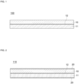
- FIG. 1 is a cross-sectional view illustrating a structure of an electrolytic copper foil according to an embodiment of the present invention.
- a double layered electrolytic copper foil 100 includes a first copper layer 11; a second copper layer 12; and an interface 13 continuously formed between the first copper layer 11 and the second copper layer 12.
- the first copper layer 11 and the second copper layer 12 may be different from each other in terms of a grain size constituting the copper foil, a crystal structure, and/or at least one of various physical properties required as a copper foil.
- various physical properties may include, but are not particularly limited to, tensile strength and elongation.
- the double layered electrolytic copper foil 100 is an electrolytic copper foil doubly electrodeposited by a continuous electrolysis method. Accordingly, the first copper layer 11, the interface 13, and the second copper layer 12 constituting the double layered structure are bonded in a continuous phase through a single electroplating process, and the interface is present at a predetermined position along a thickness direction of the double layered electrolytic copper foil 100.
- the above-described double layered structure including the first copper layer 11, the interface 13, and the second copper layer 12 may be confirmed by a scanning electron microscope (SEM) photograph illustrating a cross-section of the double layered electrolytic copper foil 100, and specifically, it may be confirmed by electron backscatter diffraction (EBSD) of the electrolytic copper foil measured after heat treatment at 200°C for 1 hour and before heat treatment.
- SEM scanning electron microscope
- EBSD electron backscatter diffraction
- the interface 13 may be positioned at (e.g., within) a thickness in a range from 40 % to 60 % of a total thickness of the double layered electrolytic copper foil 100 in a thickness direction of the double layered electrolytic copper foil 100.
- the position of the interface 13 may be based on one surface of the double layered electrolytic copper foil 100, that is, an electrolyte surface (M surface).
- a shiny surface e.g., "S surface”, drum surface, etc.
- a matte surface e.g., an "M surface”, an electrolyte surface, etc. which has a relatively high roughness due to so-called mountain structures and thus has a low gloss is formed on another surface thereof.
- a bonding force with an active material and a yield of the battery may greatly vary depending on a surface state of the double layered electrolytic copper foil 100.
- surface non-uniformity due to the surface roughness of the copper foil is too high, there is a problem in that a discharge-capacity retention rate of the secondary battery is lowered, and on the other hand, when the surface of the copper foil is too uniform, it may be difficult to secure the binding force between the current collector and the active material, and thus the active material may be desorbed from the current collector during operation of the secondary battery, thereby causing problems such as an internal short circuit.
- a difference in a coating amount of the active material between the opposite surfaces may be caused.
- the non-uniform coating amount between the opposite surfaces may cause a problem that a capacity of the electrode may decrease and/or unstable behavior of the electrode may occur due to a difference in deformation between the opposite surfaces of the current collector.
- by adjusting the surface roughness of the double layered electrolytic copper foil 100 to a predetermined range it is possible to secure required physical properties of the double layered electrolytic copper foil 100, that is, an excellent bonding FORCE with the active materials and a high discharge capacity retention rate.
- the double layered electrolytic copper foil 100 includes a drum surface and an electrolyte surface, and a surface roughness of the electrolyte surface may be in a range from approximately 1.0 to 5.0 ⁇ m, and specifically in a range from 1.0 to 4.0 ⁇ m, in terms of Rz (ten-point average roughness). More specifically, the surface roughness of the drum surface (e.g., S surface) of the copper foil may be in a range from 1.0 to 2.0 ⁇ m, and the surface roughness of the electrolyte surface (e.g., M surface) may be in a range from 1.0 to 5.0 ⁇ m.
- the surface roughness of the drum surface (e.g., S surface) of the copper foil may be in a range from 1.0 to 2.0 ⁇ m
- the surface roughness of the electrolyte surface e.g., M surface
- a difference in surface roughness between the drum surface and the electrolyte surface of the double layered electrolytic copper foil 100 may be 1.0 ⁇ m or less, and specifically, 0.5 ⁇ m or less.
- a thickness of the double layered electrolytic copper foil 100 may have a typical thickness range known in the art, but the present invention is not particularly limited thereto.
- the thickness of the double layered electrolytic copper foil 100 may be in a range from 3 ⁇ m to 70 ⁇ m, specifically, in a range from 4 to 70 ⁇ m, and more specifically in a range from 15 to 70 ⁇ m.
- the thickness of the double layered electrolytic copper foil 100 is too thin, it is difficult to handle the copper foil in a manufacturing process, thus lowering the workability, and on the other hand, when the thickness of the double layered electrolytic copper foil 100 is too thick, volume and weight may increase due to its thickness when the double layered electrolytic copper foil 100 is used as a current collector.
- a thickness ratio of the first copper layer 11 and the second copper layer 12 constituting the double layered structure may be in a range from 40 to 60 : 60 to 40, but the present invention is not particularly limited thereto, and it may be appropriately adjusted considering various physical properties of the final double layered electrolytic copper foil.
- the double layered electrolytic copper foil 100 according to the present invention preferably has excellent elongation and tensile strength, considering mechanical hardness, flexibility, and product reliability.
- the double layered electrolytic copper foil 100 may have an elongation in a range from 3.0 to 25 % and a tensile strength in a range from 30 to 40 kgf/mm 2 , and more specifically, an elongation in a range from 3.2 to 23.0 % and a tensile strength in a range from 30 to 39.8 kgf/mm 2 .
- the present invention is not limited thereto, and the elongation and the tensile strength may be appropriately adjusted considering the physical properties of the final double layered electrolytic copper foil.
- the above-described physical properties of the double layered electrolytic copper foil 100 according to the present invention may be based on a thickness in a range from 3 to 200 ⁇ m of the copper foil.
- the present invention is not limited to the above-described thickness range.
- the double layered electrolytic copper foil 100 according to the present invention is not particularly limited in terms of, for example, components, composition, and/or structure constituting the copper foil, as long as it has a double layered structure through a single electrolytic plating process without separate compression or bonding.
- Each of the first copper layer 11 and the second copper layer 12 may include or be formed of copper or copper alloy known in the art, and in such a case, the metal component included in the alloy is not particularly limited, and a conventional metal known in the art may be used.
- Each of the first copper layer 11 and the second copper layer 12 is a copper plating layer formed through electroplating in which a current is applied between an anode (e.g., positive electrode) plate and a rotating cathode (e.g., negative electrode) drum which are spaced apart from each other in an electrolyte.
- Each of the first copper layer 11 and the second copper layer 12 may be a general copper foil, a double-sided glossy copper foil, a high elongation copper foil, and/or a high strength (e.g., high tensile strength) copper foil according to electrolyte composition including copper ions and at least one additive, the type of additive applied, and/or their content control, but the present invention is not particularly limited thereto.
- the double layered electrolytic copper foil 100 may be in a foil shape, specifically, may be a flat copper foil.
- the double layered electrolytic copper foil 100 may include an anti-corrosion layer (e.g., rust prevention layer) 20 formed on a surface thereof.
- the anti-corrosion layer 20 may be formed on a surface (e.g., another surface) opposite to one surface of the first copper layer 11 contacting the interface 13 and on a surface (e.g., another surface) opposite to one surface of the second copper layer 12 contacting the interface 13.
- the anti-corrosion layer 20 is selectively formed on an outermost surface of the double layered electrolytic copper foil 100 to prevent corrosion (e.g., rust).
- the anti-corrosion layer 20 may include conventional inorganic corrosion-resistant (e.g., rust-preventive) materials, organic corrosion-resistant materials, or mixtures thereof known in the art, for example, at least one or more of chromium (Cr), molybdenum (Mo), nickel (Ni), a silane compound, and a nitrogen compound.
- the nitrogen compound may include at least one or more of common triazole compounds and amine compounds known in the art.
- the applicable triazole compound may be selected from, for example, benzotriazole, tolyltriazole, carboxybenzotriazole, chlorobenzotriazole, ethylbenzotriazole and naphthotriazole.
- available amine compounds may be selected from, for example, amide, acrylamide, acetamide, auramine, dodecyltrimethyl ammonium bromide (DTAB) and diethylenetriamine (DETA).
- the anti-corrosion layer 20 may serve to impart not only the anti-corrosion properties to the double layered electrolytic copper foil 100 described above, but also heat-resistance properties and/or properties to increase a bonding force with active materials.
- the present invention is not limited only by the following manufacturing method or sequence, and steps of each process may be modified or selectively mixed as needed.
- the double layered electrolytic copper foil 100 according to the present invention may be manufactured through a conventional electrolytic foiling apparatus in the art.
- a drum 220 serving as a cathode and an anode plate 210 are installed in an electrolytic bath 240 to which an electrolyte 250 is continuously supplied, and a predetermined current is applied in a state that the drum 220 and the anode plate 210 are spaced apart from each other so that the electrolyte 250 may be interposed therebetween.
- an electrolytic copper foil 260 is electrodeposited on a surface of the drum 220, and then the electrodeposited electrolytic copper foil 260 is wound through a guide roll 270.
- an electrolytic bath including a plurality of inlets 231 and 232 for supplying electrolytes having different compositions, and an electrolyte input controller 230 including a valve 233 for opening and closing the inlets 231 and 232 may be used.
- Such an electrolytic bath is not particularly limited, but may include, for example, a first inlet for supplying a first electrolyte, a second inlet for supplying a second electrolyte, and a valve for opening and closing the first inlet and the second inlet.
- the method of manufacturing the double layered electrolytic copper foil may include a first step of electrodepositing a first copper layer on the rotating cathode drum by applying a current to a first electrolyte provided in an electrolytic bath; and a second step of electrodepositing a second copper layer on the first copper layer by applying a current to a second electrolyte, where the process conditions of each step may be adjusted within a predetermined range.
- the anode 210 in a semi-cylindrical shape and the rotating cathode drum 220 are disposed apart from each other at a predetermined interval in the electrolytic bath 240 including the first inlet 231, the second inlet 232, and the valve 233.
- the anode 210 is not particularly limited, and for example, a lead alloy or titanium coated with iridium oxide may be used.
- a lead alloy or titanium coated with iridium oxide may be used as the cathode 220.
- chromium-plated stainless steel may be used as the cathode 220.
- the present invention is not limited thereto.
- the first electrolyte is continuously supplied between the anode 210 and the rotating cathode drum 220 in the electrolytic bath 240 through the first inlet 231 provided in the electrolytic bath 240. Then, when a direct current is applied between the anode 210 and the cathode 220, in the cathode 220, copper ions in the first electrolyte are reduced to a metal of a predetermined thickness and precipitated, thereby forming the first copper layer.
- At least one of the process conditions of the first step of electrodepositing the first copper layer and the process conditions of the second step of electrodepositing the second copper layer for example, at least one process condition of a concentration of copper ions included in the electrolyte, an applied current density, a temperature of the electrolyte, and an agitation (e.g., flow rate) of the electrolyte supplied to or circulated on the cathode drum is controlled differently.
- the grain size or crystal structure of the electrodeposited copper layer may be controlled.
- process conditions such as copper ion concentration, current density, agitation, and electrolyte temperature during electroplating
- the grain size or crystal structure of the electrodeposited copper layer may be controlled.
- the grain size is large, a tensile strength of the copper foil decreases and an elongation increases, and on the other hand, when the grain size is small, the tensile strength of the copper foil increases and the elongation decreases.
- the concentration of copper ions in the electrolyte is increased, the grain size increases due to a decrease in surface polarization, and the tensile strength decreases, but the elongation increases.
- the speed, that is, agitation, of the electrolyte supplied to or circulated on the drum surface increases, copper ions are smoothly supplied to the drum surface, resulting in increased copper ion concentration in the electrolyte, such that grains become large, the tensile strength decreases, and the elongation increases.
- additives included in the electrolyte may increase or decrease the grain size according to the unique properties of the additives. For example, a brightener accelerates self-annealing to increase the grain size, and conversely, a leveler decreases the grain size.
- the first electrolyte for forming the first copper layer 11 and the second electrolyte for forming the second copper layer 12 may each use conventional electroplating electrolyte components known in the art without limitation.
- the first electrolyte and the second electrolyte may be different from each other and may each include copper ions; sulfuric acid; halogen; and at least one additive of a brightener, a leveler, a suppressor (e.g., inhibitor) and a carrier.
- each of the first electrolyte and the second electrolyte may include copper ions in an amount ranging from 50 to 120 g/L, and specifically, 60 to 100 g/L, and may include copper sulfate including, for example, 50 to 150 g/L of sulfuric acid.
- a chlorine ion concentration may be in a range from 0.1 to 70 ppm, and a concentration of organic impurities (TOC) in the electrolyte may be limited to 1000 ppm.
- any additive commonly used in the field of electroplating may be used without limitation.
- a sulphonate-based additive including sulfide as an accelerator (brightener) for imparting gloss to the plating surface and obtaining a fine plating layer a gelatin having a molecular weight in a range from 1,000 to 100,000, polyethylene glycols (PEG), polypropylene glycols (PPG), or a low molecular weight gelatin as a carrier for controlling a roughness of the copper foil; a cellulose-based additive as a suppressor for realizing stable low roughness; and/or a mixture of one or more kind thereof may be included.
- Applicable organic additives may include hydroxyethyl cellulose (HEC), 3-(benzothiazolyl-2-mercapto)-propyl-sulfonic acid, low molecular weight nitrides (e.g., thiourea series, amides, benzimidazole series, benthiazol series, dimethyl aniline, etc.) as a leveler for lowering roughness of the copper foil and imparting high strength (e.g., tensile strength).
- HEC hydroxyethyl cellulose
- 3-(benzothiazolyl-2-mercapto)-propyl-sulfonic acid low molecular weight nitrides (e.g., thiourea series, amides, benzimidazole series, benthiazol series, dimethyl aniline, etc.) as a leveler for lowering roughness of the copper foil and imparting high strength (e.g., tensile strength).
- a specific example of the above-described at least one additive may include 1 to 3000 ppm of HEC, bis-(3-sulfopropyl) disulfide (SPS) as the brightener/accelerator, 0.5 to 1500 ppm of 3-mercaptopropyl sulfonate (MPS), 1 to 10000 ppm of a low molecular weight gelatin, and 0.05 to 1500 ppm of thiourea.
- SPS bis-(3-sulfopropyl) disulfide
- MPS 3-mercaptopropyl sulfonate
- the present invention is not particularly limited thereto.
- the electroplating conditions for each step are not particularly limited, and may be appropriately adjusted within a range known in the art.
- the current densities applied to the first electrolyte and/or the second electrolyte may be the same as or different from each other, specifically in a range from 30 to 100 A/dm 2 , and more specifically in a range from 40 to 80 A/dm 2 .
- temperatures of the first electrolyte and/or the second electrolyte may be the same as or different from each other, for example, in a range from 35 to 75°C, and specifically in a range from 40 to 60°C.
- the agitations of the first electrolyte and the second electrolyte may be the same as or different from each other, for example, in a range from 30 to 120 m 3 /hr, and specifically in a range from 50 to 100 m 3 /hr.
- the present invention is not particularly limited to the above-described range.
- the double layered electrolytic copper foil 100 may be obtained
- the obtained double layered electrolytic copper foil 100 may be further subjected to at least one surface treatment of nodule treatment and rust prevention treatment known in the art.
- the double layered electrolytic copper foil 100 including the first copper layer 11 and the second copper layer 12 has been specifically illustrated and described.
- the present invention is not limited thereto, and it is also within the scope of the present invention to constitute an electrolytic copper foil having a multilayer structure of three or more layers.
- the double layered electrolytic copper foil 100 of the present invention manufactured as described above, various physical properties required as a copper foil, for example, tensile strength, elongation, hardness, and/or flexibility may be freely controlled, while effectively controlling factors such as a difference in roughness between opposite surfaces and a thickness ratio between each copper layer. Accordingly, the double layered electrolytic copper foil 100 may be usefully used as a copper clad laminate, a printed circuit board, and/or a current collector of a battery. In addition, it may be applicable without limitation to various technical fields in which copper foil is used in the pertinent art.
- a double layered electrolytic copper foil was manufactured using the electrolytic apparatus illustrated in FIG. 3 .
- a first copper layer was formed by adding a first electrolyte into an electrolytic bath, immersing an anode and a rotating cathode drum to be spaced apart from each other in a first electrolyte, and applying a current therebetween. Specifically, in order to prepare the first electrolyte, adjustment was made to a copper ion concentration of 70 g/L or 80 g/L, a sulfuric acid concentration of 100 g/L, and a chloride ion concentration of 35 ppm at a temperature of 60°C.
- an additive G included a low molecular weight gelatin (molecular weight of 3,000), an additive B included 3-mercaptopropyl sulfonate (MPS), and an additive T included thiourea as a leveler, and their contents were G (3.5 ppm), B (1.5 ppm), T (0.2 ppm), respectively.
- G 3.5 ppm
- B 1.5 ppm
- T 0.2 ppm
- the composition of the first electrolyte, current density, temperature, and agitation conditions for forming the first copper layer are respectively as shown in A of Table 1 below.
- a second copper layer was electrodeposited on the first copper layer by controlling the current density, temperature, and agitation conditions.
- the composition of the second electrolyte, current density, temperature, and agitation conditions for forming the second copper layer are as shown in B or C of Table 1 below.
- chromium (Cr) treatment was performed through immersion in a small bath to give corrosion preventing ability.
- Electrolytic copper foils of Comparative Examples 1 to 4 were manufactured in the same manner as in Example 1, except that the electrolysis conditions were changed as shown in Table 1 above.
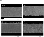
- FIG. 4 is a SEM photograph illustrating a cross-section of a double layered electrolytic copper foil prepared in Examples 1 to 4
- FIG. 5 is an SEM photograph illustrating a cross-section of a single-layer electrolytic copper foil prepared in Comparative Example 1.
- the electrolytic copper foils of Examples 1 to 4 have a double layered structure including a first copper layer and a second copper layer, and that a continuous interface was formed between the first copper layer and the second copper layer (see FIG. 4 ).
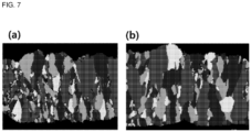
- EBSD electron backscatter diffraction
- Example 1 the electrolytic copper foils prepared in Example 1 and Comparative Example 1 were used. EBSD analysis was performed using the electrolytic copper foil before heat treatment, and then, after heat treatment at 200°C for 1 hour, EBSD analysis was performed again.
- Bruker's equipment was used for EBSD analysis, and a minimum pixel size was set to 100 nm or less, and a magnification was set to 5000 times. Analysis was conducted based on results of orientation and diffraction patterns of materials analyzed using a pattern quality map (PQ map) and an inverse pole figure map (IPF map).
- PQ map expresses a difference in signal intensity of electric charges (e.g., electrons, backscattered electrons) reflected from the sample as a difference in contrast (e.g., light and dark), and is generally expressed darkly at grain boundaries because the signal is weak.
- the IPF Map expresses a difference in a crystal direction (orientation) of the sample in color.
- the term "twin" means a plane that is 60° misorientated with respect to a crystal plane of the sample.
- FIG. 6 is an EBSD image of the double layered electrolytic copper foil prepared in Example 1 before heat treatment ( FIG. 6A ) and after heat treatment ( FIG. 6B )
- FIG. 7 is an EBSD image of the electrolytic copper foil prepared in Comparative Example 1 before heat treatment ( FIG. 7A ) and after heat treatment ( FIG. 7B ).
- twin boundaries are removed.
- a thickness was measured by a unit basis weight method, which is a typical thickness measurement method of copper foil (IPC-TM-650 2.2.12).
- a roughness of the copper foil was measured based on Rz using a shape measuring instrument (MarSurf, model name: M 300 C Mobile roughness measuring instrument) (IPC-TM-650 2.2.17).
- various physical properties required as a copper foil for example, tensile strength, elongation, and roughness, may be freely controlled by controlling at least one electrolysis conditions such as electrolyte composition, current density, temperature, and/or agitation.
- the double layered electrolytic copper foil according to the present invention may be usefully applied to various fields in which copper foil is used in the pertinent art, for example, a copper clad laminate, a printed circuit board, and/or a current collector of a battery.
Landscapes
- Chemical & Material Sciences (AREA)
- Engineering & Computer Science (AREA)
- Chemical Kinetics & Catalysis (AREA)
- Electrochemistry (AREA)
- Materials Engineering (AREA)
- Metallurgy (AREA)
- Organic Chemistry (AREA)
- Microelectronics & Electronic Packaging (AREA)
- Crystallography & Structural Chemistry (AREA)
- General Chemical & Material Sciences (AREA)
- Automation & Control Theory (AREA)
- Manufacturing & Machinery (AREA)
- Cell Electrode Carriers And Collectors (AREA)
- Electrolytic Production Of Metals (AREA)
- Laminated Bodies (AREA)
- Electroplating And Plating Baths Therefor (AREA)
- Electroplating Methods And Accessories (AREA)
Applications Claiming Priority (1)
| Application Number | Priority Date | Filing Date | Title |
|---|---|---|---|
| PCT/EP2021/087638 WO2023117126A1 (en) | 2021-12-24 | 2021-12-24 | Double layered electrolytic copper foil and manufacturing method thereof |
Publications (2)
| Publication Number | Publication Date |
|---|---|
| EP4202084A2 true EP4202084A2 (de) | 2023-06-28 |
| EP4202084A3 EP4202084A3 (de) | 2023-10-04 |
Family
ID=80113443
Family Applications (1)
| Application Number | Title | Priority Date | Filing Date |
|---|---|---|---|
| EP22193707.1A Pending EP4202084A3 (de) | 2021-12-24 | 2022-09-02 | Doppellagige elektrolytische kupferfolie und verfahren zu ihrer herstellung |
Country Status (4)
| Country | Link |
|---|---|
| US (1) | US20230203691A1 (de) |
| EP (1) | EP4202084A3 (de) |
| KR (1) | KR102681509B1 (de) |
| WO (1) | WO2023117126A1 (de) |
Families Citing this family (1)
| Publication number | Priority date | Publication date | Assignee | Title |
|---|---|---|---|---|
| KR20260038452A (ko) * | 2024-09-12 | 2026-03-19 | 삼성에스디아이 주식회사 | 리튬 이차 전지용 복합 기재, 이의 제조 방법 및 이를 포함하는 리튬 이차 전지 |
Family Cites Families (8)
| Publication number | Priority date | Publication date | Assignee | Title |
|---|---|---|---|---|
| US5215646A (en) * | 1992-05-06 | 1993-06-01 | Circuit Foil Usa, Inc. | Low profile copper foil and process and apparatus for making bondable metal foils |
| CN101146933B (zh) * | 2005-03-31 | 2010-11-24 | 三井金属矿业株式会社 | 电解铜箔及电解铜箔的制造方法、采用该电解铜箔得到的表面处理电解铜箔、采用该表面处理电解铜箔的覆铜层压板及印刷电路板 |
| TW200847867A (en) * | 2007-04-26 | 2008-12-01 | Mitsui Mining & Smelting Co | Printed wire board and manufacturing method thereof, and electrolytic copper foil for copper-clad lamination board used for manufacturing the same |
| KR101133195B1 (ko) * | 2009-08-31 | 2012-04-09 | 엘에스엠트론 주식회사 | 리튬 이차전지 집전체용 동박 |
| WO2013129588A1 (ja) * | 2012-02-28 | 2013-09-06 | 古河電気工業株式会社 | リチウムイオン二次電池、該二次電池の負極電極を構成する集電体、ならびに該負極電極集電体を構成する電解銅箔 |
| KR20170085425A (ko) * | 2016-01-13 | 2017-07-24 | 엘에스엠트론 주식회사 | 동박, 그 제조방법, 그것을 포함하는 전극, 및 그것을 포함하는 이차전지 |
| WO2017123034A1 (ko) * | 2016-01-13 | 2017-07-20 | 엘에스엠트론 주식회사 | 동박, 그 제조방법, 그것을 포함하는 전극, 및 그것을 포함하는 이차전지 |
| KR102413056B1 (ko) * | 2017-07-18 | 2022-06-23 | 에스케이넥실리스 주식회사 | 주름이 방지되고 우수한 충방전 특성을 갖는 동박, 그것을 포함하는 전극, 그것을 포함하는 이차전지, 및 그것의 제조방법 |
-
2021
- 2021-12-24 WO PCT/EP2021/087638 patent/WO2023117126A1/en not_active Ceased
-
2022
- 2022-09-02 EP EP22193707.1A patent/EP4202084A3/de active Pending
- 2022-09-21 KR KR1020220119393A patent/KR102681509B1/ko active Active
- 2022-11-16 US US17/988,405 patent/US20230203691A1/en active Pending
Also Published As
| Publication number | Publication date |
|---|---|
| WO2023117126A1 (en) | 2023-06-29 |
| US20230203691A1 (en) | 2023-06-29 |
| EP4202084A3 (de) | 2023-10-04 |
| KR20230097988A (ko) | 2023-07-03 |
| CA3172490A1 (en) | 2023-06-24 |
| KR102681509B1 (ko) | 2024-07-03 |
Similar Documents
| Publication | Publication Date | Title |
|---|---|---|
| US9307639B2 (en) | Electro-deposited copper foil, surface-treated copper foil using the electro-deposited copper foil and copper clad laminate using the surface-treated copper foil, and a method for manufacturing the electro-deposited copper foil | |
| KR100389061B1 (ko) | 전해 동박 제조용 전해액 및 이를 이용한 전해 동박 제조방법 | |
| JP3058445B2 (ja) | 特性の調整された、印刷回路基板用の電着された箔並びにそれを製造するための方法及び電解槽溶液 | |
| JP5255229B2 (ja) | 電解銅箔、その電解銅箔を用いた表面処理銅箔及びその表面処理銅箔を用いた銅張積層板並びにその電解銅箔の製造方法 | |
| CN112543822B (zh) | 电解铜箔的制造方法 | |
| CN110093637A (zh) | 用于挠性覆铜板、挠性印制电路板的电解铜箔及制备方法 | |
| US5171417A (en) | Copper foils for printed circuit board applications and procedures and electrolyte bath solutions for electrodepositing the same | |
| US11118279B2 (en) | Electrolytic copper foil for secondary battery and method for producing the same | |
| JP2022050471A (ja) | 耐屈曲性に優れた二次電池用電解銅箔及びその製造方法 | |
| US20240097139A1 (en) | Electrolytic copper foil and secondary battery comprising the same | |
| EP4202084A2 (de) | Doppellagige elektrolytische kupferfolie und verfahren zu ihrer herstellung | |
| EP3540835A1 (de) | Elektrolytische kupferfolie für eine sekundärbatterie und verfahren zur herstellung davon | |
| EP3067442A1 (de) | Elektrolytische kupferfolie, elektrische komponente und batterie damit | |
| KR102323903B1 (ko) | 연성인쇄회로기판의 치수안정성을 향상시킬 수 있는 동박, 그 제조방법, 및 그것을 포함하는 연성동박적층필름 | |
| CA3172490C (en) | Double layered electrolytic copper foil and manufacturing method thereof | |
| KR102934028B1 (ko) | 전해 동박 및 이를 포함하는 이차전지 | |
| US12431507B2 (en) | Electrolytic copper foil and secondary battery comprising the same | |
| CA3172018C (en) | Electrolytic copper foil and secondary battery comprising the same | |
| US20230207830A1 (en) | Electrolytic copper foil having high tensile strength and secondary battery comprising the same | |
| EP4641708A1 (de) | Metallfolie mit hervorragender bruchdehnung und sekundärbatterie damit | |
| JP2005008973A (ja) | 銅箔の表面粗化方法 | |
| JP2008081836A (ja) | 強度、導電率、曲げ加工性に優れた銅合金条又は銅合金箔の製造方法、銅合金条又は銅合金箔、並びにそれを用いた電子部品 |
Legal Events
| Date | Code | Title | Description |
|---|---|---|---|
| PUAI | Public reference made under article 153(3) epc to a published international application that has entered the european phase |
Free format text: ORIGINAL CODE: 0009012 |
|
| STAA | Information on the status of an ep patent application or granted ep patent |
Free format text: STATUS: REQUEST FOR EXAMINATION WAS MADE |
|
| 17P | Request for examination filed |
Effective date: 20220902 |
|
| AK | Designated contracting states |
Kind code of ref document: A2 Designated state(s): AL AT BE BG CH CY CZ DE DK EE ES FI FR GB GR HR HU IE IS IT LI LT LU LV MC MK MT NL NO PL PT RO RS SE SI SK SM TR |
|
| RIC1 | Information provided on ipc code assigned before grant |
Ipc: C25D 17/02 20060101ALI20230712BHEP Ipc: C25D 21/14 20060101ALI20230712BHEP Ipc: C25D 21/10 20060101ALI20230712BHEP Ipc: C25D 5/18 20060101ALI20230712BHEP Ipc: C25D 5/10 20060101ALI20230712BHEP Ipc: C25D 3/38 20060101ALI20230712BHEP Ipc: C25D 1/04 20060101AFI20230712BHEP |
|
| PUAL | Search report despatched |
Free format text: ORIGINAL CODE: 0009013 |
|
| STAA | Information on the status of an ep patent application or granted ep patent |
Free format text: STATUS: EXAMINATION IS IN PROGRESS |
|
| AK | Designated contracting states |
Kind code of ref document: A3 Designated state(s): AL AT BE BG CH CY CZ DE DK EE ES FI FR GB GR HR HU IE IS IT LI LT LU LV MC MK MT NL NO PL PT RO RS SE SI SK SM TR |
|
| RIC1 | Information provided on ipc code assigned before grant |
Ipc: C25D 17/02 20060101ALI20230828BHEP Ipc: C25D 21/14 20060101ALI20230828BHEP Ipc: C25D 21/10 20060101ALI20230828BHEP Ipc: C25D 5/18 20060101ALI20230828BHEP Ipc: C25D 5/10 20060101ALI20230828BHEP Ipc: C25D 3/38 20060101ALI20230828BHEP Ipc: C25D 1/04 20060101AFI20230828BHEP |
|
| 17Q | First examination report despatched |
Effective date: 20230913 |
|
| RAP1 | Party data changed (applicant data changed or rights of an application transferred) |
Owner name: VOLTA ENERGY SOLUTIONS S.A R.L. |