EP4199086A1 - Capacitor array structure, manufacturing method therefor, and semiconductor storage device - Google Patents
Capacitor array structure, manufacturing method therefor, and semiconductor storage device Download PDFInfo
- Publication number
- EP4199086A1 EP4199086A1 EP21870924.4A EP21870924A EP4199086A1 EP 4199086 A1 EP4199086 A1 EP 4199086A1 EP 21870924 A EP21870924 A EP 21870924A EP 4199086 A1 EP4199086 A1 EP 4199086A1
- Authority
- EP
- European Patent Office
- Prior art keywords
- layer
- capacitor
- array structure
- gas
- top electrode
- Prior art date
- Legal status (The legal status is an assumption and is not a legal conclusion. Google has not performed a legal analysis and makes no representation as to the accuracy of the status listed.)
- Pending
Links
Images



Classifications
-
- H—ELECTRICITY
- H10—SEMICONDUCTOR DEVICES; ELECTRIC SOLID-STATE DEVICES NOT OTHERWISE PROVIDED FOR
- H10D—INORGANIC ELECTRIC SEMICONDUCTOR DEVICES
- H10D1/00—Resistors, capacitors or inductors
- H10D1/60—Capacitors
- H10D1/68—Capacitors having no potential barriers
- H10D1/692—Electrodes
- H10D1/696—Electrodes comprising multiple layers, e.g. comprising a barrier layer and a metal layer
-
- H—ELECTRICITY
- H10—SEMICONDUCTOR DEVICES; ELECTRIC SOLID-STATE DEVICES NOT OTHERWISE PROVIDED FOR
- H10B—ELECTRONIC MEMORY DEVICES
- H10B12/00—Dynamic random access memory [DRAM] devices
- H10B12/01—Manufacture or treatment
- H10B12/02—Manufacture or treatment for one transistor one-capacitor [1T-1C] memory cells
- H10B12/03—Making the capacitor or connections thereto
- H10B12/033—Making the capacitor or connections thereto the capacitor extending over the transistor
-
- H—ELECTRICITY
- H10—SEMICONDUCTOR DEVICES; ELECTRIC SOLID-STATE DEVICES NOT OTHERWISE PROVIDED FOR
- H10B—ELECTRONIC MEMORY DEVICES
- H10B12/00—Dynamic random access memory [DRAM] devices
- H10B12/01—Manufacture or treatment
- H10B12/02—Manufacture or treatment for one transistor one-capacitor [1T-1C] memory cells
- H10B12/03—Making the capacitor or connections thereto
- H10B12/033—Making the capacitor or connections thereto the capacitor extending over the transistor
- H10B12/0335—Making a connection between the transistor and the capacitor, e.g. plug
-
- H—ELECTRICITY
- H10—SEMICONDUCTOR DEVICES; ELECTRIC SOLID-STATE DEVICES NOT OTHERWISE PROVIDED FOR
- H10B—ELECTRONIC MEMORY DEVICES
- H10B12/00—Dynamic random access memory [DRAM] devices
- H10B12/30—DRAM devices comprising one-transistor - one-capacitor [1T-1C] memory cells
- H10B12/31—DRAM devices comprising one-transistor - one-capacitor [1T-1C] memory cells having a storage electrode stacked over the transistor
-
- H—ELECTRICITY
- H10—SEMICONDUCTOR DEVICES; ELECTRIC SOLID-STATE DEVICES NOT OTHERWISE PROVIDED FOR
- H10D—INORGANIC ELECTRIC SEMICONDUCTOR DEVICES
- H10D1/00—Resistors, capacitors or inductors
- H10D1/01—Manufacture or treatment
- H10D1/041—Manufacture or treatment of capacitors having no potential barriers
- H10D1/042—Manufacture or treatment of capacitors having no potential barriers using deposition processes to form electrode extensions
-
- H—ELECTRICITY
- H10—SEMICONDUCTOR DEVICES; ELECTRIC SOLID-STATE DEVICES NOT OTHERWISE PROVIDED FOR
- H10D—INORGANIC ELECTRIC SEMICONDUCTOR DEVICES
- H10D1/00—Resistors, capacitors or inductors
- H10D1/60—Capacitors
- H10D1/68—Capacitors having no potential barriers
- H10D1/692—Electrodes
- H10D1/711—Electrodes having non-planar surfaces, e.g. formed by texturisation
- H10D1/716—Electrodes having non-planar surfaces, e.g. formed by texturisation having vertical extensions
-
- H—ELECTRICITY
- H10—SEMICONDUCTOR DEVICES; ELECTRIC SOLID-STATE DEVICES NOT OTHERWISE PROVIDED FOR
- H10P—GENERIC PROCESSES OR APPARATUS FOR THE MANUFACTURE OR TREATMENT OF DEVICES COVERED BY CLASS H10
- H10P14/00—Formation of materials, e.g. in the shape of layers or pillars
- H10P14/20—Formation of materials, e.g. in the shape of layers or pillars of semiconductor materials
- H10P14/24—Formation of materials, e.g. in the shape of layers or pillars of semiconductor materials using chemical vapour deposition [CVD]
-
- H—ELECTRICITY
- H10—SEMICONDUCTOR DEVICES; ELECTRIC SOLID-STATE DEVICES NOT OTHERWISE PROVIDED FOR
- H10P—GENERIC PROCESSES OR APPARATUS FOR THE MANUFACTURE OR TREATMENT OF DEVICES COVERED BY CLASS H10
- H10P14/00—Formation of materials, e.g. in the shape of layers or pillars
- H10P14/20—Formation of materials, e.g. in the shape of layers or pillars of semiconductor materials
- H10P14/34—Deposited materials, e.g. layers
- H10P14/3402—Deposited materials, e.g. layers characterised by the chemical composition
- H10P14/3404—Deposited materials, e.g. layers characterised by the chemical composition being Group IVA materials
- H10P14/3411—Silicon, silicon germanium or germanium
-
- H—ELECTRICITY
- H10—SEMICONDUCTOR DEVICES; ELECTRIC SOLID-STATE DEVICES NOT OTHERWISE PROVIDED FOR
- H10P—GENERIC PROCESSES OR APPARATUS FOR THE MANUFACTURE OR TREATMENT OF DEVICES COVERED BY CLASS H10
- H10P14/00—Formation of materials, e.g. in the shape of layers or pillars
- H10P14/20—Formation of materials, e.g. in the shape of layers or pillars of semiconductor materials
- H10P14/34—Deposited materials, e.g. layers
- H10P14/3438—Doping during depositing
- H10P14/3441—Conductivity type
- H10P14/3444—P-type
Definitions
- the present disclosure relates to semiconductor technology, and specifically to, a method for manufacturing a capacitor array structure, a capacitor array structure, and a semiconductor memory device.
- the layer for electric conduction on the top electrode fills the gaps formed by the top electrode, since the gaps have a high depth-to-width ratio, sealing in advance can occur when a material is filled in the gaps, so that a seam is generated in the capacitor structure, increasing the leakage current of the device and the power consumption of the device, and even causing the device to fail.
- the embodiments of the present disclosure provide a method for manufacturing a capacitor array structure, the method for manufacturing a capacitor array structure comprises: providing a substrate; forming a capacitor structure on the substrate; wherein the capacitor structure comprises a bottom electrode layer formed on the substrate, a capacitor dielectric layer formed on a surface of the bottom electrode layer, and a top electrode layer formed on a surface of the capacitor dielectric layer; and there is gaps formed by the top electrode layer; forming a filling layer to fill the gaps; forming a covering layer to cover the filling layer and the top electrode layer; wherein, the covering layer is combined with the filling layer to define a top electrode conductive layer; a material of both of the filling layer and the covering layer comprises doped polycrystalline silicon; and a volume concentration of doped germanium atoms in the covering layer is greater than a volume concentration of doped germanium atoms in the filling layer.
- An embodiment of the present disclosure provides a method for manufacturing a capacitor array structure, as shown in Fig. 1 , the method for manufacturing a capacitor array structure comprises:
- Step S100 a substrate is provided.
- the contact plugs 130 are used to connect the bottom electrode layer 210 of the capacitor formed subsequently, and data stored in a capacitor can be read or date can be written into a capacitor by the contact plugs 130.
- the arrangement of the multiple contact plugs 130 is same as that of the capacitor holes subsequently formed.
- the multiple contact plugs 130 may be arranged in a hexagonal array.
- the contact plugs 130 are made of a metal, which may be W (tungsten), Cu (copper), Ti (titanium), Ni (nickel) or Al (aluminum), or metal silicide.
- the contact plugs 130 may be formed by depositing and then etching a conducting layer, or by an electroplating process.
- a capacitor structure is formed on the substrate, the capacitor structure includes a bottom electrode layer formed on the substrate, a capacitor dielectric layer formed on the surface of the bottom electrode layer, and a top electrode layer formed on the surface of the capacitor dielectric layer, and there is gaps formed by the top electrode layer.
- a capacitor dielectric layer 220 covering the bottom electrode layer 210 may be formed by atomic layer deposition, chemical vapor deposition, or physical vapor deposition, and the capacitor dielectric layer 220 simultaneously covers the surface of the substrate 10 exposed from a plurality of columnar electrodes.
- the capacitor dielectric layer 220 may directly cover the surface of the bottom electrode layer 210; when any other film layer is involved between the capacitor dielectric layer 220 and the bottom electrode layer 210, the dielectric layer is not in direct contact with the bottom electrode layer 210, but covers the bottom electrode layer 210 relatively.
- Step S300 a filling layer is formed to fill the gaps.
- the material of the filling layer 310 may be germanium-boron co-doped polysilicon, and SiH 4 gas, GeH 4 gas, and BCl 3 gas may be simultaneously introduced by a nozzle, wherein the chemical reaction of BCl 3 gas in the reaction chamber 90 is as follows: 2BCl 3 ( g ) ⁇ 2B ( s ) + 3Cl 2 ( g )
- the reaction chamber 90 When SiH 4 gas, GeH 4 gas, and BCl 3 gas are introduced into the reaction chamber 90, Si atoms, B atoms, and Ge atoms are generated by chemical reaction and deposited the gaps of the filling layer 310, to fill the gaps.
- the flow rate of BCl 3 gas introduced is 500 sccm ⁇ 200 sccm.
- the gas flow rate of BCl 3 may be out of the above range, and which is not restricted by the present disclosure.
- the duration time for introducing BCl 3 gas into the reaction chamber 90 is 20 min ⁇ 50 min, such as 20 min, 30 min, 40 min, or 50 min.
- the deposition time may be greater than 20 min or less than 50 min, the specific deposition time can be set according to the actual situation of gaps filling, and which is not restricted by the present disclosure.
- the duration times for introducing SiH 4 gas, GeH 4 gas, and BCl 3 gas can be same, so that the uniformity of deposition of various atoms in germanium-boron co-doped polycrystalline silicon is improved, and the conductivity of the top electrode conductive layer is improved.
- the depth-to-width ratio of the gaps is 20:1 ⁇ 100:1
- the filling layer 310 completely fills the gaps
- a filling layer 310 at a certain thickness is also formed on one side surface of the top electrode layer 230 away from the substrate 10.
- the filling layer 310 only completely fills the gaps, and the material of the filling layer 310 is not formed on the surface of one side of the top electrode layer 230 away from the substrate 10, in order to expose the surface of one side of the top electrode layer 230 which is far away from the substrate 10, and the covering layer 320 is also exposed.
- the volume concentration of germanium atoms in the covering layer 320 is greater than the volume concentration of the germanium atoms in the filling layer 310, and the conductive layer is good, so that the conductivity of the top electrode conductive layer 30 can be improved.
- the filling layer 310 may also partially fill the gaps, which is not restricted by the present disclosure.
- the temperature in the reaction chamber 90 is 300 °C ⁇ 600 °C, such as 300 °C, 400°C, 500 °C, and 600 °C.
- the temperature in the reaction chamber 90 may also be less than 300°C or greater than 600°C, and which is not restricted by the present disclosure.
- the pressure in the reaction chamber 90 is 100 mtorr ⁇ 600 mtorr, such as 100 mtorr, 200 mtorr, 300 mtorr, 400 mtorr, 500 mtorr, or 600 mtorr.
- the pressure in the reaction chamber 90 may also be less than 100 mtorr or greater than 600 mtorr, and which is not restricted by the present disclosure.
- SiH 4 gas and GeH 4 gas have been introduced into the reaction chamber 90, and Si atoms and Ge atoms are generated by chemical reaction, and Si atoms and Ge atoms are deposited in the gaps to form a covering layer 320 of germanium-doped polysilicon.
- SiH 4 gas is introduced at a flow rate of 300 sccm ⁇ 700 sccm
- GeH 4 gas is introduced at a flow rate of 1250 sccm ⁇ 1800 sccm; when the flow rate of GeH 4 gas is set to the above standard milliliters/minute, the volume concentration of germanium atoms can be ensured, and the covering layer 320 formed has excellent conductivity.
- the flow rates of SiH 4 gas and GeH 4 gas may be out of the above ranges, and which are not restricted by the present disclosure.
- the duration time of introducing SiH 4 gas and GeH 4 gas into the reaction chamber 90 is 120 min ⁇ 180 min, such as 120 min, 130 min, 140 min, 150 min, 160 min, 170 min, or 180 min.
- the deposition time may also be less than 120 min or greater than 180 min, to be set based on the actual thickness of the covering layer 320, etc., and which is not restricted by the present disclosure.
- the material of the covering layer 320 may be germanium-boron co-doped polysilicon, and SiH 4 gas, GeH 4 gas and BCl 3 gas may be simultaneously introduced by a nozzle, wherein the chemical reaction of BCl 3 gas in the reaction chamber 90 is as follows: 2BCl 3 ( g ) ⁇ 2B (s) + 3Cl 2 ( g )
- the temperature in the reaction chamber 90 is 300 °C ⁇ 600 °C, such as 300 °C, 400°C, 500 °C, and 600 °C.
- the temperature in the reaction chamber 90 may also be less than 300°C or greater than 600°C, and which is not restricted by the present disclosure.
- the pressure in the reaction chamber 90 is 100 mtorr ⁇ 600 mtorr, such as 100 mtorr, 200 mtorr, 300 mtorr, 400 mtorr, 500 mtorr, or 600 mtorr.
- the pressure in the reaction chamber 90 may also be less than 100 mtorr or greater than 600 mtorr, and which is not restricted by the present disclosure.
- the temperature and the pressure during forming the covering layer 320 are respectively same as the temperature and the pressure during forming the filling layer 310, which can reduce process difficulty and improve process efficiency.
- the temperature and the pressure during forming the covering layer 320 may be same as or be different to the temperature and the pressure during forming the filling layer 310,, and which are not restricted by the present disclosure.
- the volume concentration of germanium atoms in the covering layer 320 is greater than 30% ⁇ 50% of that of the germanium atoms in the filling layer 310.
- the resistance of the covering layer 320 is low, and the covering layer 320 located outside the gaps has good conductivity, so that the conductivity of the top electrode conductive layer 30 can be improved and the situation that the conductivity of the top electrode conductive layer 30 is affected due to the low volume concentration of germanium atoms in the filling layer 310 is avoided.
- the device embodiments of the present disclosure are as follow, The device embodiments may be manufactured by the method embodiments described above. Please refer to the relevant discussion of the method embodiments for details not disclosed in the device embodiment.
- the embodiments of the present disclosure also provide a capacitor array structure, as shown in Fig. 2 to Fig. 6 .
- the capacitor array structure comprises a substrate 10, a capacitor structure 20, and a top electrode conductive layer 30.
- the capacitor structure 20 is arranged on the substrate 10, and the capacitor structure 20 comprises a bottom electrode layer 210, a capacitor dielectric layer 220 and a top electrode layer 230.
- the capacitor dielectric layer 220 covers the surface of the bottom electrode layer 210
- the top electrode layer 230 covers the surface of the capacitor dielectric layer 220, and there is gaps formed in the top electrode layer 230.
- the top electrode conductive layer 30 comprises a filling layer 310 and a covering layer 320; the filling layer 310 fills the gaps, the covering layer 320 covers the filling layer 310 and the top electrode layer 230; the material of the covering layer 320 and the filling layer 310 includes doped polysilicon; and the volume concentration of germanium atoms doped in the covering layer 320 is greater than that of germanium atoms doped in the filling layer 310.
- the top electrode conductive layer 30 is formed by combining the filling layer 310 and the covering layer 320, and the volume concentration of the germanium atoms in the covering layer 320 is greater than that of germanium atoms in the filling layer 310, so that the volume concentration of germanium atoms in the filling layer 310 is relatively low, and the particle size of filling molecules is relatively reduced, so that the gaps can be filled more concentrated.
- the volume concentration of the germanium atoms in the covering layer 320 is higher, the resistance of the structural can be balanced, and the performance of the top electrode conductive layer 30 is ensured.
- a filling layer 310 filling the gaps may be formed by chemical vapor deposition in the reaction chamber 90.
- the material of the filling layer 310 includes germanium-doped polysilicon doped with germanium atoms, and SiH 4 gas and GeH 4 gas are introduced by a nozzle.
- the chemical reaction of SiH 4 gas and GeH 4 gas introduced in the reaction chamber 90 is as follows: SiH 4 ( g ) ⁇ Si ( s ) +2H 2 ( g ) GeH 4 ( g ) ⁇ Ge ( s ) + 2Hz ( g )
- the material of the filling layer 310 may be germanium-boron co-doped polysilicon, and SiH 4 gas, GeH 4 gas, and BCl 3 gas may be simultaneously introduced by a nozzle, wherein the chemical reaction of BCl 3 gas in the reaction chamber 90 is as follows: 2BCl 3 ( g ) ⁇ 2B ( s ) + 3Cl 2 ( g )
- SiH 4 gas, GeH 4 gas, and BCl 3 gas are introduced in the reaction chamber 90, Si atoms, B atoms, and Ge atoms are generated by a chemical reaction, and Si atoms, B atoms, and Ge atoms are deposited on the filling layer 310 in the gaps to fill the gaps.
- SiH 4 gas is introduced at a flow rate of 300 sccm ⁇ 700 sccm
- GeH 4 gas is introduced at a flow rate of 850 sccm ⁇ 1300 sccm
- BCl 3 gas is introduced at a flow rate of 500 sccm ⁇ 200 sccm.
- the flow rates of SiH 4 gas, the GeH 4 gas and the BCl 3 gas may be out of the above ranges, and which are not restricted by the present disclosure.
- the volume concentration of germanium atoms in the filling layer 310 is 45% ⁇ 80%, such as 45%, 50%, 55%, 65%, 70%, 75%, or 80%.
- the filling layer 310 completely fills the gaps, and a filling layer 310 at a certain thickness is also formed on the surface of one side of the top electrode layer 230 away from the substrate 10.
- the filling layer 310 only completely fills the gaps, and the material of the filling layer 310 is not formed on the surface of one side of the top electrode layer 230 away from the substrate 10, in order to expose the surface of one side of the top electrode layer 230 away from the substrate 10 and the covering layer 320.
- the volume concentration of germanium atoms in the covering layer 320 is greater than that of the germanium atoms in the filling layer 310, and the conductive layer is good, so that the conductivity of the top electrode conductive layer 30 can be improved.
- the filling layer 310 may also partially fill the gaps, which is not restricted by the present disclosure.
- the temperature in the reaction chamber 90 is 300 °C ⁇ 600 °C, such as 300 °C, 400°C, 500 °C, and 600 °C.
- the temperature in the reaction chamber 90 may also be less than 300°C or greater than 600°C, and which is not restricted by the present disclosure.
- the pressure in the reaction chamber 90 is 100 mtorr ⁇ 600 mtorr, such as 100 mtorr, 200 mtorr, 300 mtorr, 400 mtorr, 500 mtorr, or 600 mtorr.
- the pressure in the reaction chamber 90 may also be less than 100 mtorr or greater than 600 mtorr, and which is not restricted by the present disclosure.
- the deposition time of the filling layer 310 in the reaction chamber 90 by chemical vapor deposition is 20 min ⁇ 50 min, such as 20 min, 30 min, 40 min, or 50 min.
- the deposition time may be greater than 20 min or shorter than 50 min, to be set according to the actual situation of gaps filling, and which is not restricted by the present disclosure.
- a covering layer 320 covering the filling layer 310 and the top electrode layer 230 may be formed in the reaction chamber 90 by chemical vapor deposition, and the covering layer 320 and the filling layer 310 may be formed in the same reaction chamber 90 to reduce process difficulty and improve process efficiency.
- SiH 4 gas, the GeH 4 gas and the BCl 3 gas are introduced into the reaction chamber 90, Si atoms, B atoms, and Ge atoms are generated by chemical reaction, and Si atoms, B atoms, and Ge atoms are deposited on the filling layer 310 in the gaps to cover the filling layer 310 and the top electrode layer 230.
- SiH 4 gas is introduced at a flow rate of 300 sccm ⁇ 700 sccm
- GeH 4 gas is introduced at a flow rate of 1,250 sccm ⁇ 1,800 sccm
- BCl 3 gas is introduced at a flow rate of 500 sccm ⁇ 200 sccm.
- the volume concentration of germanium atoms in the covering layer 320 is 55% ⁇ 85%, such as 55%, 60%, 65%, 75%, 80%, or 85%; the volume concentration of germanium atoms in the covering layer 320 is greater than 30% ⁇ 50% of that of the germanium atoms in the filling layer 310, such as 30%, 35%, 40%, 45%, or 50%.
- the gaps has a large depth-to-width ratio (20:1 ⁇ 100:1)
- the particle size of the filling material is relatively reduced, so that the gaps can be filled more compactly, the size of the seam that appears when germanium-boron co-doped polycrystalline silicon is filled in the gaps is reduced, the leakage current of the capacitor is reduced, and the performance of the capacitor is improved.
- the volume concentration of germanium atoms in the covering layer 320 is greater than that of the germanium atoms in the filling layer 310, the resistance of the covering layer 320 is low, and the covering layer 320 located outside the gaps has good conductivity, so that the conductivity of the top electrode conductive layer 30 can be improved as a whole, and the situation that the conductivity of the top electrode conductive layer 30 is affected due to the low volume concentration of germanium atoms in the filling layer 310 is avoided.
- the substrate 10 comprises an underlayer 110 and an insulating layer 120, and a plurality of storage node contact plugs 130 arranged alternatively are disposed in the insulating layer 120.
- the underlayer 110 may be a semiconductor underlayer 110, and the material of the semiconductor underlayer 110 may be silicon (Si), germanium (Ge), silicon germanium (GeSi), and silicon carbide (SiC), etc., which is not limited in the present disclosure.
- the contact plugs 130 are used to connect the bottom electrode layer 210 of the capacitor formed subsequently, and data can be read from or written into the capacitor by the contact plugs 130.
- the arrangement of the multiple contact plugs 130 is same as that of the capacitor holes formed subsequently.
- the multiple contact plugs 130 may be arranged in a hexagonal array.
- the contact plugs 130 are made of a metal, which may be W (tungsten), Cu (copper), Ti (titanium), Ni (nickel) or Al (aluminum), or metal silicide.
- the contact plugs 130 may be formed by depositing and then etching a conducting layer, or by an electroplating process.
- the material of the insulating layer 120 may be silicon oxide, silicon nitride, or any other suitable material, and the material of the insulating layer 120 may be a single-layer or multi-layer stacked structure.
- the insulating layer 120 is formed as follows: an insulating material layer is formed on the semiconductor underlayer 110 by deposition, and covers the contact plugs 130, wherein the deposition process can be chemical vapor deposition, plasma enhanced chemical vapor deposition or low pressure chemical vapor deposition; the insulating material layer on the surface of the contact plugs 130 is removed by flattening to form the insulating layer 120, wherein the flattening process may be a chemical mechanical grinding process.
- the capacitor structure 20 comprises a bottom electrode layer 210, a capacitor dielectric layer 220 and a top electrode layer 230.
- the material of the bottom electrode layer 210 may include one of tungsten, titanium, nickel, aluminum, platinum, titanium nitride, N-type polysilicon, P-type polysilicon, or a stack of two or more of the above materials, and may further include a metal nitride or metal silicide, or a compound of both, such as titanium nitride, titanium silicide, nickel silicide, and titanium silicon nitride (TiSi x N y ).
- the material of the bottom electrode layer 210 is same as that of the contact plugs 130, so that the bottom electrode formed by the bottom electrode layer 210 and the contact plugs 130 has good electrical properties.
- the capacitor dielectric layer 220 may be a single-layer or multi-layer stacked structure, and the capacitor dielectric layer 220 may be one of a stacked structure composed of strontium titanate and titanium oxide (SrTiO 3 /TiO 2 ), a stacked structure composed of aluminum oxide and hafnium oxide (AlO/HfO), a stacked structure composed of zirconium oxide and aluminum oxide (ZrO/AlO/ZrO), and a composite perovskite-type ferroelectric material (a BST material, a ferroelectric material with a composite perovskite structure, a solid solution composed of BaTiO 3 and SrTiO 3 at a certain ratio); it may also be made of a material comprising one or more of silicon oxide, silicon nitride, silicon oxynitride, FSG (fluorine doped silicon dioxide), BSG (boron doped silicon dioxide), PSG (phosphorus doped silicon dioxide), and BPSG (boron phosphorus phospho
- the material of the top electrode layer 230 may include one of tungsten, titanium, nickel, aluminum, platinum, titanium nitride, N-type polysilicon, P-type polysilicon, or a stack of two or more of the above materials, and the material of the top electrode layer may further include a metal nitride or metal silicide, or a compound of both, such as titanium nitride, titanium silicide, nickel silicide and titanium silicon nitride (TiSi x N y ).
- the material of the top electrode layer 230 is same as that of the bottom electrode layer 210 to reduce process difficulty and improve process efficiency.
- the embodiments of the present disclosure also provide a semiconductor memory device.
- the semiconductor memory device comprises the capacitor array structure above, the substrate further comprises a transistor, and the capacitor structure is electrically connected to the transistor; the capacitor array structure can be formed by the method for manufacturing a capacitor array structure.
- the semiconductor memory device may be, but is not limited to, a dynamic random access memory (DRAM).
- DRAM dynamic random access memory
Landscapes
- Engineering & Computer Science (AREA)
- Manufacturing & Machinery (AREA)
- Semiconductor Memories (AREA)
- Semiconductor Integrated Circuits (AREA)
Abstract
Description
- The present application claims priority to
Chinese patent application No. 202011068522.7, titled "capacitor array structure and method for manufacturing a capacitor array structure, and semiconductor memory device", filed on September 28, 2020 - The present disclosure relates to semiconductor technology, and specifically to, a method for manufacturing a capacitor array structure, a capacitor array structure, and a semiconductor memory device.
- A dynamic random access memory (DRAM) is a semiconductor memory device commonly used in computers, and DRAM is composed of many repetitive storage units. In the manufacturing process of DRAM below 20nm, DRAM mostly adopts a stacked capacitor structure, wherein the capacitor is column-shaped with a high depth-to-width ratio.
- Wherein, when the layer for electric conduction on the top electrode fills the gaps formed by the top electrode, since the gaps have a high depth-to-width ratio, sealing in advance can occur when a material is filled in the gaps, so that a seam is generated in the capacitor structure, increasing the leakage current of the device and the power consumption of the device, and even causing the device to fail.
- It is noted, the information disclosed in the above background section is intended to enhance the understanding of the background of the present disclosure only, and therefore may contain information that does not form the prior art that is already known to those ordinarily skilled in the art.
- The aim of the embodiments of the present disclosure is to provide a method for manufacturing a capacitor array structure, a capacitor array structure and a semiconductor memory device, which can reduce the seam in the top electrode conductive layer.
- According to the first aspect, the embodiments of the present disclosure provide a method for manufacturing a capacitor array structure, the method for manufacturing a capacitor array structure comprises: providing a substrate; forming a capacitor structure on the substrate; wherein the capacitor structure comprises a bottom electrode layer formed on the substrate, a capacitor dielectric layer formed on a surface of the bottom electrode layer, and a top electrode layer formed on a surface of the capacitor dielectric layer; and there is gaps formed by the top electrode layer; forming a filling layer to fill the gaps; forming a covering layer to cover the filling layer and the top electrode layer; wherein, the covering layer is combined with the filling layer to define a top electrode conductive layer; a material of both of the filling layer and the covering layer comprises doped polycrystalline silicon; and a volume concentration of doped germanium atoms in the covering layer is greater than a volume concentration of doped germanium atoms in the filling layer.
- It should be understood that both the above general description and the following detailed description are exemplary and explanatory only, and are not restrictive of the present disclosure.
- The accompanying drawings incorporated into the description and constituting a part of the description illustrate the embodiments of the present disclosure, and are used together with the description to explain the principles of the embodiments of the present disclosure. Obviously, the drawings in the following description are some embodiments of the present disclosure, but not all embodiments. For those of ordinary skill in the art, other drawings may be obtained based on these drawings without any creative efforts.
-
Fig. 1 is a flowchart of a method for manufacturing a capacitor array structure according to an embodiment of the present disclosure; -
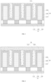
Fig. 2 to Fig. 4 are manufacturing process diagrams of the capacitor array structure according to an embodiment of the present disclosure; -
Fig. 5 and Fig. 6 are manufacturing process diagrams of the capacitor array structure according to another embodiment of the present disclosure; -
Fig. 7 is a schematic diagram of the reaction chamber according to an embodiment of the present disclosure. - Exemplary embodiments will now be described more fully with reference to the accompanying drawings. However, the exemplary embodiments could be implemented in many forms, and should not be construed as being limited to the embodiments set forth herein; on the contrary, these embodiments are provided in a way that makes the present disclosure more thorough and complete, and fully conveys the ideas of the exemplary embodiments to those skilled in the art.
- Furthermore, the described features, structures, or characteristics may be combined in any suitable manner in one or more embodiments. In the following description, numerous specific details are set forth in order to provide a thorough understanding of the embodiments of the present disclosure. However, those skilled in the art will realize that the technical solution of the present disclosure may be practiced without one or more of the specific details, or with other methods, devices, and steps, etc. In other cases, publicly known methods, devices, implementations, or operations are not shown or described in detail to avoid obscuring all aspects of the present disclosure.
- The flowcharts shown in the drawings are merely illustrative. Neither do they have to include all contents and steps nor do they have to be performed in the order described. For example, some steps may be broken down, and some may be combined or partially combined, so the actually applied order may be changed as the case may be. The terms "a," "an," and "the" are used to indicate the presence of one or more elements/components, etc. The terms "comprising", "including", and "having" are intended to be inclusive and mean that there may be additional elements/components, etc. besides those listed.
- An embodiment of the present disclosure provides a method for manufacturing a capacitor array structure, as shown in
Fig. 1 , the method for manufacturing a capacitor array structure comprises: - Step S100: providing a substrate;
- Step S200: forming a capacitor structure on the substrate; wherein the capacitor structure includes a bottom electrode layer formed on the substrate, a capacitor dielectric layer formed on a surface of the bottom electrode layer, and a top electrode layer formed on a surface of the capacitor dielectric layer; and there is gaps formed by the top electrode layer;
- Step S300: forming a filling layer to fill the gaps;
- Step S400: forming a covering layer to cover the filling layer and the top electrode layer;
- wherein the covering layer is combined with the filling layer to define a top electrode conductive layer; the material of both of the filling layer and the covering layer includes doped polycrystalline silicon; and the volume concentration of doped germanium atoms in the covering layer is greater than the volume concentration of doped germanium atoms in the filling layer.
- According to the method for manufacturing a capacitor array structure provided in the embodiments of the present disclosure, the top electrode conductive layer is formed by combining the filling layer and the covering layer, and the volume concentration of germanium atoms in the covering layer is greater than that of germanium atoms in the filling layer, so that the volume concentration of germanium atoms in the filling layer is relatively small, and the particle size of filling molecules is relatively reduced, so that the gaps can be filled more compactly; in the meanwhile, the volume concentration of germanium atoms in the covering layer is higher, so that the structural resistance can be balanced, and the performance of the top electrode conductive layer is ensured. By reducing the seam that appears when the top electrode conductive layer fills the gaps, the leakage current of the capacitor is reduced, and the performance of the capacitor is improved.
- Now, each step of the method for manufacturing a capacitor array structure in this exemplary embodiment will be further described.
- In Step S100, a substrate is provided.
- In some embodiments, as shown in
Fig. 2 , thesubstrate 10 comprises anunderlayer 110 and aninsulating layer 120, and a plurality of storagenode contact plugs 130 at interval are arranged in theinsulating layer 120. Wherein, theunderlayer 110 may be asemiconductor underlayer 110, and the material of thesemiconductor underlayer 110 may be silicon (Si), germanium (Ge), silicon germanium (GeSi), and silicon carbide (SiC), etc., which is not limited in the present disclosure. - Wherein, the
contact plugs 130 are used to connect thebottom electrode layer 210 of the capacitor formed subsequently, and data stored in a capacitor can be read or date can be written into a capacitor by thecontact plugs 130. The arrangement of themultiple contact plugs 130 is same as that of the capacitor holes subsequently formed. In an embodiment, themultiple contact plugs 130 may be arranged in a hexagonal array. Wherein, thecontact plugs 130 are made of a metal, which may be W (tungsten), Cu (copper), Ti (titanium), Ni (nickel) or Al (aluminum), or metal silicide. Thecontact plugs 130 may be formed by depositing and then etching a conducting layer, or by an electroplating process. - Wherein, the material of the
insulating layer 120 may be silicon oxide, silicon nitride, or any other suitable material, and the material of theinsulating layer 120 may be a single-layer or multi-layer stacked structure. In an embodiment, theinsulating layer 120 is formed as follows: an insulating material layer is formed on thesemiconductor underlayer 110 by deposition process, and the insulating material layer covers thecontact plugs 130, wherein the deposition process can be chemical vapor deposition, plasma enhanced chemical vapor deposition or low pressure chemical vapor deposition; the insulating material layer on the surface of thecontact plugs 130 is removed by flattening process to form theinsulating layer 120, wherein the flattening process may be a chemical mechanical grinding process. - In Step S200, a capacitor structure is formed on the substrate, the capacitor structure includes a bottom electrode layer formed on the substrate, a capacitor dielectric layer formed on the surface of the bottom electrode layer, and a top electrode layer formed on the surface of the capacitor dielectric layer, and there is gaps formed by the top electrode layer.
- In some embodiments, as shown in
Fig. 2 , acapacitor structure 20 is formed on the substrate; the capacitor structure includes abottom electrode layer 210 formed on thesubstrate 10, a capacitordielectric layer 220 formed on the surface of thebottom electrode layer 210, and atop electrode layer 230 formed on the surface of the capacitordielectric layer 220. - Wherein, a
bottom electrode layer 210 comprising a plurality of pillar-shaped electrodes is formed by atomic layer deposition or chemical vapor deposition or physical vapor deposition. Wherein, the material of thebottom electrode layer 210 may include one of tungsten, titanium, nickel, aluminum, platinum, titanium nitride, N-type polysilicon, P-type polysilicon, or a stack of two or more of the above materials; and the material of the bottom electrode layer may further include a metal nitride or a metal silicide, or a compound of metal nitride and metal silicide, such as titanium nitride, titanium silicide, nickel silicide, and titanium silicon nitride (TiSixNy). In an embodiment, the material of thebottom electrode layer 210 is same as the material of thecontact plugs 130, so that the bottom electrode formed by thebottom electrode layer 210 and thecontact plugs 130 has good electrical properties. - Wherein, a capacitor
dielectric layer 220 covering thebottom electrode layer 210 may be formed by atomic layer deposition, chemical vapor deposition, or physical vapor deposition, and the capacitordielectric layer 220 simultaneously covers the surface of thesubstrate 10 exposed from a plurality of columnar electrodes. When there is no other film layer between the capacitordielectric layer 220 and thebottom electrode layer 210, the capacitordielectric layer 220 may directly cover the surface of thebottom electrode layer 210; when any other film layer is involved between the capacitordielectric layer 220 and thebottom electrode layer 210, the dielectric layer is not in direct contact with thebottom electrode layer 210, but covers thebottom electrode layer 210 relatively. Wherein, the capacitordielectric layer 220 may be a single-layer or multi-layer stacked structure, and the capacitordielectric layer 220 may be one of a stacked structure composed of strontium titanate and titanium oxide (SrTiO3/TiO2), a stacked structure composed of aluminum oxide and hafnium oxide (AlO/HfO), a stacked structure composed of zirconium oxide and aluminum oxide (ZrO/AlO/ZrO), and a composite perovskite-type ferroelectric material (a BST material, a ferroelectric material with a composite perovskite structure, a solid solution composed of BaTiO3 and SrTiO3 at a certain ratio); the capacitor dielectric layer may also be formed using silicon oxide, silicon nitride, silicon oxynitride, FSG (fluorine doped silicon dioxide), BSG (boron doped silicon dioxide), PSG (phosphorus doped silicon dioxide), or BPSG (boron phosphorus doped silicon dioxide), or a combination thereof. The dielectric constant of the capacitordielectric layer 220 is between 4 and 400, and the capacitordielectric layer 220 is preferably made of a high-K dielectric material to increase the capacitance per unit area of the capacitor. - Wherein, a
top electrode layer 230 comprising a plurality of columnar electrodes is formed by atomic layer deposition or chemical vapor deposition or physical vapor deposition. Wherein, the material that forms thetop electrode layer 230 may include one of tungsten, titanium, nickel, aluminum, platinum, titanium nitride, N-type polysilicon, P-type polysilicon, or a stack of two or more of the above materials, and may further include a metal nitride or a metal silicide, or a compound of metal nitride and metal silicide, such as titanium nitride, titanium silicide, nickel silicide and titanium silicon nitride (TiSixNy). In an embodiment, the material of thetop electrode layer 230 is same as the material of thebottom electrode layer 210 to reduce process difficulty and improve process efficiency. - As shown in
Fig. 2 , after thetop electrode layer 230 covers the capacitordielectric layer 220, there is gaps formed by thetop electrode layer 230 of adjacent columnar electrodes, and the gaps have a large depth-to-width ratio (20:1 ~ 100:1); for example, the height may be 1000nm ~ 2000nm, and the CD (critical dimension) may be 30nm ~ 60nm. In the conventional method, when the gaps of the top electrode layer are filled, sealing in advance would occur, which forms seams in the top electrode conductive layer, and increases the leakage current of the capacitor array structure. - In Step S300, a filling layer is formed to fill the gaps.
- In some embodiments, as shown in
Fig. 3 andFig. 7 , afilling layer 310 filling the gaps may be formed by chemical vapor deposition in the reaction chamber 90. The material of thefilling layer 310 includes germanium-doped polysilicon doped with germanium atoms, and SiH4 gas and GeH4 gas are introduced by a nozzle. The chemical reaction of SiH4 gas and GeH4 gas in the reaction chamber 90 is as follows:
SiH4 ( g ) →Si ( s ) +2H2 ( g )
GeH4 ( g ) →Ge ( s ) + 2H2 ( g )
- When SiH4 gas and GeH4 gas are introduced into the reaction chamber 90, Si atoms and Ge atoms are generated by chemical reaction, and Si atoms and Ge atoms are deposited in the gaps to form a
filling layer 310 with germanium-doped polysilicon. - Wherein, when the
filling layer 310 is deposited by chemical vapor deposition in the reaction chamber 90, SiH4 gas is introduced at a flow rate of 300 sccm ~ 700 sccm and GeH4 gas is introduced at a flow rate of 850 sccm ~ 1300 sccm. When the flow rate of GeH4 gas is set to the above standard milliliters/minute, a good deposition effect of the deposition material can be ensured, and the seams in thefilling layer 310 is further reduced. Of course, the flow rates of SiH4 gas and GeH4 gas may be out of the above ranges, and which are not restricted by the present disclosure. - Wherein, the duration time of introducing SiH4 gas and GeH4 gas into the reaction chamber 90 is 20 min ~ 50 min, such as 20 min, 30 min, 40 min, or 50 min. Of course; the deposition time may be greater than 20 min or less than 50 min, the specific deposition time can be set according to the actual situation of gaps filling, and which is not restricted by the present disclosure.
- For example, the material of the
filling layer 310 may be germanium-boron co-doped polysilicon, and SiH4 gas, GeH4 gas, and BCl3 gas may be simultaneously introduced by a nozzle, wherein the chemical reaction of BCl3 gas in the reaction chamber 90 is as follows:
2BCl3 ( g ) →2B ( s ) + 3Cl2 ( g )
- When SiH4 gas, GeH4 gas, and BCl3 gas are introduced into the reaction chamber 90, Si atoms, B atoms, and Ge atoms are generated by chemical reaction and deposited the gaps of the
filling layer 310, to fill the gaps. Wherein, when thefilling layer 310 is deposited by chemical vapor deposition in the reaction chamber 90, the flow rate of BCl3 gas introduced is 500 sccm ~ 200 sccm. Of course, the gas flow rate of BCl3 may be out of the above range, and which is not restricted by the present disclosure. Wherein, the duration time for introducing BCl3 gas into the reaction chamber 90 is 20 min ~ 50 min, such as 20 min, 30 min, 40 min, or 50 min. Of course, the deposition time may be greater than 20 min or less than 50 min, the specific deposition time can be set according to the actual situation of gaps filling, and which is not restricted by the present disclosure. Wherein, the duration times for introducing SiH4 gas, GeH4 gas, and BCl3 gas can be same, so that the uniformity of deposition of various atoms in germanium-boron co-doped polycrystalline silicon is improved, and the conductivity of the top electrode conductive layer is improved. - As shown in
Fig. 3 , the depth-to-width ratio of the gaps is 20:1 ~ 100:1, thefilling layer 310 completely fills the gaps, and afilling layer 310 at a certain thickness is also formed on one side surface of thetop electrode layer 230 away from thesubstrate 10. As shown inFig. 5 , thefilling layer 310 only completely fills the gaps, and the material of thefilling layer 310 is not formed on the surface of one side of thetop electrode layer 230 away from thesubstrate 10, in order to expose the surface of one side of thetop electrode layer 230 which is far away from thesubstrate 10, and thecovering layer 320 is also exposed. The volume concentration of germanium atoms in thecovering layer 320 is greater than the volume concentration of the germanium atoms in thefilling layer 310, and the conductive layer is good, so that the conductivity of the top electrodeconductive layer 30 can be improved. Of course, thefilling layer 310 may also partially fill the gaps, which is not restricted by the present disclosure. - Wherein, during chemical vapor deposition, the temperature in the reaction chamber 90 is 300 °C ~ 600 °C, such as 300 °C, 400°C, 500 °C, and 600 °C. Of course, during chemical vapor deposition, the temperature in the reaction chamber 90 may also be less than 300°C or greater than 600°C, and which is not restricted by the present disclosure. Wherein, during chemical vapor deposition, the pressure in the reaction chamber 90 is 100 mtorr ~ 600 mtorr, such as 100 mtorr, 200 mtorr, 300 mtorr, 400 mtorr, 500 mtorr, or 600 mtorr. Of course, during chemical vapor deposition, the pressure in the reaction chamber 90 may also be less than 100 mtorr or greater than 600 mtorr, and which is not restricted by the present disclosure.
- By using the
filling layer 310 with a relatively low volume concentration of germanium atoms, the particle size of the filling material is relatively reduced, so that the gaps can be filled more compactly, the size of the seams formed is reduced when germanium-boron co-doped polycrystalline silicon is filled in the gaps, the leakage current of the capacitor is reduced, and the performance of the capacitor is improved. - In Step S400, a covering layer is formed to cover the filling layer and the top electrode layer; wherein, the covering layer is combined with the filling layer to form a top electrode conductive layer; the material of both of the filling layer and the covering layer includes doped polycrystalline silicon, and the volume concentration of doped germanium atoms in the covering layer is greater than the volume concentration of doped germanium atoms in the filling layer.
- In some embodiments, as shown in
Fig. 4 ,Fig. 6 andFig. 7 , acovering layer 320 covering both of thefilling layer 310 and thetop electrode layer 230 may be formed in the reaction chamber 90 by chemical vapor deposition; thecovering layer 320 and thefilling layer 310 may be formed in the same reaction chamber 90 to reduce process difficulty and improve process efficiency. The material of thecovering layer 320 includes germanium-doped polysilicon doped with germanium atoms, and SiH4 gas and GeH4 gas are introduced by a nozzle. The chemical reaction of the SiH4 gas and GeH4 gas in the reaction chamber 90 is as follows:
SiH4 ( g ) →Si ( s ) +2H2 ( g )
GeH4 ( g ) →Ge ( s ) + 2Hz ( g )
- When SiH4 gas and GeH4 gas have been introduced into the reaction chamber 90, and Si atoms and Ge atoms are generated by chemical reaction, and Si atoms and Ge atoms are deposited in the gaps to form a
covering layer 320 of germanium-doped polysilicon. - Wherein, when the
covering layer 320 is deposited by chemical vapor deposition in the reaction chamber 90, SiH4 gas is introduced at a flow rate of 300 sccm ~ 700 sccm, and GeH4 gas is introduced at a flow rate of 1250 sccm ~ 1800 sccm; when the flow rate of GeH4 gas is set to the above standard milliliters/minute, the volume concentration of germanium atoms can be ensured, and thecovering layer 320 formed has excellent conductivity. Of course, the flow rates of SiH4 gas and GeH4 gas may be out of the above ranges, and which are not restricted by the present disclosure. - Wherein, the duration time of introducing SiH4 gas and GeH4 gas into the reaction chamber 90 is 120 min ~ 180 min, such as 120 min, 130 min, 140 min, 150 min, 160 min, 170 min, or 180 min. Of course, the deposition time may also be less than 120 min or greater than 180 min, to be set based on the actual thickness of the
covering layer 320, etc., and which is not restricted by the present disclosure. - For example, the material of the
covering layer 320 may be germanium-boron co-doped polysilicon, and SiH4 gas, GeH4 gas and BCl3 gas may be simultaneously introduced by a nozzle, wherein the chemical reaction of BCl3 gas in the reaction chamber 90 is as follows:
2BCl3 ( g ) →2B (s) + 3Cl2 ( g )
- When SiH4 gas, GeH4 gas and BCl3 gas are introduced into the reaction chamber 90, Si atoms , B atoms and Ge atoms are generated by chemical reaction and deposited on the filling layer and the top electrode layer to form a
covering layer 320 of Ge-B co-doped polysilicon, so that thefilling layer 310 and thetop electrode layer 230 are covered. When thecovering layer 320 is deposited by chemical vapor deposition in the reaction chamber 90, the flow rate of BCl3 gas introduced is 500 sccm ~ 200 sccm. Of course, the gas flow rate of BCl3 may be out of the above range, and which is not restricted by the present disclosure. The duration time of introducing BCl3 gas into the reaction chamber 90 is 120 min-180 min, such as 120 min, 130 min, 140 min, 150 min, 160 min, 170 min, or 180 min. Of course, the deposition time may also be shorter than 120 min or greater than 180 min, to be set based on the actual thickness of thecovering layer 320, etc., and which is not restricted by the present disclosure. Wherein, the times for introducing SiH4 gas, the GeH4 gas and the BCl3 gas can be the same, so that the uniformity of deposition of various atoms in germanium-boron co-doped polycrystalline silicon is improved, and the conductivity of the top electrode conductive layer is improved. - Wherein, during chemical vapor deposition, the temperature in the reaction chamber 90 is 300 °C ~ 600 °C, such as 300 °C, 400°C, 500 °C, and 600 °C. Of course, during chemical vapor deposition, the temperature in the reaction chamber 90 may also be less than 300°C or greater than 600°C, and which is not restricted by the present disclosure. Wherein, during chemical vapor deposition, the pressure in the reaction chamber 90 is 100 mtorr ~ 600 mtorr, such as 100 mtorr, 200 mtorr, 300 mtorr, 400 mtorr, 500 mtorr, or 600 mtorr. Of course, during chemical vapor deposition, the pressure in the reaction chamber 90 may also be less than 100 mtorr or greater than 600 mtorr, and which is not restricted by the present disclosure.
- In the reaction chamber 90, the temperature and the pressure during forming the
covering layer 320 are respectively same as the temperature and the pressure during forming thefilling layer 310, which can reduce process difficulty and improve process efficiency. Of course, in the reaction chamber 90, the temperature and the pressure during forming thecovering layer 320 may be same as or be different to the temperature and the pressure during forming thefilling layer 310,, and which are not restricted by the present disclosure. - The volume concentration of germanium atoms in the
covering layer 320 is greater than 30% ~ 50% of that of the germanium atoms in thefilling layer 310. When the volume concentration of germanium atoms in thecovering layer 320 is greater than that of the germanium atoms in thefilling layer 310, the resistance of thecovering layer 320 is low, and thecovering layer 320 located outside the gaps has good conductivity, so that the conductivity of the top electrodeconductive layer 30 can be improved and the situation that the conductivity of the top electrodeconductive layer 30 is affected due to the low volume concentration of germanium atoms in thefilling layer 310 is avoided. - The device embodiments of the present disclosure are as follow, The device embodiments may be manufactured by the method embodiments described above. Please refer to the relevant discussion of the method embodiments for details not disclosed in the device embodiment.
- The embodiments of the present disclosure also provide a capacitor array structure, as shown in
Fig. 2 to Fig. 6 . The capacitor array structure comprises asubstrate 10, acapacitor structure 20, and a top electrodeconductive layer 30. Thecapacitor structure 20 is arranged on thesubstrate 10, and thecapacitor structure 20 comprises abottom electrode layer 210, acapacitor dielectric layer 220 and atop electrode layer 230. Thecapacitor dielectric layer 220 covers the surface of thebottom electrode layer 210, thetop electrode layer 230 covers the surface of thecapacitor dielectric layer 220, and there is gaps formed in thetop electrode layer 230. The top electrodeconductive layer 30 comprises afilling layer 310 and acovering layer 320; thefilling layer 310 fills the gaps, thecovering layer 320 covers thefilling layer 310 and thetop electrode layer 230; the material of thecovering layer 320 and thefilling layer 310 includes doped polysilicon; and the volume concentration of germanium atoms doped in thecovering layer 320 is greater than that of germanium atoms doped in thefilling layer 310. - In the capacitor array structure provided in the present disclosure, the top electrode
conductive layer 30 is formed by combining thefilling layer 310 and thecovering layer 320, and the volume concentration of the germanium atoms in thecovering layer 320 is greater than that of germanium atoms in thefilling layer 310, so that the volume concentration of germanium atoms in thefilling layer 310 is relatively low, and the particle size of filling molecules is relatively reduced, so that the gaps can be filled more concentrated. In the meanwhile, when the volume concentration of the germanium atoms in thecovering layer 320 is higher, the resistance of the structural can be balanced, and the performance of the top electrodeconductive layer 30 is ensured. By reducing the seam that appears when the top electrodeconductive layer 30 fills the gaps, the leakage current of the capacitor is reduced, and the performance of the capacitor is improved. - In some embodiments, as shown in
Fig. 3 andFig. 7 , afilling layer 310 filling the gaps may be formed by chemical vapor deposition in the reaction chamber 90. - The material of the
filling layer 310 includes germanium-doped polysilicon doped with germanium atoms, and SiH4 gas and GeH4 gas are introduced by a nozzle. The chemical reaction of SiH4 gas and GeH4 gas introduced in the reaction chamber 90 is as follows:
SiH4 ( g ) →Si ( s ) +2H2 ( g )
GeH4 ( g ) →Ge ( s ) + 2Hz ( g )
- For example, the material of the
filling layer 310 may be germanium-boron co-doped polysilicon, and SiH4 gas, GeH4 gas, and BCl3 gas may be simultaneously introduced by a nozzle, wherein the chemical reaction of BCl3 gas in the reaction chamber 90 is as follows:
2BCl3 ( g ) →2B ( s ) + 3Cl2 ( g )
- SiH4 gas, GeH4 gas, and BCl3 gas are introduced in the reaction chamber 90, Si atoms, B atoms, and Ge atoms are generated by a chemical reaction, and Si atoms, B atoms, and Ge atoms are deposited on the
filling layer 310 in the gaps to fill the gaps. - When the
filling layer 310 is deposited by chemical vapor deposition in the reaction chamber 90, SiH4 gas is introduced at a flow rate of 300 sccm ~ 700 sccm, GeH4 gas is introduced at a flow rate of 850 sccm ~ 1300 sccm, and BCl3 gas is introduced at a flow rate of 500 sccm ~ 200 sccm. When the flow rates of SiH4 gas, GeH4 gas, and BCl3 gas are set to the above standard milliliters/minute, a good deposition effect of the deposition material can be ensured, and the seam in thefilling layer 310 is further reduced. Of course, the flow rates of SiH4 gas, the GeH4 gas and the BCl3 gas may be out of the above ranges, and which are not restricted by the present disclosure. The volume concentration of germanium atoms in thefilling layer 310 is 45% ~ 80%, such as 45%, 50%, 55%, 65%, 70%, 75%, or 80%. - As shown in
Fig. 3 , thefilling layer 310 completely fills the gaps, and afilling layer 310 at a certain thickness is also formed on the surface of one side of thetop electrode layer 230 away from thesubstrate 10. As shown inFig. 5 , thefilling layer 310 only completely fills the gaps, and the material of thefilling layer 310 is not formed on the surface of one side of thetop electrode layer 230 away from thesubstrate 10, in order to expose the surface of one side of thetop electrode layer 230 away from thesubstrate 10 and thecovering layer 320. The volume concentration of germanium atoms in thecovering layer 320 is greater than that of the germanium atoms in thefilling layer 310, and the conductive layer is good, so that the conductivity of the top electrodeconductive layer 30 can be improved. Of course, thefilling layer 310 may also partially fill the gaps, which is not restricted by the present disclosure. - Wherein, during chemical vapor deposition, the temperature in the reaction chamber 90 is 300 °C ~ 600 °C, such as 300 °C, 400°C, 500 °C, and 600 °C. Of course, during chemical vapor deposition, the temperature in the reaction chamber 90 may also be less than 300°C or greater than 600°C, and which is not restricted by the present disclosure. Wherein, during chemical vapor deposition, the pressure in the reaction chamber 90 is 100 mtorr ~ 600 mtorr, such as 100 mtorr, 200 mtorr, 300 mtorr, 400 mtorr, 500 mtorr, or 600 mtorr. Of course, during chemical vapor deposition, the pressure in the reaction chamber 90 may also be less than 100 mtorr or greater than 600 mtorr, and which is not restricted by the present disclosure. The deposition time of the
filling layer 310 in the reaction chamber 90 by chemical vapor deposition is 20 min ~ 50 min, such as 20 min, 30 min, 40 min, or 50 min. Of course, the deposition time may be greater than 20 min or shorter than 50 min, to be set according to the actual situation of gaps filling, and which is not restricted by the present disclosure. - As shown in
Fig. 4 ,Fig. 6 , andFig. 7 , acovering layer 320 covering thefilling layer 310 and thetop electrode layer 230 may be formed in the reaction chamber 90 by chemical vapor deposition, and thecovering layer 320 and thefilling layer 310 may be formed in the same reaction chamber 90 to reduce process difficulty and improve process efficiency. SiH4 gas, the GeH4 gas and the BCl3 gas are introduced into the reaction chamber 90, Si atoms, B atoms, and Ge atoms are generated by chemical reaction, and Si atoms, B atoms, and Ge atoms are deposited on thefilling layer 310 in the gaps to cover thefilling layer 310 and thetop electrode layer 230. - When the
filling layer 310 is deposited by chemical vapor deposition in the reaction chamber 90, SiH4 gas is introduced at a flow rate of 300 sccm ~ 700 sccm, GeH4 gas is introduced at a flow rate of 1,250 sccm ~ 1,800 sccm, and BCl3 gas is introduced at a flow rate of 500 sccm ~ 200 sccm. When the flow rates of SiH4 gas, the GeH4 gas and the BCl3 gas are set to the above standard milliliters/minute, a good deposition effect of the deposition material can be ensured, and the seam in thefilling layer 310 is further reduced. Of course, the flow rates of SiH4 gas, the GeH4 gas and the BCl3 gas may be out of the above ranges, and which are not restricted by the present disclosure. The volume concentration of germanium atoms in thecovering layer 320 is 55% ~ 85%, such as 55%, 60%, 65%, 75%, 80%, or 85%; the volume concentration of germanium atoms in thecovering layer 320 is greater than 30% ~ 50% of that of the germanium atoms in thefilling layer 310, such as 30%, 35%, 40%, 45%, or 50%. - Since the gaps has a large depth-to-width ratio (20:1 ~ 100:1), by using the
filling layer 310 with a relatively low volume concentration of germanium atoms, the particle size of the filling material is relatively reduced, so that the gaps can be filled more compactly, the size of the seam that appears when germanium-boron co-doped polycrystalline silicon is filled in the gaps is reduced, the leakage current of the capacitor is reduced, and the performance of the capacitor is improved. When the volume concentration of germanium atoms in thecovering layer 320 is greater than that of the germanium atoms in thefilling layer 310, the resistance of thecovering layer 320 is low, and thecovering layer 320 located outside the gaps has good conductivity, so that the conductivity of the top electrodeconductive layer 30 can be improved as a whole, and the situation that the conductivity of the top electrodeconductive layer 30 is affected due to the low volume concentration of germanium atoms in thefilling layer 310 is avoided. - In some embodiments, as shown in
Fig. 2 , thesubstrate 10 comprises anunderlayer 110 and an insulatinglayer 120, and a plurality of storage node contact plugs 130 arranged alternatively are disposed in the insulatinglayer 120. Wherein, theunderlayer 110 may be asemiconductor underlayer 110, and the material of thesemiconductor underlayer 110 may be silicon (Si), germanium (Ge), silicon germanium (GeSi), and silicon carbide (SiC), etc., which is not limited in the present disclosure. - Wherein, the contact plugs 130 are used to connect the
bottom electrode layer 210 of the capacitor formed subsequently, and data can be read from or written into the capacitor by the contact plugs 130. The arrangement of the multiple contact plugs 130 is same as that of the capacitor holes formed subsequently. In an embodiment, the multiple contact plugs 130 may be arranged in a hexagonal array. Wherein, the contact plugs 130 are made of a metal, which may be W (tungsten), Cu (copper), Ti (titanium), Ni (nickel) or Al (aluminum), or metal silicide. The contact plugs 130 may be formed by depositing and then etching a conducting layer, or by an electroplating process. - Wherein, the material of the insulating
layer 120 may be silicon oxide, silicon nitride, or any other suitable material, and the material of the insulatinglayer 120 may be a single-layer or multi-layer stacked structure. In an embodiment, the insulatinglayer 120 is formed as follows: an insulating material layer is formed on thesemiconductor underlayer 110 by deposition, and covers the contact plugs 130, wherein the deposition process can be chemical vapor deposition, plasma enhanced chemical vapor deposition or low pressure chemical vapor deposition; the insulating material layer on the surface of the contact plugs 130 is removed by flattening to form the insulatinglayer 120, wherein the flattening process may be a chemical mechanical grinding process. - The
capacitor structure 20 comprises abottom electrode layer 210, acapacitor dielectric layer 220 and a top electrode layer 230.The material of thebottom electrode layer 210 may include one of tungsten, titanium, nickel, aluminum, platinum, titanium nitride, N-type polysilicon, P-type polysilicon, or a stack of two or more of the above materials, and may further include a metal nitride or metal silicide, or a compound of both, such as titanium nitride, titanium silicide, nickel silicide, and titanium silicon nitride (TiSixNy). In an embodiment, the material of thebottom electrode layer 210 is same as that of the contact plugs 130, so that the bottom electrode formed by thebottom electrode layer 210 and the contact plugs 130 has good electrical properties. - Wherein, the
capacitor dielectric layer 220 may be a single-layer or multi-layer stacked structure, and thecapacitor dielectric layer 220 may be one of a stacked structure composed of strontium titanate and titanium oxide (SrTiO3/TiO2), a stacked structure composed of aluminum oxide and hafnium oxide (AlO/HfO), a stacked structure composed of zirconium oxide and aluminum oxide (ZrO/AlO/ZrO), and a composite perovskite-type ferroelectric material (a BST material, a ferroelectric material with a composite perovskite structure, a solid solution composed of BaTiO3 and SrTiO3 at a certain ratio); it may also be made of a material comprising one or more of silicon oxide, silicon nitride, silicon oxynitride, FSG (fluorine doped silicon dioxide), BSG (boron doped silicon dioxide), PSG (phosphorus doped silicon dioxide), and BPSG (boron phosphorus doped silicon dioxide). The dielectric constant of thecapacitor dielectric layer 220 is between 4 and 400, and thecapacitor dielectric layer 220 is preferably made of a high-K dielectric material to increase the capacitance per unit area of the capacitor. - Wherein, the material of the
top electrode layer 230 may include one of tungsten, titanium, nickel, aluminum, platinum, titanium nitride, N-type polysilicon, P-type polysilicon, or a stack of two or more of the above materials, and the material of the top electrode layer may further include a metal nitride or metal silicide, or a compound of both, such as titanium nitride, titanium silicide, nickel silicide and titanium silicon nitride (TiSixNy). In an embodiment, the material of thetop electrode layer 230 is same as that of thebottom electrode layer 210 to reduce process difficulty and improve process efficiency. - The embodiments of the present disclosure also provide a semiconductor memory device. The semiconductor memory device comprises the capacitor array structure above, the substrate further comprises a transistor, and the capacitor structure is electrically connected to the transistor; the capacitor array structure can be formed by the method for manufacturing a capacitor array structure. For the advantageous effects of the semiconductor memory device, reference is made to the above discussion of the capacitor array structure, which is not repeated here. As an example, the semiconductor memory device may be, but is not limited to, a dynamic random access memory (DRAM).
- Those skilled in the art can easily think of other embodiments of the present disclosure when considering the specification and practicing the invention disclosed herein. The present application is intended to cover any variants, uses, or adaptations of the present disclosure following the general principles of the present disclosure and including common knowledge or customary technical means in the art not disclosed in the present disclosure. The specification and the embodiments are deemed exemplary only, and the true scope and spirit of the present disclosure are indicated by the following claims.
- It should be understood that the present disclosure is not limited to the precise structures that have been described above and shown in the drawings, and that various modifications and changes may be made without departing from the scope thereof. The scope of the present disclosure is restricted by the attached claims only.
Claims (15)
- A method for manufacturing a capacitor array structure, comprising:providing a substrate;forming a capacitor structure on the substrate; wherein the capacitor structure comprises a bottom electrode layer formed on the substrate, a capacitor dielectric layer formed on a surface of the bottom electrode layer, and a top electrode layer formed on a surface of the capacitor dielectric layer; and there is gaps formed by the top electrode layer;forming a filling layer to fill the gaps;forming a covering layer to cover the filling layer and the top electrode layer;wherein, the covering layer is combined with the filling layer to define a top electrode conductive layer; a material of both of the filling layer and the covering layer comprises doped polycrystalline silicon; and a volume concentration of doped germanium atoms in the covering layer is greater than a volume concentration of doped germanium atoms in the filling layer.
- The method for manufacturing a capacitor array structure according to claim 1, wherein the filling layer and the covering layer are formed by chemical vapor deposition.
- The method for manufacturing a capacitor array structure according to claim 2, wherein GeH4 gas is introduced when the filling layer is formed;
a flow rate of GeH4 gas introduced is 850 sccm ~ 1300 sccm. - The method for manufacturing a capacitor array structure according to claim 3, wherein a duration time of GeH4 gas introduced is 20 min ~ 50 min.
- The method for manufacturing a capacitor array structure according to claim 2, wherein GeH4 gas is introduced when the covering layer is formed;
a flow rate of GeH4 gas introduced is 1250 sccm ~ 1800 sccm. - The method for manufacturing a capacitor array structure according to claim 5, wherein a duration time of GeH4 gas introduced is 120 min ~ 180 min.
- The method for manufacturing a capacitor array structure according to claim 1, wherein a volume concentration of germanium atoms in the covering layer is greater than 30% - 50% of a volume concentration of germanium atoms in the filling layer.
- The method for manufacturing a capacitor array structure according to claim 2, wherein, during a chemical vapor deposition, a temperature is 300°C ~ 600°C.
- The method for manufacturing a capacitor array structure according to claim 2, wherein, during a chemical vapor deposition, a pressure in a reaction chamber is 100 mtorr ~ 600 mtorr.
- The method for manufacturing a capacitor array structure according to claim 2, wherein, when the filling layer and the covering layer are formed, GeH4 gas, SiH4 gas, and BCl3 gas are simultaneously introduced;
a flow rate of SiH4 gas introduced is 300 sccm ~ 700 sccm, and a flow rate of BCl3 gas introduced is 50 sccm ~ 200 sccm. - A capacitor array structure, comprising:a substrate;a capacitor structure, arranged on the substrate; wherein the capacitor structure comprises a bottom electrode layer, a capacitor dielectric layer and a top electrode layer; the capacitor dielectric layer covers a surface of the bottom electrode layer; the top electrode layer covers a surface of the capacitor dielectric layer; and there is gaps formed by the top electrode layer;an top electrode conductive layer, comprising a filling layer and a covering layer; wherein the filling layer fills the gaps, the covering layer covers the filling layer and the top electrode layer; a material of both of the covering layer and the filling layer comprises doped polycrystalline silicon; and a volume concentration of doped germanium atoms in the covering layer is greater than a volume concentration of doped germanium atoms in the filling layer.
- The capacitor array structure according to claim 11, wherein the volume concentration of germanium atoms in the covering layer is greater than 30% ~ 50% of the volume concentration of the germanium atoms in the filling layer.
- The capacitor array structure according to claim 11, wherein the volume concentration of germanium atoms in the filling layer is 45% ~ 80%, and the volume concentration of germanium atoms in the covering layer is 55% ~ 85%.
- The capacitor array structure according to claim 11, wherein the filling layer fills at least the gaps, and a depth-to-width ratio of the gaps is 20:1 ~ 100:1.
- A semiconductor memory device, comprising a capacitor array structure according to any one of claims 11 to 14; wherein, the substrate further comprises a transistor; and the capacitor structure is electrically connected to the transistor.
Applications Claiming Priority (2)
| Application Number | Priority Date | Filing Date | Title |
|---|---|---|---|
| CN202011068522.7A CN114284216B (en) | 2020-09-28 | 2020-09-28 | Capacitor array structure and manufacturing method thereof and semiconductor memory device |
| PCT/CN2021/103744 WO2022062545A1 (en) | 2020-09-28 | 2021-06-30 | Capacitor array structure, manufacturing method therefor, and semiconductor storage device |
Publications (2)
| Publication Number | Publication Date |
|---|---|
| EP4199086A1 true EP4199086A1 (en) | 2023-06-21 |
| EP4199086A4 EP4199086A4 (en) | 2024-02-14 |
Family
ID=80846194
Family Applications (1)
| Application Number | Title | Priority Date | Filing Date |
|---|---|---|---|
| EP21870924.4A Pending EP4199086A4 (en) | 2020-09-28 | 2021-06-30 | CAPACITOR ARRAY STRUCTURE, MANUFACTURING METHOD THEREFOR AND SEMICONDUCTOR STORAGE DEVICE |
Country Status (4)
| Country | Link |
|---|---|
| US (1) | US11411071B1 (en) |
| EP (1) | EP4199086A4 (en) |
| CN (1) | CN114284216B (en) |
| WO (1) | WO2022062545A1 (en) |
Families Citing this family (2)
| Publication number | Priority date | Publication date | Assignee | Title |
|---|---|---|---|---|
| CN116133436A (en) * | 2021-11-12 | 2023-05-16 | 联华电子股份有限公司 | Semiconductor element and manufacturing method thereof |
| CN116056558B (en) * | 2023-03-28 | 2023-08-29 | 长鑫存储技术有限公司 | Manufacturing method of semiconductor structure and structure thereof |
Family Cites Families (16)
| Publication number | Priority date | Publication date | Assignee | Title |
|---|---|---|---|---|
| TW420871B (en) * | 1999-01-08 | 2001-02-01 | Taiwan Semiconductor Mfg | Process for improving the characteristics of stack capacitors |
| KR100363083B1 (en) * | 1999-01-20 | 2002-11-30 | 삼성전자 주식회사 | Hemispherical grain capacitor and forming method thereof |
| KR20010059517A (en) * | 1999-12-30 | 2001-07-06 | 박종섭 | Method for forming cylinder type bottom electrode intergrated memory device |
| KR100393208B1 (en) * | 2001-01-15 | 2003-07-31 | 삼성전자주식회사 | Semiconductor device using doped polycrystalline silicon-germanium layer and method for manufacturing the same |
| KR100618869B1 (en) * | 2004-10-22 | 2006-09-13 | 삼성전자주식회사 | Semiconductor device including capacitor and method for manufacturing same |
| KR100655691B1 (en) * | 2005-09-21 | 2006-12-08 | 삼성전자주식회사 | Capacitors and methods of making the same. |
| KR20080018685A (en) * | 2006-08-25 | 2008-02-28 | 삼성전자주식회사 | Semiconductor wiring structure, semiconductor device including capacitor and manufacturing method thereof |
| CN100508209C (en) | 2007-08-01 | 2009-07-01 | 中电华清微电子工程中心有限公司 | NPN-type germanium-silicon heterojunction bipolar transistor and manufacturing method thereof |
| US8629426B2 (en) | 2010-12-03 | 2014-01-14 | Taiwan Semiconductor Manufacturing Company, Ltd. | Source/drain stressor having enhanced carrier mobility manufacturing same |
| CN105374684A (en) | 2014-08-30 | 2016-03-02 | 中芯国际集成电路制造(上海)有限公司 | PMOS structure and formation method thereof |
| US9431551B2 (en) | 2014-09-15 | 2016-08-30 | Infineon Technologies Ag | Circuit arrangement and method of forming a circuit arrangement |
| CN207398140U (en) * | 2017-11-07 | 2018-05-22 | 睿力集成电路有限公司 | Array of capacitors structure |
| CN107910327B (en) * | 2017-11-07 | 2024-05-14 | 长鑫存储技术有限公司 | Capacitor array structure and manufacturing method thereof |
| CN107968044B (en) * | 2017-12-19 | 2024-02-09 | 长鑫存储技术有限公司 | Capacitor array structure, semiconductor memory and preparation method |
| CN108155152B (en) * | 2017-12-19 | 2019-09-06 | 长鑫存储技术有限公司 | Conductor structure, capacitor array structure and preparation method |
| US11075204B2 (en) | 2018-12-14 | 2021-07-27 | Xia Tai Xin Semiconductor (Qing Dao) Ltd. | Semiconductor device and method for fabricating the same |
-
2020
- 2020-09-28 CN CN202011068522.7A patent/CN114284216B/en active Active
-
2021
- 2021-06-30 EP EP21870924.4A patent/EP4199086A4/en active Pending
- 2021-06-30 US US17/599,464 patent/US11411071B1/en active Active
- 2021-06-30 WO PCT/CN2021/103744 patent/WO2022062545A1/en not_active Ceased
Also Published As
| Publication number | Publication date |
|---|---|
| EP4199086A4 (en) | 2024-02-14 |
| US11411071B1 (en) | 2022-08-09 |
| WO2022062545A1 (en) | 2022-03-31 |
| CN114284216B (en) | 2024-09-13 |
| CN114284216A (en) | 2022-04-05 |
Similar Documents
| Publication | Publication Date | Title |
|---|---|---|
| JP6943922B2 (en) | Semiconductor memory element | |
| US7799631B2 (en) | Multiple-layer dielectric layer and method for fabricating capacitor including the same | |
| US8575680B2 (en) | Semiconductor device having air gap and method of fabricating the same | |
| US11075204B2 (en) | Semiconductor device and method for fabricating the same | |
| US20120064690A1 (en) | Method for manufacturing semiconductor device | |
| JP5932221B2 (en) | Semiconductor device | |
| JP2011060825A (en) | Semiconductor device and method of manufacturing the same | |
| US11411071B1 (en) | Capacitor array structure and method for manufacturing a capacitor array structure, and semiconductor memory device | |
| JP2006161163A (en) | Method of forming titanium nitride film and method of forming lower electrode of metal-insulator-metal capacitor using titanium nitride film | |
| WO2023134308A1 (en) | Semiconductor device and manufacturing method therefor | |
| KR100634509B1 (en) | 3D semiconductor capacitor and manufacturing method thereof | |
| JP2008288408A (en) | Semiconductor device and manufacturing method thereof | |
| JP2006179860A (en) | Capacitor for semiconductor device and method for manufacturing the same | |
| US8102023B2 (en) | Capacitor insulating film, capacitor, and semiconductor device | |
| US20220293718A1 (en) | Semiconductor structure and manufacturing method thereof | |
| JP2012124254A (en) | Capacitor, method of manufacturing the same and semiconductor device | |
| WO2023155339A1 (en) | Manufacturing method for semiconductor device, semiconductor device, and stacked device | |
| CN113991017A (en) | Capacitor array structure, manufacturing method thereof and semiconductor memory device | |
| CN116782757A (en) | Semiconductor structure and manufacturing method thereof | |
| US20230006030A1 (en) | Semiconductor structure and manufacturing method thereof | |
| US20100112777A1 (en) | Method of forming a semiconductor device | |
| US20230223428A1 (en) | Semiconductor structure and manufacturing method thereof | |
| US20050006690A1 (en) | Capacitor of semiconductor device and method for fabricating the same | |
| KR101061169B1 (en) | Capacitor Formation Method of Semiconductor Device | |
| KR20260046954A (en) | Capacitor structure, memory device and manufacturing method thereof |
Legal Events
| Date | Code | Title | Description |
|---|---|---|---|
| STAA | Information on the status of an ep patent application or granted ep patent |
Free format text: STATUS: THE INTERNATIONAL PUBLICATION HAS BEEN MADE |
|
| PUAI | Public reference made under article 153(3) epc to a published international application that has entered the european phase |
Free format text: ORIGINAL CODE: 0009012 |
|
| STAA | Information on the status of an ep patent application or granted ep patent |
Free format text: STATUS: REQUEST FOR EXAMINATION WAS MADE |
|
| 17P | Request for examination filed |
Effective date: 20230313 |
|
| AK | Designated contracting states |
Kind code of ref document: A1 Designated state(s): AL AT BE BG CH CY CZ DE DK EE ES FI FR GB GR HR HU IE IS IT LI LT LU LV MC MK MT NL NO PL PT RO RS SE SI SK SM TR |
|
| DAV | Request for validation of the european patent (deleted) | ||
| DAX | Request for extension of the european patent (deleted) | ||
| REG | Reference to a national code |
Ref country code: DE Ref legal event code: R079 Free format text: PREVIOUS MAIN CLASS: H01L0027108000 Ipc: H10B0012000000 |
|
| A4 | Supplementary search report drawn up and despatched |
Effective date: 20240116 |
|
| RIC1 | Information provided on ipc code assigned before grant |
Ipc: H10N 97/00 20230101ALI20240110BHEP Ipc: H10B 12/00 20230101AFI20240110BHEP |