EP4191667B1 - Anzeigevorrichtung - Google Patents
Anzeigevorrichtung Download PDFInfo
- Publication number
- EP4191667B1 EP4191667B1 EP22211129.6A EP22211129A EP4191667B1 EP 4191667 B1 EP4191667 B1 EP 4191667B1 EP 22211129 A EP22211129 A EP 22211129A EP 4191667 B1 EP4191667 B1 EP 4191667B1
- Authority
- EP
- European Patent Office
- Prior art keywords
- light emitting
- layer
- display device
- emitting element
- reflective
- Prior art date
- Legal status (The legal status is an assumption and is not a legal conclusion. Google has not performed a legal analysis and makes no representation as to the accuracy of the status listed.)
- Active
Links
Images








Classifications
-
- H—ELECTRICITY
- H10—SEMICONDUCTOR DEVICES; ELECTRIC SOLID-STATE DEVICES NOT OTHERWISE PROVIDED FOR
- H10H—INORGANIC LIGHT-EMITTING SEMICONDUCTOR DEVICES HAVING POTENTIAL BARRIERS
- H10H20/00—Individual inorganic light-emitting semiconductor devices having potential barriers, e.g. light-emitting diodes [LED]
- H10H20/80—Constructional details
- H10H20/85—Packages
- H10H20/855—Optical field-shaping means, e.g. lenses
- H10H20/856—Reflecting means
-
- H—ELECTRICITY
- H10—SEMICONDUCTOR DEVICES; ELECTRIC SOLID-STATE DEVICES NOT OTHERWISE PROVIDED FOR
- H10H—INORGANIC LIGHT-EMITTING SEMICONDUCTOR DEVICES HAVING POTENTIAL BARRIERS
- H10H20/00—Individual inorganic light-emitting semiconductor devices having potential barriers, e.g. light-emitting diodes [LED]
- H10H20/80—Constructional details
- H10H20/81—Bodies
- H10H20/813—Bodies having a plurality of light-emitting regions, e.g. multi-junction LEDs or light-emitting devices having photoluminescent regions within the bodies
-
- H—ELECTRICITY
- H10—SEMICONDUCTOR DEVICES; ELECTRIC SOLID-STATE DEVICES NOT OTHERWISE PROVIDED FOR
- H10H—INORGANIC LIGHT-EMITTING SEMICONDUCTOR DEVICES HAVING POTENTIAL BARRIERS
- H10H20/00—Individual inorganic light-emitting semiconductor devices having potential barriers, e.g. light-emitting diodes [LED]
- H10H20/80—Constructional details
- H10H20/81—Bodies
- H10H20/813—Bodies having a plurality of light-emitting regions, e.g. multi-junction LEDs or light-emitting devices having photoluminescent regions within the bodies
- H10H20/8131—Stacked light-emitting regions
-
- H—ELECTRICITY
- H10—SEMICONDUCTOR DEVICES; ELECTRIC SOLID-STATE DEVICES NOT OTHERWISE PROVIDED FOR
- H10W—GENERIC PACKAGES, INTERCONNECTIONS, CONNECTORS OR OTHER CONSTRUCTIONAL DETAILS OF DEVICES COVERED BY CLASS H10
- H10W90/00—Package configurations
-
- H—ELECTRICITY
- H10—SEMICONDUCTOR DEVICES; ELECTRIC SOLID-STATE DEVICES NOT OTHERWISE PROVIDED FOR
- H10H—INORGANIC LIGHT-EMITTING SEMICONDUCTOR DEVICES HAVING POTENTIAL BARRIERS
- H10H20/00—Individual inorganic light-emitting semiconductor devices having potential barriers, e.g. light-emitting diodes [LED]
- H10H20/01—Manufacture or treatment
- H10H20/036—Manufacture or treatment of packages
- H10H20/0362—Manufacture or treatment of packages of encapsulations
-
- H—ELECTRICITY
- H10—SEMICONDUCTOR DEVICES; ELECTRIC SOLID-STATE DEVICES NOT OTHERWISE PROVIDED FOR
- H10H—INORGANIC LIGHT-EMITTING SEMICONDUCTOR DEVICES HAVING POTENTIAL BARRIERS
- H10H20/00—Individual inorganic light-emitting semiconductor devices having potential barriers, e.g. light-emitting diodes [LED]
- H10H20/80—Constructional details
- H10H20/84—Coatings, e.g. passivation layers or antireflective coatings
- H10H20/841—Reflective coatings, e.g. dielectric Bragg reflectors
-
- H—ELECTRICITY
- H10—SEMICONDUCTOR DEVICES; ELECTRIC SOLID-STATE DEVICES NOT OTHERWISE PROVIDED FOR
- H10H—INORGANIC LIGHT-EMITTING SEMICONDUCTOR DEVICES HAVING POTENTIAL BARRIERS
- H10H20/00—Individual inorganic light-emitting semiconductor devices having potential barriers, e.g. light-emitting diodes [LED]
- H10H20/80—Constructional details
- H10H20/85—Packages
- H10H20/852—Encapsulations
- H10H20/853—Encapsulations characterised by their shape
-
- H—ELECTRICITY
- H10—SEMICONDUCTOR DEVICES; ELECTRIC SOLID-STATE DEVICES NOT OTHERWISE PROVIDED FOR
- H10H—INORGANIC LIGHT-EMITTING SEMICONDUCTOR DEVICES HAVING POTENTIAL BARRIERS
- H10H20/00—Individual inorganic light-emitting semiconductor devices having potential barriers, e.g. light-emitting diodes [LED]
- H10H20/80—Constructional details
- H10H20/85—Packages
- H10H20/852—Encapsulations
- H10H20/854—Encapsulations characterised by their material, e.g. epoxy or silicone resins
-
- H—ELECTRICITY
- H10—SEMICONDUCTOR DEVICES; ELECTRIC SOLID-STATE DEVICES NOT OTHERWISE PROVIDED FOR
- H10H—INORGANIC LIGHT-EMITTING SEMICONDUCTOR DEVICES HAVING POTENTIAL BARRIERS
- H10H29/00—Integrated devices, or assemblies of multiple devices, comprising at least one light-emitting semiconductor element covered by group H10H20/00
- H10H29/20—Assemblies of multiple devices comprising at least one light-emitting semiconductor device covered by group H10H20/00
- H10H29/24—Assemblies of multiple devices comprising at least one light-emitting semiconductor device covered by group H10H20/00 comprising multiple light-emitting semiconductor devices
-
- H—ELECTRICITY
- H10—SEMICONDUCTOR DEVICES; ELECTRIC SOLID-STATE DEVICES NOT OTHERWISE PROVIDED FOR
- H10W—GENERIC PACKAGES, INTERCONNECTIONS, CONNECTORS OR OTHER CONSTRUCTIONAL DETAILS OF DEVICES COVERED BY CLASS H10
- H10W90/00—Package configurations
- H10W90/701—Package configurations characterised by the relative positions of pads or connectors relative to package parts
- H10W90/791—Package configurations characterised by the relative positions of pads or connectors relative to package parts of direct-bonded pads
- H10W90/794—Package configurations characterised by the relative positions of pads or connectors relative to package parts of direct-bonded pads between a chip and a stacked insulating package substrate, interposer or RDL
Definitions
- the present invention is applicable to the display device relevant technical field, and, for example, relates to a display device using a layered Light Emitting Diode (LED).
- LED Light Emitting Diode
- LCD Liquid Crystal Display
- OLED Organic Light Emitting Diodes
- LED Light Emitting Diode
- GaP:N series green LEDs since 1962 when red LEDs using GaAsP compound semiconductors were commercialized.
- LED Light Emitting Diode
- Such LED technology shows characteristics of low power, high luminance, and high reliability compared to other display devices/panels, and can be applied to flexible devices. Therefore, it has been actively studied in research institutes and companies in recent years.
- LED When such an LED is used as a pixel, light traveling to a lateral side of the LED may be trapped inside a display device or a display module. This may act as a factor that degrades performance in terms of light extraction efficiency.
- the light traveling to the lateral side of the LED may generate a bright line at the boundary between display modules through internal total reflection, which may act as a defect from the display perspective.
- the contrast may decrease when the content of the scattering agent in a scattering layer is increased. That is, the increase in the scattering agent has a trade-off relationship in which the blackness decreases in the display device. In addition, this may cause performance degradation due to an increase in a diffusive reflection property at the top of the LED.
- US 2019/165037 A discloses a display device with a plurality of light-emitting elements each forming a pixel, wherein the lateral sides of a light-emitting element are covered by an insulating layer and the remaining space between the light-emitting elements is filled with a reflective or absorptive barrier layer thereby preventing light interference between adjacent pixels.
- a white solder resist layer for a printed circuit board assembled with light-emitting diodes is known.
- US 2019/305177 A and US 2017/062680 A disclose embodiments of light-emitting devices which include reflective layers between the individual light-emitting elements.
- US 2021/184083 A discloses sidewall reflectors disposed on the sidewalls of an LED which comprise porous high refractive index light scattering particles dispersed in a transparent binder.
- US 2014/191272 A discloses an optoelectronic component with a medium with pigments disposed between a plurality of semiconductor chips and a light diffusion layer located on a top side of the light emitting elements, the light diffusing layer containing e.g. Al 2 O 3 particles.
- US 2020/185453 A discloses another display device.
- embodiments of the present invention are directed to a display device using a layered light emitting diode that substantially obviates one or more problems due to limitations and disadvantages of the related art.
- One technical objective of the present invention is to provide a display device using a light emitting element, which may increase light efficiency by allowing light traveling to a lateral side of the light emitting element to travel to a front side.
- Another technical objective of the present invention is to provide a display device, which may uniformize viewing angles due to different light distribution properties among red, green, and blue.
- further technical objective of the present invention is to provide a layered light emitting element and display device using the same, which may improve the effect of bright line occurrence between the modules.
- the display device includes, inter alia, a wiring substrate; a light emitting element disposed on the wiring substrate to form an individual pixel and having a semiconductor structure including a multitude of semiconductor layers stacked to emit lights of first to third colors, respectively; and a reflective layer filling a space between the light emitting elements, the reflective layer comprising: a transparent resin layer; and particles dispersed in the transparent resin layer.
- the present invention provides the following effects and/or advantages.
- the display device described herein is a concept including all display devices that display information with a unit pixel or a set of unit pixels. Therefore, the display device may be applied not only to finished products but also to parts. For example, a panel corresponding to a part of a digital TV also independently corresponds to the display device in the present specification.
- the finished products include a mobile phone, a smartphone, a laptop, a digital broadcasting terminal, a personal digital assistant (PDA), a portable multimedia player (PMP), a navigation system, a slate PC, a tablet, an Ultrabook, a digital TV, a desktop computer, and the like.
- the semiconductor light emitting element mentioned in this specification is a concept including an LED, a micro LED, and the like, and may be used interchangeably therewith.
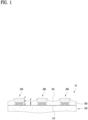
- light emitting elements 200 that configure a multitude of pixels may be located in a manner of being arranged on a wiring substrate 100 equipped with a wiring electrode 110.
- a reflective layer 300 may be located among a multitude of the light emitting elements 200.
- the reflective layer 300 may fill a space between the light emitting elements 200.
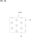
- the reflective layer 300 may include reflective particles 320 (see FIG. 2B ) dispersed in a transparent resin layer 310 (see FIG. 2B ). This will be described in detail later.
- the wiring electrode 110 is schematically illustrated. A multitude of the wiring electrodes 110 may be located on a wiring substrate 100 in a manner of being partitioned.
- the wiring electrode 110 may include a data electrode (i.e., a pixel electrode) and a scan electrode (i.e., a common electrode).
- the wiring electrode 110 arranged on the wiring substrate 100 may be connected to a TFT layer provided with a Thin Film Transistor (TFT).
- TFT Thin Film Transistor
- the data electrode i.e., the pixel electrode
- TFT layer may be connected to such a TFT layer. A detailed description thereof will be omitted.
- the reflective layer 300 may have a hang structure 301 between the neighboring light emitting elements 200. That is, a curved structure 301 formed concavely between the neighboring light emitting elements 200 and continuously connected may be formed on a top surface of the reflective layer 300.
- a maximum height a of the light emitting element 200 may be different from a minimum height a' of the reflective layer 300.
- the minimum height a' of the reflective layer 300 may be lower than the maximum height a of the light emitting element 200.
- the height a' of the hang structure 301 may be higher than half of the height a of the light emitting element 200.
- the hang structure 301 may be associated with a fabricating process of the reflective layer 300. For example, when the reflective layer 300 is formed using a jetting process in which material is applied using a nozzle and then cured, the hang structure 301 may be formed.
- the light emitting element 200 may be disposed on the wiring substrate 100 in a manner of forming an individual pixel.
- a single light emitting element 200 may be configured to form a single pixel. Since the reflective layer 300 is formed to surround at least the side of the single light emitting element 200 forming the individual pixel, light emitted from the light emitting element 200 may be emitted upward without being mixed with light emitted from another light emitting element 200 forming a neighboring pixel.
- the light emitting element 200 forming the individual pixel may include a semiconductor structure including a multitude of semiconductor layers 210, 220, and 230 stacked to emit light of a first color, a second color, and a third color.
- such a layered light emitting device 200 may include a semiconductor structure including a first semiconductor layer 210 emitting red light, a second semiconductor layer 220 emitting blue light, and a third semiconductor layer 230 emitting green light.
- each of the first semiconductor layer 210, the second semiconductor layer 220, and the third semiconductor layer 230 may include semiconductor layers capable of emitting light of individual colors.
- each of the first semiconductor layer 210, the second semiconductor layer 220, and the third semiconductor layer 230 may include an active layer capable of emitting light of each individual color.
- each of the first semiconductor layer 210, the second semiconductor layer 220, and the third semiconductor layer 230 may include an n-type semiconductor layer and a p-type semiconductor layer together with an active layer capable of emitting light of an individual color. This individual structure is omitted in FIG. 2A .
- the light emitting element 200 may include a first electrode 250 and a second electrode 260 electrically connected to one side and the other side of the semiconductor structure, respectively.
- the semiconductor structure and the electrical connection structure of the first electrode 250 and the second electrode 260 are schematically illustrated.
- extension pads 251 and 261 may be provided to the first electrode 250 and the second electrode 260 electrically connected to one side and the other side of the semiconductor structure, respectively.
- the sizes of the extension pads 251 and 261 may increase to be larger than the outer surface of the semiconductor structure.
- the reflective layer 300 may be located to surround lateral sides of the semiconductor structure including the first semiconductor layer 210, the second semiconductor layer 220, and the third semiconductor layer 230 of the light emitting element 200 at least.
- the reflective layer 300 may be located to cover the first electrode 250 and the second electrode 260. In addition, for example, the reflective layer 300 may be located to cover the extension pads 251 and 261.
- the reflective layer 300 may be located to further surround a lateral side of the support layer 240 of the light emitting element 200. In an example not belonging to the present invention, the reflective layer 300 may be located to surround all sides except the top side of the support layer 240 of the light emitting element.
- the reflective layer 300 includes reflective particles 320 dispersed in the transparent resin layer 310.
- the refractive index of the reflective particles 320 may be different from the refractive index of the transparent resin layer 310.
- the reflective particles 320 may include at least one of silicon, titanium, zirconium, or an oxide thereof, that is, silicon oxide (SiOx), titanium oxide (Ti-Ox), and zirconium oxide (ZrOx).
- the transparent resin layer 310 may be formed of a resin material.
- the transparent resin layer 310 may include at least one material of silicon, epoxy, and urethane.
- the thickness of the reflective layer 300 may be set to have a reflectivity of 90% or more by the transparent resin layer 310 and the reflective particles 320.
- FIG. 3 is a cross-sectional diagram showing a light emitting element of a display device using light emitting elements.
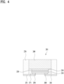
- FIG. 4 is a diagram showing a modified example of the light emitting element of FIG. 3 .
- a light emitting element 201 forming an individual pixel may include a semiconductor structure including a multitude of semiconductor layers 210, 220, and 230 stacked to emit lights of a first color, a second color, and a third color, respectively.
- the light emitting element 201 may include a layered semiconductor light emitting element capable of emitting red, green, and blue lights.
- the layered light emitting element 201 may include a semiconductor structure including a first semiconductor layer 210 emitting red light, a second semiconductor layer 220 emitting blue light, and a third semiconductor layer 230 emitting green light.
- each of the first semiconductor layer 210, the second semiconductor layer 220, and the third semiconductor layer 230 may include a semiconductor layer capable of emitting light of an individual color.
- each of the first semiconductor layer 210, the second semiconductor layer 220, and the third semiconductor layer 230 may include an active layer capable of emitting light of each individual color.
- each of the first semiconductor layer 210, the second semiconductor layer 220, and the third semiconductor layer 230 may include an n-type semiconductor layer and a p-type semiconductor layer together with an active layer capable of emitting light of each individual color.
- the light emitting element 201 may include a first electrode 250 and a second electrode 260 electrically connected to one side and the other side of the semiconductor structure, respectively.
- a support layer 240 may be located on the semiconductor structure.
- the support layer 240 may include a growth substrate in which a semiconductor structure is grown or a transfer substrate in which the semiconductor structure is transferred and bonded.
- the size of the support layer 240 in a plane direction may be larger than that of the semiconductor structure.
- Reflective layers 270 and 271 may be located on a lateral side of the semiconductor structure of the light emitting element 201.
- the reflective layers 270 and 271 may be located to surround the lateral side of the semiconductor structure including the first semiconductor layer 210, the second semiconductor layer 220, and the third semiconductor layer 230 at least.
- the reflective layers 270 and 271 may be located to cover the first electrode 250 and the second electrode 260.
- the reflective layers 270 and 271 may be located to further surround the lateral side of the support layer 240 of the light emitting element 201.
- the reflective layer 300 may be located to surround all sides except the top side of the support layer 240 of the light emitting element.
- the reflective layer may include a first reflective layer 271 covering the lateral side and the bottom side of the semiconductor structure including the first semiconductor layer 210, the second semiconductor layer 220, and the third semiconductor layer 230 and the lateral sides of the first and second electrodes 250 and 260 and a second reflective layer 270 covering the lateral sides of the first reflective layer 271 and the support layer 240.
- the reflective layers 270 and 271 may substantially extend the size of the light emitting element 201.
- the light emitting surface of the light emitting element 201 may be extended to a size including the reflective layers 270 and 271. That is, the light emitting surface having an area corresponding to the semiconductor structure may be extended to the size including the reflective layers 270 and 271.
- extension pads 251 and 261 respectively connected to the first electrode 250 and the second electrode 260 may be further provided.
- the sizes of the extension pads 251 and 261 may be increased to be larger than the outer surface of the semiconductor structure.
- the sizes of the extension pads 251 and 261 may extend to the outer surface of the reflective layer 270.
- the top sides of the extension pads 251 and 261 may be in contact with the reflective layers 270 and 271.
- the extension pads 251 and 261 may further improve the reflectivity of the reflective layers 270 and 271.
- the extension pads 251 and 261 may form substantially external electrode pads of the light emitting element 201.
- the reflective layers 270 and 271 may include reflective particles 320 dispersed in a transparent resin layer 310. That is, properties of the reflective layers 270 and 271 of the present embodiment may be substantially the same as those of the reflective layer 300 described above. In other words, the properties of the reflective layers 270 and 271 of the present embodiment may be the same as those of the reflective layer 300 described above, except for the property of having the hang structure 301. Thus, redundant descriptions will be omitted.
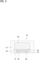
- FIG. 5 is a cross-sectional diagram showing a light emitting element of a display device using light emitting elements according to an embodiment of the present invention.
- FIG. 6 is a diagram showing a modified example of the light emitting element of FIG. 5 .
- a light emitting device 201 forming an individual pixel includes a semiconductor structure including a multitude of semiconductor layers 210, 220, and 230 stacked to emit lights of a first color, a second color, and a third color, respectively. Since the description of the semiconductor structure is the same as the description described with reference to FIG. 3 , a redundant description will be omitted.
- the light emitting element 201 includes a first electrode 250 and a second electrode 260 electrically connected to one side and the other side of the semiconductor structure, respectively.
- a support layer 240 is located on the semiconductor structure.
- the support layer 240 may include a growth substrate in which a semiconductor structure is grown or a transfer substrate in which the semiconductor structure is transferred and bonded.
- the size of the support layer 240 in a plane direction may be larger than that of the semiconductor structure.
- Reflective layers 271 and 272 are located on a lateral side of the semiconductor structure of the light emitting element 201.
- the reflective layer includes a first reflective layer 271 covering lateral and bottom sides of the semiconductor structure including a first semiconductor layer 210, a second semiconductor layer 220, and a third semiconductor layer 230 and lateral sides of the first and second electrodes 250 and 260 and a second reflective layer 272 covering the first reflective layer 271 and lateral and top sides of the support layer 240.
- the second reflective layer 272 is located to surround the lateral and top sides of the support layer 240 of the light emitting element 201.
- the second reflective layer 272 may improve uniformity of light emitted from the light emitting element 201.
- the reflective layers 271 and 272 may substantially extend the size of the light emitting element 201.
- a light emitting surface of the light emitting element 201 may be extended to a size including the reflective layers 271 and 272. That is, the light emitting surface having an area corresponding to the semiconductor structure may be extended to the size including the reflective layers 271 and 272.
- extension pads 251 and 261 respectively connected to the first electrode 250 and the second electrode 260 may be further provided.
- the sizes of the extension pads 251 and 261 may increase to be larger than the outer surface of the semiconductor structure.
- the sizes of the extension pads 251 and 261 may extend to the outer surface of the reflective layer 272.
- top sides of the extension pads 251 and 261 may be in contact with the reflective layers 271 and 272.
- the extension pads 251 and 261 may further improve the reflectivity of the reflective layers 271 and 272.
- the extension pads 251 and 261 may form substantially external electrode pads of the light emitting element 201.
- the reflective layers 271 and 272 include reflective particles 320 dispersed in a transparent resin layer 310. That is, properties of the reflective layers 271 and 272 of the present embodiment are substantially the same as those of the reflective layer 300 described above. In other words, except for the property of having the hang structure 301, the properties of the reflective layers 271 and 272 of the present embodiment may be the same as those of the reflective layer 300 described above. Thus, redundant descriptions will be omitted.
- FIG. 7 is a cross-sectional diagram showing a light emitting element of a display device using light emitting elements according to another embodiment of the present invention.
- FIG. 7 an embodiment of a display device 10 in which the light emitting element 201 according to the embodiment of FIG. 4 forms an individual pixel is illustrated.
- the light emitting element 201 is installed on a wiring substrate 100 to form an individual pixel.
- a gap layer 400 may fill a space between the individual light emitting elements 201.
- the display device 10 may be implemented with a simple structure by using the light emitting element 201 having a structure extended by the reflective layers 270, 271, and 272.
- a module display device 10 including a predetermined number of light emitting elements 201 may be implemented on the wiring substrate 100 having a predetermined size.
- the display device 10 having a desired size may be fabricated by combining the module display devices 10.
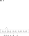
- FIGs. 8 to 11 are schematic cross-sectional diagrams showing a process for fabricating a light emitting element of a display device using light emitting elements according to an example not belonging to the present invention.
- FIGs. 8 to 11 a process of fabricating a light emitting element according to the embodiment shown in FIG. 4 are shown step by step.
- a support layer 240 may be located on a first substrate 500 to form a predetermined gap G.
- a semiconductor structure located on the support layer 240 is omitted.
- a photoresist 600 may be formed on the first electrode 250 and the second electrode 260.
- a reflective layer 273 may be entirely formed in the state shown in FIG. 8 .
- the reflective layer 273 may have the same properties as the reflective layers 300, 270, 271, and 272 described above.
- the thickness of a top side of the structure shown FIG. 9 may be reduced.
- a photoresist 601 having a thinned thickness may be located on the first electrode 250 and the second electrode 260.
- a reflective layer 274 having a thinned thickness may be located among the support layer 240, the first electrode 250, and the second electrode 260. That is, the reflective layer 274 may be located between the structures that will form the respective light emitting elements.
- a metal to form an extension pad 252 may be formed in a state in which the photoresist 601 is removed.
- the light emitting element 201 having the structure shown in FIG. 4 may be fabricated.
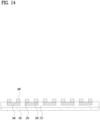
- FIGs. 12 to 15 are schematic cross-sectional diagrams showing a process for fabricating a light emitting element of a display device using light emitting elements according to one embodiment of the present invention.
- FIGs. 12 to 15 a process of fabricating a light emitting element shown in FIG. 6 is shown step by step.
- a reflective layer 273 may be entirely formed in the state shown in FIG. 11 .
- the reflective layer 273 may have the same properties as the reflective layers 300, 270, 271, and 272 described above.
- the structure formed in FIG. 13 may be transferred to a second substrate 501.
- a photoresist 600 may be formed on the first electrode 250 and the second electrode 260.
- a reflective layer 273 may be located between the second substrate 501 and the support layer 240.
- a metal to form an extension pad 252 may be formed in a state in which the photoresist 600 is removed.
- a light emitting element 201 having the structure shown in FIG. 6 may be fabricated.
- FIG. 16 is a diagram of pictures showing light emitting states by a light emitting element of a display device using light emitting elements according to another embodiment of the present disclosure.
- FIG. 16 (a) illustrates a light emitting state by a light emitting element in a state in which the reflective layers 270, 271, and 272 are not provided as a comparative example.
- FIG. 16 (b) illustrates a light emitting state by the light emitting element in a state in which the reflective layers 270, 271, and 272 are provided as an embodiment.
- the size of the light emitting element 201 may be substantially extended by the reflective layers 270, 271, and 272. That is, the light emitting surface having an area corresponding to the semiconductor structure may be extended to a size including the reflective layers 270, 271, and 272.
- light traveling to a lateral side of a light emitting element is made to travel to a front side, thereby increasing light efficiency.
Landscapes
- Devices For Indicating Variable Information By Combining Individual Elements (AREA)
Claims (10)
- Anzeigevorrichtung (10), umfassend:ein Verdrahtungssubstrat (100);eine Mehrzahl von lichtemittierenden Elementen (201), wobei jedes lichtemittierende Element (201) der Mehrzahl von lichtemittierenden Elementen (201) auf dem Verdrahtungssubstrat (100) angeordnet ist, um ein einzelnes Pixel zu bilden, und eine Halbleiterstruktur aufweist, die eine Mehrzahl von Halbleiterschichten (210, 220, 230), die gestapelt sind, um Licht einer jeweiligen ersten bis dritten Farbe zu emittieren, eine erste und eine zweite Elektrode (250, 260), die elektrisch mit einer Seite und einer anderen Seite der Halbleiterstruktur auf einer ersten Fläche der Halbleiterstruktur verbunden sind, und eine Trägerschicht (240), die auf einer zweiten Fläche der Halbleiterstruktur angeordnet ist, enthält; undeine reflektierende Schicht, die einen Raum zwischen der Mehrzahl von lichtemittierenden Elementen (201) ausfüllt, wobei die reflektierende Schicht umfasst:eine transparente Harzschicht (310); undreflektierende Partikel (320), die in der transparenten Harzschicht (310) verteilt sind,wobei die reflektierende Schicht eine erste Reflexionsschicht (271), die die laterale Seite und eine untere Seite der Halbleiterstruktur jedes lichtemittierenden Elements (201) bedeckt, und eine zweite Reflexionsschicht (272), die die lateralen Seiten der ersten Reflexionsschicht (271) und die Trägerschicht (240) jedes lichtemittierenden Elements (201) bedeckt und auf einer oberen Seite der Trägerschicht (240) jedes lichtemittierenden Elements (201) angeordnet ist, umfasst.
- Anzeigevorrichtung (10) nach Anspruch 1, wobei die reflektierende Schicht eine Hängestruktur (301) zwischen benachbarten lichtemittierenden Elementen (201) aufweist.
- Anzeigevorrichtung (10) nach Anspruch 2, wobei eine Höhe der Hängestruktur (301) größer ist als die Hälfte der Höhe jedes der benachbarten lichtemittierenden Elemente (201).
- Anzeigevorrichtung (10) nach einem der Ansprüche 1 bis 3, wobei sich der Brechungsindex der reflektierenden Partikel (320) von einem Brechungsindex der transparenten Harzschicht (310) unterscheidet.
- Anzeigevorrichtung (10) nach einem der Ansprüche 1 bis 4, wobei die reflektierenden Partikel (320) mindestens eines von Siliziumoxid, Titanoxid oder Zirkoniumoxid enthalten.
- Anzeigevorrichtung (10) nach einem der Ansprüche 1 bis 5, wobei die Dicke der reflektierenden Schicht so eingestellt ist, dass sie durch die transparente Harzschicht (310) und die reflektierenden Partikel (320) ein Reflexionsvermögen von 90 % oder mehr aufweist.
- Anzeigevorrichtung (10) nach einem der Ansprüche 1 bis 6, wobei die transparente Harzschicht (310) mindestens ein Material aus Silikon, Epoxid oder Urethan enthält.
- Anzeigevorrichtung (10) nach Anspruch 1, wobei die erste Reflexionsschicht (271) eine vorbestimmte Dicke auf der lateralen Seite der Halbleiterstruktur aufweist.
- Anzeigevorrichtung (10) nach Anspruch 1, wobei jedes lichtemittierende Element (201) ferner ein Verlängerungskissen (251, 261) umfasst, das mit jeder der ersten Elektrode (250) und der zweiten Elektrode (260) verbunden ist.
- Anzeigevorrichtung (10) nach Anspruch 9, wobei ein äußeres Seitenende des Verlängerungskissens (251, 261) in Kontakt mit der reflektierenden Schicht ist.
Applications Claiming Priority (3)
| Application Number | Priority Date | Filing Date | Title |
|---|---|---|---|
| KR20210171554 | 2021-12-03 | ||
| KR20210179325 | 2021-12-15 | ||
| KR1020220126612A KR102898783B1 (ko) | 2021-12-03 | 2022-10-04 | 적층형 발광 소자 및 이를 이용한 디스플레이 장치 |
Publications (2)
| Publication Number | Publication Date |
|---|---|
| EP4191667A1 EP4191667A1 (de) | 2023-06-07 |
| EP4191667B1 true EP4191667B1 (de) | 2025-04-23 |
Family
ID=84387686
Family Applications (1)
| Application Number | Title | Priority Date | Filing Date |
|---|---|---|---|
| EP22211129.6A Active EP4191667B1 (de) | 2021-12-03 | 2022-12-02 | Anzeigevorrichtung |
Country Status (2)
| Country | Link |
|---|---|
| US (1) | US20230178694A1 (de) |
| EP (1) | EP4191667B1 (de) |
Citations (2)
| Publication number | Priority date | Publication date | Assignee | Title |
|---|---|---|---|---|
| US20140191272A1 (en) * | 2011-07-19 | 2014-07-10 | Osram Opto Semiconductors Gmbh | Optoelectronic Component and Method for Producing an Optoelectronic Component |
| US20210184083A1 (en) * | 2019-12-12 | 2021-06-17 | Lumileds Llc | Light emitting diodes with reflective sidewalls comprising porous particles |
Family Cites Families (7)
| Publication number | Priority date | Publication date | Assignee | Title |
|---|---|---|---|---|
| CN104559456A (zh) * | 2014-12-25 | 2015-04-29 | 无锡德贝尔光电材料有限公司 | Led用白色阻焊油墨 |
| KR101771461B1 (ko) * | 2015-04-24 | 2017-08-25 | 엘지전자 주식회사 | 반도체 발광 소자를 이용한 디스플레이 장치 및 이의 제조방법 |
| KR102415331B1 (ko) * | 2015-08-26 | 2022-06-30 | 삼성전자주식회사 | 발광 소자 패키지, 및 이를 포함하는 장치 |
| US10892296B2 (en) * | 2017-11-27 | 2021-01-12 | Seoul Viosys Co., Ltd. | Light emitting device having commonly connected LED sub-units |
| JP7082279B2 (ja) * | 2018-03-29 | 2022-06-08 | 日亜化学工業株式会社 | 発光装置およびその製造方法 |
| KR102694329B1 (ko) * | 2018-12-10 | 2024-08-13 | 삼성전자주식회사 | 디스플레이 모듈, 이를 포함하는 디스플레이 장치 및 디스플레이 모듈 제조 방법 |
| US11527614B2 (en) | 2021-03-09 | 2022-12-13 | Taiwan Semiconductor Manufacturing Company, Ltd. | Semiconductor structure with conductive structure and method for manufacturing the same |
-
2022
- 2022-12-02 EP EP22211129.6A patent/EP4191667B1/de active Active
- 2022-12-02 US US18/061,318 patent/US20230178694A1/en active Pending
Patent Citations (2)
| Publication number | Priority date | Publication date | Assignee | Title |
|---|---|---|---|---|
| US20140191272A1 (en) * | 2011-07-19 | 2014-07-10 | Osram Opto Semiconductors Gmbh | Optoelectronic Component and Method for Producing an Optoelectronic Component |
| US20210184083A1 (en) * | 2019-12-12 | 2021-06-17 | Lumileds Llc | Light emitting diodes with reflective sidewalls comprising porous particles |
Also Published As
| Publication number | Publication date |
|---|---|
| US20230178694A1 (en) | 2023-06-08 |
| EP4191667A1 (de) | 2023-06-07 |
Similar Documents
| Publication | Publication Date | Title |
|---|---|---|
| US11251225B2 (en) | Light emitting diode module, display panel having the same and method of manufacturing the same | |
| US10797040B2 (en) | Method of manufacturing display module using LED | |
| KR102689439B1 (ko) | 표시 장치 및 그의 제조 방법 | |
| KR102941804B1 (ko) | 마이크로 led를 이용한 디스플레이 장치 | |
| US11650457B2 (en) | Demarcating member, demarcating structure body, surface light source, and liquid-crystal display device | |
| US11984469B2 (en) | Display device | |
| KR20200024732A (ko) | 표시장치 | |
| US20240312967A1 (en) | Display panel | |
| KR102898783B1 (ko) | 적층형 발광 소자 및 이를 이용한 디스플레이 장치 | |
| US12376440B2 (en) | Mother substrate for display panel, display panel using the same | |
| US20240379922A1 (en) | Light-emitting element package, display device using the same, and method for manufacturing display device | |
| EP4191667A1 (de) | Geschichtetes lichtemittierendes element und anzeigevorrichtung damit | |
| KR20200005096A (ko) | 반도체 발광 소자를 이용한 디스플레이 장치 및 이의 제조방법 | |
| KR20230102354A (ko) | 표시 장치 | |
| JP2023179115A (ja) | 表示装置 | |
| WO2024020805A1 (zh) | 背光模组及显示装置 | |
| US20260033084A1 (en) | Display apparatus | |
| KR102917219B1 (ko) | 발광 소자 패키지 및 이를 이용한 디스플레이 장치 | |
| US20260033095A1 (en) | Display device | |
| KR102896303B1 (ko) | 표시장치 | |
| US20250366292A1 (en) | Display panel | |
| US20250070097A1 (en) | Display device using semiconductor light emitting diodes | |
| US20250185372A1 (en) | Display device | |
| KR20260014422A (ko) | 표시 장치 | |
| KR20260033668A (ko) | 표시 장치 |
Legal Events
| Date | Code | Title | Description |
|---|---|---|---|
| PUAI | Public reference made under article 153(3) epc to a published international application that has entered the european phase |
Free format text: ORIGINAL CODE: 0009012 |
|
| STAA | Information on the status of an ep patent application or granted ep patent |
Free format text: STATUS: REQUEST FOR EXAMINATION WAS MADE |
|
| 17P | Request for examination filed |
Effective date: 20221202 |
|
| AK | Designated contracting states |
Kind code of ref document: A1 Designated state(s): AL AT BE BG CH CY CZ DE DK EE ES FI FR GB GR HR HU IE IS IT LI LT LU LV MC ME MK MT NL NO PL PT RO RS SE SI SK SM TR |
|
| STAA | Information on the status of an ep patent application or granted ep patent |
Free format text: STATUS: EXAMINATION IS IN PROGRESS |
|
| 17Q | First examination report despatched |
Effective date: 20240320 |
|
| GRAP | Despatch of communication of intention to grant a patent |
Free format text: ORIGINAL CODE: EPIDOSNIGR1 |
|
| STAA | Information on the status of an ep patent application or granted ep patent |
Free format text: STATUS: GRANT OF PATENT IS INTENDED |
|
| INTG | Intention to grant announced |
Effective date: 20241119 |
|
| RAP3 | Party data changed (applicant data changed or rights of an application transferred) |
Owner name: LG ELECTRONICS INC. |
|
| GRAS | Grant fee paid |
Free format text: ORIGINAL CODE: EPIDOSNIGR3 |
|
| GRAA | (expected) grant |
Free format text: ORIGINAL CODE: 0009210 |
|
| STAA | Information on the status of an ep patent application or granted ep patent |
Free format text: STATUS: THE PATENT HAS BEEN GRANTED |
|
| AK | Designated contracting states |
Kind code of ref document: B1 Designated state(s): AL AT BE BG CH CY CZ DE DK EE ES FI FR GB GR HR HU IE IS IT LI LT LU LV MC ME MK MT NL NO PL PT RO RS SE SI SK SM TR |
|
| REG | Reference to a national code |
Ref country code: GB Ref legal event code: FG4D |
|
| REG | Reference to a national code |
Ref country code: CH Ref legal event code: EP |
|
| REG | Reference to a national code |
Ref country code: DE Ref legal event code: R096 Ref document number: 602022013498 Country of ref document: DE |
|
| REG | Reference to a national code |
Ref country code: IE Ref legal event code: FG4D |
|
| REG | Reference to a national code |
Ref country code: NL Ref legal event code: MP Effective date: 20250423 |
|
| PG25 | Lapsed in a contracting state [announced via postgrant information from national office to epo] |
Ref country code: NL Free format text: LAPSE BECAUSE OF FAILURE TO SUBMIT A TRANSLATION OF THE DESCRIPTION OR TO PAY THE FEE WITHIN THE PRESCRIBED TIME-LIMIT Effective date: 20250423 |
|
| REG | Reference to a national code |
Ref country code: AT Ref legal event code: MK05 Ref document number: 1788674 Country of ref document: AT Kind code of ref document: T Effective date: 20250423 |
|
| PG25 | Lapsed in a contracting state [announced via postgrant information from national office to epo] |
Ref country code: FI Free format text: LAPSE BECAUSE OF FAILURE TO SUBMIT A TRANSLATION OF THE DESCRIPTION OR TO PAY THE FEE WITHIN THE PRESCRIBED TIME-LIMIT Effective date: 20250423 Ref country code: ES Free format text: LAPSE BECAUSE OF FAILURE TO SUBMIT A TRANSLATION OF THE DESCRIPTION OR TO PAY THE FEE WITHIN THE PRESCRIBED TIME-LIMIT Effective date: 20250423 Ref country code: PT Free format text: LAPSE BECAUSE OF FAILURE TO SUBMIT A TRANSLATION OF THE DESCRIPTION OR TO PAY THE FEE WITHIN THE PRESCRIBED TIME-LIMIT Effective date: 20250825 |
|
| REG | Reference to a national code |
Ref country code: LT Ref legal event code: MG9D |
|
| PG25 | Lapsed in a contracting state [announced via postgrant information from national office to epo] |
Ref country code: NO Free format text: LAPSE BECAUSE OF FAILURE TO SUBMIT A TRANSLATION OF THE DESCRIPTION OR TO PAY THE FEE WITHIN THE PRESCRIBED TIME-LIMIT Effective date: 20250723 Ref country code: GR Free format text: LAPSE BECAUSE OF FAILURE TO SUBMIT A TRANSLATION OF THE DESCRIPTION OR TO PAY THE FEE WITHIN THE PRESCRIBED TIME-LIMIT Effective date: 20250724 |
|
| PG25 | Lapsed in a contracting state [announced via postgrant information from national office to epo] |
Ref country code: PL Free format text: LAPSE BECAUSE OF FAILURE TO SUBMIT A TRANSLATION OF THE DESCRIPTION OR TO PAY THE FEE WITHIN THE PRESCRIBED TIME-LIMIT Effective date: 20250423 |
|
| PG25 | Lapsed in a contracting state [announced via postgrant information from national office to epo] |
Ref country code: BG Free format text: LAPSE BECAUSE OF FAILURE TO SUBMIT A TRANSLATION OF THE DESCRIPTION OR TO PAY THE FEE WITHIN THE PRESCRIBED TIME-LIMIT Effective date: 20250423 |
|
| PG25 | Lapsed in a contracting state [announced via postgrant information from national office to epo] |
Ref country code: HR Free format text: LAPSE BECAUSE OF FAILURE TO SUBMIT A TRANSLATION OF THE DESCRIPTION OR TO PAY THE FEE WITHIN THE PRESCRIBED TIME-LIMIT Effective date: 20250423 |
|
| PG25 | Lapsed in a contracting state [announced via postgrant information from national office to epo] |
Ref country code: AT Free format text: LAPSE BECAUSE OF FAILURE TO SUBMIT A TRANSLATION OF THE DESCRIPTION OR TO PAY THE FEE WITHIN THE PRESCRIBED TIME-LIMIT Effective date: 20250423 |
|
| PG25 | Lapsed in a contracting state [announced via postgrant information from national office to epo] |
Ref country code: RS Free format text: LAPSE BECAUSE OF FAILURE TO SUBMIT A TRANSLATION OF THE DESCRIPTION OR TO PAY THE FEE WITHIN THE PRESCRIBED TIME-LIMIT Effective date: 20250723 |
|
| PG25 | Lapsed in a contracting state [announced via postgrant information from national office to epo] |
Ref country code: IS Free format text: LAPSE BECAUSE OF FAILURE TO SUBMIT A TRANSLATION OF THE DESCRIPTION OR TO PAY THE FEE WITHIN THE PRESCRIBED TIME-LIMIT Effective date: 20250823 |
|
| PG25 | Lapsed in a contracting state [announced via postgrant information from national office to epo] |
Ref country code: LV Free format text: LAPSE BECAUSE OF FAILURE TO SUBMIT A TRANSLATION OF THE DESCRIPTION OR TO PAY THE FEE WITHIN THE PRESCRIBED TIME-LIMIT Effective date: 20250423 |
|
| REG | Reference to a national code |
Ref country code: DE Ref legal event code: R079 Ref document number: 602022013498 Country of ref document: DE Free format text: PREVIOUS MAIN CLASS: H01L0025075000 Ipc: H10H0029240000 |
|
| PGFP | Annual fee paid to national office [announced via postgrant information from national office to epo] |
Ref country code: DE Payment date: 20251105 Year of fee payment: 4 |
|
| PG25 | Lapsed in a contracting state [announced via postgrant information from national office to epo] |
Ref country code: DK Free format text: LAPSE BECAUSE OF FAILURE TO SUBMIT A TRANSLATION OF THE DESCRIPTION OR TO PAY THE FEE WITHIN THE PRESCRIBED TIME-LIMIT Effective date: 20250423 Ref country code: SM Free format text: LAPSE BECAUSE OF FAILURE TO SUBMIT A TRANSLATION OF THE DESCRIPTION OR TO PAY THE FEE WITHIN THE PRESCRIBED TIME-LIMIT Effective date: 20250423 |
|
| PGFP | Annual fee paid to national office [announced via postgrant information from national office to epo] |
Ref country code: FR Payment date: 20251111 Year of fee payment: 4 |
|
| PG25 | Lapsed in a contracting state [announced via postgrant information from national office to epo] |
Ref country code: CZ Free format text: LAPSE BECAUSE OF FAILURE TO SUBMIT A TRANSLATION OF THE DESCRIPTION OR TO PAY THE FEE WITHIN THE PRESCRIBED TIME-LIMIT Effective date: 20250423 |
|
| PG25 | Lapsed in a contracting state [announced via postgrant information from national office to epo] |
Ref country code: EE Free format text: LAPSE BECAUSE OF FAILURE TO SUBMIT A TRANSLATION OF THE DESCRIPTION OR TO PAY THE FEE WITHIN THE PRESCRIBED TIME-LIMIT Effective date: 20250423 |
|
| REG | Reference to a national code |
Ref country code: DE Ref legal event code: R097 Ref document number: 602022013498 Country of ref document: DE |
|
| PG25 | Lapsed in a contracting state [announced via postgrant information from national office to epo] |
Ref country code: SK Free format text: LAPSE BECAUSE OF FAILURE TO SUBMIT A TRANSLATION OF THE DESCRIPTION OR TO PAY THE FEE WITHIN THE PRESCRIBED TIME-LIMIT Effective date: 20250423 |
|
| PG25 | Lapsed in a contracting state [announced via postgrant information from national office to epo] |
Ref country code: IT Free format text: LAPSE BECAUSE OF FAILURE TO SUBMIT A TRANSLATION OF THE DESCRIPTION OR TO PAY THE FEE WITHIN THE PRESCRIBED TIME-LIMIT Effective date: 20250423 |
|
| PLBE | No opposition filed within time limit |
Free format text: ORIGINAL CODE: 0009261 |
|
| STAA | Information on the status of an ep patent application or granted ep patent |
Free format text: STATUS: NO OPPOSITION FILED WITHIN TIME LIMIT |
|
| REG | Reference to a national code |
Ref country code: CH Ref legal event code: L10 Free format text: ST27 STATUS EVENT CODE: U-0-0-L10-L00 (AS PROVIDED BY THE NATIONAL OFFICE) Effective date: 20260304 |
|
| PG25 | Lapsed in a contracting state [announced via postgrant information from national office to epo] |
Ref country code: RO Free format text: LAPSE BECAUSE OF FAILURE TO SUBMIT A TRANSLATION OF THE DESCRIPTION OR TO PAY THE FEE WITHIN THE PRESCRIBED TIME-LIMIT Effective date: 20250423 |
|
| 26N | No opposition filed |
Effective date: 20260126 |