EP4189358B1 - Verfahren zum detektieren von emissionslicht, detektionsvorrichtung und laserscanning-mikroskop - Google Patents
Verfahren zum detektieren von emissionslicht, detektionsvorrichtung und laserscanning-mikroskop Download PDFInfo
- Publication number
- EP4189358B1 EP4189358B1 EP21752522.9A EP21752522A EP4189358B1 EP 4189358 B1 EP4189358 B1 EP 4189358B1 EP 21752522 A EP21752522 A EP 21752522A EP 4189358 B1 EP4189358 B1 EP 4189358B1
- Authority
- EP
- European Patent Office
- Prior art keywords
- pixel
- pixels
- matrix sensor
- spectral
- emission light
- Prior art date
- Legal status (The legal status is an assumption and is not a legal conclusion. Google has not performed a legal analysis and makes no representation as to the accuracy of the status listed.)
- Active
Links
Images


Classifications
-
- G—PHYSICS
- G01—MEASURING; TESTING
- G01J—MEASUREMENT OF INTENSITY, VELOCITY, SPECTRAL CONTENT, POLARISATION, PHASE OR PULSE CHARACTERISTICS OF INFRARED, VISIBLE OR ULTRAVIOLET LIGHT; COLORIMETRY; RADIATION PYROMETRY
- G01J3/00—Spectrometry; Spectrophotometry; Monochromators; Measuring colours
- G01J3/02—Details
- G01J3/027—Control of working procedures of a spectrometer; Failure detection; Bandwidth calculation
-
- G—PHYSICS
- G01—MEASURING; TESTING
- G01J—MEASUREMENT OF INTENSITY, VELOCITY, SPECTRAL CONTENT, POLARISATION, PHASE OR PULSE CHARACTERISTICS OF INFRARED, VISIBLE OR ULTRAVIOLET LIGHT; COLORIMETRY; RADIATION PYROMETRY
- G01J3/00—Spectrometry; Spectrophotometry; Monochromators; Measuring colours
- G01J3/12—Generating the spectrum; Monochromators
- G01J3/18—Generating the spectrum; Monochromators using diffraction elements, e.g. grating
-
- G—PHYSICS
- G01—MEASURING; TESTING
- G01J—MEASUREMENT OF INTENSITY, VELOCITY, SPECTRAL CONTENT, POLARISATION, PHASE OR PULSE CHARACTERISTICS OF INFRARED, VISIBLE OR ULTRAVIOLET LIGHT; COLORIMETRY; RADIATION PYROMETRY
- G01J3/00—Spectrometry; Spectrophotometry; Monochromators; Measuring colours
- G01J3/28—Investigating the spectrum
- G01J3/2823—Imaging spectrometer
-
- G—PHYSICS
- G01—MEASURING; TESTING
- G01N—INVESTIGATING OR ANALYSING MATERIALS BY DETERMINING THEIR CHEMICAL OR PHYSICAL PROPERTIES
- G01N21/00—Investigating or analysing materials by the use of optical means, i.e. using sub-millimetre waves, infrared, visible or ultraviolet light
- G01N21/62—Systems in which the material investigated is excited whereby it emits light or causes a change in wavelength of the incident light
- G01N21/63—Systems in which the material investigated is excited whereby it emits light or causes a change in wavelength of the incident light optically excited
- G01N21/64—Fluorescence; Phosphorescence
- G01N21/645—Specially adapted constructive features of fluorimeters
- G01N21/6456—Spatial resolved fluorescence measurements; Imaging
- G01N21/6458—Fluorescence microscopy
-
- G—PHYSICS
- G02—OPTICS
- G02B—OPTICAL ELEMENTS, SYSTEMS OR APPARATUS
- G02B21/00—Microscopes
- G02B21/0004—Microscopes specially adapted for specific applications
- G02B21/002—Scanning microscopes
- G02B21/0024—Confocal scanning microscopes (CSOMs) or confocal "macroscopes"; Accessories which are not restricted to use with CSOMs, e.g. sample holders
- G02B21/0032—Optical details of illumination, e.g. light-sources, pinholes, beam splitters, slits, fibers
-
- G—PHYSICS
- G02—OPTICS
- G02B—OPTICAL ELEMENTS, SYSTEMS OR APPARATUS
- G02B21/00—Microscopes
- G02B21/0004—Microscopes specially adapted for specific applications
- G02B21/002—Scanning microscopes
- G02B21/0024—Confocal scanning microscopes (CSOMs) or confocal "macroscopes"; Accessories which are not restricted to use with CSOMs, e.g. sample holders
- G02B21/0052—Optical details of the image generation
- G02B21/0076—Optical details of the image generation arrangements using fluorescence or luminescence
-
- G—PHYSICS
- G02—OPTICS
- G02B—OPTICAL ELEMENTS, SYSTEMS OR APPARATUS
- G02B21/00—Microscopes
- G02B21/0004—Microscopes specially adapted for specific applications
- G02B21/002—Scanning microscopes
- G02B21/0024—Confocal scanning microscopes (CSOMs) or confocal "macroscopes"; Accessories which are not restricted to use with CSOMs, e.g. sample holders
- G02B21/008—Details of detection or image processing, including general computer control
-
- G—PHYSICS
- G01—MEASURING; TESTING
- G01J—MEASUREMENT OF INTENSITY, VELOCITY, SPECTRAL CONTENT, POLARISATION, PHASE OR PULSE CHARACTERISTICS OF INFRARED, VISIBLE OR ULTRAVIOLET LIGHT; COLORIMETRY; RADIATION PYROMETRY
- G01J3/00—Spectrometry; Spectrophotometry; Monochromators; Measuring colours
- G01J3/28—Investigating the spectrum
- G01J3/2803—Investigating the spectrum using photoelectric array detector
- G01J2003/2813—2D-array
-
- G—PHYSICS
- G01—MEASURING; TESTING
- G01J—MEASUREMENT OF INTENSITY, VELOCITY, SPECTRAL CONTENT, POLARISATION, PHASE OR PULSE CHARACTERISTICS OF INFRARED, VISIBLE OR ULTRAVIOLET LIGHT; COLORIMETRY; RADIATION PYROMETRY
- G01J3/00—Spectrometry; Spectrophotometry; Monochromators; Measuring colours
- G01J3/28—Investigating the spectrum
- G01J3/44—Raman spectrometry; Scattering spectrometry ; Fluorescence spectrometry
- G01J3/4406—Fluorescence spectrometry
-
- G—PHYSICS
- G01—MEASURING; TESTING
- G01N—INVESTIGATING OR ANALYSING MATERIALS BY DETERMINING THEIR CHEMICAL OR PHYSICAL PROPERTIES
- G01N21/00—Investigating or analysing materials by the use of optical means, i.e. using sub-millimetre waves, infrared, visible or ultraviolet light
- G01N21/62—Systems in which the material investigated is excited whereby it emits light or causes a change in wavelength of the incident light
- G01N21/63—Systems in which the material investigated is excited whereby it emits light or causes a change in wavelength of the incident light optically excited
- G01N21/64—Fluorescence; Phosphorescence
- G01N2021/6417—Spectrofluorimetric devices
- G01N2021/6423—Spectral mapping, video display
-
- G—PHYSICS
- G01—MEASURING; TESTING
- G01N—INVESTIGATING OR ANALYSING MATERIALS BY DETERMINING THEIR CHEMICAL OR PHYSICAL PROPERTIES
- G01N21/00—Investigating or analysing materials by the use of optical means, i.e. using sub-millimetre waves, infrared, visible or ultraviolet light
- G01N21/62—Systems in which the material investigated is excited whereby it emits light or causes a change in wavelength of the incident light
- G01N21/63—Systems in which the material investigated is excited whereby it emits light or causes a change in wavelength of the incident light optically excited
- G01N21/64—Fluorescence; Phosphorescence
- G01N21/6408—Fluorescence; Phosphorescence with measurement of decay time, time resolved fluorescence
Definitions
- a generic detection device for detecting emission light in a laser scanning microscope is also disclosed in [Castello et al. 2019].
- a generic detection device has a two-dimensional matrix sensor in an image plane with a plurality of pixels for spatially oversampling detection of a detection point distribution function of emission light coming from a sample and imaging optics for directing the emission light onto the two-dimensional matrix sensor.
- a generic laser scanning microscope is also described in [Castello et al 2019] and has the following components: a light source, in particular a laser, for emitting excitation light, an excitation beam path with a microscope objective for directing the excitation light onto or into a sample to be examined, a scanning device in the excitation beam path for scanning at least one illumination spot over the sample, a detection beam path for directing emission light emitted by the sample, in particular fluorescent light, to a detection unit, a main color splitter for separating excitation light and emission light, the detection unit for detecting the emission light and a control and evaluation unit, in particular a PC, for controlling the light source and for evaluating measurement data obtained by the detection unit.
- a light source in particular a laser
- an excitation beam path with a microscope objective for directing the excitation light onto or into a sample to be examined
- a scanning device in the excitation beam path for scanning at least one illumination spot over the sample
- a detection beam path for directing emission light emitted by
- SPAD single -photon avalanche diode
- SPAD single -photon avalanche diode
- the pixels can be operated in the so-called Geiger mode, so that photon counting is possible on an area sensor.
- the read-out signal is immediately digital, which enables extremely high frame rates in the range of 1 MHz.
- SPAD cameras also have no readout noise. Readout noise occurs particularly in other sensors such as sCMOS sensors or CCDs and increases significantly with high readout rates.
- EM-CCDs use an amplification mechanism close to the sensor to raise the signal above the readout noise and can therefore in principle be single-photon sensitive.
- amplifier noise also known as excess noise; multiplication noise
- the achievable speeds are fundamentally limited with higher pixel counts.
- sCMOS cameras achieve low readout noise in the range of 0.3e-, which in principle allows photon counting with these cameras.
- US 2020/003551 A1 relates to a method and a device for determining a position of an object with particularly high resolution.
- a detection module that is used to detect fluorophores in axially different planes of a sample.
- Light coming from the sample is split into two sub-channels, each with linear polarization, using a polarization beam splitter, whereby the polarizations of the sub-channels are oriented perpendicular to each other.
- the sub-beams are then converted into circular polarizations and used to generate a conical diffraction pattern through conical crystals.
- One object of the invention can be seen as providing a method of the type specified above which is particularly versatile.
- a suitable detection device and a laser scanning microscope are to be specified.
- the method of the type specified above is further developed according to the invention in that the emission light coming from the sample is spectrally dispersed with a dispersion device, in particular in a dispersion direction, that the spectrally dispersed emission light is detected in a spectrally resolved manner with the matrix sensor and that when evaluating the intensities measured by the pixels of a pixel area, the spectral separation is reduced for at least some of these pixels.
- the detection device of the type specified above is characterized according to the invention further developed in that a dispersion device is present for spectrally separating the emission light, that the matrix sensor is set up and positioned for spectrally resolving detection of the spectrally separated detection light and that evaluation electronics connected to the matrix sensor are present, which are set up to cancel the spectral separation for these pixels when evaluating the intensities measured by the pixels of a pixel area.
- the laser scanning microscope of the type specified above is further developed according to the invention in that the detection unit has a detection device according to the invention.
- a key idea of the invention is that the emission light coming from the sample is spectrally separated so that the spectral components of different fluorescent dyes initially hit different, i.e. spatially separated, areas of the matrix sensor. These areas are identified and each assigned to a fluorescent dye. The spectral separation is then mathematically reduced for at least some of the pixels in the respective areas so that a point distribution function can be determined for the individual fluorescent dyes, in principle as with the known ISM. The respective point distribution functions can therefore be measured for different fluorescent dyes. The spectral separation is expediently carried out for those pixels in which significant intensity is measured.
- a significant advantage of the present invention can be considered to be that both the advantages of spectral flexibility and the effects achieved by oversampling the point spread function in terms of resolution and sensitivity can be achieved.
- the method according to the invention, the detection device according to the invention and the The microscope according to the invention therefore also enables ISM with a spectrally dispersed signal distribution.
- the detection device according to the invention and the microscope according to the invention are characterized in that a particularly high light efficiency and overall stable arrangements can be achieved.
- the detection device according to the invention is particularly suitable for carrying out the method according to the invention.
- detection point distribution function refers to the intensity distribution on the detector that is generated by a point-like luminous object in the sample plane.
- the pixel areas belonging to different dyes can in principle also overlap on the detector. It is important that there is at least a certain spatial separation of the pixel areas. It is clear that the more clearly the pixel areas are separated or the more the spectral signature of the respective dyes differs, the easier and better the evaluation is.
- At least one pixel region is identified based on a spectrum measured with the matrix sensor, which is assigned to the emission of a dye.
- an intensity value associated with a specific wavelength is determined to determine a spectral intensity distribution of the emission light on the matrix sensor by summing the measurement data of a plurality of pixels in a column of the matrix sensor, in particular the measurement data of all pixels in a column of the matrix sensor, perpendicular to the dispersion direction.
- a change in the measurement environment is primarily considered to be a change in the sample to be examined, and possibly also in the location of the sample being examined, which may have been prepared with different dyes.
- samples with spectrally overlapping dyes or fluorescent proteins can also be imaged and measured.
- the pixel areas on the matrix detector overlap and a spectral unmixing of the intensities measured by the individual pixels is carried out.
- Methods for spectral unmixing are known in principle.
- a spectral unmixing procedure before or after removing the spectral splitting. For example, one can first carry out a spectral unmixing procedure for a freely selected number of spectral bands - for two dyes (typically two regions with pure emissions and one region of overlapping emission) - perform the dispersion reduction, then apply image scanning microscopy and then unmix the - in the example three - channels.
- This method can be used to determine the relative proportions of certain spectral components in a pixel. This means that, for example, according to a rule for pixel reassignment (see below), not the entire intensity of a pixel is shifted, but only the weighted portion.
- the arrangement according to the invention can be used to record the corresponding reference spectra.
- spectral unmixing can be carried out line by line and the respective spectral weights can be determined from which the spectrally weighted portions are derived.
- there are also other methods for separating spectral portions such as PCS, SCA, and the use of "deep learning".
- the method according to the invention can be used in particular to determine a detection point distribution function for at least one fluorescent dye.
- a particular advantage of the invention is, however, that it is also possible to determine the detection point distribution function for several dyes with different emission spectra from the measurement data of a measurement.
- the size of the matrix sensor used specifically the number of pixels of this matrix sensor, allows it, a multi-point variant of the method according to the invention is also possible in principle.
- emission light emitted from several points on a sample that are simultaneously illuminated with excitation light is simultaneously directed to the matrix sensor and evaluated.
- the excitation beam path and the detection beam path must be set up for multi-spot excitation and detection.
- the intensity values measured by these pixels are offset against each other, taking into account the spectral intensity distribution of the emission light for the dye belonging to the pixel area and taking into account a spatial intensity distribution of individual spectral components on the matrix sensor.
- the evaluation electronics of the detection device can be set up to offset the intensity values measured by pixels of a pixel area against one another in order to cancel the spectral separation, taking into account a spectral intensity distribution of the emission light for the dye belonging to the pixel area and taking into account a spatial intensity distribution of individual spectral components on the matrix sensor.
- the spatial intensity distribution of the individual spectral components determines how strongly the spectral components of a point distribution function of a dye, which are shifted relative to each other on the matrix sensor, spatially overlap in the dispersion direction.
- An intensity distribution that is measured from pixels in a column perpendicular to the dispersion direction, in particular from the column in which the highest intensities are measured in the respective pixel area, can be used as the spatial intensity distribution of the individual spectral components.
- the assumption behind this is that the detection point distribution function on the matrix sensor is rotationally symmetrical, i.e. circular. If rotationally symmetrical optics are used, this is a good assumption.
- the withdrawal of the spectral separation for the individual pixels of a pixel area is accomplished by pixel reassignment.
- image scanning microscopy ISM
- the evaluation electronics of the detection device are designed to assign the intensity values measured by the pixels to a location in the image plane that is shifted relative to the respective pixel (pixel reassignment) in order to cancel the spectral separation for the individual pixels of a pixel area, wherein the shift vector depends on the location of the respective pixel and on the wavelength associated with this location.
- the intensity values measured by the pixels are assigned to a location in the image plane that is shifted relative to the respective pixel (pixel reassignment).
- pixel reassignment a shift vector depends on the location of the respective pixel, but here also on the wavelength associated with this location.
- a shift vector is determined for each pixel that depends on the location of the pixel in question and the wavelength associated with the pixel in question.
- the intensity value measured for the pixel in question is then assigned to a location that is shifted relative to the pixel in question by the shift vector.
- a wavelength-independent part of the displacement vector for a particular pixel can be obtained by scaling a vector component of a vector from a reference pixel to the pixel in question with a reassignment factor.
- a reassignment factor of -1/2, i.e. the intensity values measured from a particular pixel would be assigned to a location in the image plane that is just in the middle of the distance from a reference pixel to the pixel in question.
- the pixel reassignment is carried out in such a way that a detection point distribution function obtained in the dispersion direction has essentially the same shape as perpendicular to the dispersion direction.
- the assumption behind this is that the detection point distribution function must have a circularly symmetric intensity distribution when using rotationally symmetric optics.
- the displacement vectors belonging to a wavelength range associated with a sample structure can be determined by evaluating a phase correlation of a plurality of scanned images.
- Analog integrating and/or photon counting detectors can be used as matrix sensors in the detection device according to the invention.
- an sCMOS camera, an EMCCD camera and/or a charge integrating sensor are used.
- the matrix sensor has a SPAD camera or a SPAD camera is used as the matrix sensor.
- the matrix sensor, in particular the SPAD camera is operated in a photon counting mode in which individual photons can be counted. This mode, which is also referred to as "Geiger mode", is characterized by a particularly favorable signal-to-noise ratio.
- light-diffractive and/or light-refracting devices can be used as the dispersion device.
- the dispersion device particularly preferably has a grating, in particular a line grating, and/or a prism.
- a grism i.e. a combination a prism and a grating.
- the dispersion direction lies in the direction and in particular parallel to a coordinate direction of the matrix sensor.
- the pixels in the direction of the dispersion direction can be referred to as pixel rows and the pixels in the direction perpendicular to the dispersion direction can be referred to as pixel columns.
- the alignment of the matrix sensor in such a way that the dispersion direction is parallel to the direction of the pixel rows has the advantage that the pixels in the pixel columns each belong to exactly the same wavelength range or, to put it simply, to exactly the same wavelength.
- a pixel pitch (in principle the lattice constant) of the matrix sensor is selected to be larger than a change in the width of an Airy disk of the detection point distribution function in the plane of the matrix sensor over a spectral bandwidth of a dye.
- the matrix sensor and/or the optical imaging onto the matrix sensor are dimensioned such that a spectral bandwidth per pixel of the matrix sensor in the dispersion direction is less than 0.5 nm, preferably less than 0.4 nm, particularly preferably less than 0.3 nm.
- these embodiments enable an assumption that simplifies the calculation. More precisely, one can then assume, to a good approximation, that the width of the Airy disk over the course of the spectrum of a dye essentially does not depend on the wavelength. Nevertheless, sufficient spectral resolution is achieved.
- the matrix sensor and/or the optical image on the matrix sensor can further be dimensioned such that a diameter of an Airy disk of the detection point distribution function in the plane of the matrix sensor is smaller than twenty times the lattice constant, particularly preferably smaller than seven times the lattice constant and particularly preferably smaller than five times the lattice constant of the matrix sensor.
- the calculation of the discrete unfolding can advantageously be limited to comparatively few wavelengths, namely to the number that corresponds to the number of pixels covered by the respective Airy disk.
- the diameter of the Airy disk on the matrix sensor can be larger than three times the lattice constant, so that finally a process can be carried out which in its last stage is equivalent to an ISM.
- the present invention also enables spectral resolution. This combination is particularly attractive.
- time-resolved measurements for determining fluorescence lifetimes of the dyes are carried out with the matrix sensor, for example with some pixels of the matrix sensor and in particular with each individual pixel of the matrix sensor.
- the matrix sensor and the electronics should therefore be designed for this application in such a way that a time-resolved measurement is possible with each pixel, so that the fluorescence lifetime can be determined.
- These variants of the present invention therefore enable the combination of spectrally resolved FLIM with image scanning. Pulsed lasers are expediently used for these measurements.
- the microscope according to the invention can have means for blocking out excitation light, in particular at least one emission filter.
- a changing device for example a filter wheel, with a plurality of emission filters can be present.
- the detection device according to the invention also enables process variants in which spectrally undesirable components of the emission light are not evaluated.
- the corresponding pixels, in particular pixel columns, of the matrix sensor can be set passively or inactively.
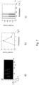
- FIG. 2a shows a schematic representation of an embodiment of a detection device 200 according to the invention.
- the detection device 200 for the spectrally resolved detection of emission light 28 in a laser scanning microscope 100 has the following essential components: a dispersion device 40 for the spectral separation of emission light 28 which comes from the sample S under investigation, a two-dimensional matrix sensor 50 for the spatially resolved detection of the spectrally decomposed emission light and an imaging optics 48 for directing the spectrally decomposed emission light to the two-dimensional matrix sensor 50.
- the imaging optics 48 focus the different spectral components 42, 44, 46, 47 on the matrix sensor 50 with a plurality of pixels 51.
- the matrix sensor 50 can be, for example, a SPAD multi-line camera with, for example, 5 lines with 800 pixels each, corresponding to 800 columns.
- Figure 2b shows a schematic representation of the area of the matrix sensor 50.
- the matrix sensor 50 is positioned relative to the grating 43 so that the dispersion direction 41 is in the direction of the lines, i.e. parallel to the x-direction of the Figure 2b ) shown in the coordinate system.
- the direction of the columns is parallel to the y-direction.
- the blue spectral components are located at the left edge of the spectrum and the red spectral components are located at the right edge of the spectrum.
- the indices i and j designate the columns and rows of the matrix sensor 50, ie the pixel (i, j) is the pixel in the i-th column in the j-th row.
- the imaging optics 48 are first dimensioned relative to the dimensions of the matrix sensor 50, in the example shown, the dimensions of the SPAD camera.
- the various spectral components must be numerically integrated in order to recover the point spread function from the dispersively smeared signal distribution. Once the intensities of the pixels have been obtained in this way, the next step is to use the method of image scanning microscopy (ISM).
- ISM image scanning microscopy
- the last remaining integral can also be ⁇ ⁇ x i Airy(x - x 0 ( ⁇ n ))dx.
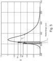
- Figure 7b shows the sum of the signals along the image lines (in x-direction) of the SPAD camera 50, which represents the point distribution function.
- Figure 7c) shows the sum of the counts of all pixels in a column, i.e. in y-direction, and is identical to the detected spectrum of the dye.
- each pixel (i, j) of the matrix sensor delivers a shifted image.
- the images can also simply be registered on top of each other or other forms of calculation, such as multi-view unfolding, can be used to advantageously calculate signals from all pixels.
- a measurement can be carried out, for example, in such a way that the spectral components of a specific emission band, which correspond to a pixel area on the matrix sensor 50, are spectrally combined in such a way that the method of so-called image scanning (also referred to as airy scanning or optical reassignment)
- image scanning also referred to as airy scanning or optical reassignment
- the pixel (12, 3) represents the reference pixel with the associated reference wavelength ⁇ r , to which the signals of the other pixels are related.
- “Shifting back” here means assigning the signals of the respective pixels to numerically specific locations in the plane of the matrix sensor and thus in the sample plane. In contrast to the known methods, however, the shift here must be carried out in such a way that the dispersion is correctly taken into account.
- the proportionality constant ⁇ has the unit of a length and is determined by the strength of the dispersion of the dispersive element, in particular by the lattice constant of the grating used 43.
- n ( n x , n y ) .
- FFT and FFT -1 mean the (Fast) Fourier Transformation or its inverse in a generally known way.
- the maximum of this correlation s i , j x s i , j y arg Max n x n y r i , j n then provides the respective displacement vector by which the image content must be shifted back.
Landscapes
- Physics & Mathematics (AREA)
- General Physics & Mathematics (AREA)
- Chemical & Material Sciences (AREA)
- Analytical Chemistry (AREA)
- Spectroscopy & Molecular Physics (AREA)
- Optics & Photonics (AREA)
- Health & Medical Sciences (AREA)
- Life Sciences & Earth Sciences (AREA)
- Nuclear Medicine, Radiotherapy & Molecular Imaging (AREA)
- Biochemistry (AREA)
- General Health & Medical Sciences (AREA)
- Immunology (AREA)
- Pathology (AREA)
- Engineering & Computer Science (AREA)
- Computer Vision & Pattern Recognition (AREA)
- General Engineering & Computer Science (AREA)
- Investigating, Analyzing Materials By Fluorescence Or Luminescence (AREA)
- Microscoopes, Condenser (AREA)
Applications Claiming Priority (2)
| Application Number | Priority Date | Filing Date | Title |
|---|---|---|---|
| DE102020120190.7A DE102020120190A1 (de) | 2020-07-30 | 2020-07-30 | Verfahren zum detektieren von emissionslicht, detektionsvorrichtung und laser-scanning-mikroskop |
| PCT/EP2021/071269 WO2022023474A1 (de) | 2020-07-30 | 2021-07-29 | Verfahren zum detektieren von emissionslicht, detektionsvorrichtung und laserscanning-mikroskop |
Publications (2)
| Publication Number | Publication Date |
|---|---|
| EP4189358A1 EP4189358A1 (de) | 2023-06-07 |
| EP4189358B1 true EP4189358B1 (de) | 2024-07-10 |
Family
ID=77274781
Family Applications (1)
| Application Number | Title | Priority Date | Filing Date |
|---|---|---|---|
| EP21752522.9A Active EP4189358B1 (de) | 2020-07-30 | 2021-07-29 | Verfahren zum detektieren von emissionslicht, detektionsvorrichtung und laserscanning-mikroskop |
Country Status (6)
| Country | Link |
|---|---|
| US (1) | US11921274B2 (https=) |
| EP (1) | EP4189358B1 (https=) |
| JP (1) | JP2023537295A (https=) |
| CN (1) | CN116249891A (https=) |
| DE (1) | DE102020120190A1 (https=) |
| WO (1) | WO2022023474A1 (https=) |
Families Citing this family (4)
| Publication number | Priority date | Publication date | Assignee | Title |
|---|---|---|---|---|
| JP7402313B2 (ja) * | 2020-03-27 | 2023-12-20 | ギガフォトン株式会社 | センサ劣化判定方法 |
| DE102023100926A1 (de) | 2023-01-17 | 2024-07-18 | Carl Zeiss Microscopy Gmbh | Mikroskop |
| DE102023209080A1 (de) | 2023-09-19 | 2025-03-20 | Carl Zeiss Microscopy Gmbh | Multimodales Scanmikroskop und Verfahren zu dessen Betrieb |
| EP4718138A1 (en) * | 2024-09-25 | 2026-04-01 | Leica Microsystems CMS GmbH | Detection arrangement, cascaded detection arrangement, and optical scanning microscope |
Citations (2)
| Publication number | Priority date | Publication date | Assignee | Title |
|---|---|---|---|---|
| DE102014111167A1 (de) * | 2014-08-06 | 2016-02-11 | Carl Zeiss Microscopy Gmbh | Hochauflösende Scanning-Mikroskopie mit der Unterscheidung mindestens zweier Wellenlängenbereiche |
| DE102017113683A1 (de) * | 2017-06-21 | 2018-12-27 | Carl Zeiss Microscopy Gmbh | Hochauflösende Scanning-Mikroskopie mit der Unterscheidung mindestens zweier Wellenlängenbereiche |
Family Cites Families (8)
| Publication number | Priority date | Publication date | Assignee | Title |
|---|---|---|---|---|
| DE10127284A1 (de) * | 2001-06-05 | 2002-12-12 | Zeiss Carl Jena Gmbh | Autofokussiereinrichtung für ein optisches Gerät |
| DE10339312A1 (de) * | 2003-08-27 | 2005-03-31 | Leica Microsystems Heidelberg Gmbh | Verfahren zur Trennung von Fluoreszenzspektren von in einer Probe vorhandenen Farbstoffen |
| FR2966258B1 (fr) * | 2010-10-15 | 2013-05-03 | Bioaxial | Système de microscopie de superresolution de fluorescence et méthode pour des applications biologiques |
| JP6253266B2 (ja) | 2013-06-11 | 2017-12-27 | オリンパス株式会社 | 共焦点画像生成装置 |
| DE102016119730A1 (de) | 2016-10-17 | 2018-04-19 | Carl Zeiss Microscopy Gmbh | Optikgruppe für Detektionslicht für ein Mikroskop, Verfahren zur Mikroskopie und Mikroskop |
| DE102016120308A1 (de) * | 2016-10-25 | 2018-04-26 | Carl Zeiss Microscopy Gmbh | Optische Anordnung, Multispot-Scanning-Mikroskop und Verfahren zum Betreiben eines Mikroskops |
| EP3460520B1 (en) * | 2017-09-25 | 2023-07-19 | Hexagon Technology Center GmbH | Multi-beam laser scanner |
| IT201800001891A1 (it) * | 2018-01-25 | 2019-07-25 | Fondazione St Italiano Tecnologia | Metodo di imaging risolto nel tempo ad alta risoluzione spaziale. |
-
2020
- 2020-07-30 DE DE102020120190.7A patent/DE102020120190A1/de not_active Withdrawn
-
2021
- 2021-07-29 EP EP21752522.9A patent/EP4189358B1/de active Active
- 2021-07-29 US US18/018,331 patent/US11921274B2/en active Active
- 2021-07-29 WO PCT/EP2021/071269 patent/WO2022023474A1/de not_active Ceased
- 2021-07-29 CN CN202180058676.4A patent/CN116249891A/zh active Pending
- 2021-07-29 JP JP2023506011A patent/JP2023537295A/ja active Pending
Patent Citations (2)
| Publication number | Priority date | Publication date | Assignee | Title |
|---|---|---|---|---|
| DE102014111167A1 (de) * | 2014-08-06 | 2016-02-11 | Carl Zeiss Microscopy Gmbh | Hochauflösende Scanning-Mikroskopie mit der Unterscheidung mindestens zweier Wellenlängenbereiche |
| DE102017113683A1 (de) * | 2017-06-21 | 2018-12-27 | Carl Zeiss Microscopy Gmbh | Hochauflösende Scanning-Mikroskopie mit der Unterscheidung mindestens zweier Wellenlängenbereiche |
Non-Patent Citations (1)
| Title |
|---|
| STRASSER FRANZISKA ET AL: "Spectral image scanning microscopy", BIOMEDICAL OPTICS EXPRESS, vol. 10, no. 5, 22 April 2019 (2019-04-22), United States, pages 2513, XP093103433, ISSN: 2156-7085, Retrieved from the Internet <URL:https://www.osapublishing.org/viewmedia.cfm?URI=boe-10-5-2513> DOI: 10.1364/BOE.10.002513 * |
Also Published As
| Publication number | Publication date |
|---|---|
| DE102020120190A1 (de) | 2022-02-03 |
| US20230258916A1 (en) | 2023-08-17 |
| US11921274B2 (en) | 2024-03-05 |
| WO2022023474A1 (de) | 2022-02-03 |
| EP4189358A1 (de) | 2023-06-07 |
| JP2023537295A (ja) | 2023-08-31 |
| CN116249891A (zh) | 2023-06-09 |
Similar Documents
| Publication | Publication Date | Title |
|---|---|---|
| EP3177957B1 (de) | Hochauflösende scanning-mikroskopie mit der unterscheidung mindestens zweier wellenlängenbereiche | |
| EP2516993B1 (de) | Hochauflösendes mikroskop und verfahren zur zwei- oder dreidimensionalen positionsbestimmung von objekten | |
| EP1264169B1 (de) | Verbesserung der spektralen und/oder räumlichen auflösung in einem laser-scanning mikroskop | |
| EP4189358B1 (de) | Verfahren zum detektieren von emissionslicht, detektionsvorrichtung und laserscanning-mikroskop | |
| EP2860566B1 (de) | Hochauflösende Scanning-Mikroskopie | |
| EP3033646B1 (de) | Hochauflösende scanning-mikroskopie | |
| EP3295236B1 (de) | Auswertung von signalen der fluoreszenzrastermikroskopie unter verwendung eines konfokalen laserscanning-mikroskops | |
| EP3033645B1 (de) | Hochauflösende scanning-mikroskopie | |
| EP2641078B1 (de) | Tiefenauflösungsgesteigerte mikroskopie | |
| DE10038526B4 (de) | Verfahren und Anordnung zur Erfassung des wellenlängenabhängigen Verhaltens einer beleuchteten Probe | |
| EP3217205B1 (de) | Vorrichtung und verfahren zur multispot-scanning-mikroskopie | |
| WO2018073169A1 (de) | Optikgruppe für detektionslicht für ein mikroskop, verfahren zur mikroskopie und mikroskop | |
| EP4229398B1 (de) | Verfahren und vorrichtung zur lichtmikroskopischen multiskalenaufnahme biologischer proben | |
| DE10033180B4 (de) | Verfahren zur Detektion von Farbstoffen in der Fluoreszenzmikroskopie | |
| DE10151216A1 (de) | Verfahren zur optischen Erfassung von charakteristischen Größen einer beleuchteten Probe | |
| WO2017055405A1 (de) | Hochauflösende scanning-mikroskopie mit der unterscheidung mindestens zweier spektralbereiche | |
| WO2012034852A1 (de) | Optisches abbildungssystem zur multispektralen bildgebung | |
| WO2018234453A1 (de) | Hochauflösende scanning-mikroskopie mit der unterscheidung mindestens zweier wellenlängenbereiche | |
| DE102023100926A1 (de) | Mikroskop | |
| WO2017013033A1 (de) | Hochauflösende, spektral selektive scanning-mikroskopie einer probe | |
| DE102015116598B4 (de) | Verfahren und Mikroskop zur hochauflösenden Abbildung mittels SIM | |
| WO2013050467A1 (de) | Mikroskopsystem und verfahren zur aufnahme von multikanalbildern | |
| DE102023134043A1 (de) | Mikroskop |
Legal Events
| Date | Code | Title | Description |
|---|---|---|---|
| STAA | Information on the status of an ep patent application or granted ep patent |
Free format text: STATUS: UNKNOWN |
|
| STAA | Information on the status of an ep patent application or granted ep patent |
Free format text: STATUS: THE INTERNATIONAL PUBLICATION HAS BEEN MADE |
|
| PUAI | Public reference made under article 153(3) epc to a published international application that has entered the european phase |
Free format text: ORIGINAL CODE: 0009012 |
|
| STAA | Information on the status of an ep patent application or granted ep patent |
Free format text: STATUS: REQUEST FOR EXAMINATION WAS MADE |
|
| 17P | Request for examination filed |
Effective date: 20230210 |
|
| AK | Designated contracting states |
Kind code of ref document: A1 Designated state(s): AL AT BE BG CH CY CZ DE DK EE ES FI FR GB GR HR HU IE IS IT LI LT LU LV MC MK MT NL NO PL PT RO RS SE SI SK SM TR |
|
| DAV | Request for validation of the european patent (deleted) | ||
| DAX | Request for extension of the european patent (deleted) | ||
| REG | Reference to a national code |
Ref country code: DE Ipc: G01N0021640000 Ref country code: DE Ref legal event code: R079 Ref document number: 502021004339 Country of ref document: DE Free format text: PREVIOUS MAIN CLASS: H99Z9999999999 Ipc: G01N0021640000 |
|
| GRAP | Despatch of communication of intention to grant a patent |
Free format text: ORIGINAL CODE: EPIDOSNIGR1 |
|
| STAA | Information on the status of an ep patent application or granted ep patent |
Free format text: STATUS: GRANT OF PATENT IS INTENDED |
|
| RIC1 | Information provided on ipc code assigned before grant |
Ipc: G01J 3/44 20060101ALN20240301BHEP Ipc: G02B 21/00 20060101ALI20240301BHEP Ipc: G01J 3/28 20060101ALI20240301BHEP Ipc: G01J 3/18 20060101ALI20240301BHEP Ipc: G01J 3/02 20060101ALI20240301BHEP Ipc: G01N 21/64 20060101AFI20240301BHEP |
|
| INTG | Intention to grant announced |
Effective date: 20240318 |
|
| GRAS | Grant fee paid |
Free format text: ORIGINAL CODE: EPIDOSNIGR3 |
|
| GRAJ | Information related to disapproval of communication of intention to grant by the applicant or resumption of examination proceedings by the epo deleted |
Free format text: ORIGINAL CODE: EPIDOSDIGR1 |
|
| GRAL | Information related to payment of fee for publishing/printing deleted |
Free format text: ORIGINAL CODE: EPIDOSDIGR3 |
|
| STAA | Information on the status of an ep patent application or granted ep patent |
Free format text: STATUS: REQUEST FOR EXAMINATION WAS MADE |
|
| GRAP | Despatch of communication of intention to grant a patent |
Free format text: ORIGINAL CODE: EPIDOSNIGR1 |
|
| STAA | Information on the status of an ep patent application or granted ep patent |
Free format text: STATUS: GRANT OF PATENT IS INTENDED |
|
| GRAA | (expected) grant |
Free format text: ORIGINAL CODE: 0009210 |
|
| STAA | Information on the status of an ep patent application or granted ep patent |
Free format text: STATUS: THE PATENT HAS BEEN GRANTED |
|
| INTC | Intention to grant announced (deleted) | ||
| RIC1 | Information provided on ipc code assigned before grant |
Ipc: G01J 3/44 20060101ALN20240521BHEP Ipc: G02B 21/00 20060101ALI20240521BHEP Ipc: G01J 3/28 20060101ALI20240521BHEP Ipc: G01J 3/18 20060101ALI20240521BHEP Ipc: G01J 3/02 20060101ALI20240521BHEP Ipc: G01N 21/64 20060101AFI20240521BHEP |
|
| INTG | Intention to grant announced |
Effective date: 20240604 |
|
| AK | Designated contracting states |
Kind code of ref document: B1 Designated state(s): AL AT BE BG CH CY CZ DE DK EE ES FI FR GB GR HR HU IE IS IT LI LT LU LV MC MK MT NL NO PL PT RO RS SE SI SK SM TR |
|
| REG | Reference to a national code |
Ref country code: CH Ref legal event code: EP |
|
| REG | Reference to a national code |
Ref country code: DE Ref legal event code: R096 Ref document number: 502021004339 Country of ref document: DE |
|
| REG | Reference to a national code |
Ref country code: NL Ref legal event code: FP |
|
| REG | Reference to a national code |
Ref country code: LT Ref legal event code: MG9D |
|
| PG25 | Lapsed in a contracting state [announced via postgrant information from national office to epo] |
Ref country code: PT Free format text: LAPSE BECAUSE OF FAILURE TO SUBMIT A TRANSLATION OF THE DESCRIPTION OR TO PAY THE FEE WITHIN THE PRESCRIBED TIME-LIMIT Effective date: 20241111 |
|
| PG25 | Lapsed in a contracting state [announced via postgrant information from national office to epo] |
Ref country code: PT Free format text: LAPSE BECAUSE OF FAILURE TO SUBMIT A TRANSLATION OF THE DESCRIPTION OR TO PAY THE FEE WITHIN THE PRESCRIBED TIME-LIMIT Effective date: 20241111 |
|
| PG25 | Lapsed in a contracting state [announced via postgrant information from national office to epo] |
Ref country code: NO Free format text: LAPSE BECAUSE OF FAILURE TO SUBMIT A TRANSLATION OF THE DESCRIPTION OR TO PAY THE FEE WITHIN THE PRESCRIBED TIME-LIMIT Effective date: 20241010 |
|
| PG25 | Lapsed in a contracting state [announced via postgrant information from national office to epo] |
Ref country code: FI Free format text: LAPSE BECAUSE OF FAILURE TO SUBMIT A TRANSLATION OF THE DESCRIPTION OR TO PAY THE FEE WITHIN THE PRESCRIBED TIME-LIMIT Effective date: 20240710 Ref country code: GR Free format text: LAPSE BECAUSE OF FAILURE TO SUBMIT A TRANSLATION OF THE DESCRIPTION OR TO PAY THE FEE WITHIN THE PRESCRIBED TIME-LIMIT Effective date: 20241011 Ref country code: PL Free format text: LAPSE BECAUSE OF FAILURE TO SUBMIT A TRANSLATION OF THE DESCRIPTION OR TO PAY THE FEE WITHIN THE PRESCRIBED TIME-LIMIT Effective date: 20240710 |
|
| PG25 | Lapsed in a contracting state [announced via postgrant information from national office to epo] |
Ref country code: BG Free format text: LAPSE BECAUSE OF FAILURE TO SUBMIT A TRANSLATION OF THE DESCRIPTION OR TO PAY THE FEE WITHIN THE PRESCRIBED TIME-LIMIT Effective date: 20240710 |
|
| PG25 | Lapsed in a contracting state [announced via postgrant information from national office to epo] |
Ref country code: LV Free format text: LAPSE BECAUSE OF FAILURE TO SUBMIT A TRANSLATION OF THE DESCRIPTION OR TO PAY THE FEE WITHIN THE PRESCRIBED TIME-LIMIT Effective date: 20240710 |
|
| PG25 | Lapsed in a contracting state [announced via postgrant information from national office to epo] |
Ref country code: IS Free format text: LAPSE BECAUSE OF FAILURE TO SUBMIT A TRANSLATION OF THE DESCRIPTION OR TO PAY THE FEE WITHIN THE PRESCRIBED TIME-LIMIT Effective date: 20241110 |
|
| PG25 | Lapsed in a contracting state [announced via postgrant information from national office to epo] |
Ref country code: HR Free format text: LAPSE BECAUSE OF FAILURE TO SUBMIT A TRANSLATION OF THE DESCRIPTION OR TO PAY THE FEE WITHIN THE PRESCRIBED TIME-LIMIT Effective date: 20240710 |
|
| PG25 | Lapsed in a contracting state [announced via postgrant information from national office to epo] |
Ref country code: ES Free format text: LAPSE BECAUSE OF FAILURE TO SUBMIT A TRANSLATION OF THE DESCRIPTION OR TO PAY THE FEE WITHIN THE PRESCRIBED TIME-LIMIT Effective date: 20240710 Ref country code: RS Free format text: LAPSE BECAUSE OF FAILURE TO SUBMIT A TRANSLATION OF THE DESCRIPTION OR TO PAY THE FEE WITHIN THE PRESCRIBED TIME-LIMIT Effective date: 20241010 |
|
| PG25 | Lapsed in a contracting state [announced via postgrant information from national office to epo] |
Ref country code: RS Free format text: LAPSE BECAUSE OF FAILURE TO SUBMIT A TRANSLATION OF THE DESCRIPTION OR TO PAY THE FEE WITHIN THE PRESCRIBED TIME-LIMIT Effective date: 20241010 Ref country code: PL Free format text: LAPSE BECAUSE OF FAILURE TO SUBMIT A TRANSLATION OF THE DESCRIPTION OR TO PAY THE FEE WITHIN THE PRESCRIBED TIME-LIMIT Effective date: 20240710 Ref country code: NO Free format text: LAPSE BECAUSE OF FAILURE TO SUBMIT A TRANSLATION OF THE DESCRIPTION OR TO PAY THE FEE WITHIN THE PRESCRIBED TIME-LIMIT Effective date: 20241010 Ref country code: LV Free format text: LAPSE BECAUSE OF FAILURE TO SUBMIT A TRANSLATION OF THE DESCRIPTION OR TO PAY THE FEE WITHIN THE PRESCRIBED TIME-LIMIT Effective date: 20240710 Ref country code: IS Free format text: LAPSE BECAUSE OF FAILURE TO SUBMIT A TRANSLATION OF THE DESCRIPTION OR TO PAY THE FEE WITHIN THE PRESCRIBED TIME-LIMIT Effective date: 20241110 Ref country code: HR Free format text: LAPSE BECAUSE OF FAILURE TO SUBMIT A TRANSLATION OF THE DESCRIPTION OR TO PAY THE FEE WITHIN THE PRESCRIBED TIME-LIMIT Effective date: 20240710 Ref country code: GR Free format text: LAPSE BECAUSE OF FAILURE TO SUBMIT A TRANSLATION OF THE DESCRIPTION OR TO PAY THE FEE WITHIN THE PRESCRIBED TIME-LIMIT Effective date: 20241011 Ref country code: FI Free format text: LAPSE BECAUSE OF FAILURE TO SUBMIT A TRANSLATION OF THE DESCRIPTION OR TO PAY THE FEE WITHIN THE PRESCRIBED TIME-LIMIT Effective date: 20240710 Ref country code: ES Free format text: LAPSE BECAUSE OF FAILURE TO SUBMIT A TRANSLATION OF THE DESCRIPTION OR TO PAY THE FEE WITHIN THE PRESCRIBED TIME-LIMIT Effective date: 20240710 Ref country code: BG Free format text: LAPSE BECAUSE OF FAILURE TO SUBMIT A TRANSLATION OF THE DESCRIPTION OR TO PAY THE FEE WITHIN THE PRESCRIBED TIME-LIMIT Effective date: 20240710 |
|
| REG | Reference to a national code |
Ref country code: CH Ref legal event code: PL |
|
| PG25 | Lapsed in a contracting state [announced via postgrant information from national office to epo] |
Ref country code: LU Free format text: LAPSE BECAUSE OF NON-PAYMENT OF DUE FEES Effective date: 20240729 |
|
| PG25 | Lapsed in a contracting state [announced via postgrant information from national office to epo] |
Ref country code: LU Free format text: LAPSE BECAUSE OF NON-PAYMENT OF DUE FEES Effective date: 20240729 |
|
| REG | Reference to a national code |
Ref country code: DE Ref legal event code: R097 Ref document number: 502021004339 Country of ref document: DE |
|
| PG25 | Lapsed in a contracting state [announced via postgrant information from national office to epo] |
Ref country code: DK Free format text: LAPSE BECAUSE OF FAILURE TO SUBMIT A TRANSLATION OF THE DESCRIPTION OR TO PAY THE FEE WITHIN THE PRESCRIBED TIME-LIMIT Effective date: 20240710 Ref country code: RO Free format text: LAPSE BECAUSE OF FAILURE TO SUBMIT A TRANSLATION OF THE DESCRIPTION OR TO PAY THE FEE WITHIN THE PRESCRIBED TIME-LIMIT Effective date: 20240710 Ref country code: SM Free format text: LAPSE BECAUSE OF FAILURE TO SUBMIT A TRANSLATION OF THE DESCRIPTION OR TO PAY THE FEE WITHIN THE PRESCRIBED TIME-LIMIT Effective date: 20240710 |
|
| PG25 | Lapsed in a contracting state [announced via postgrant information from national office to epo] |
Ref country code: EE Free format text: LAPSE BECAUSE OF FAILURE TO SUBMIT A TRANSLATION OF THE DESCRIPTION OR TO PAY THE FEE WITHIN THE PRESCRIBED TIME-LIMIT Effective date: 20240710 Ref country code: BE Free format text: LAPSE BECAUSE OF NON-PAYMENT OF DUE FEES Effective date: 20240731 Ref country code: MC Free format text: LAPSE BECAUSE OF FAILURE TO SUBMIT A TRANSLATION OF THE DESCRIPTION OR TO PAY THE FEE WITHIN THE PRESCRIBED TIME-LIMIT Effective date: 20240710 Ref country code: CH Free format text: LAPSE BECAUSE OF NON-PAYMENT OF DUE FEES Effective date: 20240731 |
|
| PG25 | Lapsed in a contracting state [announced via postgrant information from national office to epo] |
Ref country code: CZ Free format text: LAPSE BECAUSE OF FAILURE TO SUBMIT A TRANSLATION OF THE DESCRIPTION OR TO PAY THE FEE WITHIN THE PRESCRIBED TIME-LIMIT Effective date: 20240710 |
|
| PG25 | Lapsed in a contracting state [announced via postgrant information from national office to epo] |
Ref country code: SK Free format text: LAPSE BECAUSE OF FAILURE TO SUBMIT A TRANSLATION OF THE DESCRIPTION OR TO PAY THE FEE WITHIN THE PRESCRIBED TIME-LIMIT Effective date: 20240710 |
|
| PLBE | No opposition filed within time limit |
Free format text: ORIGINAL CODE: 0009261 |
|
| STAA | Information on the status of an ep patent application or granted ep patent |
Free format text: STATUS: NO OPPOSITION FILED WITHIN TIME LIMIT |
|
| REG | Reference to a national code |
Ref country code: BE Ref legal event code: MM Effective date: 20240731 |
|
| 26N | No opposition filed |
Effective date: 20250411 |
|
| PG25 | Lapsed in a contracting state [announced via postgrant information from national office to epo] |
Ref country code: FR Free format text: LAPSE BECAUSE OF NON-PAYMENT OF DUE FEES Effective date: 20240910 |
|
| PG25 | Lapsed in a contracting state [announced via postgrant information from national office to epo] |
Ref country code: IE Free format text: LAPSE BECAUSE OF NON-PAYMENT OF DUE FEES Effective date: 20240729 |
|
| PGFP | Annual fee paid to national office [announced via postgrant information from national office to epo] |
Ref country code: NL Payment date: 20250721 Year of fee payment: 5 |
|
| PG25 | Lapsed in a contracting state [announced via postgrant information from national office to epo] |
Ref country code: SE Free format text: LAPSE BECAUSE OF FAILURE TO SUBMIT A TRANSLATION OF THE DESCRIPTION OR TO PAY THE FEE WITHIN THE PRESCRIBED TIME-LIMIT Effective date: 20240710 |
|
| PGFP | Annual fee paid to national office [announced via postgrant information from national office to epo] |
Ref country code: DE Payment date: 20250722 Year of fee payment: 5 |
|
| PGFP | Annual fee paid to national office [announced via postgrant information from national office to epo] |
Ref country code: IT Payment date: 20250724 Year of fee payment: 5 |
|
| PGFP | Annual fee paid to national office [announced via postgrant information from national office to epo] |
Ref country code: AT Payment date: 20251020 Year of fee payment: 5 |
|
| PG25 | Lapsed in a contracting state [announced via postgrant information from national office to epo] |
Ref country code: CY Free format text: LAPSE BECAUSE OF FAILURE TO SUBMIT A TRANSLATION OF THE DESCRIPTION OR TO PAY THE FEE WITHIN THE PRESCRIBED TIME-LIMIT; INVALID AB INITIO Effective date: 20210729 |
|
| PG25 | Lapsed in a contracting state [announced via postgrant information from national office to epo] |
Ref country code: HU Free format text: LAPSE BECAUSE OF FAILURE TO SUBMIT A TRANSLATION OF THE DESCRIPTION OR TO PAY THE FEE WITHIN THE PRESCRIBED TIME-LIMIT; INVALID AB INITIO Effective date: 20210729 |
|
| GBPC | Gb: european patent ceased through non-payment of renewal fee |
Effective date: 20250729 |
|
| PG25 | Lapsed in a contracting state [announced via postgrant information from national office to epo] |
Ref country code: GB Free format text: LAPSE BECAUSE OF NON-PAYMENT OF DUE FEES Effective date: 20250729 |