EP4187587A1 - Circuit board, and method for producing circuit board - Google Patents
Circuit board, and method for producing circuit board Download PDFInfo
- Publication number
- EP4187587A1 EP4187587A1 EP21845635.8A EP21845635A EP4187587A1 EP 4187587 A1 EP4187587 A1 EP 4187587A1 EP 21845635 A EP21845635 A EP 21845635A EP 4187587 A1 EP4187587 A1 EP 4187587A1
- Authority
- EP
- European Patent Office
- Prior art keywords
- brazing material
- metal plate
- circuit board
- ceramic substrate
- protruding portion
- Prior art date
- Legal status (The legal status is an assumption and is not a legal conclusion. Google has not performed a legal analysis and makes no representation as to the accuracy of the status listed.)
- Pending
Links
Images




Classifications
-
- H—ELECTRICITY
- H10—SEMICONDUCTOR DEVICES; ELECTRIC SOLID-STATE DEVICES NOT OTHERWISE PROVIDED FOR
- H10W—GENERIC PACKAGES, INTERCONNECTIONS, CONNECTORS OR OTHER CONSTRUCTIONAL DETAILS OF DEVICES COVERED BY CLASS H10
- H10W40/00—Arrangements for thermal protection or thermal control
- H10W40/20—Arrangements for cooling
- H10W40/25—Arrangements for cooling characterised by their materials
- H10W40/255—Arrangements for cooling characterised by their materials having a laminate or multilayered structure, e.g. direct bond copper [DBC] ceramic substrates
-
- C—CHEMISTRY; METALLURGY
- C04—CEMENTS; CONCRETE; ARTIFICIAL STONE; CERAMICS; REFRACTORIES
- C04B—LIME, MAGNESIA; SLAG; CEMENTS; COMPOSITIONS THEREOF, e.g. MORTARS, CONCRETE OR LIKE BUILDING MATERIALS; ARTIFICIAL STONE; CERAMICS; REFRACTORIES; TREATMENT OF NATURAL STONE
- C04B37/00—Joining burned ceramic articles with other burned ceramic articles or other articles by heating
- C04B37/02—Joining burned ceramic articles with other burned ceramic articles or other articles by heating with metallic articles
- C04B37/023—Joining burned ceramic articles with other burned ceramic articles or other articles by heating with metallic articles characterised by the interlayer used
- C04B37/026—Joining burned ceramic articles with other burned ceramic articles or other articles by heating with metallic articles characterised by the interlayer used consisting of metals or metal salts
-
- H—ELECTRICITY
- H05—ELECTRIC TECHNIQUES NOT OTHERWISE PROVIDED FOR
- H05K—PRINTED CIRCUITS; CASINGS OR CONSTRUCTIONAL DETAILS OF ELECTRIC APPARATUS; MANUFACTURE OF ASSEMBLAGES OF ELECTRICAL COMPONENTS
- H05K1/00—Printed circuits
- H05K1/02—Details
- H05K1/0213—Electrical arrangements not otherwise provided for
- H05K1/0254—High voltage adaptations; Electrical insulation details; Overvoltage or electrostatic discharge protection ; Arrangements for regulating voltages or for using plural voltages
-
- H—ELECTRICITY
- H05—ELECTRIC TECHNIQUES NOT OTHERWISE PROVIDED FOR
- H05K—PRINTED CIRCUITS; CASINGS OR CONSTRUCTIONAL DETAILS OF ELECTRIC APPARATUS; MANUFACTURE OF ASSEMBLAGES OF ELECTRICAL COMPONENTS
- H05K3/00—Apparatus or processes for manufacturing printed circuits
- H05K3/10—Apparatus or processes for manufacturing printed circuits in which conductive material is applied to the insulating support in such a manner as to form the desired conductive pattern
- H05K3/20—Apparatus or processes for manufacturing printed circuits in which conductive material is applied to the insulating support in such a manner as to form the desired conductive pattern by affixing prefabricated conductor pattern
- H05K3/202—Apparatus or processes for manufacturing printed circuits in which conductive material is applied to the insulating support in such a manner as to form the desired conductive pattern by affixing prefabricated conductor pattern using self-supporting metal foil pattern
-
- H—ELECTRICITY
- H10—SEMICONDUCTOR DEVICES; ELECTRIC SOLID-STATE DEVICES NOT OTHERWISE PROVIDED FOR
- H10W—GENERIC PACKAGES, INTERCONNECTIONS, CONNECTORS OR OTHER CONSTRUCTIONAL DETAILS OF DEVICES COVERED BY CLASS H10
- H10W70/00—Package substrates; Interposers; Redistribution layers [RDL]
- H10W70/60—Insulating or insulated package substrates; Interposers; Redistribution layers
- H10W70/62—Insulating or insulated package substrates; Interposers; Redistribution layers characterised by their interconnections
- H10W70/65—Shapes or dispositions of interconnections
- H10W70/658—Shapes or dispositions of interconnections for devices provided for in groups H10D8/00 - H10D48/00
-
- C—CHEMISTRY; METALLURGY
- C04—CEMENTS; CONCRETE; ARTIFICIAL STONE; CERAMICS; REFRACTORIES
- C04B—LIME, MAGNESIA; SLAG; CEMENTS; COMPOSITIONS THEREOF, e.g. MORTARS, CONCRETE OR LIKE BUILDING MATERIALS; ARTIFICIAL STONE; CERAMICS; REFRACTORIES; TREATMENT OF NATURAL STONE
- C04B2237/00—Aspects relating to ceramic laminates or to joining of ceramic articles with other articles by heating
- C04B2237/02—Aspects relating to interlayers, e.g. used to join ceramic articles with other articles by heating
- C04B2237/12—Metallic interlayers
-
- C—CHEMISTRY; METALLURGY
- C04—CEMENTS; CONCRETE; ARTIFICIAL STONE; CERAMICS; REFRACTORIES
- C04B—LIME, MAGNESIA; SLAG; CEMENTS; COMPOSITIONS THEREOF, e.g. MORTARS, CONCRETE OR LIKE BUILDING MATERIALS; ARTIFICIAL STONE; CERAMICS; REFRACTORIES; TREATMENT OF NATURAL STONE
- C04B2237/00—Aspects relating to ceramic laminates or to joining of ceramic articles with other articles by heating
- C04B2237/30—Composition of layers of ceramic laminates or of ceramic or metallic articles to be joined by heating, e.g. Si substrates
- C04B2237/32—Ceramic
-
- C—CHEMISTRY; METALLURGY
- C04—CEMENTS; CONCRETE; ARTIFICIAL STONE; CERAMICS; REFRACTORIES
- C04B—LIME, MAGNESIA; SLAG; CEMENTS; COMPOSITIONS THEREOF, e.g. MORTARS, CONCRETE OR LIKE BUILDING MATERIALS; ARTIFICIAL STONE; CERAMICS; REFRACTORIES; TREATMENT OF NATURAL STONE
- C04B2237/00—Aspects relating to ceramic laminates or to joining of ceramic articles with other articles by heating
- C04B2237/30—Composition of layers of ceramic laminates or of ceramic or metallic articles to be joined by heating, e.g. Si substrates
- C04B2237/32—Ceramic
- C04B2237/36—Non-oxidic
- C04B2237/368—Silicon nitride
-
- C—CHEMISTRY; METALLURGY
- C04—CEMENTS; CONCRETE; ARTIFICIAL STONE; CERAMICS; REFRACTORIES
- C04B—LIME, MAGNESIA; SLAG; CEMENTS; COMPOSITIONS THEREOF, e.g. MORTARS, CONCRETE OR LIKE BUILDING MATERIALS; ARTIFICIAL STONE; CERAMICS; REFRACTORIES; TREATMENT OF NATURAL STONE
- C04B2237/00—Aspects relating to ceramic laminates or to joining of ceramic articles with other articles by heating
- C04B2237/30—Composition of layers of ceramic laminates or of ceramic or metallic articles to be joined by heating, e.g. Si substrates
- C04B2237/40—Metallic
-
- C—CHEMISTRY; METALLURGY
- C04—CEMENTS; CONCRETE; ARTIFICIAL STONE; CERAMICS; REFRACTORIES
- C04B—LIME, MAGNESIA; SLAG; CEMENTS; COMPOSITIONS THEREOF, e.g. MORTARS, CONCRETE OR LIKE BUILDING MATERIALS; ARTIFICIAL STONE; CERAMICS; REFRACTORIES; TREATMENT OF NATURAL STONE
- C04B2237/00—Aspects relating to ceramic laminates or to joining of ceramic articles with other articles by heating
- C04B2237/30—Composition of layers of ceramic laminates or of ceramic or metallic articles to be joined by heating, e.g. Si substrates
- C04B2237/40—Metallic
- C04B2237/407—Copper
-
- C—CHEMISTRY; METALLURGY
- C04—CEMENTS; CONCRETE; ARTIFICIAL STONE; CERAMICS; REFRACTORIES
- C04B—LIME, MAGNESIA; SLAG; CEMENTS; COMPOSITIONS THEREOF, e.g. MORTARS, CONCRETE OR LIKE BUILDING MATERIALS; ARTIFICIAL STONE; CERAMICS; REFRACTORIES; TREATMENT OF NATURAL STONE
- C04B2237/00—Aspects relating to ceramic laminates or to joining of ceramic articles with other articles by heating
- C04B2237/50—Processing aspects relating to ceramic laminates or to the joining of ceramic articles with other articles by heating
- C04B2237/58—Forming a gradient in composition or in properties across the laminate or the joined articles
-
- H—ELECTRICITY
- H05—ELECTRIC TECHNIQUES NOT OTHERWISE PROVIDED FOR
- H05K—PRINTED CIRCUITS; CASINGS OR CONSTRUCTIONAL DETAILS OF ELECTRIC APPARATUS; MANUFACTURE OF ASSEMBLAGES OF ELECTRICAL COMPONENTS
- H05K1/00—Printed circuits
- H05K1/02—Details
- H05K1/0271—Arrangements for reducing stress or warp in rigid printed circuit boards, e.g. caused by loads, vibrations or differences in thermal expansion
-
- H—ELECTRICITY
- H05—ELECTRIC TECHNIQUES NOT OTHERWISE PROVIDED FOR
- H05K—PRINTED CIRCUITS; CASINGS OR CONSTRUCTIONAL DETAILS OF ELECTRIC APPARATUS; MANUFACTURE OF ASSEMBLAGES OF ELECTRICAL COMPONENTS
- H05K1/00—Printed circuits
- H05K1/02—Details
- H05K1/03—Use of materials for the substrate
- H05K1/0306—Inorganic insulating substrates, e.g. ceramic, glass
-
- H—ELECTRICITY
- H05—ELECTRIC TECHNIQUES NOT OTHERWISE PROVIDED FOR
- H05K—PRINTED CIRCUITS; CASINGS OR CONSTRUCTIONAL DETAILS OF ELECTRIC APPARATUS; MANUFACTURE OF ASSEMBLAGES OF ELECTRICAL COMPONENTS
- H05K2201/00—Indexing scheme relating to printed circuits covered by H05K1/00
- H05K2201/03—Conductive materials
- H05K2201/0332—Structure of the conductor
- H05K2201/0335—Layered conductors or foils
- H05K2201/0355—Metal foils
-
- H—ELECTRICITY
- H05—ELECTRIC TECHNIQUES NOT OTHERWISE PROVIDED FOR
- H05K—PRINTED CIRCUITS; CASINGS OR CONSTRUCTIONAL DETAILS OF ELECTRIC APPARATUS; MANUFACTURE OF ASSEMBLAGES OF ELECTRICAL COMPONENTS
- H05K2201/00—Indexing scheme relating to printed circuits covered by H05K1/00
- H05K2201/07—Electric details
- H05K2201/0753—Insulation
- H05K2201/0761—Insulation resistance, e.g. of the surface of the PCB between the conductors
-
- H—ELECTRICITY
- H05—ELECTRIC TECHNIQUES NOT OTHERWISE PROVIDED FOR
- H05K—PRINTED CIRCUITS; CASINGS OR CONSTRUCTIONAL DETAILS OF ELECTRIC APPARATUS; MANUFACTURE OF ASSEMBLAGES OF ELECTRICAL COMPONENTS
- H05K2201/00—Indexing scheme relating to printed circuits covered by H05K1/00
- H05K2201/09—Shape and layout
- H05K2201/09209—Shape and layout details of conductors
- H05K2201/09654—Shape and layout details of conductors covering at least two types of conductors provided for in H05K2201/09218 - H05K2201/095
- H05K2201/09736—Varying thickness of a single conductor; Conductors in the same plane having different thicknesses
-
- H—ELECTRICITY
- H10—SEMICONDUCTOR DEVICES; ELECTRIC SOLID-STATE DEVICES NOT OTHERWISE PROVIDED FOR
- H10W—GENERIC PACKAGES, INTERCONNECTIONS, CONNECTORS OR OTHER CONSTRUCTIONAL DETAILS OF DEVICES COVERED BY CLASS H10
- H10W90/00—Package configurations
- H10W90/701—Package configurations characterised by the relative positions of pads or connectors relative to package parts
Definitions
- An embodiment of the disclosure relates to a circuit board and a manufacturing method for a circuit board.
- Examples of a known circuit board used for an electronic device in which an electronic component such as a power semiconductor element is mounted include a circuit board in which a metal plate including a circuit pattern is bonded to a main surface of a ceramic substrate (see, for example, Patent Document 1).
- Patent Document 1 JP 2001-332854 A
- an object of an aspect of the embodiment is to provide a circuit board that can provide improved reliability of an electronic device, and a manufacturing method for the circuit board.
- a circuit board in an aspect of an embodiment, includes a ceramic substrate having a flat plate shape and a metal plate bonded to one main surface of the ceramic substrate and including a predetermined circuit pattern.
- An outer peripheral surface of the metal plate includes a protruding portion protruding outward and a pair of recessed surfaces provided at both sides of the protruding portion.
- Examples of a known circuit board used for an electronic device in which an electronic component such as a power semiconductor element is mounted include a circuit board in which a metal plate including a circuit pattern is bonded to a main surface of a ceramic substrate.
- the known art has room for further enhancement in terms of improving reliability of the electronic device.
- the known art may cause dielectric breakdown of the ceramic substrate when electric field is concentrated at the outer peripheral portion of the metal plate applied with a high voltage.
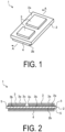
- FIG. 1 is a perspective view illustrating the overall configuration of the circuit board 1 according to the embodiment
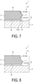
- FIG. 2 is an arrow cross-sectional view taken along an A-A line illustrated in FIG. 1 .
- the circuit board 1 includes a ceramic substrate 2, metal plates 3, and a metal plate 4.
- the circuit board 1 has a structure in which the metal plates 3, the ceramic substrate 2, and the metal plate 4 are layered in this order.
- the ceramic substrate 2 has, for example, a rectangular flat plate shape in a plan view, and includes a front surface 2a that is one main surface and a back surface 2b that is the other main surface.
- the ceramic substrate 2 is not limited to a rectangular shape in a plan view.
- Ceramics configuring the ceramic substrate 2 suitably include, for example, alumina, silica, mullite, cordierite, forsterite, aluminum nitride, silicon nitride, silicon carbide, or glass ceramics.
- the ceramic substrate 2 preferably contains silicon nitride (Si 3 N 4 ) as a main component in terms of its high coefficient of thermal conductivity.
- the terms "containing silicon nitride as a main component" mean that the ceramic substrate 2 contains 70 mass% or more of silicon nitride.
- the coefficient of thermal conductivity of the ceramic substrate 2 is increased.
- a heat dissipation property of the circuit board 1 can be improved.
- the ceramic substrate 2 has a thickness of, for example, about from 0.1 mm to 1 mm, and is appropriately set in accordance with conditions such as predetermined external dimensions and mechanical strength of an electronic device (not illustrated) in which the circuit board 1 is mounted.
- the metal plate 3 is bonded to the front surface 2a of the ceramic substrate 2, and includes a predetermined circuit pattern.
- a predetermined circuit pattern indicate a pattern shape corresponding to an electric circuit configured in an electronic device in which the circuit board 1 is mounted.
- the metal plate 3 includes a mounting surface 3a that is one main surface, a bonding surface 3b that is the other main surface, and an outer peripheral surface 3c.
- the mounting surface 3a is a surface on which electronic components (not illustrated) are mounted
- the bonding surface 3b is a surface bonded to the front surface 2a of the ceramic substrate 2 with a brazing material 5 interposed therebetween.
- metal configuring the metal plate 3 suitably include metal containing copper, silver, aluminum as a main component.
- the metal plate 3 preferably contains copper as a main component in terms of high electric conductivity and a high coefficient of thermal conductivity.
- the terms "containing copper as a main component” mean that the metal plate 3 contains 70 mass% or more of copper.
- the copper contained in the metal plate 3 is equal to or greater than 70 mass%, an allowable current that can flow through the electronic components mounted on the circuit board 1 can be increased.
- the metal plate 4 is bonded to the back surface 2b of the ceramic substrate 2 with a brazing material 5 interposed therebetween.
- the metal plate 4 has, for example, a rectangular shape slightly smaller than the ceramic substrate 2 in a plan view.
- the metal same as, and/or similar to that of the metal plate 3 can be used for the metal plate 4. Note that the shapes of the metal plate 3 and the metal plate 4 are not limited to the examples of FIG. 1 and FIG. 2 .
- the thicknesses of the metal plate 3 and the metal plate 4 are, for example, about from 0.3 mm to 1 mm, and are appropriately set in accordance with conditions such as the predetermined external dimensions and the mechanical strength of the electronic device in which the circuit board 1 is mounted.
- the brazing material 5 is made of, for example, a silver-copper-based or copper-based brazing material.
- the brazing material 5 preferably contains at least one active metal selected from the group consisting of titanium, hafnium, and zirconium. This improves the wettability with respect to the ceramic substrate 2, so that the metal plates 3 and 4 can be firmly bonded to the ceramic substrate 2.
- the brazing material 5 preferably contains at least one type of high melting point metal selected from the group consisting of molybdenum, tungsten, tantalum, and osmium. This can improve shape retainability of the brazing material 5, avoid spread of the brazing material 5 to the surface of the ceramic substrate 2, and improve insulation.
- the brazing material 5 may contain at least one type of a metal material selected from the group consisting of indium and tin. This can lower a melting point of the silver-copper-based brazing material, so that residual stress due to thermal stress generated upon manufacturing the circuit board 1 can be reduced.
- a thickness of the brazing material 5 is, for example, approximately from 5 ⁇ m to 100 ⁇ m.
- FIG. 3 is an enlarged cross-sectional view illustrating a configuration of the circuit board 1 according to the embodiment, and is an enlarged cross-sectional view of the outer peripheral surface 3c of the metal plate 3 and its vicinity.
- the outer peripheral surface 3c of the metal plate 3 includes a protruding portion 11 and a pair of recessed surfaces 12.
- the protruding portion 11 is disposed at a center portion of the metal plate 3 in a thickness direction and protrudes outward.
- a height of the protruding portion 11 is, for example, from 50 ⁇ m to 300 ⁇ m.
- the recessed surface 12 has such a shape that the center portion of the surface is more recessed than at least a part of the peripheral portion of the surface.
- the pair of recessed surfaces 12 includes a recessed surface 12 at a side closer to the ceramic substrate 2 than the protruding portion 11 (hereinafter, also referred to as a recessed surface 12A) and a recessed surface 12 at a side farther from the ceramic substrate 2 than the protruding portion 11 (hereinafter, also referred to as a recessed surface 12B).
- the recessed surface 12A is configured such that the bottom thereof is widened in a direction approaching the ceramic substrate 2 with the protruding portion 11 as a starting point.
- the recessed surface 12B is configured such that the bottom thereof is widened in a direction away from the ceramic substrate 2 with the protruding portion 11 as a starting point.
- providing the protruding portion 11 at the center portion of the outer peripheral surface 3c in the thickness direction causes electric field concentration to occur at the protruding portion 11 separated away from the ceramic substrate 2 at the metal plate 3 applied with a high voltage during an operation of the electronic device.
- providing the pair of the recessed surfaces 12 at both sides of the protruding portion 11 can increase a creepage distance.
- the recessed surface 12A positioned at the lower side has a recessed shape, when the metal plate 3 is bonded by using the brazing material 5, creeping up of the brazing material 5 to the mounting surface 3a can be suppressed.
- interference of the brazing material 5 that has crept up to the mounting surface 3a with electronic components can be suppressed, which allows the circuit board 1 to be easily mounted with the electronic components.
- the cross-section shape of the outer peripheral surface 3c as illustrated in FIG. 3 can be formed by substantially uniformly performing isotropic etching such as wet etching from both main surfaces of the metal plate 3 before bonding the metal plate 3 to the ceramic substrate 2.
- the circuit board 1 according to the embodiment may be formed by bonding the metal plate 3 formed in a predetermined circuit pattern by the isotropic etching to the front surface 2a of the ceramic substrate 2 with the brazing material 5.
- an outer peripheral surface 5a of the brazing material 5 may be disposed at the same position as that of a bottom portion 12Aa of the recessed surface 12A in a plan view.
- an end portion of the metal plate 3 can be suppressed to be a free end.
- the stress concentration on the outer peripheral surface 5a of the brazing material 5 can be suppressed, which can improve mechanical reliability of the circuit board 1.
- the same pattern as the circuit pattern of the metal plate 3 may be printed on the front surface 2a of the ceramic substrate 2 with the brazing material 5, and the metal plate 3 formed with the pattern may be positioned on the printed brazing material 5.
- an amount of carbon and an amount of nitrogen in the outer peripheral portion may be larger than an amount of carbon and an amount of nitrogen in the center portion.
- the outer peripheral portion of the brazing material 5 is, for example, a region within a range being equal to or less than 1 (mm) from the outer peripheral surface 5a of the brazing material 5, and the center portion of the brazing material 5 is a region positioned closer to the center than the outer peripheral portion of the brazing material 5.
- brazing material 5 increasing the amount of carbon and the amount of nitrogen in the outer peripheral portion of the brazing material 5 can reduce fluidity of the brazing material 5 positioned at the outer peripheral portion when the metal plate 3 is bonded by using the brazing material 5.
- protrusion of the brazing material 5 to the recessed surface 12 can be suppressed, which can suppress creeping up of the brazing material 5 to the mounting surface 3a.
- Reducing the amount of carbon and the amount of nitrogen in the center portion of the brazing material 5 can uniformly disperse the brazing material 5.
- thermal resistance of the brazing material 5 can be reduced, and thus, a heat dissipation property of the circuit board 1 can be enhanced.
- Uniformly dispersing the brazing material 5 can enhance adhesion strength between the brazing material 5, and the metal plate 3 and the ceramic substrate 2, so that reliability of the circuit board 1 can be increased.
- the amount of carbon and the amount of nitrogen in the brazing material 5 can be obtained by, for example, analyzing a cut surface of the brazing material 5 by using an electron probe microanalyzer (EPMA).
- EPMA electron probe microanalyzer
- FIG. 4 is an enlarged cross-sectional view illustrating a configuration of the circuit board 1 according to a first variation of the embodiment.
- the outer peripheral surface 5a of the brazing material 5 is disposed at an inner side from the outer peripheral surface 3c of the metal plate 3 (to be specific, the bottom portion 12Aa of the recessed surface 12A).
- a distance between the outer peripheral surface 5a of the brazing material 5 and the outer peripheral surface 3c of the metal plate 3 may be, for example, equal to or less than 200 ⁇ m. This can achieve both the electrical reliability and the mechanical reliability of the circuit board 1.
- FIG. 5 is an enlarged cross-sectional view illustrating a configuration of the circuit board 1 according to a second variation of the embodiment.
- the outer peripheral surface 5a of the brazing material 5 is disposed at an outer side of the bottom portion 12Aa of the recessed surface 12A in the outer peripheral surface 3c of the metal plate 3.
- the brazing material 5 is disposed protruding to the recessed surface 12A at the lower side.
- the amount of carbon and the amount of nitrogen in the brazing material 5 disposed protruding to the recessed surface 12A of the metal plate 3 may be larger than the amount of carbon and the amount of nitrogen in the brazing material 5 disposed between the metal plate 3 and the ceramic substrate 2.
- protrusion of the brazing material 5 to the recessed surface 12B can be suppressed, which can suppress creeping up of the brazing material 5 to the mounting surface 3a.
- Reducing the amount of carbon and the amount of nitrogen in the brazing material 5 disposed between the metal plate 3 and the ceramic substrate 2 can uniformly disperse the brazing material 5.
- thermal resistance of the brazing material 5 can be reduced, which can enhance a heat dissipation property of the circuit board 1.
- Uniformly dispersing the brazing material 5 can enhance adhesion strength between the brazing material 5, and the metal plate 3 and the ceramic substrate 2, so that reliability of the circuit board 1 can be increased.
- FIG. 6 is an enlarged cross-sectional view illustrating a configuration of the circuit board 1 according to a third variation of the embodiment.
- the brazing material 5 disposed protruding to the recessed surface 12A is disposed in a manner that the brazing material on the protruding portion 11 side is further outside than the brazing material on the ceramic substrate 2 side.
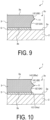
- FIG. 7 is an enlarged cross-sectional view illustrating a configuration of the circuit board 1 according to the fourth variation of the embodiment. As illustrated in FIG. 7 , in a fourth variation, the brazing material 5 is disposed protruding to both the recessed surface 12A at the lower side and the recessed surface 12B at the upper side.
- the brazing material 5 may be disposed such that the brazing material 5 does not adhere to a tip end portion of the protruding portion 11. This can suppress a decrease in the distance between the metal plates 3 adjacent to each other due to the brazing material 5 adhering to the tip end portion.
- the brazing material 5 is not attached to the tip end portion of the protruding portion 11, which can suppress the occurrence of the ion migration phenomenon caused by the brazing material 5 in the protruding portion 11. Consequently, according to the fourth variation, electrical reliability of the circuit board 1 can be improved.
- FIG. 8 is an enlarged cross-sectional view illustrating a configuration of the circuit board 1 according to a fifth variation of the embodiment.
- the protruding portion 11 is disposed closer to the ceramic substrate 2 side (the bonding surface 3b side) than the center portion of the metal plate 3 in the thickness direction.
- a radius of curvature of the recessed surface 12B at the upper side is larger than a radius of curvature of the recessed surface 12A at the lower side.
- the cross-section shape of the outer peripheral surface 3c as illustrated in FIG. 8 can be formed by etching the mounting surface 3a side more deeply than the bonding surface 3b side when isotropic etching is performed from both main surfaces of the metal plate 3.
- FIG. 9 is an enlarged cross-sectional view illustrating a configuration of the circuit board 1 according to a sixth variation of the embodiment.
- the protruding portion 11 is disposed closer to the mounting surface 3a side than the center portion of the metal plate 3 in the thickness direction.
- a radius of curvature of the recessed surface 12A at the lower side is larger than a radius of curvature of the recessed surface 12B at the upper side.
- creeping up of the brazing material 5 to the tip end portion of the protruding portion 11 can be suppressed, which allows the occurrence of the ion migration phenomenon caused by the brazing material 5 to be suppressed in the protruding portion 11.
- FIG. 10 is an enlarged cross-sectional view illustrating a configuration of the circuit board 1 according to a seventh variation of the embodiment.
- the outer peripheral surface 3c of the metal plate 3 includes different protruding portions 13 and 14.
- the protruding portion 13 is positioned at a side closer to the ceramic substrate 2 than the protruding portion 11, and the protruding portion 14 is positioned at a side farther from the ceramic substrate 2 than the protruding portion 11.
- the different protruding portion 13 is provided at the bottom portion 12Aa of the recessed surface 12A, and the different protruding portion 14 is provided at a bottom portion 12Ba of the recessed surface 12B.
- the recessed surface 12A has a recessed shape with a large curvature, when the metal plate 3 is bonded with the brazing material 5, creeping up of the brazing material 5 to the tip end portion of the protruding portion 11 can be further suppressed.
- the occurrence of the ion migration phenomenon caused by the brazing material 5 can be further suppressed in the protruding portion 11.
- FIG. 11 is an enlarged cross-sectional view illustrating a configuration of the circuit board 1 according to an eighth variation of the embodiment. As illustrated in FIG. 11 , the eighth variation is different from the embodiment in a point that a metal pin 6 is erected through the metal plate 3. To be specific, a through hole 3d is formed at a predetermined position of the metal plate 3, and the metal pin 6 is inserted into the through hole 3d, so that the metal pin 6 is erected through the metal plate 3.
- metal constituting the metal pin 6 for example, metal containing copper, silver, aluminum, an alloy of these metals, or the like as a main component is suitably used.
- the metal pin 6 preferably contains copper that is the same material as that of the metal plate as a main component from the viewpoint of achieving the same linear expansion coefficient.
- the metal pin 6 may be fixed to the metal plate 3 by using the brazing material 5.
- the metal pin 6 and the metal plate 3 can be electrically connected to each other through the brazing material 5.
- electrical resistance between the metal pin 6 and the metal plate 3 can be reduced as compared with the case where the metal plate 3 and the metal pin 6 are electrically connected to each other by fitting the metal pin 6 to the metal plate 3.
- the metal pin 6 is fixed by using a solder material instead of the brazing material 5, in the eighth variation, melting and damaging of the bonding portion of the metal pin 6 can be suppressed when the electronic device is used in a high-temperature environment. This is because the brazing material 5 has a higher melting point than that of the solder material.
- the metal pin 6 is fixed by using the solder material instead of the brazing material 5, a process of soldering the metal pin 6 is additionally required.
- the metal plate 3 and the metal pin 6 can be collectively fixed by using the brazing material 5, the manufacturing process of the circuit board 1 can be simplified.
- thermal resistance of the circuit board 1 can be improved, and a manufacturing cost of the circuit board 1 can be reduced.
- the metal pin 6 may be in contact with the brazing material 5 not only at the portion protruding downward from the metal plate 3 but also in the through hole 3d of the metal plate 3. That is, in the eighth variation, the brazing material 5 may include a creep-up portion 5b that creeps up a gap between the metal plate 3 and the metal pin 6 in the through hole 3d.
- a contact area between the metal pin 6 and the brazing material 5 can be increased, which allows electrical resistance between the metal pin 6 and the metal plate 3 to be further reduced.
- an allowable current that can flow through the electronic component mounted on the circuit board 1 can be further increased.
- the creep-up portion 5b can be formed by inserting the metal pin 6 so as to press the brazing material 5 from above upon inserting the metal pin 6 into the through hole 3d after placing the metal plate 3 on the brazing material 5 printed on the ceramic substrate 2.
- the through hole 3d of the metal plate 3 can be formed by substantially uniformly performing isotropic etching from both main surfaces of the metal plate 3 when the metal plate 3 is formed into a predetermined circuit pattern.
- FIG. 12 is an enlarged cross-sectional view illustrating a configuration of the circuit board 1 according to a ninth variation of the embodiment.
- the metal plate 3 is bonded to the ceramic substrate 2 by using the brazing material 5 in the embodiment and the various variations that have been described above, the metal plate 3 may be directly bonded to the ceramic substrate 2 as illustrated in FIG. 12 .
- the metal plate 3 containing copper as a main component is directly bonded to the front surface 2a of the ceramic substrate 2 by using a eutectic phase such as Cu-Cu 2 O.
- the metal plate 3 containing aluminum as a main component may be directly bonded to the front surface 2a of the ceramic substrate 2 containing silicon nitride as a main component by using an Al-Si eutectic phase.
- the protruding portion 11 is provided at the center portion of the outer peripheral surface 3c in the thickness direction.
- electric field concentration can be generated at the protruding portion 11 separated from the ceramic substrate 2.
- providing the pair of recessed surfaces 12 at both sides of the protruding portion 11 can increase a creepage distance.
- the ninth variation even when a high voltage is applied during an operation of the electronic device, concentration of an electric field at the ceramic substrate 2 can be suppressed, which can suppress dielectric breakdown of the ceramic substrate 2.
- concentration of an electric field at the ceramic substrate 2 can be suppressed, which can suppress dielectric breakdown of the ceramic substrate 2.
- reliability of the electronic device in which the circuit board 1 is mounted can be improved.
- FIG. 13 is a flowchart illustrating a procedure of a manufacturing process for the circuit board 1 according to the embodiment.
- Step S101 the ceramic substrate 2 having a flat plate shape is prepared. Note that, in Step S101, blank baking of the ceramic substrate 2 or the like is performed as necessary.
- a predetermined circuit pattern is printed on the front surface 2a of the prepared ceramic substrate 2 with the brazing material 5 containing active metal (Step S102).
- the brazing material 5 containing the active metal is printed in a substantially rectangular shape on the back surface 2b of the ceramic substrate 2 (Step S103).
- processing in Step S103 may be performed prior to processing in Step S102, or may be simultaneously performed with processing in Step S102.
- the metal plate 3 is formed by shaping a metal plate serving as a raw material into a predetermined circuit pattern by isotropic etching from both surfaces, and the metal plate 4 is formed by shaping a metal plate serving as a raw material into a rectangular shape (Step S104).
- the protruding portion 11 and the pair of recessed surfaces 12 are formed at the outer peripheral surface 3c of the metal plate 3 in the processing of Step S104.
- the metal plates 3 and the metal plate 4 are disposed on the surfaces of the brazing material 5 printed on the front surface 2a and the back surface 2b of the ceramic substrate 2, respectively (Step S105).
- the metal plates 3 and the metal plate 4 are disposed on the surfaces of the brazing material 5 while the printed shapes of the brazing material 5 and the shapes of the metal plates 3 and the metal plate 4 are positioned so as to overlap each other.
- the brazing material 5 is heated to a melting temperature or higher and melted, which bonds the metal plates 3 and the metal plate 4 that are disposed on the surfaces of the brazing material 5 to the front surface 2a and the back surface 2b of the ceramic substrate 2 with the brazing material 5 (Step S106).
- an etching process of the brazing material does not need to be additionally performed.
- the process can be simplified and a decrease in electrical reliability can be suppressed due to a residue of the etched brazing material.
- the brazing material 5 may be heated in a vacuum or an inert atmosphere such as nitrogen gas or argon gas in the processing of Step S106. This allows the brazing material 5 positioned at the outer peripheral portion (or protruding to the recessed surface 12A) to be more exposed to carbon and nitrogen in the atmosphere than the brazing material 5 positioned at the center portion (or disposed between the metal plate 3 and the ceramic substrate 2).
- an amount of carbon and an amount of nitrogen in the brazing material 5 positioned at the outer peripheral portion (or protruding to the recessed surface 12A) can be made larger than an amount of carbon and an amount of nitrogen in the brazing material 5 positioned at the center portion (or disposed between the metal plate 3 and the ceramic substrate 2).
- the ceramic substrate 2 bonded with the metal plate 3 and the metal plate 4 is subjected to a laser beam machining process, a chemical polishing process, a rust proofing process, or the like as necessary to complete the manufacturing process of the circuit board 1 according to the embodiment.
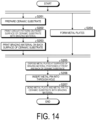
- FIG. 14 is a flowchart illustrating a procedure of a manufacturing process for the circuit board 1 according to the eighth variation of the embodiment. As illustrated in FIG. 14 , in the manufacturing process, first, the ceramic substrate 2 having a flat plate shape is prepared (Step S201).
- a predetermined circuit pattern is printed on the front surface 2a of the prepared ceramic substrate 2 with the brazing material 5 containing active metal (Step S202).
- the brazing material 5 containing the active metal is printed in a substantially rectangular shape on the back surface 2b of the ceramic substrate 2 (Step S203).
- the metal plate 3 is formed by shaping a metal plate serving as a raw material into a predetermined circuit pattern by isotropic etching from both surfaces, and the metal plate 4 is formed by shaping a metal plate serving as a raw material into a rectangular shape (Step S204).
- the protruding portion 11 and the pair of recessed surfaces 12 are formed at the outer peripheral surface 3c of the metal plate 3, and the through hole 3d through which the metal pin 6 is inserted is formed.
- the metal plates 3 and the metal plate 4 are disposed on the surfaces of the brazing material 5 printed on the front surface 2a and the back surface 2b of the ceramic substrate 2, respectively (Step S205). In the processing of Step S205, the metal plates 3 and the metal plate 4 are disposed on the surfaces of the brazing material 5 while the printed shapes of the brazing material 5 and the shapes of the metal plates 3 and the metal plate 4 are positioned so as to overlap each other.
- the metal pin 6 is inserted into the through hole 3d formed in the metal plate 3 (Step S206).
- the creep-up portion 5b in the brazing material 5 may be preferably formed by inserting the metal pin 6 so as to press the brazing material 5 from above.
- the brazing material 5 is heated to a melting temperature or higher and melted, so that the metal plates 3, the metal plate 4, and the metal pin 6 that are disposed on the surfaces of the brazing material 5 are bonded to the front surface 2a and the back surface 2b of the ceramic substrate 2 with the brazing material 5 (Step S207).
- the ceramic substrate 2 bonded with the metal plates 3, the metal plate 4, and the metal pin 6 is subjected to a laser beam machining process, a chemical polishing process, a rust proofing process, or the like as necessary to complete the manufacturing process of the circuit board 1 according to the eighth variation.
- the present invention has been described above. However, the present invention is not limited to the embodiment described above, and various modifications can be made without departing from the essential spirit of the present invention.
- the ceramic substrate 2 and the metal plates 3 and 4 are layered to form the circuit board 1, but the metal plate 4 at the back surface side may be omitted.
Landscapes
- Engineering & Computer Science (AREA)
- Chemical & Material Sciences (AREA)
- Microelectronics & Electronic Packaging (AREA)
- Ceramic Engineering (AREA)
- Manufacturing & Machinery (AREA)
- Materials Engineering (AREA)
- Structural Engineering (AREA)
- Organic Chemistry (AREA)
- Structure Of Printed Boards (AREA)
- Cooling Or The Like Of Semiconductors Or Solid State Devices (AREA)
- Manufacturing Of Printed Wiring (AREA)
Abstract
Description
- An embodiment of the disclosure relates to a circuit board and a manufacturing method for a circuit board.
- Examples of a known circuit board used for an electronic device in which an electronic component such as a power semiconductor element is mounted include a circuit board in which a metal plate including a circuit pattern is bonded to a main surface of a ceramic substrate (see, for example, Patent Document 1).
- Patent Document 1:
JP 2001-332854 A - However, the known art has room for further enhancement in terms of improving reliability of the electronic device.
- In light of the foregoing, an object of an aspect of the embodiment is to provide a circuit board that can provide improved reliability of an electronic device, and a manufacturing method for the circuit board.
- In an aspect of an embodiment, a circuit board includes a ceramic substrate having a flat plate shape and a metal plate bonded to one main surface of the ceramic substrate and including a predetermined circuit pattern. An outer peripheral surface of the metal plate includes a protruding portion protruding outward and a pair of recessed surfaces provided at both sides of the protruding portion.
-
-
FIG. 1 is a perspective view illustrating an overall configuration of a circuit board according to an embodiment. -
FIG. 2 is an arrow cross-sectional view taken along an A-A line illustrated inFIG. 1 . -
FIG. 3 is an enlarged cross-sectional view illustrating a configuration of the circuit board according to the embodiment. -
FIG. 4 is an enlarged cross-sectional view illustrating a configuration of a circuit board according to a first variation of the embodiment. -
FIG. 5 is an enlarged cross-sectional view illustrating a configuration of a circuit board according to a second variation of the embodiment. -
FIG. 6 is an enlarged cross-sectional view illustrating a configuration of a circuit board according to a third variation of the embodiment. -
FIG. 7 is an enlarged cross-sectional view illustrating a configuration of a circuit board according to a fourth variation of the embodiment. -
FIG. 8 is an enlarged cross-sectional view illustrating a configuration of a circuit board according to a fifth variation of the embodiment. -
FIG. 9 is an enlarged cross-sectional view illustrating a configuration of a circuit board according to a sixth variation of the embodiment. -
FIG. 10 is an enlarged cross-sectional view illustrating a configuration of a circuit board according to a seventh variation of the embodiment. -
FIG. 11 is an enlarged cross-sectional view illustrating a configuration of a circuit board according to an eighth variation of the embodiment. -
FIG. 12 is an enlarged cross-sectional view illustrating a configuration of a circuit board according to a ninth variation of the embodiment. -
FIG. 13 is a flowchart illustrating a procedure of a manufacturing process for a circuit board according to the embodiment. -
FIG. 14 is a flowchart illustrating a procedure of a manufacturing process for the circuit board according to the eighth variation of the embodiment. - Hereinafter, an embodiment of a circuit board and a manufacturing method for a circuit board that are disclosed in the present application will be described with reference to the accompanying drawings. The present invention is not limited by the following embodiment.
- Examples of a known circuit board used for an electronic device in which an electronic component such as a power semiconductor element is mounted include a circuit board in which a metal plate including a circuit pattern is bonded to a main surface of a ceramic substrate.
- However, the known art has room for further enhancement in terms of improving reliability of the electronic device. For example, the known art may cause dielectric breakdown of the ceramic substrate when electric field is concentrated at the outer peripheral portion of the metal plate applied with a high voltage.
- The achievement of a technique that can overcome the aforementioned problem and improve reliability of an electronic device is awaited.
- First, an overall configuration of a
circuit board 1 according to the embodiment will be described with reference toFIG. 1 and FIG. 2. FIG. 1 is a perspective view illustrating the overall configuration of thecircuit board 1 according to the embodiment, andFIG. 2 is an arrow cross-sectional view taken along an A-A line illustrated inFIG. 1 . - As illustrated in
FIG. 1 , thecircuit board 1 according to the embodiment includes aceramic substrate 2,metal plates 3, and ametal plate 4. Thecircuit board 1 has a structure in which themetal plates 3, theceramic substrate 2, and themetal plate 4 are layered in this order. - The
ceramic substrate 2 has, for example, a rectangular flat plate shape in a plan view, and includes afront surface 2a that is one main surface and aback surface 2b that is the other main surface. However, in the present disclosure, theceramic substrate 2 is not limited to a rectangular shape in a plan view. - Examples of ceramics configuring the
ceramic substrate 2 suitably include, for example, alumina, silica, mullite, cordierite, forsterite, aluminum nitride, silicon nitride, silicon carbide, or glass ceramics. Theceramic substrate 2 preferably contains silicon nitride (Si3N4) as a main component in terms of its high coefficient of thermal conductivity. - Here, the terms "containing silicon nitride as a main component" mean that the
ceramic substrate 2 contains 70 mass% or more of silicon nitride. When the silicon nitride contained in theceramic substrate 2 is equal to or greater than 70 mass%, the coefficient of thermal conductivity of theceramic substrate 2 is increased. Thus, a heat dissipation property of thecircuit board 1 can be improved. - The
ceramic substrate 2 has a thickness of, for example, about from 0.1 mm to 1 mm, and is appropriately set in accordance with conditions such as predetermined external dimensions and mechanical strength of an electronic device (not illustrated) in which thecircuit board 1 is mounted. - The
metal plate 3 is bonded to thefront surface 2a of theceramic substrate 2, and includes a predetermined circuit pattern. The terms "a predetermined circuit pattern" indicate a pattern shape corresponding to an electric circuit configured in an electronic device in which thecircuit board 1 is mounted. - As illustrated in
FIG. 2 , themetal plate 3 includes amounting surface 3a that is one main surface, abonding surface 3b that is the other main surface, and an outerperipheral surface 3c. Themounting surface 3a is a surface on which electronic components (not illustrated) are mounted, and thebonding surface 3b is a surface bonded to thefront surface 2a of theceramic substrate 2 with a brazingmaterial 5 interposed therebetween. - Examples of metal configuring the
metal plate 3 suitably include metal containing copper, silver, aluminum as a main component. Themetal plate 3 preferably contains copper as a main component in terms of high electric conductivity and a high coefficient of thermal conductivity. - Here, the terms "containing copper as a main component" mean that the
metal plate 3 contains 70 mass% or more of copper. When the copper contained in themetal plate 3 is equal to or greater than 70 mass%, an allowable current that can flow through the electronic components mounted on thecircuit board 1 can be increased. - The
metal plate 4 is bonded to theback surface 2b of theceramic substrate 2 with a brazingmaterial 5 interposed therebetween. Themetal plate 4 has, for example, a rectangular shape slightly smaller than theceramic substrate 2 in a plan view. The metal same as, and/or similar to that of themetal plate 3 can be used for themetal plate 4. Note that the shapes of themetal plate 3 and themetal plate 4 are not limited to the examples ofFIG. 1 and FIG. 2 . - The thicknesses of the
metal plate 3 and themetal plate 4 are, for example, about from 0.3 mm to 1 mm, and are appropriately set in accordance with conditions such as the predetermined external dimensions and the mechanical strength of the electronic device in which thecircuit board 1 is mounted. - The
brazing material 5 is made of, for example, a silver-copper-based or copper-based brazing material. Thebrazing material 5 preferably contains at least one active metal selected from the group consisting of titanium, hafnium, and zirconium. This improves the wettability with respect to theceramic substrate 2, so that themetal plates ceramic substrate 2. - The
brazing material 5 preferably contains at least one type of high melting point metal selected from the group consisting of molybdenum, tungsten, tantalum, and osmium. This can improve shape retainability of the brazingmaterial 5, avoid spread of the brazingmaterial 5 to the surface of theceramic substrate 2, and improve insulation. - The
brazing material 5 may contain at least one type of a metal material selected from the group consisting of indium and tin. This can lower a melting point of the silver-copper-based brazing material, so that residual stress due to thermal stress generated upon manufacturing thecircuit board 1 can be reduced. A thickness of thebrazing material 5 is, for example, approximately from 5 µm to 100 µm. - Details of the configuration of the
circuit board 1 according to the embodiment will be described with reference toFIG. 3. FIG. 3 is an enlarged cross-sectional view illustrating a configuration of thecircuit board 1 according to the embodiment, and is an enlarged cross-sectional view of the outerperipheral surface 3c of themetal plate 3 and its vicinity. - As illustrated in
FIG. 3 , the outerperipheral surface 3c of themetal plate 3 includes a protrudingportion 11 and a pair of recessed surfaces 12. The protrudingportion 11 is disposed at a center portion of themetal plate 3 in a thickness direction and protrudes outward. A height of the protrudingportion 11 is, for example, from 50 µm to 300 µm. - The recessed
surface 12 has such a shape that the center portion of the surface is more recessed than at least a part of the peripheral portion of the surface. The pair of recessedsurfaces 12 includes a recessedsurface 12 at a side closer to theceramic substrate 2 than the protruding portion 11 (hereinafter, also referred to as a recessedsurface 12A) and a recessedsurface 12 at a side farther from theceramic substrate 2 than the protruding portion 11 (hereinafter, also referred to as a recessedsurface 12B). - The recessed
surface 12A is configured such that the bottom thereof is widened in a direction approaching theceramic substrate 2 with the protrudingportion 11 as a starting point. The recessedsurface 12B is configured such that the bottom thereof is widened in a direction away from theceramic substrate 2 with the protrudingportion 11 as a starting point. - In the embodiment, providing the protruding
portion 11 at the center portion of the outerperipheral surface 3c in the thickness direction causes electric field concentration to occur at the protrudingportion 11 separated away from theceramic substrate 2 at themetal plate 3 applied with a high voltage during an operation of the electronic device. - In the embodiment, providing the pair of the recessed surfaces 12 at both sides of the protruding
portion 11 can increase a creepage distance. - That is, in the embodiment, even when a high voltage is applied during an operation of the electronic device, concentration of an electric field on the
ceramic substrate 2 can be suppressed. Thus, dielectric breakdown of theceramic substrate 2 can be suppressed. Thus, according to the embodiment, reliability of the electronic device on which thecircuit board 1 is mounted can be improved. - In the embodiment, even when an ion migration phenomenon occurs at the protruding
portion 11 due to the electric field concentration, a creepage distance to the outerperipheral surface 3c of theadjacent metal plate 3 can be extended by the recessedsurface 12A positioned at the lower side. Thus, according to the embodiment, a short circuit between themetal plates 3 can be suppressed due to the ion migration phenomenon. - In the embodiment, the recessed
surface 12A positioned at the lower side has a recessed shape, when themetal plate 3 is bonded by using thebrazing material 5, creeping up of thebrazing material 5 to the mountingsurface 3a can be suppressed. - Thus, according to the embodiment, interference of the
brazing material 5 that has crept up to the mountingsurface 3a with electronic components can be suppressed, which allows thecircuit board 1 to be easily mounted with the electronic components. - Note that the cross-section shape of the outer
peripheral surface 3c as illustrated inFIG. 3 can be formed by substantially uniformly performing isotropic etching such as wet etching from both main surfaces of themetal plate 3 before bonding themetal plate 3 to theceramic substrate 2. - That is, the
circuit board 1 according to the embodiment may be formed by bonding themetal plate 3 formed in a predetermined circuit pattern by the isotropic etching to thefront surface 2a of theceramic substrate 2 with thebrazing material 5. - In the embodiment, an outer
peripheral surface 5a of thebrazing material 5 may be disposed at the same position as that of a bottom portion 12Aa of the recessedsurface 12A in a plan view. Thus, an end portion of themetal plate 3 can be suppressed to be a free end. - Thus, according to the embodiment, the stress concentration on the outer
peripheral surface 5a of thebrazing material 5 can be suppressed, which can improve mechanical reliability of thecircuit board 1. - Note that in order to dispose the outer
peripheral surface 3c of thebrazing material 5 and the bottom portion 12Aa of the recessedsurface 12A at the same position in a plan view, the same pattern as the circuit pattern of themetal plate 3 may be printed on thefront surface 2a of theceramic substrate 2 with thebrazing material 5, and themetal plate 3 formed with the pattern may be positioned on the printedbrazing material 5. - In the embodiment, in the
brazing material 5 disposed between themetal plate 3 and theceramic substrate 2, an amount of carbon and an amount of nitrogen in the outer peripheral portion may be larger than an amount of carbon and an amount of nitrogen in the center portion. Here, the outer peripheral portion of thebrazing material 5 is, for example, a region within a range being equal to or less than 1 (mm) from the outerperipheral surface 5a of thebrazing material 5, and the center portion of thebrazing material 5 is a region positioned closer to the center than the outer peripheral portion of thebrazing material 5. - In this way, increasing the amount of carbon and the amount of nitrogen in the outer peripheral portion of the
brazing material 5 can reduce fluidity of thebrazing material 5 positioned at the outer peripheral portion when themetal plate 3 is bonded by using thebrazing material 5. - Thus, according to the embodiment, protrusion of the
brazing material 5 to the recessedsurface 12 can be suppressed, which can suppress creeping up of thebrazing material 5 to the mountingsurface 3a. - Reducing the amount of carbon and the amount of nitrogen in the center portion of the
brazing material 5 can uniformly disperse thebrazing material 5. Thus, according to the embodiment, thermal resistance of thebrazing material 5 can be reduced, and thus, a heat dissipation property of thecircuit board 1 can be enhanced. Uniformly dispersing thebrazing material 5 can enhance adhesion strength between thebrazing material 5, and themetal plate 3 and theceramic substrate 2, so that reliability of thecircuit board 1 can be increased. - Note that in the present disclosure, the amount of carbon and the amount of nitrogen in the
brazing material 5 can be obtained by, for example, analyzing a cut surface of thebrazing material 5 by using an electron probe microanalyzer (EPMA). - Various variations of the embodiment will be described with reference to
FIG. 4 to FIG. 12 . Note that, in the various variations below, portions that are the same as those in the embodiment will be denoted by the same reference signs, and redundant explanations may be omitted. -
FIG. 4 is an enlarged cross-sectional view illustrating a configuration of thecircuit board 1 according to a first variation of the embodiment. As illustrated inFIG. 4 , in the first variation, the outerperipheral surface 5a of thebrazing material 5 is disposed at an inner side from the outerperipheral surface 3c of the metal plate 3 (to be specific, the bottom portion 12Aa of the recessedsurface 12A). - Thus, a distance between the protruding
portion 11 and thebrazing material 5 where electric field concentration occurs can be increased, so that the occurrence of the ion migration phenomenon caused by thebrazing material 5 can be suppressed in the protrudingportion 11. Consequently, according to the first variation, electrical reliability of thecircuit board 1 can be improved. - Note that a distance between the outer
peripheral surface 5a of thebrazing material 5 and the outerperipheral surface 3c of themetal plate 3 may be, for example, equal to or less than 200 µm. This can achieve both the electrical reliability and the mechanical reliability of thecircuit board 1. -
FIG. 5 is an enlarged cross-sectional view illustrating a configuration of thecircuit board 1 according to a second variation of the embodiment. As illustrated inFIG. 4 , in the second variation, the outerperipheral surface 5a of thebrazing material 5 is disposed at an outer side of the bottom portion 12Aa of the recessedsurface 12A in the outerperipheral surface 3c of themetal plate 3. In the second variation, thebrazing material 5 is disposed protruding to the recessedsurface 12A at the lower side. - Thus, in the
metal plate 3, not only thebonding surface 3b but also the recessedsurface 12A are in contact with thebrazing material 5, so that an adhesion force of themetal plate 3 to theceramic substrate 2 is increased. Consequently, according to the second variation, mechanical reliability of thecircuit board 1 can be improved. - In the second variation, the amount of carbon and the amount of nitrogen in the
brazing material 5 disposed protruding to the recessedsurface 12A of themetal plate 3 may be larger than the amount of carbon and the amount of nitrogen in thebrazing material 5 disposed between themetal plate 3 and theceramic substrate 2. - In this way, increasing the amount of carbon and the amount of nitrogen in the
brazing material 5 disposed protruding to the recessedsurface 12A can reduce fluidity of thebrazing material 5 protruding to the recessedsurface 12A when themetal plate 3 is bonded with thebrazing material 5. - Thus, according to the second variation, protrusion of the
brazing material 5 to the recessedsurface 12B can be suppressed, which can suppress creeping up of thebrazing material 5 to the mountingsurface 3a. - Reducing the amount of carbon and the amount of nitrogen in the
brazing material 5 disposed between themetal plate 3 and theceramic substrate 2 can uniformly disperse thebrazing material 5. Thus, according to the second variation, thermal resistance of thebrazing material 5 can be reduced, which can enhance a heat dissipation property of thecircuit board 1. Uniformly dispersing thebrazing material 5 can enhance adhesion strength between thebrazing material 5, and themetal plate 3 and theceramic substrate 2, so that reliability of thecircuit board 1 can be increased. -
FIG. 6 is an enlarged cross-sectional view illustrating a configuration of thecircuit board 1 according to a third variation of the embodiment. As illustrated inFIG. 6 , in the third variation, thebrazing material 5 disposed protruding to the recessedsurface 12A is disposed in a manner that the brazing material on the protrudingportion 11 side is further outside than the brazing material on theceramic substrate 2 side. - This makes it possible to increase an adhesion force of the
metal plate 3 to theceramic substrate 2 while concentrating an electric field on the protrudingportion 11 during an operation of the electronic device. Thus, according to the third variation, both the electrical reliability and the mechanical reliability of thecircuit board 1 can be achieved. -
FIG. 7 is an enlarged cross-sectional view illustrating a configuration of thecircuit board 1 according to the fourth variation of the embodiment. As illustrated inFIG. 7 , in a fourth variation, thebrazing material 5 is disposed protruding to both the recessedsurface 12A at the lower side and the recessedsurface 12B at the upper side. - Thus, in the
metal plate 3, not only thebonding surface 3b but also the recessedsurface 12A and the recessedsurface 12B are in contact with thebrazing material 5, so that an adhesion force of themetal plate 3 to theceramic substrate 2 is further increased. Consequently, according to the fourth variation, mechanical reliability of thecircuit board 1 can be improved. - In the fourth variation, as illustrated in
FIG. 7 , thebrazing material 5 may be disposed such that thebrazing material 5 does not adhere to a tip end portion of the protrudingportion 11. This can suppress a decrease in the distance between themetal plates 3 adjacent to each other due to thebrazing material 5 adhering to the tip end portion. - The
brazing material 5 is not attached to the tip end portion of the protrudingportion 11, which can suppress the occurrence of the ion migration phenomenon caused by thebrazing material 5 in the protrudingportion 11. Consequently, according to the fourth variation, electrical reliability of thecircuit board 1 can be improved. -
FIG. 8 is an enlarged cross-sectional view illustrating a configuration of thecircuit board 1 according to a fifth variation of the embodiment. As illustrated inFIG. 8 , in the fifth variation, the protrudingportion 11 is disposed closer to theceramic substrate 2 side (thebonding surface 3b side) than the center portion of themetal plate 3 in the thickness direction. In the fifth variation, a radius of curvature of the recessedsurface 12B at the upper side is larger than a radius of curvature of the recessedsurface 12A at the lower side. - This makes it possible to reduce a residual stress generated at the end portion of the
metal plate 3 when a temperature is lowered after the brazing process. This is because configuring the end portion of themetal plate 3 as illustrated inFIG. 8 causes a volume itself of the metal positioned at the end portion of themetal plate 3 to be reduced, and causes a residual stress generated in a vertically upward direction to be dispersed by the recessedsurface 12A diagonally disposed. - Consequently, according to the fifth variation, mechanical reliability of the
circuit board 1 can be improved. Note that the cross-section shape of the outerperipheral surface 3c as illustrated inFIG. 8 can be formed by etching the mountingsurface 3a side more deeply than thebonding surface 3b side when isotropic etching is performed from both main surfaces of themetal plate 3. -
FIG. 9 is an enlarged cross-sectional view illustrating a configuration of thecircuit board 1 according to a sixth variation of the embodiment. As illustrated inFIG. 9 , in the sixth variation, the protrudingportion 11 is disposed closer to the mountingsurface 3a side than the center portion of themetal plate 3 in the thickness direction. In the fifth variation, a radius of curvature of the recessedsurface 12A at the lower side is larger than a radius of curvature of the recessedsurface 12B at the upper side. - As a result, in the
metal plate 3 applied with a high voltage during an operation of the electronic device, electric field concentration can be generated at the protrudingportion 11 that is further away from theceramic substrate 2, so that dielectric breakdown of theceramic substrate 2 can be further suppressed. - In the sixth variation, creeping up of the
brazing material 5 to the tip end portion of the protrudingportion 11 can be suppressed, which allows the occurrence of the ion migration phenomenon caused by thebrazing material 5 to be suppressed in the protrudingportion 11. - Consequently, according to the sixth variation, electrical reliability of the
circuit board 1 can be improved. -
FIG. 10 is an enlarged cross-sectional view illustrating a configuration of thecircuit board 1 according to a seventh variation of the embodiment. As illustrated inFIG. 10 , in the seventh variation, the outerperipheral surface 3c of themetal plate 3 includes different protrudingportions portion 13 is positioned at a side closer to theceramic substrate 2 than the protrudingportion 11, and the protrudingportion 14 is positioned at a side farther from theceramic substrate 2 than the protrudingportion 11. - The different protruding
portion 13 is provided at the bottom portion 12Aa of the recessedsurface 12A, and the different protrudingportion 14 is provided at a bottom portion 12Ba of the recessedsurface 12B. - Thus, when not only the
bonding surface 3b but also the recessedsurface 12A of themetal plate 3 are in contact with thebrazing material 5, a contact area between the recessedsurface 12A and thebrazing material 5 can be further increased. Thus, according to the seventh variation, an adhesion force of themetal plate 3 to theceramic substrate 2 is further increased, which can further improve mechanical reliability of thecircuit board 1. - In the seventh variation, the recessed
surface 12A has a recessed shape with a large curvature, when themetal plate 3 is bonded with thebrazing material 5, creeping up of thebrazing material 5 to the tip end portion of the protrudingportion 11 can be further suppressed. - As a result, according to the seventh variation, the occurrence of the ion migration phenomenon caused by the
brazing material 5 can be further suppressed in the protrudingportion 11. -
FIG. 11 is an enlarged cross-sectional view illustrating a configuration of thecircuit board 1 according to an eighth variation of the embodiment. As illustrated inFIG. 11 , the eighth variation is different from the embodiment in a point that ametal pin 6 is erected through themetal plate 3. To be specific, a throughhole 3d is formed at a predetermined position of themetal plate 3, and themetal pin 6 is inserted into the throughhole 3d, so that themetal pin 6 is erected through themetal plate 3. - As metal constituting the
metal pin 6, for example, metal containing copper, silver, aluminum, an alloy of these metals, or the like as a main component is suitably used. Themetal pin 6 preferably contains copper that is the same material as that of the metal plate as a main component from the viewpoint of achieving the same linear expansion coefficient. - Here, in the eighth variation, the
metal pin 6 may be fixed to themetal plate 3 by using thebrazing material 5. Thus, themetal pin 6 and themetal plate 3 can be electrically connected to each other through thebrazing material 5. - In the eighth variation, electrical resistance between the
metal pin 6 and themetal plate 3 can be reduced as compared with the case where themetal plate 3 and themetal pin 6 are electrically connected to each other by fitting themetal pin 6 to themetal plate 3. - Thus, according to the eighth variation, damage to the periphery of the
metal pin 6 can be suppressed when a large current flows through the electronic component, which allows an allowable current that can flow through the electronic component mounted on thecircuit board 1 to be increased. - Compared to a case where the
metal pin 6 is fixed by using a solder material instead of thebrazing material 5, in the eighth variation, melting and damaging of the bonding portion of themetal pin 6 can be suppressed when the electronic device is used in a high-temperature environment. This is because thebrazing material 5 has a higher melting point than that of the solder material. - When the
metal pin 6 is fixed by using the solder material instead of thebrazing material 5, a process of soldering themetal pin 6 is additionally required. On the other hand, in the eighth variation, themetal plate 3 and themetal pin 6 can be collectively fixed by using thebrazing material 5, the manufacturing process of thecircuit board 1 can be simplified. - Thus, according to the eighth variation, thermal resistance of the
circuit board 1 can be improved, and a manufacturing cost of thecircuit board 1 can be reduced. - In the eighth variation, as illustrated in
FIG. 11 , themetal pin 6 may be in contact with thebrazing material 5 not only at the portion protruding downward from themetal plate 3 but also in the throughhole 3d of themetal plate 3. That is, in the eighth variation, thebrazing material 5 may include a creep-upportion 5b that creeps up a gap between themetal plate 3 and themetal pin 6 in the throughhole 3d. - Thus, a contact area between the
metal pin 6 and thebrazing material 5 can be increased, which allows electrical resistance between themetal pin 6 and themetal plate 3 to be further reduced. Thus, according to the eighth variation, an allowable current that can flow through the electronic component mounted on thecircuit board 1 can be further increased. - The creep-up
portion 5b can be formed by inserting themetal pin 6 so as to press thebrazing material 5 from above upon inserting themetal pin 6 into the throughhole 3d after placing themetal plate 3 on thebrazing material 5 printed on theceramic substrate 2. - In the eighth variation, the through
hole 3d of themetal plate 3 can be formed by substantially uniformly performing isotropic etching from both main surfaces of themetal plate 3 when themetal plate 3 is formed into a predetermined circuit pattern. -
FIG. 12 is an enlarged cross-sectional view illustrating a configuration of thecircuit board 1 according to a ninth variation of the embodiment. Although themetal plate 3 is bonded to theceramic substrate 2 by using thebrazing material 5 in the embodiment and the various variations that have been described above, themetal plate 3 may be directly bonded to theceramic substrate 2 as illustrated inFIG. 12 . - In the ninth variation, for example, the
metal plate 3 containing copper as a main component is directly bonded to thefront surface 2a of theceramic substrate 2 by using a eutectic phase such as Cu-Cu2O. Themetal plate 3 containing aluminum as a main component may be directly bonded to thefront surface 2a of theceramic substrate 2 containing silicon nitride as a main component by using an Al-Si eutectic phase. - Also in the ninth variation, similar to the embodiment, the protruding
portion 11 is provided at the center portion of the outerperipheral surface 3c in the thickness direction. Thus, in themetal plate 3 applied with a high voltage during an operation of the electronic device, electric field concentration can be generated at the protrudingportion 11 separated from theceramic substrate 2. - In the ninth variation, providing the pair of recessed
surfaces 12 at both sides of the protrudingportion 11 can increase a creepage distance. - That is, in the ninth variation, even when a high voltage is applied during an operation of the electronic device, concentration of an electric field at the
ceramic substrate 2 can be suppressed, which can suppress dielectric breakdown of theceramic substrate 2. Thus, according to the ninth variation, reliability of the electronic device in which thecircuit board 1 is mounted can be improved. - A manufacturing process for the
circuit board 1 according to the embodiment and the eighth variation will be described with reference toFIG. 13 andFIG. 14 .FIG. 13 is a flowchart illustrating a procedure of a manufacturing process for thecircuit board 1 according to the embodiment. - As illustrated in
FIG. 13 , in the manufacturing process, first, theceramic substrate 2 having a flat plate shape is prepared (Step S101). Note that, in Step S101, blank baking of theceramic substrate 2 or the like is performed as necessary. - A predetermined circuit pattern is printed on the
front surface 2a of the preparedceramic substrate 2 with thebrazing material 5 containing active metal (Step S102). Thebrazing material 5 containing the active metal is printed in a substantially rectangular shape on theback surface 2b of the ceramic substrate 2 (Step S103). - Note that processing in Step S103 may be performed prior to processing in Step S102, or may be simultaneously performed with processing in Step S102.
- In parallel with the processing of the above-described Steps S101 to S103, in the present manufacturing process, the
metal plate 3 is formed by shaping a metal plate serving as a raw material into a predetermined circuit pattern by isotropic etching from both surfaces, and themetal plate 4 is formed by shaping a metal plate serving as a raw material into a rectangular shape (Step S104). - In the embodiment, the protruding
portion 11 and the pair of recessedsurfaces 12 are formed at the outerperipheral surface 3c of themetal plate 3 in the processing of Step S104. - The
metal plates 3 and themetal plate 4 are disposed on the surfaces of thebrazing material 5 printed on thefront surface 2a and theback surface 2b of theceramic substrate 2, respectively (Step S105). In the processing of Step S105, themetal plates 3 and themetal plate 4 are disposed on the surfaces of thebrazing material 5 while the printed shapes of thebrazing material 5 and the shapes of themetal plates 3 and themetal plate 4 are positioned so as to overlap each other. - The
brazing material 5 is heated to a melting temperature or higher and melted, which bonds themetal plates 3 and themetal plate 4 that are disposed on the surfaces of thebrazing material 5 to thefront surface 2a and theback surface 2b of theceramic substrate 2 with the brazing material 5 (Step S106). - Note that in the manufacturing method according to the present disclosure, an etching process of the brazing material does not need to be additionally performed. Thus, the process can be simplified and a decrease in electrical reliability can be suppressed due to a residue of the etched brazing material.
- In the embodiment, the
brazing material 5 may be heated in a vacuum or an inert atmosphere such as nitrogen gas or argon gas in the processing of Step S106. This allows thebrazing material 5 positioned at the outer peripheral portion (or protruding to the recessedsurface 12A) to be more exposed to carbon and nitrogen in the atmosphere than thebrazing material 5 positioned at the center portion (or disposed between themetal plate 3 and the ceramic substrate 2). - Thus, according to the embodiment, an amount of carbon and an amount of nitrogen in the
brazing material 5 positioned at the outer peripheral portion (or protruding to the recessedsurface 12A) can be made larger than an amount of carbon and an amount of nitrogen in thebrazing material 5 positioned at the center portion (or disposed between themetal plate 3 and the ceramic substrate 2). - The
ceramic substrate 2 bonded with themetal plate 3 and themetal plate 4 is subjected to a laser beam machining process, a chemical polishing process, a rust proofing process, or the like as necessary to complete the manufacturing process of thecircuit board 1 according to the embodiment. -
FIG. 14 is a flowchart illustrating a procedure of a manufacturing process for thecircuit board 1 according to the eighth variation of the embodiment. As illustrated inFIG. 14 , in the manufacturing process, first, theceramic substrate 2 having a flat plate shape is prepared (Step S201). - A predetermined circuit pattern is printed on the
front surface 2a of the preparedceramic substrate 2 with thebrazing material 5 containing active metal (Step S202). Thebrazing material 5 containing the active metal is printed in a substantially rectangular shape on theback surface 2b of the ceramic substrate 2 (Step S203). - In parallel with the processing of the above-described Steps S201 to S203, in the present manufacturing process, the
metal plate 3 is formed by shaping a metal plate serving as a raw material into a predetermined circuit pattern by isotropic etching from both surfaces, and themetal plate 4 is formed by shaping a metal plate serving as a raw material into a rectangular shape (Step S204). - Note that in the eighth variation, in the processing of Step S104, the protruding
portion 11 and the pair of recessedsurfaces 12 are formed at the outerperipheral surface 3c of themetal plate 3, and the throughhole 3d through which themetal pin 6 is inserted is formed. - The
metal plates 3 and themetal plate 4 are disposed on the surfaces of thebrazing material 5 printed on thefront surface 2a and theback surface 2b of theceramic substrate 2, respectively (Step S205). In the processing of Step S205, themetal plates 3 and themetal plate 4 are disposed on the surfaces of thebrazing material 5 while the printed shapes of thebrazing material 5 and the shapes of themetal plates 3 and themetal plate 4 are positioned so as to overlap each other. - The
metal pin 6 is inserted into the throughhole 3d formed in the metal plate 3 (Step S206). In the processing of the Step S206, the creep-upportion 5b in thebrazing material 5 may be preferably formed by inserting themetal pin 6 so as to press thebrazing material 5 from above. - The
brazing material 5 is heated to a melting temperature or higher and melted, so that themetal plates 3, themetal plate 4, and themetal pin 6 that are disposed on the surfaces of thebrazing material 5 are bonded to thefront surface 2a and theback surface 2b of theceramic substrate 2 with the brazing material 5 (Step S207). - The
ceramic substrate 2 bonded with themetal plates 3, themetal plate 4, and themetal pin 6 is subjected to a laser beam machining process, a chemical polishing process, a rust proofing process, or the like as necessary to complete the manufacturing process of thecircuit board 1 according to the eighth variation. - The embodiment according to the present invention has been described above. However, the present invention is not limited to the embodiment described above, and various modifications can be made without departing from the essential spirit of the present invention. For example, in the above-described embodiment, the
ceramic substrate 2 and themetal plates circuit board 1, but themetal plate 4 at the back surface side may be omitted. - Additional effects and other aspects can be easily derived by a person skilled in the art. Thus, a wide variety of aspects of the present invention are not limited to the specific details and representative embodiments represented and described above. Accordingly, various changes are possible without departing from the spirit or scope of the general inventive concepts defined by the appended claims and their equivalents.
-
- 1 Circuit board
- 2 Ceramic substrate
- 2a Front surface (an example of one main surface)
- 3 Metal plate
- 3c Outer peripheral surface
- 3d Through hole
- 5 Brazing material
- 5a Outer peripheral surface
- 6 Metal pin
- 11 Protruding portion
- 12, 12A, 12B Recessed surface
- 13, 14 Different protruding portion
Claims (14)
- A circuit board, comprising:a ceramic substrate having a flat plate shape; anda metal plate bonded to one main surface of the ceramic substrate, the metal plate comprising a predetermined circuit pattern, whereinan outer peripheral surface of the metal plate comprises a protruding portion protruding outward and a pair of recessed surfaces provided at both sides of the protruding portion.
- The circuit board according to claim 1, wherein
the protruding portion is disposed away from the one main surface of the ceramic substrate. - The circuit board according to claim 2, wherein
the protruding portion is disposed at a center portion of the metal plate in a thickness direction. - The circuit board according to claim 2, wherein
the protruding portion is disposed closer to a side of the ceramic substrate than a center portion of the metal plate in a thickness direction. - The circuit board according to any one of claims 1 to 4, wherein
the outer peripheral surface of the metal plate comprises different protruding portions, one of the different protruding portions is positioned at a side closer to the ceramic substrate than the protruding portion, and the other of the different protruding portions is positioned at a side farther from the ceramic substrate than the protruding portion. - The circuit board according to any one of claims 1 to 5, wherein
the ceramic substrate and the metal plate are bonded with a brazing material comprising active metal. - The circuit board according to claim 6, wherein
an outer peripheral surface of the brazing material is disposed at an inner side from the outer peripheral surface of the metal plate. - The circuit board according to claim 6 or 7, wherein
in the brazing material disposed between the ceramic substrate and the metal plate, an amount of carbon and an amount of nitrogen in an outer peripheral portion are larger than an amount of carbon and an amount of nitrogen in a center portion. - The circuit board according to claim 6, wherein
the brazing material is disposed protruding to the recessed surface at a side close to the ceramic substrate. - The circuit board according to claim 9, wherein
the brazing material disposed protruding to the recessed surface is disposed in a manner that the brazing material on a side of the protruding portion is further outside than the brazing material on a side of the ceramic substrate. - The circuit board according to claim 6, wherein
the brazing material is disposed protruding to the recessed surface at a side close to the ceramic substrate and the recessed surface at a side far from the ceramic substrate. - The circuit board according to any one of claims 9 to 11, wherein
an amount of carbon and an amount of nitrogen in the brazing material disposed protruding to the recessed surfaces are larger than an amount of carbon and an amount of nitrogen in the brazing material disposed between the ceramic substrate and the metal plate. - The circuit board according to any one of claims 6 to 12, further comprising:a metal pin inserted into a through hole formed in the metal plate, whereinthe metal pin is fixed with the brazing material.
- A manufacturing method for a circuit board, comprising:printing a predetermined circuit pattern on one main surface of a ceramic substrate having a flat plate shape by using a brazing material comprising active metal;disposing a metal plate patterned into a predetermined circuit pattern on a surface of the brazing material printed; andbonding the metal plate to the one main surface of the ceramic substrate with the brazing material, whereinan outer peripheral surface of the metal plate comprises a protruding portion protruding outward and a pair of recessed surfaces provided at both sides of the protruding portion.
Applications Claiming Priority (2)
| Application Number | Priority Date | Filing Date | Title |
|---|---|---|---|
| JP2020124926 | 2020-07-22 | ||
| PCT/JP2021/026873 WO2022019242A1 (en) | 2020-07-22 | 2021-07-16 | Circuit board, and method for producing circuit board |
Publications (2)
| Publication Number | Publication Date |
|---|---|
| EP4187587A1 true EP4187587A1 (en) | 2023-05-31 |
| EP4187587A4 EP4187587A4 (en) | 2024-08-07 |
Family
ID=79729518
Family Applications (1)
| Application Number | Title | Priority Date | Filing Date |
|---|---|---|---|
| EP21845635.8A Pending EP4187587A4 (en) | 2020-07-22 | 2021-07-16 | PRINTED CIRCUIT BOARD AND METHOD FOR PRODUCING PRINTED CIRCUIT BOARD |
Country Status (3)
| Country | Link |
|---|---|
| EP (1) | EP4187587A4 (en) |
| JP (1) | JP7446430B2 (en) |
| WO (1) | WO2022019242A1 (en) |
Families Citing this family (2)
| Publication number | Priority date | Publication date | Assignee | Title |
|---|---|---|---|---|
| JP7838443B2 (en) * | 2022-10-12 | 2026-04-01 | 株式会社デンソー | Semiconductor equipment |
| CN119775054B (en) * | 2024-12-31 | 2025-09-23 | 广东昊晟陶瓷有限公司 | Highlight anti-slip ceramic tile and process thereof |
Family Cites Families (12)
| Publication number | Priority date | Publication date | Assignee | Title |
|---|---|---|---|---|
| JP2001284749A (en) | 2000-03-29 | 2001-10-12 | Matsushita Electric Ind Co Ltd | Printed wiring board |
| JP2001332854A (en) * | 2000-05-24 | 2001-11-30 | Toshiba Corp | Ceramic circuit board |
| JP4609074B2 (en) * | 2005-01-13 | 2011-01-12 | 日立化成工業株式会社 | Wiring board and method of manufacturing wiring board |
| JP4904916B2 (en) | 2006-05-18 | 2012-03-28 | 三菱マテリアル株式会社 | Power module substrate, power module substrate manufacturing method, and power module |
| JP2010238753A (en) | 2009-03-30 | 2010-10-21 | Kyocera Corp | Heat dissipation member and module using the same |
| JP5266508B2 (en) | 2011-06-17 | 2013-08-21 | Dowaメタルテック株式会社 | Metal-ceramic bonding substrate |
| JP5367914B2 (en) * | 2011-08-11 | 2013-12-11 | 古河電気工業株式会社 | Wiring substrate, manufacturing method thereof, and semiconductor device |
| JP2015114257A (en) | 2013-12-13 | 2015-06-22 | 日本電気株式会社 | Laser device |
| JP6367701B2 (en) * | 2013-12-26 | 2018-08-01 | 京セラ株式会社 | Circuit board and manufacturing method thereof |
| JP2017011216A (en) | 2015-06-25 | 2017-01-12 | 京セラ株式会社 | Circuit board and electronic device |
| EP3358614B1 (en) * | 2015-09-28 | 2022-12-14 | Kabushiki Kaisha Toshiba | Circuit substrate and semiconductor device |
| JP6853135B2 (en) | 2017-07-25 | 2021-03-31 | 京セラ株式会社 | Thin film wiring board |
-
2021
- 2021-07-16 WO PCT/JP2021/026873 patent/WO2022019242A1/en not_active Ceased
- 2021-07-16 EP EP21845635.8A patent/EP4187587A4/en active Pending
- 2021-07-16 JP JP2022537983A patent/JP7446430B2/en active Active
Also Published As
| Publication number | Publication date |
|---|---|
| EP4187587A4 (en) | 2024-08-07 |
| JP7446430B2 (en) | 2024-03-08 |
| WO2022019242A1 (en) | 2022-01-27 |
| JPWO2022019242A1 (en) | 2022-01-27 |
Similar Documents
| Publication | Publication Date | Title |
|---|---|---|
| CN103000559B (en) | The positioning fixture of semiconductor chip and the manufacture method of semiconductor device | |
| WO2006009055A1 (en) | Surge absorber | |
| JP2023523085A (en) | Method for producing metal-ceramic substrates and metal-ceramic substrates produced by such methods | |
| EP4187587A1 (en) | Circuit board, and method for producing circuit board | |
| CN111201598B (en) | Composite of a plurality of adapter elements and method for producing a composite | |
| WO2012098799A1 (en) | Package for encapsulating semiconductor element, and semiconductor device provided with the package | |
| EP3951852B1 (en) | Circuit board, electronic device, and electronic module | |
| US10014189B2 (en) | Ceramic package with brazing material near seal member | |
| JP6259625B2 (en) | Bonding structure of insulating substrate and cooler, manufacturing method thereof, power semiconductor module, and manufacturing method thereof | |
| JP2017212362A (en) | Circuit board assembly, electronic device assembly, method for manufacturing circuit board assembly, and method for manufacturing electronic device | |
| JP6317178B2 (en) | Circuit board and electronic device | |
| JP6221590B2 (en) | Bonding structure of insulating substrate and cooler, manufacturing method thereof, power semiconductor module, and manufacturing method thereof | |
| CN110100308A (en) | Bottom side has the semiconductor module of support construction | |
| JP5004837B2 (en) | Structure and electronic device | |
| EP3993024A1 (en) | Electronic component housing package, electronic device, and electronic module | |
| JP2006332599A (en) | Electronic equipment | |
| EP3876272A1 (en) | Package for containing electronic component, and electronic device | |
| JP2014086581A (en) | Package for housing semiconductor element | |
| KR20170130179A (en) | Insulating substrate using thick film printing | |
| JP2021064761A (en) | Semiconductor device and manufacturing method thereof | |
| JP2010199195A (en) | Ceramic package with metallic lead terminal | |
| JP2009158537A (en) | Package for storing semiconductor elements | |
| JP2013157492A (en) | Package for housing element and packaging structure | |
| JP6629660B2 (en) | Ceramic package and manufacturing method thereof | |
| JP2008198809A (en) | Manufacturing method of electronic component storage package |
Legal Events
| Date | Code | Title | Description |
|---|---|---|---|
| STAA | Information on the status of an ep patent application or granted ep patent |
Free format text: STATUS: THE INTERNATIONAL PUBLICATION HAS BEEN MADE |
|
| PUAI | Public reference made under article 153(3) epc to a published international application that has entered the european phase |
Free format text: ORIGINAL CODE: 0009012 |
|
| STAA | Information on the status of an ep patent application or granted ep patent |
Free format text: STATUS: REQUEST FOR EXAMINATION WAS MADE |
|
| 17P | Request for examination filed |
Effective date: 20230120 |
|
| AK | Designated contracting states |
Kind code of ref document: A1 Designated state(s): AL AT BE BG CH CY CZ DE DK EE ES FI FR GB GR HR HU IE IS IT LI LT LU LV MC MK MT NL NO PL PT RO RS SE SI SK SM TR |
|
| DAV | Request for validation of the european patent (deleted) | ||
| DAX | Request for extension of the european patent (deleted) | ||
| A4 | Supplementary search report drawn up and despatched |
Effective date: 20240709 |
|
| RIC1 | Information provided on ipc code assigned before grant |
Ipc: H05K 3/20 20060101ALI20240703BHEP Ipc: H01L 23/498 20060101ALI20240703BHEP Ipc: H01L 23/373 20060101ALI20240703BHEP Ipc: C04B 37/02 20060101ALI20240703BHEP Ipc: H05K 3/10 20060101ALI20240703BHEP Ipc: H05K 1/03 20060101ALI20240703BHEP Ipc: H05K 1/02 20060101ALI20240703BHEP Ipc: H01L 25/18 20230101ALI20240703BHEP Ipc: H01L 25/07 20060101ALI20240703BHEP Ipc: H01L 23/36 20060101ALI20240703BHEP Ipc: H01L 23/12 20060101ALI20240703BHEP Ipc: H01L 23/13 20060101AFI20240703BHEP |