EP4152902A1 - Ständer für elektronische vorrichtung und elektronische vorrichtungsanordnung - Google Patents
Ständer für elektronische vorrichtung und elektronische vorrichtungsanordnung Download PDFInfo
- Publication number
- EP4152902A1 EP4152902A1 EP21803020.3A EP21803020A EP4152902A1 EP 4152902 A1 EP4152902 A1 EP 4152902A1 EP 21803020 A EP21803020 A EP 21803020A EP 4152902 A1 EP4152902 A1 EP 4152902A1
- Authority
- EP
- European Patent Office
- Prior art keywords
- stand
- supporting
- electronic device
- main body
- exterior surface
- Prior art date
- Legal status (The legal status is an assumption and is not a legal conclusion. Google has not performed a legal analysis and makes no representation as to the accuracy of the status listed.)
- Granted
Links
Images



Classifications
-
- G—PHYSICS
- G06—COMPUTING OR CALCULATING; COUNTING
- G06F—ELECTRIC DIGITAL DATA PROCESSING
- G06F1/00—Details not covered by groups G06F3/00 - G06F13/00 and G06F21/00
- G06F1/16—Constructional details or arrangements
- G06F1/1613—Constructional details or arrangements for portable computers
- G06F1/1632—External expansion units, e.g. docking stations
-
- A—HUMAN NECESSITIES
- A63—SPORTS; GAMES; AMUSEMENTS
- A63F—CARD, BOARD, OR ROULETTE GAMES; INDOOR GAMES USING SMALL MOVING PLAYING BODIES; VIDEO GAMES; GAMES NOT OTHERWISE PROVIDED FOR
- A63F13/00—Video games, i.e. games using an electronically generated display having two or more dimensions
- A63F13/90—Constructional details or arrangements of video game devices not provided for in groups A63F13/20 or A63F13/25, e.g. housing, wiring, connections or cabinets
-
- F—MECHANICAL ENGINEERING; LIGHTING; HEATING; WEAPONS; BLASTING
- F16—ENGINEERING ELEMENTS AND UNITS; GENERAL MEASURES FOR PRODUCING AND MAINTAINING EFFECTIVE FUNCTIONING OF MACHINES OR INSTALLATIONS; THERMAL INSULATION IN GENERAL
- F16M—FRAMES, CASINGS OR BEDS OF ENGINES, MACHINES OR APPARATUS, NOT SPECIFIC TO ENGINES, MACHINES OR APPARATUS PROVIDED FOR ELSEWHERE; STANDS; SUPPORTS
- F16M11/00—Stands or trestles as supports for apparatus or articles placed thereon ; Stands for scientific apparatus such as gravitational force meters
- F16M11/02—Heads
- F16M11/04—Means for attachment of apparatus; Means allowing adjustment of the apparatus relatively to the stand
- F16M11/041—Allowing quick release of the apparatus
-
- F—MECHANICAL ENGINEERING; LIGHTING; HEATING; WEAPONS; BLASTING
- F16—ENGINEERING ELEMENTS AND UNITS; GENERAL MEASURES FOR PRODUCING AND MAINTAINING EFFECTIVE FUNCTIONING OF MACHINES OR INSTALLATIONS; THERMAL INSULATION IN GENERAL
- F16M—FRAMES, CASINGS OR BEDS OF ENGINES, MACHINES OR APPARATUS, NOT SPECIFIC TO ENGINES, MACHINES OR APPARATUS PROVIDED FOR ELSEWHERE; STANDS; SUPPORTS
- F16M11/00—Stands or trestles as supports for apparatus or articles placed thereon ; Stands for scientific apparatus such as gravitational force meters
- F16M11/20—Undercarriages with or without wheels
- F16M11/22—Undercarriages with or without wheels with approximately constant height, e.g. with constant length of column or of legs
-
- G—PHYSICS
- G06—COMPUTING OR CALCULATING; COUNTING
- G06F—ELECTRIC DIGITAL DATA PROCESSING
- G06F1/00—Details not covered by groups G06F3/00 - G06F13/00 and G06F21/00
- G06F1/16—Constructional details or arrangements
- G06F1/18—Packaging or power distribution
- G06F1/181—Enclosures
-
- H—ELECTRICITY
- H05—ELECTRIC TECHNIQUES NOT OTHERWISE PROVIDED FOR
- H05K—PRINTED CIRCUITS; CASINGS OR CONSTRUCTIONAL DETAILS OF ELECTRIC APPARATUS; MANUFACTURE OF ASSEMBLAGES OF ELECTRICAL COMPONENTS
- H05K5/00—Casings, cabinets or drawers for electric apparatus
- H05K5/02—Details
- H05K5/0217—Mechanical details of casings
- H05K5/0234—Feet; Stands; Pedestals, e.g. wheels for moving casing on floor
-
- F—MECHANICAL ENGINEERING; LIGHTING; HEATING; WEAPONS; BLASTING
- F16—ENGINEERING ELEMENTS AND UNITS; GENERAL MEASURES FOR PRODUCING AND MAINTAINING EFFECTIVE FUNCTIONING OF MACHINES OR INSTALLATIONS; THERMAL INSULATION IN GENERAL
- F16M—FRAMES, CASINGS OR BEDS OF ENGINES, MACHINES OR APPARATUS, NOT SPECIFIC TO ENGINES, MACHINES OR APPARATUS PROVIDED FOR ELSEWHERE; STANDS; SUPPORTS
- F16M2200/00—Details of stands or supports
- F16M2200/06—Arms
- F16M2200/068—Arms being part of the undercarriage
-
- F—MECHANICAL ENGINEERING; LIGHTING; HEATING; WEAPONS; BLASTING
- F16—ENGINEERING ELEMENTS AND UNITS; GENERAL MEASURES FOR PRODUCING AND MAINTAINING EFFECTIVE FUNCTIONING OF MACHINES OR INSTALLATIONS; THERMAL INSULATION IN GENERAL
- F16M—FRAMES, CASINGS OR BEDS OF ENGINES, MACHINES OR APPARATUS, NOT SPECIFIC TO ENGINES, MACHINES OR APPARATUS PROVIDED FOR ELSEWHERE; STANDS; SUPPORTS
- F16M2200/00—Details of stands or supports
- F16M2200/08—Foot or support base
Definitions
- the present invention relates to a stand for supporting an electronic device.
- a housing of the electronic device has an upper portion having an elliptical cross section and a box-shaped lower portion.
- the upper portion of the electronic device has a curved upper surface.
- a stand for supporting an electronic device is disclosed in PTL 2 listed below.
- PTL 2 A stand for supporting an electronic device is disclosed in PTL 2 listed below.
- a stand proposed in the present disclosure is a stand for supporting an electronic device having a curved first exterior surface.
- the stand includes a stand main body that is located in plan view inside an outer circumferential edge of the first exterior surface and that has a first supporting surface to make contact with the first exterior surface, and an arm that extends from the stand main body toward the outer circumferential edge of the first exterior surface of the electronic device and that has an engagement section to engage with an exterior member of the electronic device. According to this stand, it is possible to support the electronic device and improve the degree of freedom in appearance of the electronic device.
- An electronic device assembly proposed in the present disclosure has an electronic device having a curved first exterior surface and a stand for supporting the electronic device.
- the stand has a stand main body that is located in plan view inside an outer circumferential edge of the first exterior surface and that has a first supporting surface to make contact with the first exterior surface, and an arm that extends from the stand main body toward the outer circumferential edge of the first exterior surface of the electronic device and that has an engagement section to engage with an exterior member of the electronic device.
- the electronic device 90 is, for example, an entertainment device that functions as a gaming device or an audio/visual device.
- the electronic device 90 outputs moving image data generated by executing a game program, video/audio data acquired through a network, and video/audio data acquired from a recording medium such as an optical disc to a display device such as a television set.
- An electronic device may be, for example, a personal computer.
- the electronic device 90 has a device main body 91, an upper exterior panel 92A that covers an upper side of the device main body 91, and a lower exterior panel 92B that covers a lower side of the device main body 91.
- the device main body 91 is box-shaped and accommodates a circuit board, a heat radiation device, and the like therein.
- the device main body 91 may have a power button 91a and an optical disc ejection button 91b on its front surface.
- the device main body 91 may have connectors 91d to 91h and an exhaust port H (refer to Fig. 4 ) on its back surface.
- the upper exterior panel 92A is attached to an upper surface of the device main body 90, and the lower exterior panel 92B is attached to a lower surface of the device main body 91.
- the exterior panels 92A and 92B include, for example, resin such as acrylonitrile butadiene styrene (ABS) or polycarbonate.
- the upper exterior panel 92A and the lower exterior panel 92B have curved exterior surfaces.
- the upper surface (exterior surface) of the upper exterior panel 92A is a curved surface that continues from a right edge to a left edge thereof and from a front edge to a back edge thereof.
- the upper surface of the upper exterior panel 92A is curved in such a manner as to swell downward on a cross section along a line L1 and is curved in such a manner as to swell upward on a cross section along another line L2.
- the lower surface (exterior surface) of the lower exterior panel 92B is a curved surface that continues from a right edge to a left edge thereof and from a front edge to a back edge thereof as with the upper surface of the upper exterior panel 92A.
- the lower surface (exterior surface) of the lower exterior panel 92B is curved, for example, in such a manner as to swell downward partially or in its entirety on a cross section along a line L3 and is curved in such a manner as to swell upward partially or in its entirety on a cross section along another line L4.
- the lines L3 and L4 are diagonals of the lower exterior panel 92B.
- the upper surface of the upper exterior panel 92A is curved in different manners when the cross sections along two different straight lines are seen.
- the lower surface of the lower exterior panel 92B is curved in different manners when the cross sections along two different straight lines are seen. It should be noted that forms of the curved surface are not limited to those in the example of the electronic device 90.
- the upper surface of the upper exterior panel 92A and the lower surface of the lower exterior panel 92B may be part of an outer surface of a cylinder or an elliptic cylinder or part of an outer surface of an ellipsoid.
- the electronic device 90 is a device that is assumed to be installed in a posture in which the lower surface of the lower exterior panel 92B comes on the lower side (horizontal posture; refer to Fig. 4 ) and in a posture in which a left side surface 91i of the device main body 91 comes on the lower side (vertical posture; Fig. 6 ).
- a stand 1 proposed in the present disclosure can be attached to the electronic device 90 in the horizontal posture and can also be attached to the electronic device 90 in the vertical posture.
- the electronic device 90 is in the vertical posture, the upper surface (exterior surface) of the upper exterior panel 92A and the lower surface (exterior surface) of the lower exterior panel 92B described above are exposed on left and right sides of the electronic device.
- the stand 1 has a stand main body B and an arm 27 including engagement sections 27A and 27B that engage with an exterior member of the electronic device 90.
- the stand 1 has an upper member 10 and a lower member 20 (refer to Fig. 7 ) that are assembled together in an up-down direction.
- the lower member 20 has a bottom portion 21 and the arm 27.
- the bottom portion 21 is assembled together in the up-down direction with the upper member 10.
- the arm 27 extends from the bottom portion 21.
- the stand 1 can be set to a horizontal supporting state illustrated in Fig. 1 and a vertical supporting state illustrated in Fig. 5 .
- the bottom portion 21 of the lower member 20 and the upper member 10 are rotatable relative to each other. Relative positions of the lower member 20 and the upper member 10 are different between the horizontal supporting state and the vertical supporting state.
- the relative positions of the lower member 20 and the upper member 10 are set in such a manner as to be able to support the electronic device 90 in the horizontal posture.
- the relative positions of the lower member 20 and the upper member 10 are set in such a manner as to be able to support the electronic device 90 in the vertical posture.
- the stand main body B is located inside outer circumferential edges 92a to 92d of the lower exterior panel 92B of the electronic device 90. That is, a size of the stand main body B is set in such a manner that an entire outer circumferential edge of the stand main body B is separated inward from the outer circumferential edges 92a to 92d of the lower exterior panel 92B.
- a size of the stand main body B is set in such a manner that an entire outer circumferential edge of the stand main body B is separated inward from the outer circumferential edges 92a to 92d of the lower exterior panel 92B.
- the size of the stand main body B in a left-right direction may be, for example, smaller than 2/3 of the size of the electronic device 90 in the left-right direction.
- the size of the stand main body B in a front-back direction may be, for example, smaller than 2/3 of the size of the electronic device 90 in the front-back direction.
- the size of the stand main body B in the left-right direction may be, for example, smaller than 1/2 of the size of the electronic device 90 in the left-right direction.
- the size of the stand main body B in the front-back direction may be, for example, smaller than 1/2 of the size of the electronic device 90 in the front-back direction.
- the stand main body B (upper member 10) has a first supporting surface 11a to make contact with the lower surface of the lower exterior panel 92B and a second supporting surface 11b to make contact with another position of the lower surface of the lower exterior panel 92B.
- the first supporting surface 11a and the second supporting surface 11b differ in height.
- the height refers to a distance from a bottom surface of the stand main body B.
- the second supporting surface 11b is higher in position than the first supporting surface 11a.
- the upper member 10 has a mobile stage 13.
- An upper surface of the mobile stage 13 constitutes part of an upper surface of the upper member 10. As will be described later, the mobile stage 13 can move up and down around a base end 13a thereof.
- the second supporting surface 11b is provided on the upper surface of the mobile stage 13.
- the supporting surfaces 11a and 11b may be curved to suit the lower surface of the lower exterior panel 92B. That is, the height may vary depending on the position on the supporting surfaces 11a and 11b.
- the supporting surfaces 11a and 11b may form substantially the same curved surface as that formed by the lower surface of the lower exterior panel 92B.
- the supporting surfaces 11a and 11b are curved in such a manner as to gradually increase in height toward the back.
- the two supporting surfaces 11a and 11b may be curved in different manners. That is, the curved surface formed by the first supporting surface 11a may not be the same as the curved surface formed by the second supporting surface 11b. This makes it possible to stably support the lower surface of the lower exterior panel 92B having a complex curved surface.
- the number of supporting surfaces possessed by the stand main body B may not be only two and may be three or four.
- the first supporting surface 11a and the second supporting surface 11b may be connected. That is, the stand main body B (upper member 10) may have, also between the first supporting surface 11a and the second supporting surface 11b, a supporting surface that is in contact with the lower surface of the lower exterior panel 92B and that is curved to suit the lower surface of the lower exterior panel 92B. Further, in an alternative example, only one of the two supporting surfaces 11a and 11b may be curved along the curved surface. As illustrated in Fig.
- the supporting surfaces 11a and 11b may include a material different from that of other portions of the upper surface (upper surface of the upper member 10) of the stand main body B.
- an anti-slip member may be provided on the supporting surfaces 11a and 11b.
- the upper surface of the stand main body B includes resin such as ABS resin or polycarbonate. Meanwhile, the anti-slip member may include rubber or elastomer.
- the stand main body B may have auxiliary supporting stages 12A and 12B around the supporting surfaces 11a and 11b.
- the second supporting surface 11b is located between the two auxiliary supporting stages 12A and 12B.
- Upper surfaces (auxiliary supporting surfaces) 12a of the auxiliary supporting stages 12A and 12B are sloped in such a manner as to gradually increase in height from a position near the first supporting surface 11a toward a position near the second supporting surface 11b.
- the auxiliary supporting surfaces 12a may be lower than the second supporting surface 11b. Then, the auxiliary supporting surfaces 12a may not be in contact with the lower surface of the lower exterior panel 92B of the electronic device 90. In this case, when the electronic device 90 tilts on the stand 1, for example, it is possible to support the electronic device 90 by means of the auxiliary supporting surfaces 12a.
- the arm 27 extends from the stand main body B toward an outer edge of the lower exterior panel 92B. An end portion of the arm 27 reaches the outside of the outer edge of the lower exterior panel 92B.
- the arm 27 has, at the end portion, the engagement sections 27A and 27B (refer to Fig. 1 ) that engage with the exterior member of the electronic device 90. It is possible to attach the stand 1 to the electronic device 90 by means of the engagement sections 27A and 27B.
- the arm 27 extends toward the outer edge of the lower exterior panel 92B, it is not necessary to provide a structure for fastening the stand main body to the curved exterior surface (lower surface of the lower exterior panel 92B), which makes it possible to improve a degree of freedom in appearance of the electronic device.
- the arm 27 extends toward the back edge 92a of the lower exterior panel 92B, and the engagement sections 27A and 27B reach the outside of the back edge 92a of the lower exterior panel 92B and engage with the back edge 92a of the lower exterior panel 92B. Accordingly, it is possible to prevent the arm 27 and the engagement sections 27A and 27B from standing out and improve the appearance of the electronic device 90.
- the arm 27 is, for example, in the shape of a plate that extends backward.
- the engagement sections 27A and 27B bend upward at a back end of the arm 27.
- the engagement sections 27A and 27B may be configured, for example, in such a manner that the back edge 92a of the lower exterior panel 92B can be press-fitted. This makes it possible to allow the engagement sections 27A and 27B to hold the back edge 92a by performing an easy task.
- each of the two engagement sections 27A and 27B has an elastic section 27c and a pinching section 27d.
- the elastic section 27c includes, for example, an elastic material such as rubber or elastomer.
- the elastic section 27c and the pinching section 27d face each other in the up-down direction with a small gap provided therebetween.
- the back edge 92a (refer to Fig. 3 ) of the lower exterior panel 92B can be press-fitted into the gap.
- the back edge 92a is held by the engagement sections 27A and 27B by means of an elastic force of the elastic section 27c.
- the electronic device 90 has the exhaust port H in which a plurality of louvers are provided.
- the exhaust port H is formed between a back edge 92e of the upper exterior panel 92A and the back edge 92a of the lower exterior panel 92B. Because the engagement sections 27A and 27B engage with the back edge 92a of the lower exterior panel 92B, the engagement sections 27A and 27B and the exhaust port H substantially do not overlap in back view. This makes it possible to suppress the engagement sections 27A and 27B becoming exhaust resistance.
- the arm 27 has the two engagement sections 27A and 27B that differ in height.
- the heights of the engagement sections 27A and 27B refer to the distances from a plane including the bottom surface of the stand 1 to the respective gaps between the elastic sections 27c and the pinching sections 27d.
- the height of the back edge 92a of the lower exterior panel 92B varies in an extension direction thereof. In the example of the electronic device 90, the back edge 92a gradually descends from a right end to a left end.
- the height of each of the two engagement sections 27A and 27B conforms to the height of the back edge 92a at the position where that engagement section engages. In consequence, when the electronic device 90 is arranged on the stand main body B (refer to Fig.
- the position of the stand 1 with respect to the lower surface of the lower exterior panel 92B is determined.
- the height of the back edge 92a of the lower exterior panel 92B does not match the heights of the engagement sections 27A and 27B (heights of the gaps between the elastic sections 27c and the pinching sections 27d), which makes it impossible to cause them to engage with each other.
- the position of the stand 1 determined by the engagement sections 27A and 27B is a center of the electronic device 90 in the left-right direction.
- the structures of the engagement sections 27A and 27B are not limited to those in the example of the stand 1.
- the number of engagement sections possessed by the stand 1 may be one.
- the stand 1 may have a single engagement section that continues from the position of the one engagement section 27A to the position of the other engagement section 27B.
- the height of one portion of the single engagement section (first engagement section) and the height of another portion of the single engagement section (second engagement section) may be different to suit the height of an engaged section (back edge 92a of the lower exterior panel 92B) of the electronic device 90.
- the bottom portion 21 (refer to Fig. 7 ) of the lower member 20 and the upper member 10 are rotatable relative to each other around a center C1 (refer to Fig. 9 ).
- the upper member 10 and the bottom portion 21 of the lower member 20 are circular in plan view.
- An outer circumferential edge of the upper member 10 and an outer circumferential edge of the bottom portion 21 are circumferentially slidable. Relative rotation of the lower member 20 and the upper member 10 changes relative positions of the upper surface of the stand main body B (more specifically, the supporting surfaces 11a and 11b) and the engagement sections 27A and 27B.
- the first supporting surface 11a and the second supporting surface 11b are arranged side by side diagonally with respect to the front-back direction.
- the supporting surfaces 11a and 11b come in contact with the lower surface of the lower exterior panel 92B, which makes it possible for the engagement sections 27A and 27B to engage with the back edge 92a of the lower exterior panel 92B.
- the first supporting surface 11a and the second supporting surface 11b are arranged side by side in the front-back direction.
- the electronic device 90 is arranged between the auxiliary supporting stages 12A and 12B of the upper member 10 as illustrated in Fig. 6 , which makes it possible to arrange the engagement sections 27A and 27B on a back side of the electronic device 90.
- the engagement sections 27A and 27B may be arranged at recessed portions 91m and 91n (refer to Fig.
- the two engagement sections 27A and 27B are formed apart in the left-right direction to be at the positions of the recessed portions 91m and 91n. This makes it possible to reduce the size of the electronic device assembly that includes the engagement sections 27A and 27B and the electronic device 90, in the front-back direction.
- the upper member 10 has the mobile stage 13 (refer to Fig. 1 ).
- the base end 13a of the mobile stage 13 is connected to another portion of the upper member 10, which makes it possible for the mobile stage 13 to move up and down around the base end 13a.
- a supporting stage 21a is formed on the bottom portion 21 of the lower member 20.
- the supporting stage 21a corresponds in position to the mobile stage 13 when the upper member 10 and the lower member 20 are at the horizontal supporting positions. Accordingly, the arrangement of the upper member 10 and the lower member 20 at the horizontal supporting positions causes the mobile stage 13 to run up onto the supporting stage 21a and tilt as illustrated in Fig. 1 .
- the second supporting surface 11b formed on the mobile stage 13 rises in position, which causes the second supporting surface 11b to support the lower surface of the lower exterior panel 92B.
- a slope 21b for guiding the mobile stage 13 may be formed on the supporting stage 21a.
- a guided wall 13a that slides on the supporting stage 21a may be formed on a lower surface of the mobile stage 13. This reduces friction between the supporting stage 21a and the mobile stage 13, which makes it possible for the mobile stage 13 to move smoothly on the supporting stage 21a.
- the mobile stage 13 is separated from the supporting stage 21a and arranged horizontally as illustrated in Fig. 5 .
- the second supporting surface 11b formed on the mobile stage 13 lowers in position.
- the electronic device 90 it becomes possible to arrange the electronic device 90 in the vertical posture between the auxiliary supporting stages 12A and 12B.
- the structure of the mobile stage (mobile section) 13 is not limited to that in the example of the stand 1.
- the stand 1 may have a mobile section that changes not only the height of the second supporting surface 11b but also the height of the first supporting surface 11a.
- the stand 1 in the vertical supporting state may be fastened to the electronic device 90 by a fixture 31 (refer to Fig. 5 ).
- the fixture 31 is, for example, a screw.
- a hole 21c (refer to Fig. 7 ) into which the fixture 31 is inserted is formed in the bottom portion 21 of the lower member 20.
- a hole 11e (refer to Fig. 8 ) through which the fixture 31 passes is formed also in the upper member 10.
- the fixture 31 is inserted into the holes 21c and 11e from the lower side of the bottom portion 21 of the lower member 20 and projects upward from the upper surface of the upper member 10 as illustrated in Fig. 5 .
- a hole (threaded hole) in which the fixture 31 is fastened is formed in the left side surface 91i of the electronic device 90. The use of the fixture 31 in this manner makes it possible to mount the stand 1 firmly to the electronic device 90.
- positions of the holes 21c and 11e are deviated from the rotational center C1 of the upper member 10 and the lower member 20.
- the positions of the two holes 21c and 11e are deviated from each other as illustrated in (a) of Fig. 9 .
- the positions of the two holes 21c and 11e match as illustrated in (b) of Fig. 9 . This makes it possible to fit the fixture 31 into the two holes 21c and 11e.
- a holding section for temporarily holding the fixture 31 may be formed inside the stand main body B. This makes it possible to prevent loss of the fixture 31.
- a storage chamber C is formed on the inside of the upper member 10 as illustrated in Fig. 8 .
- a wall section 14a and a wall section 14b are formed in the storage chamber C.
- a hole into which an end portion of the fixture 31 is inserted is formed in the wall section 14a.
- a recessed portion for holding a base portion of the fixture 31 is formed in the wall section 14b.
- These wall sections 14a and 14b function as the holding section for the fixture 31.
- a projecting portion 21h (refer to Fig. 7 ) that abuts against the fixture 31 and prevents rattling of the fixture 31 may be formed in the bottom portion 21 of the lower member 20.
- a storage chamber opening 21d (refer to Fig. 7 ) for exposing the storage chamber C is formed in the bottom portion 21 of the lower member 20.
- the storage chamber C formed in the upper member 10 and the storage chamber opening 21d coincide with each other in position.
- the position of the storage chamber C formed in the upper member 10 is separated from the storage chamber opening 21d as illustrated in (a) of Fig. 9 . That is, the fixture 31 can be taken out from the storage chamber C only when used.
- the electronic device 90 may have a cap that covers a hole (threaded hole) for the fixture 31 formed on the left side surface (not illustrated) thereof.
- a cap holding section 14d for holding the cap may be locked to the storage chamber C formed in the upper member 10 as illustrated in Fig. 8 .
- the cap holding section 14d may be, for example, a hole into which the cap is fitted.
- the upper member 10 may have a closing section 14f therein.
- the storage chamber opening 21d formed in the bottom portion 21 of the lower member 20 and the closing section 14f coincide with each other in position, which causes the closing section 14f to block the storage chamber opening 21d. This makes it possible to prevent foreign objects from entering into the stand main body B through the storage chamber opening 21d.
- the upper member 10 further has the wall section 14a and a wall section 14i therein.
- These wall sections 14a and 14i and a side surface of the closing section 14f surround a region that is exposed through the storage chamber opening 21d in the course of the relative rotation of the upper member 10 and the bottom portion 21 of the lower member 20. This makes it possible to prevent foreign objects that have entered through the storage chamber opening 21d from finding their way deeply into the stand main body B.
- the stand 1 described above has the mobile stage 13 that moves up and down to suit the variation of the relative positions of the upper member 10 and the lower member 20, and the second supporting surface 11b is formed on the mobile stage 13.
- the stand may not have such a mobile stage (mobile section) depending on the curvature of the exterior surface of the electronic device 90.
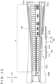
- Figs. 11A to Fig. 13 are diagrams illustrating an example of such a stand. A description will be given below with focus on differences between a stand 101 illustrated in these diagrams and the stand 1 described above. Matters that are not described regarding the stand 101 may be similar to those of the stand 1.
- the stand 101 has the stand main body B and an arm 127.
- the arm 127 extends from the stand main body B toward an outer edge of a lower exterior panel 192B.
- Engagement sections 127A and 127B are formed on the arm 127.
- the engagement sections 127A and 127B engage with an exterior member of an electronic device 190.
- the arm 127 extends toward a back edge 192a of the lower exterior panel 192B as in the stand 1 described above, and the engagement sections 127A and 127B engage with the back edge 92a of the lower exterior panel 92B.
- the stand 101 has an upper member 110 and a lower member 120 that are assembled together in the up-down direction.
- a first supporting surface 111a and a second supporting surface 111b are formed on an upper surface of the upper member 10.
- the lower exterior panel 192B of the electronic device 190 to which the stand 101 is mounted is curved in a manner different from that of the lower exterior panel 92B of the electronic device 90 and is, for example, less undulated than the lower exterior panel 92B.
- the upper member 110 has no mobile stage that can move up and down. Heights of the two supporting surfaces 111a and 111b may be substantially the same.
- the supporting surfaces 111a and 111b may be curved to suit a lower surface of the lower exterior panel 192B.
- Anti-slip members may be provided on the supporting surfaces 111a and 111b.
- the stand main body B (upper member 110) has auxiliary supporting surfaces 112a around the supporting surfaces 111a and 111b.
- the supporting surfaces 111a and 111b are located between the two auxiliary supporting surfaces 112a.
- the auxiliary supporting surfaces 112a may also be curved to suit the lower surface of the lower exterior panel 192B.
- the upper member 110 and the lower member 120 are rotatable relative to each other and are selectively arranged at the horizontal supporting positions and the vertical supporting positions. Assuming that a direction in which the engagement sections 127A and 127B are located with respect to the center of the stand main body B is backward when the upper member 110 and the lower member 120 are at the horizontal supporting positions as illustrated in Fig. 11A , the first supporting surface 111a and the second supporting surface 111b are arranged side by side in the left-right direction. As a result, the first supporting surface 111a and the second supporting surface 111b come in contact with the lower surface of the lower exterior panel 92B as illustrated in Fig. 12 , which makes it possible for the engagement sections 27A and 27B to engage with the back edge 92a of the lower exterior panel 92B.
- the first supporting surface 111a and the second supporting surface 111b are arranged side by side in the front-back direction.
- the electronic device 190 is arranged between the first and second supporting surfaces 111a and 111b of the upper member 10, which makes it possible to arrange the engagement sections 127A and 127B on the back side of the electronic device 190.
- the engagement sections 127A and 127B may be arranged at recessed portions 191m and 191n (refer to Fig. 13 ), respectively, that are formed in a back surface of the electronic device 190.
- the stand 101 may be fastened to the electronic device 190 in the vertical posture by the fixture 31 as with the stand 1.
- the stands 1 and 101 are stands for supporting the electronic devices 90 and 190 having the lower exterior panels 92B and 192B with curved lower surfaces.
- the stands 1 and 101 have the stand main bodies B.
- the stand main bodies B are located, in plan view, inside the outer circumferential edges of the lower exterior panels 92B and 192B and have the supporting surfaces 11a and 11b and the supporting surfaces 111a and 111c to be brought into contact with the lower surfaces.
- the arms 27 and 127 of the stands 1 and 101 extend from the stand main bodies B toward the outer edges of the lower exterior panel 92B of the electronic device 1 and 101 and have the engagement sections 27A and 27B and the engagement sections 127A and 127B ( Fig. 3 , Fig. 4 , Fig.
- the stand main bodies B are located inside the outer circumferential edges of the lower exterior panels 92B and 192B, it is possible to prevent the stand main bodies B from standing out and improve the appearances of the electronic devices 90 and 190 when the electronic devices 90 and 190 is arranged in the horizontal posture. Also, because the arms 27 and 127 extend toward the outer edges of the lower exterior panels 92B and 192B, it is not necessary to provide a structure for fastening the stand main bodies to the curved exterior surfaces (lower surfaces of the lower exterior panels 92B and 192B), which makes it possible to improve the degree of freedom in appearance of the electronic devices.
- the stand proposed in the present disclosure is not limited to the examples of the stands 1 and 101 described above.
- the upper members 10 and 110 and the bottom portions 21 of the lower members 20 and 120 may not be rotatable relative to each other.
- the arms 27 and 127 may be movable relative to the stand main bodies B. Further, the arms 27 and 127 and the mobile stage 13 provided on the upper member 10 may move in a coordinated manner.
Landscapes
- Engineering & Computer Science (AREA)
- General Engineering & Computer Science (AREA)
- Theoretical Computer Science (AREA)
- Mechanical Engineering (AREA)
- Computer Hardware Design (AREA)
- Human Computer Interaction (AREA)
- Physics & Mathematics (AREA)
- General Physics & Mathematics (AREA)
- Multimedia (AREA)
- Microelectronics & Electronic Packaging (AREA)
- Power Engineering (AREA)
- Casings For Electric Apparatus (AREA)
Priority Applications (1)
| Application Number | Priority Date | Filing Date | Title |
|---|---|---|---|
| EP25226501.2A EP4697138A3 (de) | 2020-05-15 | 2021-05-11 | Ständer für elektronische vorrichtung und elektronische vorrichtungsanordnung |
Applications Claiming Priority (2)
| Application Number | Priority Date | Filing Date | Title |
|---|---|---|---|
| JP2020086210 | 2020-05-15 | ||
| PCT/JP2021/017927 WO2021230246A1 (ja) | 2020-05-15 | 2021-05-11 | 電子機器のスタンド、及び電子機器組立体 |
Related Child Applications (1)
| Application Number | Title | Priority Date | Filing Date |
|---|---|---|---|
| EP25226501.2A Division EP4697138A3 (de) | 2020-05-15 | 2021-05-11 | Ständer für elektronische vorrichtung und elektronische vorrichtungsanordnung |
Publications (3)
| Publication Number | Publication Date |
|---|---|
| EP4152902A1 true EP4152902A1 (de) | 2023-03-22 |
| EP4152902A4 EP4152902A4 (de) | 2024-06-12 |
| EP4152902B1 EP4152902B1 (de) | 2025-12-24 |
Family
ID=78524419
Family Applications (2)
| Application Number | Title | Priority Date | Filing Date |
|---|---|---|---|
| EP21803020.3A Active EP4152902B1 (de) | 2020-05-15 | 2021-05-11 | Ständer für elektronische vorrichtung und elektronische vorrichtungsanordnung |
| EP25226501.2A Pending EP4697138A3 (de) | 2020-05-15 | 2021-05-11 | Ständer für elektronische vorrichtung und elektronische vorrichtungsanordnung |
Family Applications After (1)
| Application Number | Title | Priority Date | Filing Date |
|---|---|---|---|
| EP25226501.2A Pending EP4697138A3 (de) | 2020-05-15 | 2021-05-11 | Ständer für elektronische vorrichtung und elektronische vorrichtungsanordnung |
Country Status (5)
| Country | Link |
|---|---|
| US (1) | US12234942B2 (de) |
| EP (2) | EP4152902B1 (de) |
| JP (1) | JP7425190B2 (de) |
| CN (1) | CN115316049B (de) |
| WO (1) | WO2021230246A1 (de) |
Families Citing this family (4)
| Publication number | Priority date | Publication date | Assignee | Title |
|---|---|---|---|---|
| JP2024030267A (ja) * | 2022-08-24 | 2024-03-07 | 株式会社バッファロー | 電子機器及びスタンド |
| JPWO2024176920A1 (de) * | 2023-02-21 | 2024-08-29 | ||
| JP1762180S (ja) * | 2023-06-07 | 2024-01-24 | 電子機器用スタンド | |
| JP1762181S (ja) * | 2023-06-07 | 2024-01-24 | 電子機器用スタンド |
Family Cites Families (15)
| Publication number | Priority date | Publication date | Assignee | Title |
|---|---|---|---|---|
| JP2003134209A (ja) | 2001-10-26 | 2003-05-09 | Toshiba Corp | 無線機器ホルダ |
| WO2004104803A2 (en) * | 2003-05-15 | 2004-12-02 | Hotwire Development, Llc | Universal portable computer stand and high speed connectivity center |
| JP2008228826A (ja) | 2007-03-16 | 2008-10-02 | Pioneer Electronic Corp | 転倒防止装置 |
| JP2009059791A (ja) | 2007-08-30 | 2009-03-19 | Mitsumi Electric Co Ltd | 電子装置 |
| US20090179131A1 (en) * | 2008-01-15 | 2009-07-16 | Charles Lord | Laptop cooling stand with fan |
| CN202452046U (zh) | 2012-01-09 | 2012-09-26 | 讯凯国际股份有限公司 | 携带式电子装置的支撑座 |
| RU2593683C2 (ru) | 2012-04-13 | 2016-08-10 | Сони Компьютер Энтертейнмент Инк. | Электронное устройство |
| US8926414B1 (en) * | 2013-03-15 | 2015-01-06 | Chad Kirkpatrick | Apparatus for supporting and cooling an electronic device |
| JP5801848B2 (ja) | 2013-06-07 | 2015-10-28 | 株式会社ソニー・コンピュータエンタテインメント | 電子機器用スタンド |
| US10813451B2 (en) * | 2014-04-08 | 2020-10-27 | Hypnap LLC | Mobile device stand |
| EP3229642A1 (de) * | 2014-12-10 | 2017-10-18 | FLB Group Limited | Tablet-computer mit abnehmbarem ständer |
| KR200483203Y1 (ko) * | 2015-11-06 | 2017-04-14 | 주식회사 슈피겐코리아 | 모바일 기기용 액세서리 |
| CN210053443U (zh) | 2019-09-06 | 2020-02-11 | 汕头市源盛通塑胶制品有限公司 | 一种手机支架 |
| US20210191461A1 (en) * | 2019-12-23 | 2021-06-24 | Advanced Micro Devices, Inc. | External cooling module |
| US11626686B2 (en) * | 2021-06-14 | 2023-04-11 | Havis, Inc. | Tablet docking station |
-
2021
- 2021-05-11 WO PCT/JP2021/017927 patent/WO2021230246A1/ja not_active Ceased
- 2021-05-11 CN CN202180023431.8A patent/CN115316049B/zh active Active
- 2021-05-11 US US17/998,071 patent/US12234942B2/en active Active
- 2021-05-11 EP EP21803020.3A patent/EP4152902B1/de active Active
- 2021-05-11 JP JP2022521934A patent/JP7425190B2/ja active Active
- 2021-05-11 EP EP25226501.2A patent/EP4697138A3/de active Pending
Also Published As
| Publication number | Publication date |
|---|---|
| US20230175640A1 (en) | 2023-06-08 |
| CN115316049B (zh) | 2026-01-09 |
| EP4697138A2 (de) | 2026-02-18 |
| EP4152902B1 (de) | 2025-12-24 |
| EP4697138A3 (de) | 2026-03-04 |
| US12234942B2 (en) | 2025-02-25 |
| CN115316049A (zh) | 2022-11-08 |
| EP4152902A4 (de) | 2024-06-12 |
| JP7425190B2 (ja) | 2024-01-30 |
| JPWO2021230246A1 (de) | 2021-11-18 |
| WO2021230246A1 (ja) | 2021-11-18 |
Similar Documents
| Publication | Publication Date | Title |
|---|---|---|
| EP4152902B1 (de) | Ständer für elektronische vorrichtung und elektronische vorrichtungsanordnung | |
| KR101057838B1 (ko) | 인터페이싱 부분들을 결합하기 위한 시스템 | |
| US7281936B2 (en) | Modular electronic storage unit | |
| JP6474763B2 (ja) | 電子機器 | |
| KR20190026011A (ko) | 커넥터 | |
| JP2013062377A (ja) | 電気装置 | |
| US20130003286A1 (en) | Portable electronic device | |
| JP6101664B2 (ja) | コネクタ装置 | |
| JP5841669B2 (ja) | カメラ、カメラアッセンブリ及びスタンド部材 | |
| CN108008844A (zh) | 输入设备和包括输入设备的显示设备 | |
| US20080188118A1 (en) | Cover assembly with electronic connectors | |
| KR102824714B1 (ko) | 전자 장치용 거치 장치 | |
| US20130112454A1 (en) | Electronic device housing | |
| US20110220766A1 (en) | Device support structure | |
| TWI850993B (zh) | 浮動連接器 | |
| US20180261958A1 (en) | Connector and connector assembly | |
| WO2024060619A1 (zh) | 电器盒及天井机 | |
| CN113669605B (zh) | 壁挂设备 | |
| CN215344038U (zh) | 充电座组合 | |
| EP4697129A1 (de) | Ständervorrichtung | |
| JP7820567B2 (ja) | 光ディスクドライブ、電子機器ユニット | |
| JP6666574B1 (ja) | 電子機器 | |
| JP2023115938A (ja) | コネクタアッセンブリ | |
| JP4531011B2 (ja) | 卓上電子機器 | |
| GB2478310A (en) | Connector cover for audio/video device |
Legal Events
| Date | Code | Title | Description |
|---|---|---|---|
| STAA | Information on the status of an ep patent application or granted ep patent |
Free format text: STATUS: THE INTERNATIONAL PUBLICATION HAS BEEN MADE |
|
| PUAI | Public reference made under article 153(3) epc to a published international application that has entered the european phase |
Free format text: ORIGINAL CODE: 0009012 |
|
| STAA | Information on the status of an ep patent application or granted ep patent |
Free format text: STATUS: REQUEST FOR EXAMINATION WAS MADE |
|
| 17P | Request for examination filed |
Effective date: 20221113 |
|
| AK | Designated contracting states |
Kind code of ref document: A1 Designated state(s): AL AT BE BG CH CY CZ DE DK EE ES FI FR GB GR HR HU IE IS IT LI LT LU LV MC MK MT NL NO PL PT RO RS SE SI SK SM TR |
|
| DAV | Request for validation of the european patent (deleted) | ||
| DAX | Request for extension of the european patent (deleted) | ||
| A4 | Supplementary search report drawn up and despatched |
Effective date: 20240514 |
|
| RIC1 | Information provided on ipc code assigned before grant |
Ipc: G06F 1/18 20060101ALI20240507BHEP Ipc: A63F 13/90 20140101ALI20240507BHEP Ipc: F16M 11/04 20060101ALI20240507BHEP Ipc: G06F 1/16 20060101ALI20240507BHEP Ipc: H05K 5/02 20060101AFI20240507BHEP |
|
| GRAP | Despatch of communication of intention to grant a patent |
Free format text: ORIGINAL CODE: EPIDOSNIGR1 |
|
| STAA | Information on the status of an ep patent application or granted ep patent |
Free format text: STATUS: GRANT OF PATENT IS INTENDED |
|
| INTG | Intention to grant announced |
Effective date: 20250731 |
|
| GRAS | Grant fee paid |
Free format text: ORIGINAL CODE: EPIDOSNIGR3 |
|
| GRAA | (expected) grant |
Free format text: ORIGINAL CODE: 0009210 |
|
| STAA | Information on the status of an ep patent application or granted ep patent |
Free format text: STATUS: THE PATENT HAS BEEN GRANTED |
|
| AK | Designated contracting states |
Kind code of ref document: B1 Designated state(s): AL AT BE BG CH CY CZ DE DK EE ES FI FR GB GR HR HU IE IS IT LI LT LU LV MC MK MT NL NO PL PT RO RS SE SI SK SM TR |
|
| P01 | Opt-out of the competence of the unified patent court (upc) registered |
Free format text: CASE NUMBER: UPC_APP_0013251_4152902/2025 Effective date: 20251113 |
|
| REG | Reference to a national code |
Ref country code: CH Ref legal event code: F10 Free format text: ST27 STATUS EVENT CODE: U-0-0-F10-F00 (AS PROVIDED BY THE NATIONAL OFFICE) Effective date: 20251224 Ref country code: GB Ref legal event code: FG4D |
|
| REG | Reference to a national code |
Ref country code: DE Ref legal event code: R096 Ref document number: 602021045082 Country of ref document: DE |
|
| REG | Reference to a national code |
Ref country code: NL Ref legal event code: FP |
|
| REG | Reference to a national code |
Ref country code: LT Ref legal event code: MG9D |
|
| PG25 | Lapsed in a contracting state [announced via postgrant information from national office to epo] |
Ref country code: NO Free format text: LAPSE BECAUSE OF FAILURE TO SUBMIT A TRANSLATION OF THE DESCRIPTION OR TO PAY THE FEE WITHIN THE PRESCRIBED TIME-LIMIT Effective date: 20260324 |
|
| PG25 | Lapsed in a contracting state [announced via postgrant information from national office to epo] |
Ref country code: FI Free format text: LAPSE BECAUSE OF FAILURE TO SUBMIT A TRANSLATION OF THE DESCRIPTION OR TO PAY THE FEE WITHIN THE PRESCRIBED TIME-LIMIT Effective date: 20251224 Ref country code: HR Free format text: LAPSE BECAUSE OF FAILURE TO SUBMIT A TRANSLATION OF THE DESCRIPTION OR TO PAY THE FEE WITHIN THE PRESCRIBED TIME-LIMIT Effective date: 20251224 |
|
| PG25 | Lapsed in a contracting state [announced via postgrant information from national office to epo] |
Ref country code: RS Free format text: LAPSE BECAUSE OF FAILURE TO SUBMIT A TRANSLATION OF THE DESCRIPTION OR TO PAY THE FEE WITHIN THE PRESCRIBED TIME-LIMIT Effective date: 20260324 |
|
| PG25 | Lapsed in a contracting state [announced via postgrant information from national office to epo] |
Ref country code: LV Free format text: LAPSE BECAUSE OF FAILURE TO SUBMIT A TRANSLATION OF THE DESCRIPTION OR TO PAY THE FEE WITHIN THE PRESCRIBED TIME-LIMIT Effective date: 20251224 |
|
| PG25 | Lapsed in a contracting state [announced via postgrant information from national office to epo] |
Ref country code: BG Free format text: LAPSE BECAUSE OF FAILURE TO SUBMIT A TRANSLATION OF THE DESCRIPTION OR TO PAY THE FEE WITHIN THE PRESCRIBED TIME-LIMIT Effective date: 20251224 |