EP4137954B1 - Verarbeitungssystem, zugehörige integrierte schaltung, vorrichtung und verfahren - Google Patents
Verarbeitungssystem, zugehörige integrierte schaltung, vorrichtung und verfahren Download PDFInfo
- Publication number
- EP4137954B1 EP4137954B1 EP22188131.1A EP22188131A EP4137954B1 EP 4137954 B1 EP4137954 B1 EP 4137954B1 EP 22188131 A EP22188131 A EP 22188131A EP 4137954 B1 EP4137954 B1 EP 4137954B1
- Authority
- EP
- European Patent Office
- Prior art keywords
- reception
- signal
- transmission
- data
- shift register
- Prior art date
- Legal status (The legal status is an assumption and is not a legal conclusion. Google has not performed a legal analysis and makes no representation as to the accuracy of the status listed.)
- Active
Links
Images


Classifications
-
- G—PHYSICS
- G06—COMPUTING OR CALCULATING; COUNTING
- G06F—ELECTRIC DIGITAL DATA PROCESSING
- G06F13/00—Interconnection of, or transfer of information or other signals between, memories, input/output devices or central processing units
- G06F13/38—Information transfer, e.g. on bus
- G06F13/40—Bus structure
- G06F13/4063—Device-to-bus coupling
- G06F13/4068—Electrical coupling
- G06F13/4072—Drivers or receivers
-
- H—ELECTRICITY
- H04—ELECTRIC COMMUNICATION TECHNIQUE
- H04L—TRANSMISSION OF DIGITAL INFORMATION, e.g. TELEGRAPHIC COMMUNICATION
- H04L12/00—Data switching networks
- H04L12/28—Data switching networks characterised by path configuration, e.g. LAN [Local Area Networks] or WAN [Wide Area Networks]
- H04L12/40—Bus networks
- H04L12/40006—Architecture of a communication node
- H04L12/40013—Details regarding a bus controller
-
- G—PHYSICS
- G06—COMPUTING OR CALCULATING; COUNTING
- G06F—ELECTRIC DIGITAL DATA PROCESSING
- G06F13/00—Interconnection of, or transfer of information or other signals between, memories, input/output devices or central processing units
- G06F13/14—Handling requests for interconnection or transfer
- G06F13/20—Handling requests for interconnection or transfer for access to input/output bus
- G06F13/28—Handling requests for interconnection or transfer for access to input/output bus using burst mode transfer, e.g. direct memory access DMA, cycle steal
-
- G—PHYSICS
- G06—COMPUTING OR CALCULATING; COUNTING
- G06F—ELECTRIC DIGITAL DATA PROCESSING
- G06F13/00—Interconnection of, or transfer of information or other signals between, memories, input/output devices or central processing units
- G06F13/38—Information transfer, e.g. on bus
- G06F13/382—Information transfer, e.g. on bus using universal interface adapter
- G06F13/385—Information transfer, e.g. on bus using universal interface adapter for adaptation of a particular data processing system to different peripheral devices
-
- G—PHYSICS
- G06—COMPUTING OR CALCULATING; COUNTING
- G06F—ELECTRIC DIGITAL DATA PROCESSING
- G06F13/00—Interconnection of, or transfer of information or other signals between, memories, input/output devices or central processing units
- G06F13/38—Information transfer, e.g. on bus
- G06F13/40—Bus structure
- G06F13/4063—Device-to-bus coupling
- G06F13/4068—Electrical coupling
-
- G—PHYSICS
- G06—COMPUTING OR CALCULATING; COUNTING
- G06F—ELECTRIC DIGITAL DATA PROCESSING
- G06F13/00—Interconnection of, or transfer of information or other signals between, memories, input/output devices or central processing units
- G06F13/38—Information transfer, e.g. on bus
- G06F13/42—Bus transfer protocol, e.g. handshake; Synchronisation
- G06F13/4204—Bus transfer protocol, e.g. handshake; Synchronisation on a parallel bus
- G06F13/4221—Bus transfer protocol, e.g. handshake; Synchronisation on a parallel bus being an input/output bus, e.g. ISA bus, EISA bus, PCI bus, SCSI bus
- G06F13/423—Bus transfer protocol, e.g. handshake; Synchronisation on a parallel bus being an input/output bus, e.g. ISA bus, EISA bus, PCI bus, SCSI bus with synchronous protocol
-
- G—PHYSICS
- G06—COMPUTING OR CALCULATING; COUNTING
- G06F—ELECTRIC DIGITAL DATA PROCESSING
- G06F13/00—Interconnection of, or transfer of information or other signals between, memories, input/output devices or central processing units
- G06F13/38—Information transfer, e.g. on bus
- G06F13/42—Bus transfer protocol, e.g. handshake; Synchronisation
- G06F13/4282—Bus transfer protocol, e.g. handshake; Synchronisation on a serial bus, e.g. I2C bus, SPI bus
-
- H—ELECTRICITY
- H04—ELECTRIC COMMUNICATION TECHNIQUE
- H04L—TRANSMISSION OF DIGITAL INFORMATION, e.g. TELEGRAPHIC COMMUNICATION
- H04L12/00—Data switching networks
- H04L12/28—Data switching networks characterised by path configuration, e.g. LAN [Local Area Networks] or WAN [Wide Area Networks]
- H04L12/40—Bus networks
- H04L12/40006—Architecture of a communication node
- H04L12/40032—Details regarding a bus interface enhancer
-
- H—ELECTRICITY
- H04—ELECTRIC COMMUNICATION TECHNIQUE
- H04L—TRANSMISSION OF DIGITAL INFORMATION, e.g. TELEGRAPHIC COMMUNICATION
- H04L12/00—Data switching networks
- H04L12/28—Data switching networks characterised by path configuration, e.g. LAN [Local Area Networks] or WAN [Wide Area Networks]
- H04L12/40—Bus networks
- H04L12/40169—Flexible bus arrangements
-
- H—ELECTRICITY
- H04—ELECTRIC COMMUNICATION TECHNIQUE
- H04L—TRANSMISSION OF DIGITAL INFORMATION, e.g. TELEGRAPHIC COMMUNICATION
- H04L12/00—Data switching networks
- H04L12/28—Data switching networks characterised by path configuration, e.g. LAN [Local Area Networks] or WAN [Wide Area Networks]
- H04L12/40—Bus networks
- H04L2012/40208—Bus networks characterized by the use of a particular bus standard
- H04L2012/40215—Controller Area Network CAN
Definitions
- Embodiments of the present disclosure relate to a microcontroller configured to exchange data via a CAN FD bus.
- FIG. 1 shows a typical electronic system, such as the electronic system of a vehicle, comprising a plurality of processing systems 10, such as embedded systems or integrated circuits, e.g., a Field Programmable Gate Array (FPGA), a Digital Signal Processor (DSP) or a micro-controller (e.g., dedicated to the automotive market).
- processing systems 10 such as embedded systems or integrated circuits, e.g., a Field Programmable Gate Array (FPGA), a Digital Signal Processor (DSP) or a micro-controller (e.g., dedicated to the automotive market).
- FPGA Field Programmable Gate Array
- DSP Digital Signal Processor
- micro-controller e.g., dedicated to the automotive market.
- the communication system may include a vehicle control bus, such as a Controller Area Network (CAN) bus, and possibly a multimedia bus, such as a Media Oriented Systems Transport (MOST) bus, connected to vehicle control bus via a gateway.
- vehicle control bus such as a Controller Area Network (CAN) bus
- multimedia bus such as a Media Oriented Systems Transport (MOST) bus
- the processing systems 10 are located at different positions of the vehicle and may include, e.g., an Engine Control Unit, a Transmission Control Unit (TCU), an Anti-lock Braking System (ABS), a Body Control Module (BCM), and/or a navigation and/or multimedia audio system.
- TCU Transmission Control Unit
- ABS Anti-lock Braking System
- BCM Body Control Module
- one or more of the processing systems 10 may also implement real-time control and regulation functions.
- These processing systems are usually identified as Electronic Control Units.
- FIG 2 shows a block diagram of an exemplary digital processing system 10, in particular a microcontroller, which may be used as any of the processing systems 10 of Figure 1 .
- the processing system 10 comprises a microprocessor 102, usually the Central Processing Unit (CPU), programmed via software instructions.
- the software executed by the microprocessor 102 is stored in a non-volatile program memory 104, such as a Flash memory or EEPROM.
- the memory 104 is configured to store the firmware of the processing unit 102, wherein the firmware includes the software instructions to be executed by the microprocessor 102.
- the non-volatile memory 104 may also be used to store other data, such as configuration data, e.g., calibration data.
- the microprocessor 102 usually has associated also a volatile memory 104b, such as a Random-Access-Memory (RAM).
- a volatile memory 104b such as a Random-Access-Memory (RAM).
- RAM Random-Access-Memory
- the memory 104b may be used to store temporary data.
- the communication with the memories 104 and/or 104b is performed via one or more memory controllers 100.
- the memory controller(s) 100 may be integrated in the microprocessor 102 or connected to the microprocessor 102 via a communication channel, such as a system bus of the processing system 10.
- the system bus may comprise one or more bus systems, e.g., based on the Advanced extensible Interface (AXI) bus architecture, and/or a Network-on-Chip (NoC).
- AXI Advanced extensible Interface
- NoC Network-on-Chip
- the memories 104 and/or 104b may be integrated with the microprocessor 102 in a single integrated circuit, or the memories 104 and/or 104b may be in the form of a separate integrated circuit and connected to the microprocessor 102, e.g., via the traces of a printed circuit board.
- the microprocessor 102 may have associated one or more (hardware) resources/peripherals 106 selected from the group of
- a dedicated digital components DC may also correspond to a FPGA integrated in the processing system 10.
- the memory 104 may also comprise the program data for such a FPGA.
- the system bus may indeed comprise an Advanced Microcontroller Bus Architecture (AMBA) High-performance Bus (AHB), and an Advanced Peripheral Bus (APB) used to connect the resources/peripherals 106 to the AMBA AHB bus.
- AMBA Advanced Microcontroller Bus Architecture
- AHB Advanced Peripheral Bus
- the digital processing system 10 may support different functionalities.
- the behavior of the microprocessor 102 is determined by the firmware stored in the memory 104, e.g., the software instructions to be executed by a microprocessor 102 of a micro-controller 10.
- the firmware stored in the memory 104
- CAN FD Light protocol is described in documents " CAN FD Light Specification and test plan", CAN in Automation (CiA) 604-1, version 0.0.6, or " CAN FD Light Network Protocol and Implementation", EuES003-06, version 1.3.
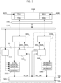
- Figure 3 shows a typical situation, where a first processing system 10 1 and a second processing system 10 2 are connected to a CAN FD Light bus 20.
- each of the processing systems 10 1 and 10 2 may comprise:
- CAN bus transceivers 320 are usually required, because the CAN bus 20 uses different signal levels than the processing unit 102 and/or in order to implement a galvanic isolation.
- the transceivers 320 are Controller Area Network Flexible Data-Rate (CAN FD) transceivers.
- CAN FD Controller Area Network Flexible Data-Rate
- conventional CAN bus transceivers 320 comprises two interfaces.
- the first interface is configured to exchange data via the CAN bus 20 by transmitting and receiving differential non-return-to-zero (NRZ) encoded signals.
- the second interface is configured to receive a transmission signal Tx and provide a reception signal Rx, wherein the transmission signal Tx and the reception signal Rx are NRZ signals, preferably unipolar non-return-to-zero level (NRZ-L) encoded signals, such as binary-encoded signals being set to high (typically the supply voltage of the processing unit 102) for transmitting a logic "1" or low (typically ground) for transmitting a logic "0".
- NRZ-L unipolar non-return-to-zero level
- the communication interface IF may provide the NRZ/binary encoded transmission signal TX to the transceiver 320 and receive the NRZ/binary encoded reception signal RX from the transceiver 320.
- the transceiver 320 manages the data exchange on the CAN bus 20.
- the communication interface IF implements (at least) the data link layer and optional further higher protocol layers, while the transceivers 320 manages the physical layer.
- the interface IF may implement a CAN FD Light controller.
- the transceivers 320 may be provided in the form of a separate integrated circuit 32 connected to an integrated circuit 30 comprising the processing unit 102, and the hardware interface IF (see, e.g., processing system 10 1 ), or the transceivers 320 may be integrated in the integrated circuit 30 comprising the processing unit 102, and the hardware interface IF (see, e.g., processing system 10 2 ).
- the CAN FD Light controller IF may also be integrated in the integrated circuit 32 of the transceiver 320.
- the present application relates to a processing system configured to manage a CAN FD Light data transmission mode and/or CAN FD Light data reception mode.
- AN5086 " I2S protocol emulation on STM32L0 Series microcontrollers using a standard SPI peripheral", 11 December 2017, XP055917581 , and documents US 2010/146157 A1 and US 2016/344552 A1 may be of interest for the present application.
- the above objective is achieved by means of a processing system having the features specifically set forth in the claims that follow.
- Embodiments moreover concern a related integrated circuit, device and method.
- various embodiments relate to a processing system, such as an integrated circuit, e.g., a micro-controller, adapted to transmit and receive CAN FD Light frames.
- the processing system is configured to transmit and receive CAN FD Light frames via a Serial Peripheral Interface, SPI, communication interface.
- SPI Serial Peripheral Interface
- the processing system comprises a transmission terminal configured to provide a transmission signal, a reception terminal configured to receive a reception signal and a clock terminal.
- the SPI communication interface is connected to the transmission terminal and the reception terminal, and comprises a control register configured to store data identifying a clock scaling factor and data identifying a mode of operation, wherein the mode of operation indicates a master mode or a slave mode.
- the SPI communication interface may comprise a transmission shift register of a given word size configured to generate the transmission signal by sequentially providing the content of the transmission shift register in response to a first clock signal, a reception shift register of the given word size configured to sequentially add the logic level of the reception signal to the content of the reception shift register in response to a second clock signal, and a clock downscale circuit configured to receive a clock signal and generate a downscaled clock signal by downscaling the clock signal as a function of the clock scaling factor.
- the SPI communication interface may provide the downscaled clock signal as the first clock signal to the transmission shift register.
- the downscaled clock signal is also provided as the second clock signal to the reception shift register.
- the SPI communication interface may provide a clock signal received at the clock terminal as the second clock signal to the reception shift register.
- the clock signal received at the clock terminal is also provided as the first clock signal to the transmission shift register.
- the processing system comprises also a microprocessor programmable via software instructions, a memory controller configured to be connected to a memory and a communication system connecting the microprocessor, the memory controller and the SPI communication interface.
- the processing system is configured to transmit and receive CAN FD Light frames via the SPI communication interface.
- the transmission terminal and the reception terminal should be connected to a CAN FD transceiver.
- the processing system comprises a first DMA channel configured to transfer packets of the given word size from the memory to the transmission shift register and a second DMA channel configured to transfer packets of the given word size from the reception shift register to the memory.
- the processing system comprises the following additional blocks for receiving a CAN FD Light frame:
- the edge detector is used to detect the start of a new CAN FD Light frame
- the first hardware timer circuit is used to generate the clock signal for the SPI communication interface
- the second hardware timer circuit is used to detect the end of the CAN FD Light frame.
- the counter of the second hardware timer circuit is configure to, when enabled, assert the second control signal in response to determining that the reception signal is set to high for a given time threshold, wherein the time threshold corresponds at least to the duration of eight clock cycles of the clock signal generated by the first hardware timer circuit, and wherein the counter of the second hardware timer circuit is configured to be reset in response to detecting that the reception signal is low. Accordingly, in this case, the second counter detects the presence of eight consecutive bits being set to high, which corresponds to the end-of-frame indication of a CAN FD Light frame.
- the given threshold value of the second hardware timer circuit corresponds at least to the duration of a given maximum number of clock cycles of the clock signal generated by the first hardware timer circuit. Accordingly, in this case, the second counter signals that a given maximum number of bits have been received.
- the first hardware timer circuit and/or the second hardware timer circuit may be general purpose hardware timer circuits.
- the first hardware timer circuit implements a Pulse Width Modulation (PWM) signal generator.
- the first hardware timer circuit may comprise a counter configure to, when enabled, to generate the clock signal as a PWM signal.
- the processing system may manage a CAN FD Light data transmission mode and/or CAN FD Light data reception mode,
- the microprocessor may be configured to program the control register of the SPI communication interface in order to activate the master mode, generate a transmission CAN FD Light frame, store the transmission CAN FD Light frame to the memory, and activate the first DMA channel, whereby the first DMA channel sequentially transfers the transmission CAN FD Light frame from the memory to the transmission shift register and the SPI communication interface transmits the respective data stored to the transmission shift register.
- the microprocessor may be configured to program the control register of the SPI communication interface in order to activate the slave mode, and then wait that the first control signal, such as an interrupt signal, is asserted by the first timer circuit, thus indicating the start of a reception CAN FD Light frame.
- the microprocessor may then enable the first hardware timer circuit and the second hardware timer circuit, whereby the second DMA channel is configured to transfer packets of the given word size from the reception shift register to the memory, thereby sequentially transferring the reception CAN FD Light frame from the reception shift register to the memory.
- the microprocessor then waits that the second control signal, such as an interrupt signal, is asserted by the second timer circuit, thus indicating the end of the reception CAN FD Light frame. Accordingly, in response to the second control signal, the microprocessor may read the reception CAN FD Light frame from the memory. In various embodiments, in response to the second control signal, the microprocessor may also disable the first hardware timer circuit and the second hardware timer circuit.
- the second control signal such as an interrupt signal
- the clock signal generated by the first hardware timer circuit may also be synchronized with the reception signal.
- the counter of the first hardware timer circuit may be configured to be reset in response to detecting a falling and/or rising edge of the reception signal, as signaled, e.g., by the edge detector or a further edge detector.
- the processing system may implement both a CAN FD Light controller/master or a CAN FD Light slave.
- a CAN FD Light controller/master first transmits a transmission CAN FD Light frame and then optionally receives a reception CAN FD Light frame.
- a CAN FD Light slave first receives a reception CAN FD Light frame and then optionally transmits a transmission CAN FD Light frame.
- FIG. 4 shows an embodiment of a processing system 10a in accordance with the present description.
- the processing system 10a comprises at least one processing core 102a, such as n processing cores 102a 1 ...102a n , connected to a (on-chip) communication system 114.
- the processing cores 102a 1 ...102a n may be ARM Cortex ® -R52 cores.
- the communication system 114 may comprise one or more bus systems, e.g., based on the Advanced extensible Interface (AXI) bus architecture, and/or a Network-on-Chip (NoC).
- AXI Advanced extensible Interface
- NoC Network-on-Chip
- each processing core 102a may comprise a microprocessor 1020 and a communication interface 1022 configured to manage the communication between the microprocessor 1020 and the communication system 114.
- the interface 1022 is a master interface configured to forward a (read or write) request from the microprocessor 1020 to the communication system 114, and forward an optional response from the communication system 114 to the microprocessor 1020.
- the processing core 102a may also comprise a slave interface 1024.
- a first microprocessor 1020 may send a request to a second microprocessor 1020 (via the communication interface 1022 of the first microprocessor, the communication system 114 and the communication interface 1024 of the second microprocessor).
- the communication system 114 may comprise in addition to a system bus or NoC, also an additional co-processor bus, e.g., connecting the microprocessors 1020 of the same processing core 102a or all processing cores 102a.
- each processing core 102a 1 ...102a n may also comprise further local resources, such as one or more local memories 1026, usually identified as Tightly Coupled Memory (TCM).
- TCM Tightly Coupled Memory
- the processing cores 102a 1 ...102a n are arranged to exchange data with a non-volatile memory 104 and/or a volatile memory 104b.
- these memories are system memories, i.e., shared for the processing cores 102a 1 ...102a n .
- the processing system 10a comprises one or more memory controllers 100 configured to connect at least one non-volatile memory 104 and at least one volatile memory 104b to the communication system 114.
- one or more of the memories 104 and/or 104b may be integrated in an integrated circuit 30a comprising the processing core(s) 102a or may be connected externally to the integrated circuit 30a.
- the processing system 10a may comprise:
- the processing system 10a may comprise one or more resources 106, such as one or more communication interfaces or co-processors (e.g ., a cryptographic co-processor).
- resources 106 such as one or more communication interfaces or co-processors (e.g ., a cryptographic co-processor).
- the processing system 10a comprises a communication interface 50 connected to the communication system 114 via a slave communication interface 510.
- the communication interface 50 comprises:
- the same registers may be used as transmission data registers DATATX and reception data registers DATARX.
- a processing core 102a may be configured to send one or more of the following requests via the communication system 114 to the slave interface 510 of the communication interface 50:
- a processing core 102a may write a given number k of data packets TD1..TDk to the m transmission data registers DATATX, or read a given number k of data packets RD 1. RDk from the m reception data registers DATARX.
- the number k of data packets may correspond to or be smaller than the number m of registers.
- each of the registers DATATX, DATARX and CTRL may have associated a respective physical address (PA) of the communication system 114, and each read or write request may comprise a given target address.
- the communication system 114 may comprise an Advanced Microcontroller Bus Architecture (AMBA) High-performance Bus (AHB), and an Advanced Peripheral Bus (APB) used to connect the communication interface 50 to the AMBA AHB bus.
- AMBA Advanced Microcontroller Bus Architecture
- AHB Advanced Peripheral Bus
- the processing system 10a comprises also one or more Direct-Memory-Access (DMA) controllers 110.
- DMA controller 110 comprises at least one functional channel connected to a resource 106.
- the communication interface 50 may be connected to the DMA controller 110 via two channels:
- the communication interface 50 comprises two DMA interface circuits 506 1 and 506 2 .
- the first DMA interface circuit 506 1 is connected to the DMA channel DMA 1 and generates a first request signal REQ 1 used to request new data to be transmitted.
- the second DMA interface circuit 506 2 is connected to the DMA channel DMA 2 and generates a second request signal REQz used to request the reading of the received data.
- the DMA channel DMA 1 and/or the DMA channel DMA 2 may be implemented with a general-purpose DMA controller, or via an integrated DMA controller, which may be configured to send read or write requests, respectively, either to the communication system 114 or directly the memory controller 110.
- the DMA channel DMA 1 is implemented with a general-purpose DMA channel, which thus transfers data to the registers DATATX via the slave interface 510
- the DMA channel DMA 2 is an integrated DMA write channel implemented in the communication interface 50, which thus transfers data directly from the registers DATARX either to the communication system 114 or directly to the memory controller 100.
- a data transmission may be started by writing the content of the control register(s) CTRL, e.g., in order to set a flag enabling the data transmission and/or a flag enabling DMA transfer.
- the DMA interface circuit 506 1 may assert the request signal REQ 1 , whereby the DMA channel DMA 1 transfers a given number k of data packets TDL.TDk from the memory 104b to the m transmission data registers DATATX.
- the source address of the DMA channel DMA 1 may be initialized to the address ADR 1 of the first memory slot TD1 used to store the transmission data and may be increased for each DMA data transfer.
- the target address may be initialized to the address associated with the first transmission data register DATATX0 and the target address may be increased for each DMA data transfer.
- the DMA channel DMA 1 may also assert an acknowledge signal ACK 1 indicating that the requested number k of packets TD1..TDk has been transferred to the transmission data registers DATATX.
- the DMA interface circuit 506 1 may de-assertthe request signal REQ 1 in response to the acknowledge signal ACK 1 .
- the hardware communication interface 504 may start the data transmission in response to the acknowledge signal ACK 1 .
- the hardware communication interface 504 may assert a signal TX_OK.
- the DMA interface circuit 506 1 may assert again the request signal REQ 1 , thereby requesting new data.
- the signal TX_OK may be used to generate an interrupt for a processing core 102a.
- the hardware communication interface 504 may assert a signal RX_OK.
- the DMA interface circuit 506 2 may be configured to assert the request signal REQ 2
- the DMA channel DMA 2 may be configured to transfer k packets from the m reception data registers DATARX to the memory 104b, thereby sequentially storing the received data RD 1..RDn to the memory 104b.
- the source address of the DMA channel DMA 2 may be initialized to the address associated with the first reception data register DATARX0 and the source address is increased for each data transfer.
- the target address may be initialized to the address ADR 2 of the first memory slot RD 1 used to store the received data and may be increased for each data transfer.
- the DMA channel DMA 2 may also assert an acknowledge signal ACK 2 indicating that the requested number k of packets RD1..RDk has been transferred to the memory 104b.
- the DMA interface circuit 506 2 may de-assert the request signal REQ 2 in response to the acknowledge signal ACK 2 .
- the DMA interface circuit 506 2 may assert a ready signal RDY, which is provided to the hardware communication interface 504.
- the hardware communication interface 504 may be configured to only accept new data when the signal RDY is asserted.
- the acknowledge signal ACK 2 may be used to generate an interrupt for a processing core 102a.
- the DMA controller 110 may thus comprise:
- the communication interface 50 is a serial communication interface configured to:
- the transmission signal TXD and the reception signal RXD may be connected to a transmission terminal TX and a reception terminal RX, respectively.
- the transmission terminal TX and the reception terminal RX are connected to a CAN FD transceiver 320 in order to exchange data via a CAN FD Light bus 20.
- the transmission terminal TX and the reception terminal RX may be pads of the die of the integrated circuit 30a or pins of a packaged integrated circuit 30a, wherein the CAN FD transceiver 320 is provided in a separate integrated circuit 32.
- the CAN FD transceiver 320 may be integrated in the integrated circuit 30a.
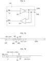
- Figure 6 shows a possible embodiment of a CAN FD transceiver 320.
- the transceiver 320 is configure to receive a NRZ (e.g., NRZ-L) encoded transmission signal TXD, such as a binary bit sequence.
- the transceiver 320 comprises thus a CAN FD transmitter circuit 322, wherein the transmitter circuit 322 is connected to pins/pads CANH and CANL to be connected to the differential data wires of the CAN FD (Light) bus 20.
- the transceiver 320 comprises also a CAN FD receiver circuit 324 configured to generate a signal RXD by analyzing the voltage between the terminals CANH and CANL.
- the signal RXD is a NRZ encoded signals, such as binary encoded signals.
- a CAN transceiver 320 essentially converts the voltage levels of the signals, while the CAN FD Light protocol management and the respective timing of the signals has to be implemented in the CAN FD Light controller implemented in the processing system 10a. Accordingly, in various embodiments, the processing system 10a should be able to generate the transmission signal TXD according to the CAN FD Light protocol, and similarly reconstruct a transmitted bit sequence based on the logic level of the received signal RXD.
- CAN FD Light is a commander/responder protocol based on the CAN FD protocol. This is described in the reference documents cited previously.
- CAN FD protocol Generally, concerning the CAN FD protocol, reference can be made also to documents "Road vehicles - Controller area network (CAN) - Part 1: Data link layer and physical signaling", ISO 11898-1:2015 2015, “Road vehicles - Controller area network (CAN) - Part 2: Highspeed medium access unit", ISO 11898-2:2016 2016, and/or "RM0407 Reference manual - SPC584Cx / SPC58ECx 32-bit MCU family built on the PowerArchitecture for automotive body electronics applications", RM0407 Rev. 5, May/2019
- the commander controls the entire communication and initiates each communication cycle by either sending a frame without expecting an answer from the other network participants ("responders"), such as broadcast frames, or by sending a frame to a dedicated addressed responder while expecting an answer from this responder. i.e., unicast frames in a request and answer scheme.
- the request frames can also be used to send data to the addressed responder. Only the addressed responder from which an answer is requested is expected to send a frame back, i.e., no other device on the bus is expected to send data at the same time. Accordingly, the sequence of frames on the bus 20 is precisely defined and no arbitration is required.
- Figures 7A and 7B show a typical CAN FD Light frame.
- the CAN FD Light protocol uses a dominant logic level, which usually corresponds to the low logic level ("0"), and a recessive logic level, which usually corresponds to the high logic level ("1").
- the implementation of the logic level of the dominant and recessive logic level depends on the implementation of the CAN FD transceiver 320.
- a CAN FD Light frame comprises, as specified in ISO 11898-1:2015, in sequence:
- the CAN controller may thus prepare the complete frame prior to transmission and then send the bit-sequence of the frame without running an arbitration.
- a processing core 102a may prepare the complete CAN FD Light frame represented by the transmission data TD1..TDk, and then either:
- Figure 12 shows in this respect an embodiment of the operation, e.g., implemented via software instructions, of the processing core 102a in order to transmit data.
- the processing core 102a decides to transmit given data via the communication interface 50/the CAN FD Light bus 20, thus starting the generation of the transmission frame/data TD 1..TDk.
- the processing core 102a sets at a step 2004 the start-of-frame bit SOF to the dominant level. As will be described later on, this step is purely optional.
- the processing core 102a obtains a standard identifier at a step 2006 and adds at a step 2004 the respective standard identifier to the field SID of the transmission frame TD 1.. TDk.
- the processing core 102a adds at a step 2008 predefined CAN FD Light control bits to the transmission frame TD 1.
- the control bits include the bits RRS, IDE, FDF, BRS, and ESI, which may have fixed levels for a CAN FD Light frame.
- the processing core 102a obtains at a step 2012 the data to be transmitted, determines at a step 2010 the corresponding data length code (DLC) and adds at a step 2014 the data length code to the field DLC and the data to be transmitted to the field DATA of the transmission frame TD 1..TDk.
- DLC data length code
- the processing core 102a adds then possible stuff bits according to the bit stuff rule of the CAN FD Light standard ISO 11898-1:2015, and calculates at a step 2018 the respective stuff bit count and adds the stuff bit count to the field SBC of the transmission frame TD 1..TDk. Similarly, the processing core 102a may determine the value of the parity bit and add the parity bit to the field P of the transmission frame TD 1.. TDk.
- the processing core 102a determines then the respective number of CRC bits and adds the CRC bits to the field CRC of the transmission frame TD1..TDk.
- fixed stuff bits according to ISO 11898-1:2015 may also be added in this step.
- processing core 102a adds at a step 2022 the trailing bits for the acknowledge fields AS and AD, and the end-of-frame delimiter EOF.
- the processing core 102a may determine at a step 2024 the frame length and store data identifying the frame length to the control register CTRL of the communication interface 50.
- the processing core 102a may store at a step 2026 the transmission frame/data TD1..TDk to the transmission data registers DATATX, or to the memory 104b and activate the DMA transfer of the DMA channel DMA 1 .
- the processing core 102a may activate at a step 2028 the data transmission operation, e.g., by setting a respective bit in the control register CTRL, and the procedure terminates at a step 2030.
- control register CTRL may also be combined by performing only a single programming of the control register CTRL.
- the processing core 102a may monitor a flag in the control register CTRL and/or receive an interrupt from the communication interface 50 (e.g., both set in response to the signal TX_OK).
- Figure 13 shows in this respect an embodiment of the operation, e.g., implemented via software instructions, of the processing core 102a in order to receive data.
- the processing core 102a may read at a step 2042 the received frame/data RD 1..RDk.
- the processing core 102a may monitor a flag in the control register CTRL and/or receive an interrupt from the communication interface 50.
- the flag and/or interrupt may be asserted when the communication interface 50 stores the data to the reception data registers DATARX ( e.g ., as indicated by the signal RX_OK) and/or once having transferred the data RD1..RDk to the memory 104b via the DMA channel DMA 2 ( e.g ., as indicated by the signal ACK 2 ).
- the processing core 102a may read the received frame/data RD 1..RDk form the reception data registers DATARX or the memory 104b. Accordingly, in various embodiments, prior to receiving data, the processing core 102a may activate the DMA transfer of the DMA channel DMAz, whereby the DMA channel DMA 2 transfers the received frame from the reception data registers DATARX to the memory 104b.
- the processing core 102a may then calculate the CRC data for the received frame/data RD 1..RDk, and may compare at a step 2046 the received CRC data (field CRC, e.g., after removal of the fixed stuff bits according ISO 11898-1:2015) with the calculated CRC data.
- the processing core 102a may disregard/drop the received data at a step 2048, and the procedure terminates at a stop step 2056.
- the processing core 102a removes at a step 2050 possible stuff bits.
- the processing core 102a may then obtain the standard identifier SID.
- the processing core 102a may extract the data from the received frame/data RD 1..RDk. Generally, in order to determine the length of the data field DATA (and thus the length of the CRC field), the processing core 102a may extract the data length code DLC and/or may determine the number of bits received. Accordingly, at the step 2054, the processing core 102a has obtained the identifier SID and the respective data DATA, and the procedure terminates at the step 2056.
- the transmission portion of the hardware serial communication interface 504 may be configured to transfer a given number of bits corresponding to the length of the transmission frame stored to the transmission data registers DATATX according to the timing of the CAN FD Light standard.
- the reception portion of the hardware serial communication interface 504 should be configured to receive the reception frame according to the timing of the CAN FD Light standard and store the frame to the reception data registers DATARX.
- the reception portion in order to determine the length of the reception frame, the reception portion should also be configured to detect the End-of-Frame field EOF ⁇ 6:0> having all bits set to the recessive level ( e.g., " 1").
- the reception portion is configured to determine the end of the frame by detecting eight consecutive bits being set to the recessive level.
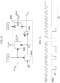
- FIG. 8 shows an embodiment of the hardware serial communication interface 504.
- the hardware communication interface 504 comprises two shift registers 5040 and 5042.
- the shift register 5040 is used to store the data to be transmitted.
- a CAN FD Light frame as shown in Figures 7A and 7B includes a single start-of-frame bit SOF (set to the dominant level) and seven end-of-frame bits EOF (set to the recessive level).
- a CAN FD Light frame may comprise up to 675 bits.
- the CAN FD Light comprises a fixed number of 35 bits comprising 22 bits of control fields SOF, ID, RRS, IDE, FDF, res, BRS, ESI and DLC, 4 bits for the stuff bit counter field SBC and the parity bit P, 2 bits for the acknowledge fields AS and AD, and 7 bits for end-of-frame field EOF.
- a number of variable bits may be added, i.e., the data field DATA and the field CRC.
- the length of the data field DATA is indicated by the content of the data length code DLC.
- the value DLC also determines the number of bits of the CRC field, i.e., either 17 or 21 bits.
- additional stuff bits are added according to the bit stuffing rule described in ISO 11898-1. Accordingly, while the number of bits of a frame may be variable, the number of bits is known prior to starting the data transmission operation.
- the processing core 102a may also determine the number of bits to be transmitted. Specifically, in various embodiments, the processing core 102a is configured to write data to the control register CTRL, which identify the number of bits to be transmitted.
- the hardware communication interface 504 may transfer the content of the transmission data registers DATATX to the shift register 5040, e.g., by using a parallel data input PDI of the shift register 5040.
- the transmission data register DATATX and the shift-register 5040 have preferably the same dimension and are configured to store at least 675 bits.
- the transmission frame stored to the transmission data register DATATX may also not comprise the start-of-frame bit SOF.
- a first bit of the shift-register 5040 may be set to "0", while the other bits of the shift-register 5040 are mapped to respective bits of the transmission data register DATATX.
- the data register DATATX and the shift-register 5040 may be implemented with the same shift-register, which may be written, e.g., via the slave interface 510 and/or the DMA channel DMA 1 . Also in this case, an additional bit may be used to store the start-of-frame bit SOF.
- the processing core 102a prepares a CAN FD Light frame (with or without the start-of-frame bit SOF), and the CAN FD Light frame is transferred (via the processing core 102a and/or the DMA channel DMA 1 ) to the shift register 5040, which optionally may add the start-of-frame bits SOF.
- the shift register 5040 is configured to sequentially transmit the bits stored to the shift register 5040 as a function of a clock signal CLK 2 and a transmission enable signal TX_EN.
- the hardware communication interface 504 comprises also a clock management circuit 5044 configured to generate the clock signal CLK 2 for the hardware communication interface 504 in response to a system clock signal CLK of the processing system 10a.
- the clock management circuit may comprise a clock pre-scaling circuit 5058 configured to generate a pre-scaled clock signal CLK PRE having a reduced frequency with respect to the frequency of the clock signal CLK, wherein the scaling factor may be programmable as a function of the configuration data stored to the control register(s) CTRL.
- the pre-scaling circuit 5058 may be implemented with a counter configured to increase a count value in response to the clock signal CLK, wherein the counter changes the logic level of the clock signal CLK PRE when the count value reaches a threshold value, wherein the threshold value is determined as a function of the configuration data provided by the control register(s) CTRL.
- the pre-scaled clock signal CLK PRE is then provided to a further down-scaling circuit 5060 configured to generate the clock signal CLK 2 having a reduce frequency with respect to the frequency of the clock signal CLK PRE , wherein the scaling factor may be fixed or programmable as a function of the configuration data stored to the control register(s) CTRL.
- the down-scaling circuit 5060 may be implemented with a counter configured to increase a count value in response to the clock signal CLK PRE , wherein the counter changes the logic level of the clock signal CLK PRE when the count value reaches a threshold value, wherein the threshold value is optionally determined as a function of the configuration data provided by the configuration register(s) CTRL.
- the operation of the down-scaling circuit 5060 is changed in response to a synchronization signal SYNC, which is however only used when receiving data and will be described later on.
- the clock signal CLK 2 corresponds to a down-scaled version of the clock signal CLK (as a function of the configuration data stored to the control register CTRL), and may have, e.g., 1 MHz or another frequency supported by CAN FD Light.
- the shift register 5040 also receives an enable signal TX_EN, which enables the data transmission operation.
- the shift register 5040 is configured to, when the enable signal TX_EN is asserted and in response to the clock signal CLK 2 , sequentially provide at a serial data output SDO the content of the shift-register 5040. Accordingly, when the enable signal TX_EN is asserted, the shift register 5040 sequentially provides the bits of the data stored to the shift register 5040 (starting from the start-of-frame bit SOF).
- the enable signal TX_EN is generated by a transmission control circuit 5046 configured to determine whether a given number of requested bits has been transmitted. Accordingly, in various embodiments, the transmission control circuit 5046 is configured to determine the number of requests bits to be transmitted as a function of the configuration data stored to the control register(s) CTRL.
- the configuration data stored to the control register(s) CTRL may correspond to the total number of bits to be transmitted (with or without the start-of-frame bit SOF).
- the transmission control circuit 5046 may comprise a counter, which is increased in response to the clock signal CLK 2 , thereby indicating the number of transmitted bits. Accordingly, the counter may be reset when starting a new data transmission operation, thereby asserting the enable signal TX_EN, and the transmission control circuit 5046 de-asserts the enable signal TX_EN when the requested number of bits has been transmitted. For example, in this case, transmission control circuit may assert the control signal TX_OK when the transmission control circuit 5046 de-asserts the enable signal TX_EN.
- the hardware communication interface 504 comprises a combinational logic circuit 5050 configured to set the signal TXD to the recessive level, e.g., high, when the enable signal TX_EN is de-asserted.
- the combinational logic circuit 5050 may be implemented with a logic OR gate receiving at input the serial data output signal SDO of the shift register 5056 and the inverted version of the enable signal TX_EN, and providing at output the signal TXD.
- the combinational logic circuit 5050 is purely optional, because the serial data output signal SDO may also be set to the recessive level, when the enable signal TX_EN is de-asserted, e.g., because the end-of-frame bits EOF are already set to the recessive level.
- the shift register 5042 is configured to store the bits received via the signal RXD.
- the reception signal RXD when no data transmission occurs, the reception signal RXD is set to the recessive level, e.g., high.
- the start-of-frame bits SOF is transmitted, whereby the reception signal RXD is set to the dominant level, e.g., low.
- the hardware communication interface 504 comprises a reception control circuit 5048.
- the reception control circuit 5048 is configured to assert a reception enable signal RX_EN in response to a change of the signal RXD from the recessive level to the dominant level, e.g., in response to a falling edge of the signal RXD.
- the start-of-frame bit SOF may be followed by a variable number of bits (up to 675 bits).
- the end-of-frame condition is precisely determined by a sequence of 8 bits being set to the recessive level, e.g., high, which correspond to the bit AD and the end-of-frame field EOF.
- the bit stuffing of the CAN FD Light protocol guarantees a change of the logic level of the other data at most after a sequence of five bits having the same logic level.
- the reception control circuit 5048 is configured to de-assert a reception enable signal RX_EN in response to determining that eight consecutive bits are set to the recessive level.
- the reception control circuit 5048 may comprise a counter configured to increase a count value in response to the clock signal CLK 2 , wherein the counter is reset when the signal RXD is set to the dominant level. Accordingly, in this case, the reception control circuit 5048 may de-assert the reception enable signal RX_EN when the counter reaches 8.
- the shift register 5042 is configured to, when the enable signal RX_EN is asserted and in response to the clock signal CLK 2 , sequentially add to the data stored to the shift register 5042 the logic level applied to a serial data input SDI of the shift register 5042, wherein the serial data input SDI is connected to the reception signal RXD.
- the reception control circuit 5048 may assert the reception enable signal RX_EN with the start-of-frame bit SOF or only for the next bit, whereby the start-of-frame bit SOF is stored or not stored to the shift register 5042.
- the reception control circuit 5048 de-asserts the reception enable signal RX_EN.
- the reception control circuit 5048 may also assert the control signal RX_OK in this case.
- the hardware communication interface 504 transfers the content of the shift register 5042 to the reception data register DATARX, e.g., by using a parallel data output PDO of the shift register 5042.
- the reception data register DATARX and the shift-register 5042 have preferably the same dimension and are configured to store at least 675 bits.
- the reception frame transferred to the reception data register DATARX may also not comprise the start-of-frame bit SOF.
- reception signal RXD corresponds to a feedback of the transmission signal TXD.
- this permits to implement an additional monitoring feature for the transmitted frame, i.e ., the received frame may be compared with the transmitted frame.
- this can be used as a security feature, because a processing core 102a may verify whether another circuit has modified the data transmitted on the CAN bus 20.
- the reception control circuit 5048 may be configured to maintain the reception enable signal RX_EN de-asserted when the transmission of data is enabled, e.g., in response to the configuration data stored to the control register(s) CTRL and/or the transmission enable signal TX_EN. In various embodiments, this behavior may also be programmable.
- the transmission of data occurs in response to the clock signal CLK 2 , and the data are shifted out synchronously with this clock CLK 2 .
- the data received via the reception signal RXD may have a phase and/or a frequency deviation from this clock CLK 2 .
- a frequency deviation leads to accumulated phase shifts, i.e., a frequency deviation can be viewed as a sequence of phase shifts.
- the reception control circuit 5048 may be configured to adjust the sampling point of the received data based on detected bit transitions. Specifically, in various embodiments, is used for this purpose the synchronization signal SYNC.
- the reception control circuit 5048 is configured to assert the synchronization signal SYNC in response to detecting a change of the logic level of the reception signal RXD, i.e., from the recessive level to the dominant level, e.g., in response to a falling edge, and/or from the dominant level to the recessive level, e.g., in response to a rising edge.
- the reception control circuit 5048 may sample the reception signal RXD in response to the clock signal CLK PRE and assert the synchronization signal SYNC when a current sample is set to the dominant level and the previous sample is set to the recessive level and/or when a current sample is set to the recessive level and the previous sample is set to the dominant level.
- the down-scaling circuit 5060 may be synchronized with the synchronization signal SYNC in order to generate the edge used to sample the reception signal RXD.
- the synchronization signal SYNC in response to the change of the reception signal RXD from high to low for the bit B1, the synchronization signal SYNC is asserted, and thus the count value CNT is reset.
- the count value is increased at each clock cycle of the clock signal CLK PRE , e.g., until a maximum value, e.g., 4, is reached, and then the count value CNT is again reset by the counter.
- the count value CNT is not reset via the synchronization signal SYNC but only via the counter.
- the clock signal CLK 2 may be asserted when the count value CNT reaches a given first value, such as 3, and may be de-asserted when the count value CNT reaches a given first value, such as 0.
- Figure 11B shows the case when the frequency of the reception signal RXD is slightly higher than the frequency of the clock signal CLK 2 .
- the count value reaches the maximum value, e.g., 4, and the counter resets the count value to 0.
- the reception control circuit 5048 asserts the synchronization signal SYNC, whereby the counter CNT is again reset. Accordingly, in this case, the time between the falling edge and the next rising edge of the clock signal CLK 2 corresponds to four cycles, instead of the usual three cycles.
- the logic level of the synchronization signal SYNC may be used to determine the increase value of the counter. For example, by default the increase value may be set to 1. Conversely, when the signal SYNC is asserted when the count value is set to 0, the increase value of the counter may be set to zero, whereby the phase "0" is repeated twice. Conversely, when the signal SYNC is asserted when the count value has its maximum value minus 1 ( e.g., 3), the increase value of the counter may be set to two, whereby the counter is reset indirectly.
- the synchronization signal SYNC is generated in response to transitions of the reception signal RXD from the recessive level to the dominant level (such as a falling edge), but not in response to transitions from the dominant level to the recessive level (such as a rising edge).
- the inventors have observed, that the latter transitions may not be used always, because the transition is usually not very well defined due to the properties of the CAN bus physical layer.
- the dominant value (representing logical "0" on the CAN bus) is strongly driven by the CAN transceiver, while the recessive value is determined by the termination resistors (2x 120 Ohms in parallel, i.e., 60 Ohms). Therefore, the dominant to recessive edge is not well driven and may be subject to ringing.
- bit-stuffing mechanism which is not only relevant for determining the end-of-frame field EOF, but also ensures that a resynchronization is performed within a given maximum number of bits.
- bit stuffing ensures an edge after at most five bits and therefore at most after ten bits a falling edge occurs, which thus permits a resynchronization of the clock signal CLK 2 .
- the communication interface 50 may be used for both as transmitter of a CAN FD light frame and as a receiver of a CAN FD Light frame.
- the processing core 102a provides first (via the slave interface 510 and/or the DMA channel DMA 1 ) a CAN FD Light frame to the hardware transceiver 504 (see the description of Figure 12 ).
- the hardware transceiver 504 will then provide (via the slave interface 510 and/or the DMA channel DMA 1 ) a received CAN FD Light frame to the processing core 102a (see the description of Figure 13 ).
- the hardware transceiver 504 will provide first (via the slave interface 510 and/or the DMA channel DMA 1 ) a received CAN FD Light frame to the processing core 102a (see the description of Figure 13 ).
- the processing core 102a may then provide (via the slave interface 510 and/or the DMA channel DMA 1 ) a response CAN FD Light frame to the hardware transceiver 504 (see the description of Figure 12 ).
- the communication interface 50 comprises a SPI interface.
- the transmission portion 504 TX of a hardware SPI interface is configured to generate a serial data signal MOSI (Master Out Slave In) and a synchronous clock signal SCLK.
- MOSI Master Out Slave In
- SCLK synchronous clock signal
- the transmission circuit 504 TX comprises a clock down-scaling circuit 5044 configured to generate the clock signal SCLK by downscaling a clock signal CLK of the processing system 10a as a function of the configuration data stored to one or more control registers CTRL.
- the transmission circuit 504 TX comprises a shift register 5040 to which a processing core 102a may transfer data to be transmitted and which is configured (when enabled via a transmission enable signal TX_EN provided by a transmission control circuit 5046) to sequentially provide the content of the shift register 5040 to a serial data output SDO in response to the clock signal SCLK, wherein the serial data output SDO provides the signal MOSI.
- the SPI interface may be used as an asynchronous transmission interface by only providing the signal MOSI as signal TXD to the CAN FD transceiver 320.
- the transmission control circuit 5046 and clock down-scale circuits may be made reference to the previous description of Figure 8 .
- the clock down-scaling circuit 5044 should be able to generate clock frequencies being compatible with the CAN FD specification, such as, for example, a clock signal SCLK/CLK 2 of 1 Mhz.
- the shift register 5040 of a SPI interface has only a given word-size, such as 8 or 16 bits, which is insufficient to store a complete CAN FD Light frame.
- the inventors have observed that by using an SPI interface with a transmission data register DATATX and DMA transfer, the DMA channel DMA 1 is able to transfer a given data word of the transmission data TD1..TDk from the memory 104b to the transmission data register DATATX, which is then transmitted via the transmission circuit 504 TX .
- the transmission circuit 504 TX sequential transmits the bits of the current data word
- the DMA channel DMA 1 may transfer a new data word of the transmission data TD1..TDk from the memory 104b to the transmission data register DATATX.
- an SPI interface 50 supporting a DMA channel DMA 1 for the data to be transmitted it is sufficient to correctly configure the DMA channel (such as an integrated or a general-purpose DMA channel) and the SPI interface 50 in order to transmit all data words of the transmission data TD 1..TDk comprising the CAN FD Light frame prepared by the processing core 102a.
- the inventors have observed that the CAN FD Light frame stored to the transmission data TD1..TDk should be configured in a specific manner.
- the signal MOSI/TXD in order to correctly signal the start of a new frame, should change from the recessive level to the dominant level, e.g., from high to low. Moreover, when maintaining the signal MOSI/TXD at the dominant level, e.g., low, a possible data transmission of another device connected to the CAN FD bus 20 may be inhibited.
- a SPI interface is usually configured such that the signal MOSI is maintained at the last logic level when the transmission circuit 504 TX is inactive.
- the transmission circuit 504 TX e.g., directly the clock management circuit 5044, may comprise a logic gate 5064 receiving at input the clock signal CLK 2 and the transmission enable signal TX_EN, and providing at output the clock signal SCLK, which is used by the shift register 5040.
- the processing core 102a does not have to add only the start-of-frame bit SOF with the dominant level, but the processing core 102a preferably also adds prior to the start-of-frame bit SOF one or more bits set to the recessive. For example, assuming that the dominant level is low, the processing core 102a adds one or more bits "1" followed by the start-of-frame bit SOF set to "0" (see also Figure 15 ). Accordingly, in this way, in response to determining that a data transmission operation is requested, the communication interface 50:
- the DMA channel DMA 1 may then transfer further data words TD from the memory 104b to the transmission data register, which are then transmitted by the transmission circuit 504 TX .
- the processing core 102a in order to correctly transmit the seven end-of-frame bits EOF of the CAN FD Light frame, it is not necessary that the processing core 102a indeed adds seven end-of-frame bits EOF to the last data word TDk, but it is sufficient that the processing core 102a adds at least one bit having the recessive level.
- the processing core 102a is configured to fill the last bits of the last frame TDk (after the bit position corresponding to the bit AD) all with the logic level assigned to the recessive level, e.g., high, thereby ensuring that the signal MOSI remains set to the recessive level when the transmission control circuit 5046 disables the shift register 5040.
- the receiver portion of the SPI interface may in this case be used to monitor the transmission of the data.
- a reception circuit 504 RX of a SPI master interface comprises a shift register 5042 configured to store the logic level of a signal MISO (Master In Slave Out) synchronously in response to the clock signal SCLK.
- the reception circuit 504 RX comprises also a receiver control circuit 5048, configured to assert the signal RX_OK when a given number of bits has been receives, such as 8 or 16 bits.
- the transmission control circuit 5046 and the receiver control circuit 5048 essentially implement the same operation, i.e., counting the number of clock cycles of the clock signal SCLK, these circuit may also be combined and implemented with the same control circuit.
- the MISO line of the SPI interface to the RXD signal (terminal RX) of the CAN transceiver 320, whereby the transmitted data are than received back and stored to the reception shift register 5042.
- the data may be transferred from the reception shift register 5042 to the reception data register DATARX, and the DMA channel DMA 2 may be used to transfer the received data from the reception data register DATARX to the memory 104b.
- a processing system 10a receiving data cannot simply use the reception circuit 504 RX of the SPI interface.
- a CAN FD Light receiver should detect the start-of-frame bit SOF, as implemented in the receiver control circuit 5048, detect the end-of-frame sequence EOF and preferably resynchronize the clock signal CLK 2 /SCLK in response to the edges of the signal RXD from the recessive level to the dominant level.
- FIG 17 shows in this respect an embodiment of the processing system 10a configured to use a SPI communication interface 50 as CAN FD Light receiver.
- the clock signal SCLK is not generated via the clock downscaling circuit 5044 but received via a pin/pad P3.
- the reception shift register 5042 receives in this case via a pin/pad P4 the signal MOSI (generated by a SPI transmitter/master)
- the above circuits are configured to:
- the SPI (slave) circuit 50 continues to receive data and transfer the received data (once having received a given number of bits) via the DMA channel DMA 2 to the memory 104a as long as the clock signal SCLK is activated.
- the CAN FD Light protocol is an asynchronous communication protocol. Accordingly, the (receiving) processing system 10a has to generate the clock signal SCLK on its own.
- the clock signal SCLK is generated via a programmable general-purpose hardware timer circuit 60 of the processing system 10a, such as a PWM signal generator circuit configured to generate a PWM signal PWM.
- the timer circuit 60 may be configured to generate the clock signal SCLK (such as the signal PWM) at a pin/pad P2 and the pin/pad P2 is connected externally (with respect to the integrated circuit 30a of the processing system 10a) to a second pin/pad P3 configured to receive the clock signal SCLK for the SPI communication interface 50.
- the timer circuit 60 comprises a timer counter 604 configured to increase (or decrease) a count value in response to a clock signal CLK, such as a system clock.
- the counter 604 has associated a register 602, so called autoreload register, configured to store the value of a target count value. Specifically, if the timer counter 604 is configured as up-counter and it reaches the content of the timer autoreload register, then the timer counter 604 resets itself and a new counting cycle is restarted. Conversely, when the timer counter 604 is configured as down-counter and it reaches the zero value, then the timer counter value is set to the content of the timer autoreload register 602 and a new counting cycle is restarted.
- the timer counter 604 is configured to periodically count a given number of clock cycles as indicated by the value stored to the register 602.
- the timer circuit 60 comprises a comparator 606 configured to generate the PWM signal by comparing the timer count value (provided by the counter 604) with a reference value. Accordingly, in this way, the value stored to the timer autoreload register 602 may be used to define the frequency of the PWM signal PWM, and the reference value of the comparator 606 may be used to define the duty cycle of the PWM signal PWM. In various embodiments, the autoreload value and the reference value are programmable.
- the timer circuit 60 may comprise a slave interface 608 connected to the communication system 114, wherein the autoreload value and the reference value may be programmed by sending one or more write requests (comprising the address associated with the register(s) used to store to autoreload value and the reference value) to the communication system 114.
- the timer circuit 60 comprises also an output control circuit 610.
- an output control circuit 610 may be configured to forward the PWM signal PWM to the pin/pad P2.
- the hardware timer circuit 60 is configured to generate at the pin/pad P2 a PWM signal having the requested CAN FD Light frequency, such as, e.g., 1 Mhz. Accordingly, by connecting externally the pin/pad P2 to the pin/pad P3, the SPI slave interface 50 receives a clock signal SCLK having (approximately) the correct clock frequency.
- the clock signal SCLK used by the SPI receiver 50 may be phase shifted with respect to the clock signal SCLK used by the SPI transmitter. Accordingly, as mentioned before, the clock signal SCLK should be resynchronized based on the rising and/or preferably falling edge of the signal RXD.
- the previous mentioned general-purpose timer circuit 60 (e.g., of a STM32 microcontroller) also comprises an edge detector 600, which may be configured ( e.g., via the Timer Slave Mode Control Register TIMx_SMCR) to reset the timer counter 604 (to the autoreload value in case of down-counter or to zero in case of an up-counter) in response to a falling edge of a signal received at a pin/pad P1. Accordingly, by connecting the pin/pad P1 to the signal RXD, the timer counter 604, and thus the clock signal SCLK, is resynchronized with the falling edge of the signal RXD.
- an edge detector 600 may be configured (e.g., via the Timer Slave Mode Control Register TIMx_SMCR) to reset the timer counter 604 (to the autoreload value in case of down-counter or to zero in case of an up-counter) in response to a falling edge of a signal received at a pin/pad P1. Accordingly, by connecting the pin/pad
- the shift register 5042 may correctly sample the values of the reception signal RXD.
- the duty cycle of the signal PWM is set to a value between 30% and 80%, preferably between 40% and 60%, e.g., approximately 50%.
- Such general-purpose hardware timer circuits 60 are often also provided in modern micro-controllers.
- the specific details how to configure such general-purpose timer circuits as PWM signal generators to fulfil the above requirements may slightly vary based on the used microcontroller and can be found in the respective microcontroller reference manual.
- the timer circuit 60 is able to generate the clock signal SCLK for the SPI receiver 50.
- the SPI receiver 50 should only be active when a CAN FD Light frame is transmitted, as indicated by the start-of-frame bit SOF.
- the SPI receiver 50 may be deactivated by disabling the clock signal SCLK, i.e. , by disabling the timer circuit 60, and/or by disabling the SPI receiver 50.
- the start-of-frame bit may thus be detected by an edge detector configured to generate a trigger in response to a falling edge of the signal RXD. Accordingly, the timer counter 604 or the SPI interface 50 should be activated in response to this trigger signal.
- the general-purpose timer circuit 60 of a STM32 microcontroller unfortunately does not permit to configure the timer counter 604 to combine the timer start and the timer reset event based on an external signal.
- the timer reset event may be used to generate a trigger in an interrupt signal IRQ 60 provided to the processing core 102a.
- the processing core 102a may configure the timer circuit 60 as described in the foregoing, also including the reset of the timer counter circuit 604 via the signal provided by the edge detector 600. However, initially the processing core 102a disables the timer counter circuit 604 and enables the interrupt signal IRQ 60 . Accordingly, once a start-of-frame bit SOF is transmitted, the edged detector 600 generates the interrupt signal IRQ 60 . In response to the interrupt signal IRQ 60 , the processing core 102a may then enable the timer counter circuit 604 and optionally disable the interrupt signal IRQ 60 . In general, also an additional edge detector may be used to generate a similar interrupt signal.
- the processing core 102a may configure for the first cycle of the timer counter 604 a smaller autoreload value compensating this delay, and then program the autoreload value corresponding to the requested CAN FD Light transmission rate.
- the processing core 102 also reconfigures the reference value of the comparator 608 in order to obtain approximately the same duty-cycle.
- the processing core 102a may disable/enable the SPI receiver 50.
- the same general-purpose timer circuit 60 may be used for both to detect the start-of-frame bit SOF and to generate the clock signal SCLK.
- an additional programmable hardware timer circuit 62 may be used to detect the end-of-frame sequence EOF.
- the timer circuit 60 comprises:
- the timer circuit 62 is configured to generate an interrupt IRQ 62 when the count value of the timer circuit 62 reaches a given threshold value. For example, based on the implementation of the timer circuit 62, this may be obtained by:
- the timer circuit 62 essentially operates as a watchdog timer, which is reset in response to a rising edge of the signal RXD.
- the timer circuit 62 asserts the interrupt signal IRQ 62 once eight consecutive bits being set to high are received via the signal RXD.
- the timer circuit 62 may be configured to, when the signal RXD is set to high, increase the count value in response to the signal PWM, which thus indicates the number of consecutive received bits being set to high, and assert the interrupt signal IRQ 62 when the count value reaches eight. Also in this case, the count value is reset when signal RXD is set to low.
- the actual EOF field detection in hardware is purely optional.
- the receiver circuit such as the CAN FD Light controller/commander, knows already the maximum number of bits adapted to be received from a given transmitter circuit, such as a given CAN FD Light responder
- the receiver circuit may be configured to always receive the maximum number of bits and the processing core 102a may be configured to process the received CAN FD frame via software instructions in order to detect the EOF field.
- the timer circuit 62 may be:
- the processing core 102a may be configured to:
- the edge detector 620 of the timer circuit 62 or another edge detector may be used to generate the interrupt signaling the start-of-frame bit.
- the processing core 102a should be configured, in response to the interrupt, enable the timer counter 604, reprogram the autoreload value and the reference value of the timer circuit 60 for the following bits, and reprogram the interrupt behavior of the timer circuit 62.
- the processing core 102a configures the SPI interface 50 and the DMA channel DMA 2 .
- the SPI receiver 50 may generate the DMA transfer request REQz once a given number of bits, such as 8 or 16 bits, has been received, and the DMA channel DMA 2 transfers these bits to the memory 104b.
- the SPI interface 50 expects to receive a given number of bits prior to generating the DMA request, such as 8 of 16 bits.
- the processing core 102a should verify that the end-of-frame bits EOF have been transferred to the memory 104b and possible read the remaining data (not transferred automatically via the DMA channel DMA 2 ) from the SPI interface 50, or enable the timer circuit 60 in order to virtually receive further bits, which then trigger a new DMA transfer.
Landscapes
- Engineering & Computer Science (AREA)
- Theoretical Computer Science (AREA)
- General Engineering & Computer Science (AREA)
- Physics & Mathematics (AREA)
- General Physics & Mathematics (AREA)
- Computer Networks & Wireless Communication (AREA)
- Signal Processing (AREA)
- Computer Hardware Design (AREA)
- Information Transfer Systems (AREA)
Claims (12)
- Verarbeitungssystem (10a), umfassend:- ein Übertragungsterminal (TX), das zum Bereitstellen eines Übertragungssignals (TXD, MOSI) konfiguriert ist;- ein Empfangsterminal (RX, P1, P4, P5), das für den Empfang eines Empfangssignals (RXD, MISO) konfiguriert ist;- ein Taktterminal (P3);- eine Kommunikationsschnittstelle mit serieller peripherer Schnittstelle, SPI, (50), die mit dem Übertragungsterminal (TX) und dem Empfangsterminal (RX) verbunden ist, und umfassend:-- ein Steuerregister (CTRL), das zum Speichern von Daten konfiguriert ist, die einen Taktskalierungsfaktor identifizieren, und von Daten, die einen Betriebsmodus identifizieren, wobei der Betriebsmodus einen Mastermodus oder einen Slavemodus anzeigt;-- ein Übertragungsschieberegister (5040) einer gegebenen Wortgröße, das zum Erzeugen des Übertragungssignals (TXD, MOSI) durch sequentielles Bereitstellen des Inhalts des Übertragungsschieberegisters (5040; 5056) als Antwort auf ein erstes Taktsignal (SCLK) konfiguriert ist;-- ein Empfangsschieberegister (5042) der gegebenen Wortgröße, das zum sequentiellen Hinzufügen der logischen Stufe des Empfangssignals (RXD, MISO) zu dem Inhalt des Empfangsschieberegisters (5042) als Antwort auf ein zweites Taktsignal (SCLK) konfiguriert ist;-- eine Taktherabstufungsschaltung (5044), die zum Empfangen eines Taktsignals (CLK) und zum Erzeugen eines herabgestuften Taktsignals (CLK2) durch Herabstufen des Taktsignals (CLK) in Abhängigkeit von dem Taktskalierungsfaktor konfiguriert ist;wobei die SPI-Kommunikationsschnittstelle (50) konfiguriert ist zum:-- in der Masterbetriebsart, Bereitstellen des herabgestuften Taktsignals (CLK2) als das erste Taktsignal (SCLK) an das Übertragungsschieberegister (5040), und-- in dem Slavemodus, Bereitstellen eines Taktsignals (SCLK), das an dem Taktterminal (P3) empfangen wird, als das zweite Taktsignal (SCLK) für das Empfangsschieberegister (5042);- einen Mikroprozessor (1020), der über Softwareanweisungen programmierbar ist;- eine Speichersteuerung (100), die zur Verbindung mit einem Speicher (104, 104b) konfiguriert ist;- ein Kommunikationssystem (114), das den Mikroprozessor (1020), die Speichersteuerung (100) und die SPI-Kommunikationsschnittstelle (50) verbindet;dadurch gekennzeichnet, dass das Verarbeitungssystem Folgendes umfasst:- einen ersten DMA-Kanal (DMA1), der zum Übertragen von Paketen der gegebenen Wortgröße von dem Speicher (104b) zu dem Übertragungsschieberegister (5040) konfiguriert ist;- einen zweiten DMA-Kanal (DMA2), der zum Übertragen von Paketen der gegebenen Wortgröße von dem Empfangsschieberegister (5042) zu dem Speicher (104b) konfiguriert ist;- einen Kantendetektor (600, 620), der zum Aktivieren eines ersten Steuersignals (IRQ60) als Antwort auf das Erkennen einer fallenden Kante im genannten Empfangssignal (RXD, MISO) konfiguriert ist;- eine erste Hardwaretimerschaltung (60), die zum Erzeugen eines Taktsignals (PWM) an dem Terminal (P3) konfiguriert ist, wenn sie aktiviert ist;- eine zweite Hardwaretimerschaltung (62), umfassend einen Zähler (624), der zum Erhöhen eines Zählwerts konfiguriert ist, wenn er aktiviert ist, und zum Aktivieren eines zweiten Steuersignals (IRQ62) als Antwort auf das Bestimmen, dass der Zählwert einen bestimmten Schwellenwert erreicht;wobei das Verarbeitungssystem (10a) zum Verwalten eines CAN-FD-Light-Datenübertragungsmodus und/oder eines CAN-FD-Light-Datenempfangsmodus konfiguriert ist,wobei der Mikroprozessor (1020) in dem CAN-FD-Light-Datenübertragungsmodus konfiguriert ist zum:- Programmieren des Steuerregisters (CTRL) der SPI-Kommunikationsschnittstelle (50), um den Mastermodus zu aktivieren,- Erzeugen (2000) eines Übertragungs-CAN-FD-Light-Rahmens,- Speichern des Übertragungs-CAN-FD-Light-Rahmens in dem Speicher (104b),- Aktivieren des ersten DMA-Kanals (DMA1), wodurch der erste DMA-Kanal (DMA1) den Übertragungs-CAN-FD-Light-Rahmen sequentiell von dem Speicher (104b) zu dem Übertragungsschieberegister (5040) überträgt; undwobei der Mikroprozessor (1020) in dem CAN-FD-Light-Datenempfangsmodus konfiguriert ist zum:- Programmieren des Steuerregisters (CTRL) der SPI-Kommunikationsschnittstelle (50), um den Slavemodus zu aktivieren,- als Antwort auf das erste Steuersignal (IRQ60), Aktivieren der ersten Hardwaretimerschaltung (60) und der zweiten Hardwaretimerschaltung (62), wodurch der zweite DMA-Kanal (DMA2) zum Übertragen von Paketen der gegebenen Wortgröße von dem Empfangsschieberegister (5042) zu dem Speicher (104b) konfiguriert wird, wodurch ein Empfangs-CAN-FD-Light-Rahmen sequentiell von dem Empfangsschieberegister (5042; 5056) zu dem Speicher (104b) übertragen wird,- als Antwort auf das zweite Steuersignal (IRQ62), Ablesen des empfangenen CAN-FD-Light-Rahmens aus dem Speicher (104b).
- Verarbeitungssystem (10a) nach Anspruch 1, wobei der Zähler (624) der zweiten Hardwaretimerschaltung (62) so konfiguriert ist, dass er, wenn er aktiviert ist, das zweite Steuersignal (IRQ62) als Antwort auf die Feststellung, dass das Empfangssignal (RXD) für eine gegebene Zeitschwelle auf hoch gesetzt ist, geltend macht, wobei die Zeitschwelle mindestens der Dauer von acht Taktzyklen des von der ersten Hardwaretimerschaltung (60) erzeugten Taktsignals (PWM) entspricht, wobei der Zähler (624) der zweiten Hardwaretimerschaltung (62) so konfiguriert ist, dass er in Reaktion auf die Feststellung, dass das Empfangssignal (RXD) niedrig ist, zurückgesetzt wird.
- Verarbeitungssystem (10a) nach Anspruch 1, wobei der vorgegebene Schwellenwert mindestens der Dauer einer vorgegebenen maximalen Anzahl von Taktzyklen des Taktsignals (PWM) entspricht, das von der ersten Hardwaretimerschaltung (60) erzeugt wird.
- Verarbeitungssystem (10a) nach einem der vorstehenden Ansprüche, wobei die SPI-Kommunikationsschnittstelle (50) konfiguriert ist zum:- in der Masterbetriebsart, Bereitstellen des herabgestuften Taktsignals (CLK2) als das zweite Taktsignal (SCLK) an das Empfangsschieberegister (5042), und- in dem Slavemodus, Bereitstellen des Taktsignals (SCLK), das an dem Taktterminal (P3) empfangen wird, als das erste Taktsignal (SCLK) für das Übertragungsschieberegister (5040).
- Verarbeitungssystem (10a) nach einem der vorstehenden Ansprüche, wobei der Mikroprozessor (1020) in dem CAN-FD-Light-Datenempfangsmodus konfiguriert ist zum:- als Antwort auf das zweite Steuersignal (IRQ62), Deaktivieren der ersten Hardwaretimerschaltung (60) und der zweiten Hardwaretimerschaltung (62).
- Verarbeitungssystem (10a) nach einem der vorstehenden Ansprüche, wobei die erste Hardwaretimerschaltung (60) einen Zähler (604) umfasst, der so konfiguriert ist, dass er, wenn er aktiviert ist, ein Pulsbreitenmodulationssignal, das Pulsbreitenmodulationssignal (PWM), erzeugt.
- Verarbeitungssystem (10a) nach Anspruch 6, wobei der Zähler (604) der ersten Hardwaretimerschaltung (60) so konfiguriert ist, dass er in Antwort auf das Erkennen (600) einer fallenden und/oder steigenden Kante des Empfangssignals (RXD) zurückgesetzt wird.
- Verarbeitungssystem (10a) nach einem der vorstehenden Ansprüche, wobei die erste Hardwaretimerschaltung (60) und/oder die zweite Hardwaretimerschaltung (62) Allzweck-Hardwaretimerschaltungen sind.
- Verarbeitungssystem (10a) nach einem der vorstehenden Ansprüche, wobei das Übertragungsterminal (TX) und das Empfangsterminal (RX) mit einem CAN-FD-Transceiver (320) verbunden sind.
- Integrierte Schaltung, umfassend ein Verarbeitungssystem (10a) nach einem der vorstehenden Ansprüche.
- Vorrichtung, wie beispielsweise ein Fahrzeug, umfassend eine Vielzahl von Verarbeitungssystemen (10a) nach einem der vorstehenden Ansprüche 1 bis 10, wobei die Verarbeitungssysteme (10a) über ein weiteres Kommunikationssystem (20) verbunden sind.
- Verfahren zum Betreiben eines Verarbeitungssystems (10a) nach einem der vorstehenden Ansprüche 1 bis 10, umfassend:- während einer CAN-FD-Light-Datenübertragungsphase:-- Programmieren des Steuerregisters (CTRL) der SPI-Kommunikationsschnittstelle (50), um den Mastermodus zu aktivieren,-- Erzeugen (2000) eines Übertragungs-CAN-FD-Light-Rahmens,-- Speichern des Übertragungs-CAN-FD-Light-Rahmens in dem Speicher (104b),-- Aktivieren des ersten DMA-Kanals (DMA1), wodurch der erste DMA-Kanal (DMA1) den Übertragungs-CAN-FD-Light-Rahmen sequentiell von dem Speicher (104b) zu dem Übertragungsschieberegister (5040) überträgt; und- während einer CAN-FD-Light-Datenempfangsphase:-- Programmieren des Steuerregisters (CTRL) der SPI-Kommunikationsschnittstelle (50), um den Slavemodus zu aktivieren,
-- als Antwort auf das erste Steuersignal (IRQ60), Aktivieren der ersten Hardwaretimerschaltung (60) und der zweiten Hardwaretimerschaltung (62), wodurch der zweite DMA-Kanal (DMA2) zum Übertragen von Paketen der gegebenen Wortgröße von dem Empfangsschieberegister (5042) zu dem Speicher (104b) konfiguriert wird, wodurch ein Empfangs-CAN-FD-Light-Rahmen sequentiell von dem Empfangsschieberegister (5042; 5056) zu dem Speicher (104b) übertragen wird,-- als Antwort auf das zweite Steuersignal (IRQ62), Ablesen des empfangenen CAN-FD-Light-Rahmens aus dem Speicher (104b).
Applications Claiming Priority (1)
| Application Number | Priority Date | Filing Date | Title |
|---|---|---|---|
| IT202100022037 | 2021-08-18 |
Publications (3)
| Publication Number | Publication Date |
|---|---|
| EP4137954A1 EP4137954A1 (de) | 2023-02-22 |
| EP4137954B1 true EP4137954B1 (de) | 2024-09-25 |
| EP4137954C0 EP4137954C0 (de) | 2024-09-25 |
Family
ID=78212568
Family Applications (1)
| Application Number | Title | Priority Date | Filing Date |
|---|---|---|---|
| EP22188131.1A Active EP4137954B1 (de) | 2021-08-18 | 2022-08-01 | Verarbeitungssystem, zugehörige integrierte schaltung, vorrichtung und verfahren |
Country Status (3)
| Country | Link |
|---|---|
| US (2) | US11824681B2 (de) |
| EP (1) | EP4137954B1 (de) |
| CN (1) | CN115933451A (de) |
Families Citing this family (6)
| Publication number | Priority date | Publication date | Assignee | Title |
|---|---|---|---|---|
| US11824681B2 (en) * | 2021-08-18 | 2023-11-21 | Stmicroelectronics Application Gmbh | Processing system, related integrated circuit, device and method |
| EP4138343B1 (de) * | 2021-08-20 | 2024-02-21 | STMicroelectronics Application GmbH | Verarbeitungssystem, zugehörige integrierte schaltung, vorrichtung und verfahren |
| US20230318788A1 (en) * | 2022-04-01 | 2023-10-05 | AyDeeKay LLC dba Indie Semiconductor | Single-Thread Detection of Valid Synchronization Headers |
| CN117112480B (zh) * | 2023-10-24 | 2024-02-06 | 上海泰矽微电子有限公司 | 一种两线通信方法、装置及芯片 |
| CN118606259B (zh) * | 2024-08-09 | 2024-11-22 | 湖南进芯电子科技有限公司 | 一种桥接芯片、多芯片通信方法及系统 |
| CN119003429A (zh) * | 2024-10-23 | 2024-11-22 | 深圳市航顺芯片技术研发有限公司 | Spi芯片通信系统 |
Family Cites Families (18)
| Publication number | Priority date | Publication date | Assignee | Title |
|---|---|---|---|---|
| US6122747A (en) * | 1997-09-05 | 2000-09-19 | First Pass Inc. | Intelligent subsystem interface for modular hardware system |
| JP4388434B2 (ja) * | 2004-07-28 | 2009-12-24 | パナソニック株式会社 | 監視カメラ装置、監視カメラ装置の制御方法およびそのプログラム |
| US8072490B2 (en) | 2007-05-16 | 2011-12-06 | Al-Jasim Khalid Ahmed S | Prohibited materials vehicle detection |
| KR101127598B1 (ko) | 2008-12-10 | 2012-03-23 | 한국전자통신연구원 | 센서네트워크에서 다중 안테나 정합과 dma 기반 데이터 전달 방법 및 이를 위한 싱크노드 |
| EP2521319B1 (de) * | 2011-05-02 | 2015-10-14 | Robert Bosch GmbH | CAN mit flexibler Datenrate |
| CN102231143A (zh) * | 2011-07-04 | 2011-11-02 | 浙江大学 | 一种安全可复用spi外围接口电路 |
| US8943238B2 (en) * | 2012-05-18 | 2015-01-27 | Atmel Corporation | Operations using direct memory access |
| US20150195765A1 (en) * | 2014-03-25 | 2015-07-09 | Sanjay Bhardwaj | Method, Apparatus and System for Connected Automobiles |
| US9935774B2 (en) * | 2015-05-22 | 2018-04-03 | Nxp B.V. | Configurable cryptographic controller area network (CAN) device |
| JP6652702B2 (ja) * | 2015-12-25 | 2020-02-26 | 富士通クライアントコンピューティング株式会社 | 伝送システムおよびマスタ装置 |
| US10482045B2 (en) * | 2016-02-17 | 2019-11-19 | Analog Devices Global Unlimited Company | Data communication interface for processing data in low power systems |
| WO2019055066A1 (en) * | 2017-09-12 | 2019-03-21 | Ambiq Micro, Inc. | VERY LOW POWER MICROCONTROLLER SYSTEM |
| CN109334512A (zh) * | 2018-11-16 | 2019-02-15 | 湖北文理学院 | 一种新型集散式电池管理系统及其方法 |
| US11295828B2 (en) * | 2019-03-08 | 2022-04-05 | Analog Devices International Unlimited Company | Multi-chip programming for phased array |
| JP7207231B2 (ja) * | 2019-08-21 | 2023-01-18 | トヨタ自動車株式会社 | 通信装置及びプロトコルの切替方法 |
| IT202000006322A1 (it) * | 2020-03-25 | 2021-09-25 | Stmicroelectronics Application Gmbh | Sistema di elaborazione comprendente un’interfaccia periferica seriale con code, relativo circuito integrato, dispositivo e procedimento |
| US11824681B2 (en) * | 2021-08-18 | 2023-11-21 | Stmicroelectronics Application Gmbh | Processing system, related integrated circuit, device and method |
| EP4138343B1 (de) * | 2021-08-20 | 2024-02-21 | STMicroelectronics Application GmbH | Verarbeitungssystem, zugehörige integrierte schaltung, vorrichtung und verfahren |
-
2022
- 2022-07-21 US US17/814,113 patent/US11824681B2/en active Active
- 2022-08-01 EP EP22188131.1A patent/EP4137954B1/de active Active
- 2022-08-17 CN CN202210988272.1A patent/CN115933451A/zh active Pending
-
2023
- 2023-10-18 US US18/489,590 patent/US12184448B2/en active Active
Also Published As
| Publication number | Publication date |
|---|---|
| US20240048405A1 (en) | 2024-02-08 |
| EP4137954A1 (de) | 2023-02-22 |
| CN115933451A (zh) | 2023-04-07 |
| US11824681B2 (en) | 2023-11-21 |
| EP4137954C0 (de) | 2024-09-25 |
| US20230053564A1 (en) | 2023-02-23 |
| US12184448B2 (en) | 2024-12-31 |
Similar Documents
| Publication | Publication Date | Title |
|---|---|---|
| EP4137954B1 (de) | Verarbeitungssystem, zugehörige integrierte schaltung, vorrichtung und verfahren | |
| EP4138343B1 (de) | Verarbeitungssystem, zugehörige integrierte schaltung, vorrichtung und verfahren | |
| JP7253950B2 (ja) | 通信方法、対応するシステム、装置、信号及び乗物 | |
| Ziermann et al. | CAN+: A new backward-compatible Controller Area Network (CAN) protocol with up to 16× higher data rates. | |
| US12164456B2 (en) | Systems and techniques for remote bus enable | |
| CN113691430B (zh) | 操作通信总线的方法、对应系统、设备以及车辆 | |
| US10452504B2 (en) | Controller area network (CAN) device and method for emulating classic CAN error management | |
| US20200136993A1 (en) | Method and apparatus for allocating transmission opportunities in vehicle network | |
| US20190356412A1 (en) | Fast termination of multilane double data rate transactions | |
| CN106598018A (zh) | 控制器区域网络(can)装置以及用于操作can装置的方法 | |
| EP2985955B1 (de) | Controller area network (can)-vorrichtung und verfahren zum emulieren von klassischem can-fehlermanagement | |
| US20230205723A1 (en) | Communication device, communication method, and program | |
| US20080195783A1 (en) | 12c Slave/Master Interface Enhancement Using State Machines | |
| EP2940935B1 (de) | CAN-Vorrichtung und Verfahren zur Steuerung von CAN-Verkehr | |
| US11343359B2 (en) | Data transmission and reception method in vehicle network, and apparatus for the same | |
| CN117251398A (zh) | 处理系统、相关集成电路、系统和方法 | |
| US20180083800A1 (en) | Aggregation Device, System, And Method Thereof | |
| EP4246900B1 (de) | Verarbeitungssystem, zugehörige integrierte schaltung, vorrichtung und verfahren | |
| TW201731272A (zh) | 具有自動從屬選擇產生之串列週邊介面 | |
| CN103577368B (zh) | 一种基于spi协议的iic扩展通信方法及装置 | |
| CN114967559B (zh) | 一种新型工业通信总线控制器 | |
| US11360916B2 (en) | Group slave identifier time-multiplexed acknowledgment for system power management interface | |
| CN103477332A (zh) | 具有数字接口的控制设备 | |
| US12468654B2 (en) | Serial daisy-chained bus power for serial daisy-chained communication system | |
| CN116775536A (zh) | 处理系统、相关集成电路、设备和方法 |
Legal Events
| Date | Code | Title | Description |
|---|---|---|---|
| PUAI | Public reference made under article 153(3) epc to a published international application that has entered the european phase |
Free format text: ORIGINAL CODE: 0009012 |
|
| STAA | Information on the status of an ep patent application or granted ep patent |
Free format text: STATUS: THE APPLICATION HAS BEEN PUBLISHED |
|
| AK | Designated contracting states |
Kind code of ref document: A1 Designated state(s): AL AT BE BG CH CY CZ DE DK EE ES FI FR GB GR HR HU IE IS IT LI LT LU LV MC MK MT NL NO PL PT RO RS SE SI SK SM TR |
|
| STAA | Information on the status of an ep patent application or granted ep patent |
Free format text: STATUS: REQUEST FOR EXAMINATION WAS MADE |
|
| 17P | Request for examination filed |
Effective date: 20230810 |
|
| RBV | Designated contracting states (corrected) |
Designated state(s): AL AT BE BG CH CY CZ DE DK EE ES FI FR GB GR HR HU IE IS IT LI LT LU LV MC MK MT NL NO PL PT RO RS SE SI SK SM TR |
|
| GRAP | Despatch of communication of intention to grant a patent |
Free format text: ORIGINAL CODE: EPIDOSNIGR1 |
|
| STAA | Information on the status of an ep patent application or granted ep patent |
Free format text: STATUS: GRANT OF PATENT IS INTENDED |
|
| INTG | Intention to grant announced |
Effective date: 20240531 |
|
| GRAJ | Information related to disapproval of communication of intention to grant by the applicant or resumption of examination proceedings by the epo deleted |
Free format text: ORIGINAL CODE: EPIDOSDIGR1 |
|
| STAA | Information on the status of an ep patent application or granted ep patent |
Free format text: STATUS: REQUEST FOR EXAMINATION WAS MADE |
|
| GRAP | Despatch of communication of intention to grant a patent |
Free format text: ORIGINAL CODE: EPIDOSNIGR1 |
|
| STAA | Information on the status of an ep patent application or granted ep patent |
Free format text: STATUS: GRANT OF PATENT IS INTENDED |
|
| GRAS | Grant fee paid |
Free format text: ORIGINAL CODE: EPIDOSNIGR3 |
|
| GRAA | (expected) grant |
Free format text: ORIGINAL CODE: 0009210 |
|
| STAA | Information on the status of an ep patent application or granted ep patent |
Free format text: STATUS: THE PATENT HAS BEEN GRANTED |
|
| INTG | Intention to grant announced |
Effective date: 20240805 |
|
| AK | Designated contracting states |
Kind code of ref document: B1 Designated state(s): AL AT BE BG CH CY CZ DE DK EE ES FI FR GB GR HR HU IE IS IT LI LT LU LV MC MK MT NL NO PL PT RO RS SE SI SK SM TR |
|
| REG | Reference to a national code |
Ref country code: GB Ref legal event code: FG4D |
|
| REG | Reference to a national code |
Ref country code: CH Ref legal event code: EP |
|
| REG | Reference to a national code |
Ref country code: DE Ref legal event code: R096 Ref document number: 602022006332 Country of ref document: DE |
|
| REG | Reference to a national code |
Ref country code: IE Ref legal event code: FG4D |
|
| U01 | Request for unitary effect filed |
Effective date: 20241016 |
|
| U07 | Unitary effect registered |
Designated state(s): AT BE BG DE DK EE FI FR IT LT LU LV MT NL PT RO SE SI Effective date: 20241031 |
|
| PG25 | Lapsed in a contracting state [announced via postgrant information from national office to epo] |
Ref country code: NO Free format text: LAPSE BECAUSE OF FAILURE TO SUBMIT A TRANSLATION OF THE DESCRIPTION OR TO PAY THE FEE WITHIN THE PRESCRIBED TIME-LIMIT Effective date: 20241225 |
|
| PG25 | Lapsed in a contracting state [announced via postgrant information from national office to epo] |
Ref country code: GR Free format text: LAPSE BECAUSE OF FAILURE TO SUBMIT A TRANSLATION OF THE DESCRIPTION OR TO PAY THE FEE WITHIN THE PRESCRIBED TIME-LIMIT Effective date: 20241226 |
|
| PG25 | Lapsed in a contracting state [announced via postgrant information from national office to epo] |
Ref country code: RS Free format text: LAPSE BECAUSE OF FAILURE TO SUBMIT A TRANSLATION OF THE DESCRIPTION OR TO PAY THE FEE WITHIN THE PRESCRIBED TIME-LIMIT Effective date: 20241225 |
|
| PG25 | Lapsed in a contracting state [announced via postgrant information from national office to epo] |
Ref country code: RS Free format text: LAPSE BECAUSE OF FAILURE TO SUBMIT A TRANSLATION OF THE DESCRIPTION OR TO PAY THE FEE WITHIN THE PRESCRIBED TIME-LIMIT Effective date: 20241225 Ref country code: NO Free format text: LAPSE BECAUSE OF FAILURE TO SUBMIT A TRANSLATION OF THE DESCRIPTION OR TO PAY THE FEE WITHIN THE PRESCRIBED TIME-LIMIT Effective date: 20241225 Ref country code: GR Free format text: LAPSE BECAUSE OF FAILURE TO SUBMIT A TRANSLATION OF THE DESCRIPTION OR TO PAY THE FEE WITHIN THE PRESCRIBED TIME-LIMIT Effective date: 20241226 |
|
| PG25 | Lapsed in a contracting state [announced via postgrant information from national office to epo] |
Ref country code: IS Free format text: LAPSE BECAUSE OF FAILURE TO SUBMIT A TRANSLATION OF THE DESCRIPTION OR TO PAY THE FEE WITHIN THE PRESCRIBED TIME-LIMIT Effective date: 20250125 |
|
| PG25 | Lapsed in a contracting state [announced via postgrant information from national office to epo] |
Ref country code: SM Free format text: LAPSE BECAUSE OF FAILURE TO SUBMIT A TRANSLATION OF THE DESCRIPTION OR TO PAY THE FEE WITHIN THE PRESCRIBED TIME-LIMIT Effective date: 20240925 |
|
| PG25 | Lapsed in a contracting state [announced via postgrant information from national office to epo] |
Ref country code: ES Free format text: LAPSE BECAUSE OF FAILURE TO SUBMIT A TRANSLATION OF THE DESCRIPTION OR TO PAY THE FEE WITHIN THE PRESCRIBED TIME-LIMIT Effective date: 20240925 |
|
| PG25 | Lapsed in a contracting state [announced via postgrant information from national office to epo] |
Ref country code: PL Free format text: LAPSE BECAUSE OF FAILURE TO SUBMIT A TRANSLATION OF THE DESCRIPTION OR TO PAY THE FEE WITHIN THE PRESCRIBED TIME-LIMIT Effective date: 20240925 Ref country code: CZ Free format text: LAPSE BECAUSE OF FAILURE TO SUBMIT A TRANSLATION OF THE DESCRIPTION OR TO PAY THE FEE WITHIN THE PRESCRIBED TIME-LIMIT Effective date: 20240925 |
|
| PG25 | Lapsed in a contracting state [announced via postgrant information from national office to epo] |
Ref country code: SK Free format text: LAPSE BECAUSE OF FAILURE TO SUBMIT A TRANSLATION OF THE DESCRIPTION OR TO PAY THE FEE WITHIN THE PRESCRIBED TIME-LIMIT Effective date: 20240925 |
|
| PLBE | No opposition filed within time limit |
Free format text: ORIGINAL CODE: 0009261 |
|
| STAA | Information on the status of an ep patent application or granted ep patent |
Free format text: STATUS: NO OPPOSITION FILED WITHIN TIME LIMIT |
|
| U20 | Renewal fee for the european patent with unitary effect paid |
Year of fee payment: 4 Effective date: 20250723 |
|
| 26N | No opposition filed |
Effective date: 20250626 |