EP4133521B1 - Package comprising a substrate with interconnect routing over solder resist layer - Google Patents
Package comprising a substrate with interconnect routing over solder resist layer Download PDFInfo
- Publication number
- EP4133521B1 EP4133521B1 EP21723464.0A EP21723464A EP4133521B1 EP 4133521 B1 EP4133521 B1 EP 4133521B1 EP 21723464 A EP21723464 A EP 21723464A EP 4133521 B1 EP4133521 B1 EP 4133521B1
- Authority
- EP
- European Patent Office
- Prior art keywords
- dielectric layer
- substrate
- package
- interconnects
- layer
- Prior art date
- Legal status (The legal status is an assumption and is not a legal conclusion. Google has not performed a legal analysis and makes no representation as to the accuracy of the status listed.)
- Active
Links
- 239000000758 substrate Substances 0.000 title claims description 201
- 229910000679 solder Inorganic materials 0.000 title claims description 92
- 238000000034 method Methods 0.000 claims description 150
- 239000002184 metal Substances 0.000 claims description 67
- 229910052751 metal Inorganic materials 0.000 claims description 67
- 238000005538 encapsulation Methods 0.000 claims description 42
- 239000000463 material Substances 0.000 claims description 21
- RYGMFSIKBFXOCR-UHFFFAOYSA-N Copper Chemical compound [Cu] RYGMFSIKBFXOCR-UHFFFAOYSA-N 0.000 claims description 6
- 229910052802 copper Inorganic materials 0.000 claims description 6
- 239000010949 copper Substances 0.000 claims description 6
- 230000008878 coupling Effects 0.000 claims description 5
- 238000010168 coupling process Methods 0.000 claims description 5
- 238000005859 coupling reaction Methods 0.000 claims description 5
- 238000004891 communication Methods 0.000 claims description 3
- 239000011347 resin Substances 0.000 claims description 3
- 229920005989 resin Polymers 0.000 claims description 3
- 239000010410 layer Substances 0.000 description 401
- 230000008569 process Effects 0.000 description 114
- 238000007747 plating Methods 0.000 description 15
- 238000005530 etching Methods 0.000 description 12
- 238000010586 diagram Methods 0.000 description 10
- 238000005229 chemical vapour deposition Methods 0.000 description 8
- 238000005137 deposition process Methods 0.000 description 8
- 238000005240 physical vapour deposition Methods 0.000 description 8
- 238000000465 moulding Methods 0.000 description 6
- 239000000654 additive Substances 0.000 description 4
- 230000006870 function Effects 0.000 description 4
- 239000004065 semiconductor Substances 0.000 description 4
- 238000005507 spraying Methods 0.000 description 4
- 238000004544 sputter deposition Methods 0.000 description 4
- 235000012431 wafers Nutrition 0.000 description 4
- 230000006835 compression Effects 0.000 description 3
- 238000000748 compression moulding Methods 0.000 description 3
- 239000007788 liquid Substances 0.000 description 3
- 238000004519 manufacturing process Methods 0.000 description 3
- 238000001721 transfer moulding Methods 0.000 description 3
- 239000004642 Polyimide Substances 0.000 description 2
- 239000003990 capacitor Substances 0.000 description 2
- 238000013461 design Methods 0.000 description 2
- 239000011521 glass Substances 0.000 description 2
- 238000001259 photo etching Methods 0.000 description 2
- 229920001721 polyimide Polymers 0.000 description 2
- 238000010897 surface acoustic wave method Methods 0.000 description 2
- 239000004593 Epoxy Substances 0.000 description 1
- 229910001218 Gallium arsenide Inorganic materials 0.000 description 1
- 230000008901 benefit Effects 0.000 description 1
- 239000004020 conductor Substances 0.000 description 1
- 239000012792 core layer Substances 0.000 description 1
- 238000001465 metallisation Methods 0.000 description 1
- 238000012986 modification Methods 0.000 description 1
- 230000004048 modification Effects 0.000 description 1
- 229920000642 polymer Polymers 0.000 description 1
- 239000010453 quartz Substances 0.000 description 1
- HBMJWWWQQXIZIP-UHFFFAOYSA-N silicon carbide Chemical compound [Si+]#[C-] HBMJWWWQQXIZIP-UHFFFAOYSA-N 0.000 description 1
- VYPSYNLAJGMNEJ-UHFFFAOYSA-N silicon dioxide Inorganic materials O=[Si]=O VYPSYNLAJGMNEJ-UHFFFAOYSA-N 0.000 description 1
Images


Classifications
-
- H—ELECTRICITY
- H01—ELECTRIC ELEMENTS
- H01L—SEMICONDUCTOR DEVICES NOT COVERED BY CLASS H10
- H01L23/00—Details of semiconductor or other solid state devices
- H01L23/52—Arrangements for conducting electric current within the device in operation from one component to another, i.e. interconnections, e.g. wires, lead frames
- H01L23/538—Arrangements for conducting electric current within the device in operation from one component to another, i.e. interconnections, e.g. wires, lead frames the interconnection structure between a plurality of semiconductor chips being formed on, or in, insulating substrates
- H01L23/5383—Multilayer substrates
-
- H—ELECTRICITY
- H01—ELECTRIC ELEMENTS
- H01L—SEMICONDUCTOR DEVICES NOT COVERED BY CLASS H10
- H01L23/00—Details of semiconductor or other solid state devices
- H01L23/52—Arrangements for conducting electric current within the device in operation from one component to another, i.e. interconnections, e.g. wires, lead frames
- H01L23/522—Arrangements for conducting electric current within the device in operation from one component to another, i.e. interconnections, e.g. wires, lead frames including external interconnections consisting of a multilayer structure of conductive and insulating layers inseparably formed on the semiconductor body
- H01L23/5226—Via connections in a multilevel interconnection structure
-
- H—ELECTRICITY
- H01—ELECTRIC ELEMENTS
- H01L—SEMICONDUCTOR DEVICES NOT COVERED BY CLASS H10
- H01L23/00—Details of semiconductor or other solid state devices
- H01L23/48—Arrangements for conducting electric current to or from the solid state body in operation, e.g. leads, terminal arrangements ; Selection of materials therefor
- H01L23/488—Arrangements for conducting electric current to or from the solid state body in operation, e.g. leads, terminal arrangements ; Selection of materials therefor consisting of soldered or bonded constructions
- H01L23/498—Leads, i.e. metallisations or lead-frames on insulating substrates, e.g. chip carriers
- H01L23/49866—Leads, i.e. metallisations or lead-frames on insulating substrates, e.g. chip carriers characterised by the materials
- H01L23/49894—Materials of the insulating layers or coatings
-
- H—ELECTRICITY
- H01—ELECTRIC ELEMENTS
- H01L—SEMICONDUCTOR DEVICES NOT COVERED BY CLASS H10
- H01L21/00—Processes or apparatus adapted for the manufacture or treatment of semiconductor or solid state devices or of parts thereof
- H01L21/02—Manufacture or treatment of semiconductor devices or of parts thereof
- H01L21/04—Manufacture or treatment of semiconductor devices or of parts thereof the devices having potential barriers, e.g. a PN junction, depletion layer or carrier concentration layer
- H01L21/48—Manufacture or treatment of parts, e.g. containers, prior to assembly of the devices, using processes not provided for in a single one of the subgroups H01L21/06 - H01L21/326
- H01L21/4814—Conductive parts
- H01L21/4846—Leads on or in insulating or insulated substrates, e.g. metallisation
- H01L21/4853—Connection or disconnection of other leads to or from a metallisation, e.g. pins, wires, bumps
-
- H—ELECTRICITY
- H01—ELECTRIC ELEMENTS
- H01L—SEMICONDUCTOR DEVICES NOT COVERED BY CLASS H10
- H01L21/00—Processes or apparatus adapted for the manufacture or treatment of semiconductor or solid state devices or of parts thereof
- H01L21/02—Manufacture or treatment of semiconductor devices or of parts thereof
- H01L21/04—Manufacture or treatment of semiconductor devices or of parts thereof the devices having potential barriers, e.g. a PN junction, depletion layer or carrier concentration layer
- H01L21/48—Manufacture or treatment of parts, e.g. containers, prior to assembly of the devices, using processes not provided for in a single one of the subgroups H01L21/06 - H01L21/326
- H01L21/4814—Conductive parts
- H01L21/4846—Leads on or in insulating or insulated substrates, e.g. metallisation
- H01L21/486—Via connections through the substrate with or without pins
-
- H—ELECTRICITY
- H01—ELECTRIC ELEMENTS
- H01L—SEMICONDUCTOR DEVICES NOT COVERED BY CLASS H10
- H01L21/00—Processes or apparatus adapted for the manufacture or treatment of semiconductor or solid state devices or of parts thereof
- H01L21/02—Manufacture or treatment of semiconductor devices or of parts thereof
- H01L21/04—Manufacture or treatment of semiconductor devices or of parts thereof the devices having potential barriers, e.g. a PN junction, depletion layer or carrier concentration layer
- H01L21/50—Assembly of semiconductor devices using processes or apparatus not provided for in a single one of the subgroups H01L21/06 - H01L21/326, e.g. sealing of a cap to a base of a container
- H01L21/56—Encapsulations, e.g. encapsulation layers, coatings
- H01L21/563—Encapsulation of active face of flip-chip device, e.g. underfilling or underencapsulation of flip-chip, encapsulation preform on chip or mounting substrate
-
- H—ELECTRICITY
- H01—ELECTRIC ELEMENTS
- H01L—SEMICONDUCTOR DEVICES NOT COVERED BY CLASS H10
- H01L23/00—Details of semiconductor or other solid state devices
- H01L23/28—Encapsulations, e.g. encapsulating layers, coatings, e.g. for protection
- H01L23/31—Encapsulations, e.g. encapsulating layers, coatings, e.g. for protection characterised by the arrangement or shape
- H01L23/3157—Partial encapsulation or coating
-
- H—ELECTRICITY
- H01—ELECTRIC ELEMENTS
- H01L—SEMICONDUCTOR DEVICES NOT COVERED BY CLASS H10
- H01L23/00—Details of semiconductor or other solid state devices
- H01L23/48—Arrangements for conducting electric current to or from the solid state body in operation, e.g. leads, terminal arrangements ; Selection of materials therefor
- H01L23/488—Arrangements for conducting electric current to or from the solid state body in operation, e.g. leads, terminal arrangements ; Selection of materials therefor consisting of soldered or bonded constructions
- H01L23/498—Leads, i.e. metallisations or lead-frames on insulating substrates, e.g. chip carriers
- H01L23/49822—Multilayer substrates
-
- H—ELECTRICITY
- H01—ELECTRIC ELEMENTS
- H01L—SEMICONDUCTOR DEVICES NOT COVERED BY CLASS H10
- H01L23/00—Details of semiconductor or other solid state devices
- H01L23/48—Arrangements for conducting electric current to or from the solid state body in operation, e.g. leads, terminal arrangements ; Selection of materials therefor
- H01L23/488—Arrangements for conducting electric current to or from the solid state body in operation, e.g. leads, terminal arrangements ; Selection of materials therefor consisting of soldered or bonded constructions
- H01L23/498—Leads, i.e. metallisations or lead-frames on insulating substrates, e.g. chip carriers
- H01L23/49838—Geometry or layout
-
- H—ELECTRICITY
- H01—ELECTRIC ELEMENTS
- H01L—SEMICONDUCTOR DEVICES NOT COVERED BY CLASS H10
- H01L23/00—Details of semiconductor or other solid state devices
- H01L23/52—Arrangements for conducting electric current within the device in operation from one component to another, i.e. interconnections, e.g. wires, lead frames
- H01L23/538—Arrangements for conducting electric current within the device in operation from one component to another, i.e. interconnections, e.g. wires, lead frames the interconnection structure between a plurality of semiconductor chips being formed on, or in, insulating substrates
- H01L23/5389—Arrangements for conducting electric current within the device in operation from one component to another, i.e. interconnections, e.g. wires, lead frames the interconnection structure between a plurality of semiconductor chips being formed on, or in, insulating substrates the chips being integrally enclosed by the interconnect and support structures
-
- H—ELECTRICITY
- H01—ELECTRIC ELEMENTS
- H01L—SEMICONDUCTOR DEVICES NOT COVERED BY CLASS H10
- H01L24/00—Arrangements for connecting or disconnecting semiconductor or solid-state bodies; Methods or apparatus related thereto
- H01L24/01—Means for bonding being attached to, or being formed on, the surface to be connected, e.g. chip-to-package, die-attach, "first-level" interconnects; Manufacturing methods related thereto
- H01L24/02—Bonding areas ; Manufacturing methods related thereto
- H01L24/07—Structure, shape, material or disposition of the bonding areas after the connecting process
-
- H—ELECTRICITY
- H01—ELECTRIC ELEMENTS
- H01L—SEMICONDUCTOR DEVICES NOT COVERED BY CLASS H10
- H01L24/00—Arrangements for connecting or disconnecting semiconductor or solid-state bodies; Methods or apparatus related thereto
- H01L24/01—Means for bonding being attached to, or being formed on, the surface to be connected, e.g. chip-to-package, die-attach, "first-level" interconnects; Manufacturing methods related thereto
- H01L24/10—Bump connectors ; Manufacturing methods related thereto
- H01L24/15—Structure, shape, material or disposition of the bump connectors after the connecting process
- H01L24/16—Structure, shape, material or disposition of the bump connectors after the connecting process of an individual bump connector
-
- H—ELECTRICITY
- H01—ELECTRIC ELEMENTS
- H01L—SEMICONDUCTOR DEVICES NOT COVERED BY CLASS H10
- H01L24/00—Arrangements for connecting or disconnecting semiconductor or solid-state bodies; Methods or apparatus related thereto
- H01L24/01—Means for bonding being attached to, or being formed on, the surface to be connected, e.g. chip-to-package, die-attach, "first-level" interconnects; Manufacturing methods related thereto
- H01L24/26—Layer connectors, e.g. plate connectors, solder or adhesive layers; Manufacturing methods related thereto
- H01L24/28—Structure, shape, material or disposition of the layer connectors prior to the connecting process
- H01L24/29—Structure, shape, material or disposition of the layer connectors prior to the connecting process of an individual layer connector
-
- H—ELECTRICITY
- H01—ELECTRIC ELEMENTS
- H01L—SEMICONDUCTOR DEVICES NOT COVERED BY CLASS H10
- H01L24/00—Arrangements for connecting or disconnecting semiconductor or solid-state bodies; Methods or apparatus related thereto
- H01L24/01—Means for bonding being attached to, or being formed on, the surface to be connected, e.g. chip-to-package, die-attach, "first-level" interconnects; Manufacturing methods related thereto
- H01L24/26—Layer connectors, e.g. plate connectors, solder or adhesive layers; Manufacturing methods related thereto
- H01L24/31—Structure, shape, material or disposition of the layer connectors after the connecting process
- H01L24/32—Structure, shape, material or disposition of the layer connectors after the connecting process of an individual layer connector
-
- H—ELECTRICITY
- H01—ELECTRIC ELEMENTS
- H01L—SEMICONDUCTOR DEVICES NOT COVERED BY CLASS H10
- H01L25/00—Assemblies consisting of a plurality of individual semiconductor or other solid state devices ; Multistep manufacturing processes thereof
- H01L25/03—Assemblies consisting of a plurality of individual semiconductor or other solid state devices ; Multistep manufacturing processes thereof all the devices being of a type provided for in the same subgroup of groups H01L27/00 - H01L33/00, or in a single subclass of H10K, H10N, e.g. assemblies of rectifier diodes
- H01L25/04—Assemblies consisting of a plurality of individual semiconductor or other solid state devices ; Multistep manufacturing processes thereof all the devices being of a type provided for in the same subgroup of groups H01L27/00 - H01L33/00, or in a single subclass of H10K, H10N, e.g. assemblies of rectifier diodes the devices not having separate containers
- H01L25/065—Assemblies consisting of a plurality of individual semiconductor or other solid state devices ; Multistep manufacturing processes thereof all the devices being of a type provided for in the same subgroup of groups H01L27/00 - H01L33/00, or in a single subclass of H10K, H10N, e.g. assemblies of rectifier diodes the devices not having separate containers the devices being of a type provided for in group H01L27/00
- H01L25/0655—Assemblies consisting of a plurality of individual semiconductor or other solid state devices ; Multistep manufacturing processes thereof all the devices being of a type provided for in the same subgroup of groups H01L27/00 - H01L33/00, or in a single subclass of H10K, H10N, e.g. assemblies of rectifier diodes the devices not having separate containers the devices being of a type provided for in group H01L27/00 the devices being arranged next to each other
-
- H—ELECTRICITY
- H01—ELECTRIC ELEMENTS
- H01L—SEMICONDUCTOR DEVICES NOT COVERED BY CLASS H10
- H01L25/00—Assemblies consisting of a plurality of individual semiconductor or other solid state devices ; Multistep manufacturing processes thereof
- H01L25/03—Assemblies consisting of a plurality of individual semiconductor or other solid state devices ; Multistep manufacturing processes thereof all the devices being of a type provided for in the same subgroup of groups H01L27/00 - H01L33/00, or in a single subclass of H10K, H10N, e.g. assemblies of rectifier diodes
- H01L25/10—Assemblies consisting of a plurality of individual semiconductor or other solid state devices ; Multistep manufacturing processes thereof all the devices being of a type provided for in the same subgroup of groups H01L27/00 - H01L33/00, or in a single subclass of H10K, H10N, e.g. assemblies of rectifier diodes the devices having separate containers
- H01L25/105—Assemblies consisting of a plurality of individual semiconductor or other solid state devices ; Multistep manufacturing processes thereof all the devices being of a type provided for in the same subgroup of groups H01L27/00 - H01L33/00, or in a single subclass of H10K, H10N, e.g. assemblies of rectifier diodes the devices having separate containers the devices being of a type provided for in group H01L27/00
-
- H—ELECTRICITY
- H01—ELECTRIC ELEMENTS
- H01L—SEMICONDUCTOR DEVICES NOT COVERED BY CLASS H10
- H01L25/00—Assemblies consisting of a plurality of individual semiconductor or other solid state devices ; Multistep manufacturing processes thereof
- H01L25/50—Multistep manufacturing processes of assemblies consisting of devices, each device being of a type provided for in group H01L27/00 or H01L29/00
-
- H—ELECTRICITY
- H01—ELECTRIC ELEMENTS
- H01L—SEMICONDUCTOR DEVICES NOT COVERED BY CLASS H10
- H01L2224/00—Indexing scheme for arrangements for connecting or disconnecting semiconductor or solid-state bodies and methods related thereto as covered by H01L24/00
- H01L2224/01—Means for bonding being attached to, or being formed on, the surface to be connected, e.g. chip-to-package, die-attach, "first-level" interconnects; Manufacturing methods related thereto
- H01L2224/02—Bonding areas; Manufacturing methods related thereto
- H01L2224/04—Structure, shape, material or disposition of the bonding areas prior to the connecting process
- H01L2224/0401—Bonding areas specifically adapted for bump connectors, e.g. under bump metallisation [UBM]
-
- H—ELECTRICITY
- H01—ELECTRIC ELEMENTS
- H01L—SEMICONDUCTOR DEVICES NOT COVERED BY CLASS H10
- H01L2224/00—Indexing scheme for arrangements for connecting or disconnecting semiconductor or solid-state bodies and methods related thereto as covered by H01L24/00
- H01L2224/01—Means for bonding being attached to, or being formed on, the surface to be connected, e.g. chip-to-package, die-attach, "first-level" interconnects; Manufacturing methods related thereto
- H01L2224/10—Bump connectors; Manufacturing methods related thereto
- H01L2224/12—Structure, shape, material or disposition of the bump connectors prior to the connecting process
- H01L2224/13—Structure, shape, material or disposition of the bump connectors prior to the connecting process of an individual bump connector
- H01L2224/13001—Core members of the bump connector
- H01L2224/1302—Disposition
- H01L2224/13026—Disposition relative to the bonding area, e.g. bond pad, of the semiconductor or solid-state body
-
- H—ELECTRICITY
- H01—ELECTRIC ELEMENTS
- H01L—SEMICONDUCTOR DEVICES NOT COVERED BY CLASS H10
- H01L2224/00—Indexing scheme for arrangements for connecting or disconnecting semiconductor or solid-state bodies and methods related thereto as covered by H01L24/00
- H01L2224/01—Means for bonding being attached to, or being formed on, the surface to be connected, e.g. chip-to-package, die-attach, "first-level" interconnects; Manufacturing methods related thereto
- H01L2224/10—Bump connectors; Manufacturing methods related thereto
- H01L2224/15—Structure, shape, material or disposition of the bump connectors after the connecting process
- H01L2224/16—Structure, shape, material or disposition of the bump connectors after the connecting process of an individual bump connector
- H01L2224/161—Disposition
- H01L2224/16151—Disposition the bump connector connecting between a semiconductor or solid-state body and an item not being a semiconductor or solid-state body, e.g. chip-to-substrate, chip-to-passive
- H01L2224/16221—Disposition the bump connector connecting between a semiconductor or solid-state body and an item not being a semiconductor or solid-state body, e.g. chip-to-substrate, chip-to-passive the body and the item being stacked
- H01L2224/16225—Disposition the bump connector connecting between a semiconductor or solid-state body and an item not being a semiconductor or solid-state body, e.g. chip-to-substrate, chip-to-passive the body and the item being stacked the item being non-metallic, e.g. insulating substrate with or without metallisation
- H01L2224/16227—Disposition the bump connector connecting between a semiconductor or solid-state body and an item not being a semiconductor or solid-state body, e.g. chip-to-substrate, chip-to-passive the body and the item being stacked the item being non-metallic, e.g. insulating substrate with or without metallisation the bump connector connecting to a bond pad of the item
-
- H—ELECTRICITY
- H01—ELECTRIC ELEMENTS
- H01L—SEMICONDUCTOR DEVICES NOT COVERED BY CLASS H10
- H01L2224/00—Indexing scheme for arrangements for connecting or disconnecting semiconductor or solid-state bodies and methods related thereto as covered by H01L24/00
- H01L2224/01—Means for bonding being attached to, or being formed on, the surface to be connected, e.g. chip-to-package, die-attach, "first-level" interconnects; Manufacturing methods related thereto
- H01L2224/10—Bump connectors; Manufacturing methods related thereto
- H01L2224/15—Structure, shape, material or disposition of the bump connectors after the connecting process
- H01L2224/16—Structure, shape, material or disposition of the bump connectors after the connecting process of an individual bump connector
- H01L2224/161—Disposition
- H01L2224/16151—Disposition the bump connector connecting between a semiconductor or solid-state body and an item not being a semiconductor or solid-state body, e.g. chip-to-substrate, chip-to-passive
- H01L2224/16221—Disposition the bump connector connecting between a semiconductor or solid-state body and an item not being a semiconductor or solid-state body, e.g. chip-to-substrate, chip-to-passive the body and the item being stacked
- H01L2224/16225—Disposition the bump connector connecting between a semiconductor or solid-state body and an item not being a semiconductor or solid-state body, e.g. chip-to-substrate, chip-to-passive the body and the item being stacked the item being non-metallic, e.g. insulating substrate with or without metallisation
- H01L2224/16238—Disposition the bump connector connecting between a semiconductor or solid-state body and an item not being a semiconductor or solid-state body, e.g. chip-to-substrate, chip-to-passive the body and the item being stacked the item being non-metallic, e.g. insulating substrate with or without metallisation the bump connector connecting to a bonding area protruding from the surface of the item
-
- H—ELECTRICITY
- H01—ELECTRIC ELEMENTS
- H01L—SEMICONDUCTOR DEVICES NOT COVERED BY CLASS H10
- H01L2224/00—Indexing scheme for arrangements for connecting or disconnecting semiconductor or solid-state bodies and methods related thereto as covered by H01L24/00
- H01L2224/01—Means for bonding being attached to, or being formed on, the surface to be connected, e.g. chip-to-package, die-attach, "first-level" interconnects; Manufacturing methods related thereto
- H01L2224/26—Layer connectors, e.g. plate connectors, solder or adhesive layers; Manufacturing methods related thereto
- H01L2224/31—Structure, shape, material or disposition of the layer connectors after the connecting process
- H01L2224/32—Structure, shape, material or disposition of the layer connectors after the connecting process of an individual layer connector
- H01L2224/321—Disposition
- H01L2224/32151—Disposition the layer connector connecting between a semiconductor or solid-state body and an item not being a semiconductor or solid-state body, e.g. chip-to-substrate, chip-to-passive
-
- H—ELECTRICITY
- H01—ELECTRIC ELEMENTS
- H01L—SEMICONDUCTOR DEVICES NOT COVERED BY CLASS H10
- H01L2225/00—Details relating to assemblies covered by the group H01L25/00 but not provided for in its subgroups
- H01L2225/03—All the devices being of a type provided for in the same subgroup of groups H01L27/00 - H01L33/648 and H10K99/00
- H01L2225/10—All the devices being of a type provided for in the same subgroup of groups H01L27/00 - H01L33/648 and H10K99/00 the devices having separate containers
- H01L2225/1005—All the devices being of a type provided for in the same subgroup of groups H01L27/00 - H01L33/648 and H10K99/00 the devices having separate containers the devices being of a type provided for in group H01L27/00
- H01L2225/1011—All the devices being of a type provided for in the same subgroup of groups H01L27/00 - H01L33/648 and H10K99/00 the devices having separate containers the devices being of a type provided for in group H01L27/00 the containers being in a stacked arrangement
- H01L2225/1017—All the devices being of a type provided for in the same subgroup of groups H01L27/00 - H01L33/648 and H10K99/00 the devices having separate containers the devices being of a type provided for in group H01L27/00 the containers being in a stacked arrangement the lowermost container comprising a device support
- H01L2225/1023—All the devices being of a type provided for in the same subgroup of groups H01L27/00 - H01L33/648 and H10K99/00 the devices having separate containers the devices being of a type provided for in group H01L27/00 the containers being in a stacked arrangement the lowermost container comprising a device support the support being an insulating substrate
-
- H—ELECTRICITY
- H01—ELECTRIC ELEMENTS
- H01L—SEMICONDUCTOR DEVICES NOT COVERED BY CLASS H10
- H01L2225/00—Details relating to assemblies covered by the group H01L25/00 but not provided for in its subgroups
- H01L2225/03—All the devices being of a type provided for in the same subgroup of groups H01L27/00 - H01L33/648 and H10K99/00
- H01L2225/10—All the devices being of a type provided for in the same subgroup of groups H01L27/00 - H01L33/648 and H10K99/00 the devices having separate containers
- H01L2225/1005—All the devices being of a type provided for in the same subgroup of groups H01L27/00 - H01L33/648 and H10K99/00 the devices having separate containers the devices being of a type provided for in group H01L27/00
- H01L2225/1011—All the devices being of a type provided for in the same subgroup of groups H01L27/00 - H01L33/648 and H10K99/00 the devices having separate containers the devices being of a type provided for in group H01L27/00 the containers being in a stacked arrangement
- H01L2225/1041—Special adaptations for top connections of the lowermost container, e.g. redistribution layer, integral interposer
-
- H—ELECTRICITY
- H01—ELECTRIC ELEMENTS
- H01L—SEMICONDUCTOR DEVICES NOT COVERED BY CLASS H10
- H01L2225/00—Details relating to assemblies covered by the group H01L25/00 but not provided for in its subgroups
- H01L2225/03—All the devices being of a type provided for in the same subgroup of groups H01L27/00 - H01L33/648 and H10K99/00
- H01L2225/10—All the devices being of a type provided for in the same subgroup of groups H01L27/00 - H01L33/648 and H10K99/00 the devices having separate containers
- H01L2225/1005—All the devices being of a type provided for in the same subgroup of groups H01L27/00 - H01L33/648 and H10K99/00 the devices having separate containers the devices being of a type provided for in group H01L27/00
- H01L2225/1011—All the devices being of a type provided for in the same subgroup of groups H01L27/00 - H01L33/648 and H10K99/00 the devices having separate containers the devices being of a type provided for in group H01L27/00 the containers being in a stacked arrangement
- H01L2225/1047—Details of electrical connections between containers
- H01L2225/1058—Bump or bump-like electrical connections, e.g. balls, pillars, posts
-
- H—ELECTRICITY
- H01—ELECTRIC ELEMENTS
- H01L—SEMICONDUCTOR DEVICES NOT COVERED BY CLASS H10
- H01L23/00—Details of semiconductor or other solid state devices
- H01L23/48—Arrangements for conducting electric current to or from the solid state body in operation, e.g. leads, terminal arrangements ; Selection of materials therefor
- H01L23/488—Arrangements for conducting electric current to or from the solid state body in operation, e.g. leads, terminal arrangements ; Selection of materials therefor consisting of soldered or bonded constructions
- H01L23/498—Leads, i.e. metallisations or lead-frames on insulating substrates, e.g. chip carriers
- H01L23/49811—Additional leads joined to the metallisation on the insulating substrate, e.g. pins, bumps, wires, flat leads
- H01L23/49816—Spherical bumps on the substrate for external connection, e.g. ball grid arrays [BGA]
-
- H—ELECTRICITY
- H01—ELECTRIC ELEMENTS
- H01L—SEMICONDUCTOR DEVICES NOT COVERED BY CLASS H10
- H01L23/00—Details of semiconductor or other solid state devices
- H01L23/48—Arrangements for conducting electric current to or from the solid state body in operation, e.g. leads, terminal arrangements ; Selection of materials therefor
- H01L23/488—Arrangements for conducting electric current to or from the solid state body in operation, e.g. leads, terminal arrangements ; Selection of materials therefor consisting of soldered or bonded constructions
- H01L23/498—Leads, i.e. metallisations or lead-frames on insulating substrates, e.g. chip carriers
- H01L23/49827—Via connections through the substrates, e.g. pins going through the substrate, coaxial cables
-
- H—ELECTRICITY
- H01—ELECTRIC ELEMENTS
- H01L—SEMICONDUCTOR DEVICES NOT COVERED BY CLASS H10
- H01L2924/00—Indexing scheme for arrangements or methods for connecting or disconnecting semiconductor or solid-state bodies as covered by H01L24/00
- H01L2924/15—Details of package parts other than the semiconductor or other solid state devices to be connected
- H01L2924/151—Die mounting substrate
- H01L2924/153—Connection portion
- H01L2924/1531—Connection portion the connection portion being formed only on the surface of the substrate opposite to the die mounting surface
- H01L2924/15311—Connection portion the connection portion being formed only on the surface of the substrate opposite to the die mounting surface being a ball array, e.g. BGA
-
- H—ELECTRICITY
- H01—ELECTRIC ELEMENTS
- H01L—SEMICONDUCTOR DEVICES NOT COVERED BY CLASS H10
- H01L2924/00—Indexing scheme for arrangements or methods for connecting or disconnecting semiconductor or solid-state bodies as covered by H01L24/00
- H01L2924/15—Details of package parts other than the semiconductor or other solid state devices to be connected
- H01L2924/151—Die mounting substrate
- H01L2924/153—Connection portion
- H01L2924/1532—Connection portion the connection portion being formed on the die mounting surface of the substrate
- H01L2924/1533—Connection portion the connection portion being formed on the die mounting surface of the substrate the connection portion being formed both on the die mounting surface of the substrate and outside the die mounting surface of the substrate
-
- H—ELECTRICITY
- H01—ELECTRIC ELEMENTS
- H01L—SEMICONDUCTOR DEVICES NOT COVERED BY CLASS H10
- H01L2924/00—Indexing scheme for arrangements or methods for connecting or disconnecting semiconductor or solid-state bodies as covered by H01L24/00
- H01L2924/15—Details of package parts other than the semiconductor or other solid state devices to be connected
- H01L2924/181—Encapsulation
Definitions
- Various features relate to packages that include an integrated device, but more specifically to a package that includes an integrated device, a substrate, and interconnects located over solder resist layer.
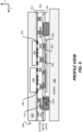
- FIG. 1 illustrates a package 100 that includes a substrate 102, an integrated device 104, and an encapsulation layer 108.
- the substrate 102 includes at least one dielectric layer 120, a plurality of interconnects 122, and a plurality of solder interconnects 124.
- a plurality of solder interconnects 144 is coupled to the substrate 102 and the integrated device 104.
- the encapsulation layer 108 encapsulates the integrated device 104 and the plurality of solder interconnects 144. Fabricating a small package that includes a substrate with high density interconnects can be challenging. There is an ongoing need to provide more compact packages that can accommodate high density interconnects and/or high pin counts.
- US 2015/0116965 A1 discloses a semiconductor package comprising an interposer and a package substrate.
- the invention according to independent claim 1 provides a package comprising a substrate and an integrated device coupled to the substrate.
- the substrate includes (i) at least one inner dielectric layer, (ii) a plurality of interconnects located in the at least one inner dielectric layer, where the plurality of interconnects includes a pad located on a bottom metal layer of the substrate, (iii) an outer dielectric layer located over the at least one inner dielectric layer, (iv) at least one routing interconnect coupled to the plurality of interconnects, where the at least one routing interconnect is located over the outer dielectric layer, where the at least one routing interconnect is located over the bottom metal layer of the substrate, and (v) a cover dielectric layer located over the outer dielectric layer and the at least one routing interconnect.
- the package includes a solder interconnect coupled to the pad located on the bottom metal layer of the substrate.
- the invention according to independent claim 14 provides a method for fabricating a package.
- the method provides a substrate.
- the substrate includes (i) at least one inner dielectric layer; (ii) a plurality of interconnects located in the at least one inner dielectric layer, wherein the plurality of interconnects includes a pad located on a bottom metal layer of the substrate; (iii) an outer dielectric layer located over the at least one inner dielectric layer; (iv) at least one routing interconnect coupled to the plurality of interconnects, wherein the at least one routing interconnect is located over the outer dielectric layer, wherein the at least one routing interconnect is located over the bottom metal layer of the substrate, and (v) a cover dielectric layer located over the outer dielectric layer and the at least one routing interconnect.
- the method couples an integrated device to the substrate.
- the method couples a solder interconnect to the pad located on the bottom metal layer of the substrate.
- the present disclosure describes a package that includes a substrate and an integrated device coupled to the substrate.
- the substrate includes (i) at least one inner dielectric layer, (ii) a plurality of interconnects located at least in the at least one inner dielectric layer, where the plurality of interconnects includes a pad located on a bottom metal layer of the substrate, (iii) an outer dielectric layer located over the at least one inner dielectric layer, (iv) at least one routing interconnect coupled to the plurality of interconnects, where the at least one routing interconnect is located over the outer dielectric layer, where the at least one routing interconnect is located over the bottom metal layer of the substrate, and (v) a cover dielectric layer located over the outer dielectric layer and the at least one routing interconnect, the cover dielectric layer may be coupled to the outer dielectric layer.
- the package includes a solder interconnect coupled to the pad located on the bottom metal layer of the substrate.
- the outer dielectric layer may include a solder resist layer or photo imageable dielectric (PID).
- the cover dielectric layer may include a solder resist layer or photo imageable dielectric (PID).
- the at least one routing interconnect may be located (e.g., laterally located) between a plurality of solder interconnects.
- the integrated device and the substrate are coupled together in such a way that a first electrical signal to and/or from the integrated device, may be configured to travel through the plurality of interconnects and the at least routing interconnect located over the outer dielectric layer substrate.
- This configuration where the at least one routing interconnect is located over an outer dielectric layer and between solder interconnects, may allow the space (e.g., lateral space) between solder interconnects of the substrate to be utilized for routing, providing more routing real estate without increasing the overall size and form of the substrate and/or the package.
- Exemplary Package Comprising a Substrate With Interconnects Located Over an Outer Dielectric Layer
- FIG. 2 illustrates a profile view of a package 200 that includes interconnects located over an outer dielectric layer.
- the package 200 is coupled to a board 290 (e.g., printed circuit board (PCB)) through a plurality of solder interconnects 280.
- PCB printed circuit board
- the package 200 provides a package with a compact small factor while also having an improved routing interconnect design.
- the package 200 includes a substrate 202, a first integrated device 205, a second integrated device 206, an encapsulation layer 208 and the plurality of solder interconnects 280.
- the substrate 202 includes a first surface (e.g., top surface) and a second surface (e.g., bottom surface).
- the substrate 202 includes at least one inner dielectric layer 220, a plurality of interconnects 222, a solder resist layer 224, an outer dielectric layer 230, a cover dielectric layer 240, and at least one routing interconnect 242.
- the plurality of interconnects 222 is located at least in and over the at least one inner dielectric layer 220.
- the plurality of interconnects 222 includes at least one pad 222a located on a bottom metal layer of the substrate 202.
- the pad 222a is configured to be coupled to a solder interconnect from the plurality of solder interconnects 280.
- the outer dielectric layer 230 is located over the at least one dielectric layer 220.
- the at least one routing interconnect 242 is coupled to the plurality of interconnects 222.
- the at least one routing interconnect 242 is located over the outer dielectric layer 230.
- the at least one routing interconnect 242 is located over (or under, depending on how top and bottom are arbitrarily defined) the bottom metal layer of substrate 202.
- the at least one routing interconnect 242 may be located between the bottom metal layer of substrate 202 and the board 290.
- the cover dielectric layer 240 is located over the outer dielectric layer 230 and the at least one routing interconnect 242.
- the at least one routing interconnect 242 may be means for routing interconnect.
- the cover dielectric layer 240 may be coupled to the outer dielectric layer 230.
- the particular dielectric layer when a particular dielectric layer is located “over" another dielectric layer, the particular dielectric layer may be located above or below the another dielectric layer, depending on how a bottom (e.g., bottom layer) or top (e.g., top layer) is arbitrarily defined.
- a particular dielectric layer that is located "over" another dielectric layer may mean that the particular dielectric layer is coupled to a surface of the another dielectric layer. For example, a surface of the particular dielectric layer may be in contact (e.g., touching) with another surface of the another dielectric layer.
- the outer dielectric layer 230 may be coupled and located over (e.g., below) a bottom surface of the at least one inner dielectric layer 220.
- the at least one routing interconnect 242 and the cover dielectric layer 240 may be coupled and located over (e.g., below) a bottom surface of the outer dielectric layer 230.
- the at least one routing interconnect 242 may be located laterally between the plurality of solder interconnects 280.
- the at least one routing interconnect 242 may be free of direct contact with the plurality of solder interconnects 280.
- the at least one routing interconnect 242 may be coupled to the plurality of interconnects 222.
- the outer dielectric layer 230, the cover dielectric layer 240 and the at least one routing interconnect 242 may be part of the substrate 202.
- the bottom metal layer of the substrate 202 may be a metal layer of the substrate 202 that includes interconnects (such as pads) that are configured to be coupled to solder interconnects.
- the bottom metal layer of the substrate 202 may not be necessarily the lowest metal layer of the substrate 202 or the metal layer of the substrate 202 that is closest to a board (when the substrate 202 is coupled to a board).
- the bottom metal layer of the substrate 202 may be the metal layer that includes the interconnects (such as pad 222a) that are coupled (e.g., directly coupled) to the plurality of solder interconnects 280.
- the plurality of solder interconnects 280 is further coupled to the board 290 (e.g., printed circuit board).
- the bottom metal layer of the substrate 202 may be a metal layer that is closest (e.g., vertically closest) to the plurality of solder interconnects 280 without being laterally positioned (e.g., along X-axis and/or Y-axis) along a same plane as the plurality of solder interconnects 280.
- a bottom metal layer of a substrate may be defined as to not include metal layer(s) that are located laterally to the plurality of solder interconnects 280.
- the plurality of solder interconnects 280 is coupled to the substrate 202 (e.g., coupled to the bottom metal layer of the substrate 202) such that the at least one routing interconnect 242 is located laterally to the plurality of solder interconnects 280 and/or located between the plurality of solder interconnects 280.
- the use of the at least one routing interconnect 242 helps save space and helps reduce the overall height and footprint of the package 200, utilizing space that would not otherwise be used. Moreover, the use of the at least one routing interconnect 242 may help reduce routing congestion (e.g., local routing congestion) in the substrate 202.
- the at least one routing interconnect 242 may also be formed over another surface (e.g., top surface) of the substrate 202.
- another cover dielectric layer and/or outer dielectric may be formed over the second surface of the substrate 202.
- at least one routing interconnect, a cover dielectric layer and/or an outer dielectric layer may be formed over a bottom surface and/or a top surface of the substrate 202.
- the outer dielectric layer 230 may include a different material than the at least one inner dielectric layer 220.
- the cover dielectric layer 240 may include a different material than the at least one inner dielectric layer 220.
- the cover dielectric layer 240 may include a different material than the at least one inner dielectric layer 220 and the outer dielectric layer 230.
- the cover dielectric layer 240 and the outer dielectric layer 230 may each include a different material than the at least one inner dielectric layer 220.
- the cover dielectric layer 240 and the outer dielectric layer 230 may include the same material.
- the at least one inner dielectric layer 220 may include a copper clad laminate (CCL) core, a prepreg, an ajinomoto build up film (ABF), and/or a resin coated copper (RCC).
- the outer dielectric layer 230 may include a solder resist layer and/or a photo imageable dielectric (PID).
- the cover dielectric layer 240 may include a solder resist layer and/or a photo imageable dielectric (PID).
- the first integrated device 205 is coupled to a first surface (e.g., top surface) of the substrate 202 through a plurality of interconnects 250.
- the plurality of interconnects 250 may include copper pillars and/or solder interconnects.
- the second integrated device 206 is coupled to the first surface of the substrate 202 through a plurality of interconnects 260.
- the plurality of interconnects 260 may include copper pillars and/or solder interconnects.
- the encapsulation layer 208 is located over and coupled to the first surface of the substrate 202 and may encapsulate the first integrated device 205 and the second integrated device 206.
- the encapsulation layer 208 may include a mold, a resin, an epoxy and/or polymer.
- the encapsulation layer 208 may be means for encapsulation.
- the integrated device may include a die (e.g., semiconductor bare die).
- the integrated device may include a radio frequency (RF) device, a passive device, a filter, a capacitor, an inductor, an antenna, a transmitter, a receiver, a GaAs based integrated device, a surface acoustic wave (SAW) filters, a bulk acoustic wave (BAW) filter, a light emitting diode (LED) integrated device, a silicon carbide (SiC) based integrated device, memory, and/or combinations thereof.
- RF radio frequency
- a passive device e.g., a filter, a capacitor, an inductor, an antenna, a transmitter, a receiver, a GaAs based integrated device, a surface acoustic wave (SAW) filters, a bulk acoustic wave (BAW) filter, a light emitting diode (LED) integrated device, a silicon carbide (SiC) based integrated device, memory,
- Different implementations may couple different components to the substrate 202.
- Other components e.g., surface mounted components
- a passive device e.g., capacitor
- Some electrical signals may travel through the plurality of interconnects 222 and the at least one routing interconnect 242.
- some signals to and/or from an integrated device may travel through a first plurality of interconnects from the plurality of interconnects 222, the at least one routing interconnect 242 and a second plurality of interconnects from the plurality of interconnects 222.
- the at least one routing interconnect 242 may allow the package 200 to provide higher I/O pin counts, without having to increase the size of the package 200.
- using the at least one routing interconnect 242 may allow the substrate 202 to have a lower number of metal layers, which may help reduce the overall height of the package 200.
- the at least one routing interconnect 242 may help reduce congestion and/or entanglement in certain regions (e.g., regions near an integrated device) of the substrate 202 due to the high number of pin count and/or number of netlists.
- a netlist is an arrangement of components of a circuit and how the components are electrically coupled together.
- the substate 202 may include a core layer.
- the substrate 202 may be a coreless substrate.
- the substrate 202 may be fabricated using different fabrication processes, including a semi-additive process (SAP) and a modified semi-additive process (mSAP).
- SAP semi-additive process
- mSAP modified semi-additive process
- the plurality of interconnects 222 and the at least one routing interconnect 242 may have different shapes and/or sizes.
- the plurality of interconnects 222 may include a redistribution interconnect.
- the at least one routing interconnect 242 may include at least one routing redistribution interconnect.
- a redistribution interconnect may be fabricated using redistribution layer (RDL) fabrication process. Examples of a method for fabricating a substate are illustrated and described below in FIGS. 5A-5F and 6A-6B .
- FIG. 3 illustrates an exemplary bottom plan view of the package 200.
- the plurality of solder interconnects 280 is coupled to the substrate 202.
- the substrate 202 includes the outer dielectric layer 230, the at least one routing interconnect 242 and the cover dielectric layer 240.
- the at least one routing interconnect 242 is located over the outer dielectric layer 230.
- the cover dielectric layer 240 is located over the at least one routing interconnect 242 and the outer dielectric layer 230.
- the at least one routing interconnect 242 is located (e.g., laterally located) between the plurality of solder interconnects 280.
- the at least one routing interconnect 242 which may include at least one routing pad, at least one routing trace and/or at least one routing via, may travel in and/or along a surface of the outer dielectric layer 230.
- the at least one routing interconnect 242 may be located (e.g., located laterally) between the plurality of solder interconnects 280.
- FIG. 4 illustrates a package 400 that includes the substrate 402.
- the package 400 is similar to the package 200, and thus includes similar components as the package 200.
- the substrate 402 is similar to the substrate 202, and thus includes similar components as the substrate 202.
- the substrate 402 includes a first surface (e.g., top surface) and a second surface (e.g., bottom surface).
- the substrate 402 includes at least one inner dielectric layer 220, a plurality of interconnects 222, a solder resist layer 224, an outer dielectric layer 230, an outer dielectric layer 430, a cover dielectric layer 240, and at least one routing interconnect 242.
- the plurality of interconnects 222 is located at least in and over the at least one inner dielectric layer 220.
- the plurality of interconnects 222 includes at least one pad 222a located on a bottom metal layer of the substrate 402.
- the pad 222a is configured to be coupled to a solder interconnect from the plurality of solder interconnects 280.
- the at least one routing interconnect 242 is coupled to the plurality of interconnects 222.
- the at least one routing interconnect 242 is located over the cover dielectric layer 240.
- the at least one routing interconnect 242 is located over (or under, depending on how top and bottom are arbitrarily defined) the bottom metal layer of substrate 402.
- the outer dielectric layer 230 may be located over the at least one inner dielectric layer 220.
- the outer dielectric layer 230 may be located laterally to the cover dielectric layer 240.
- the outer dielectric layer 430 is located over the cover dielectric layer 240 and the at least one routing interconnect 242.
- the outer dielectric layer 430 may be a second outer dielectric layer.
- the outer dielectric layer 430 may be considered part of the outer dielectric layer 230, and vice versa.
- an outer dielectric layer (which may include the outer dielectric layer 230 and the outer dielectric layer 430) may be located over (e.g., below) the at least one inner dielectric layer 220, the cover dielectric layer 240, and the at least one routing interconnect 242.
- the cover dielectric laser 240 may located between the at least one inner dielectric layer 220 and the outer dielectric layer 430.
- the cover dielectric laser 240 may be coupled to the at least one inner dielectric layer 220 and the outer dielectric layer 430.
- the particular dielectric layer when a particular dielectric layer is located “over" another dielectric layer, the particular dielectric layer may be located above or below the another dielectric layer, depending on how a bottom (e.g., bottom layer) or top (e.g., top layer) is arbitrarily defined.
- a particular dielectric layer that is located "over" another dielectric layer may mean that the particular dielectric layer is coupled to a surface of the another dielectric layer. For example, a surface of the particular dielectric layer may be in contact (e.g., touching) with another surface of the another dielectric layer.
- the outer dielectric layer 230 may be coupled and located over (e.g., below) a bottom surface of the at least one inner dielectric layer 220.
- the cover dielectric layer 240 may be coupled and located over (e.g., below) a bottom surface of the at least one inner dielectric layer 220.
- the cover dielectric layer 240 may be co-planar to the outer dielectric layer 230.
- the at least one routing interconnect 242 may be coupled and located over (e.g., below) a bottom surface of the cover dielectric layer 240.
- the outer dielectric layer 430 may be located over (e.g., below) the at least one routing interconnect 242 and a bottom surface of the cover dielectric layer 240.
- the at least one routing interconnect 242 may be located laterally between the plurality of solder interconnects 280.
- the at least one routing interconnect 242 may be free of direct contact with the plurality of solder interconnects 280.
- the at least one routing interconnect 242 may be coupled to the plurality of interconnects 222.
- the outer dielectric layer 230, the outer dielectric layer 430, the cover dielectric layer 240 and the at least one routing interconnect 242 may be part of the substrate 402.
- the at least one routing interconnect 242 may also be formed over the first surface (e.g., top surface) of the substrate 402. In such an instance, another cover dielectric layer and/or outer dielectric may be formed over the first surface of the substrate 402. Thus, in some implementations, at least one routing interconnect, a cover dielectric layer and/or an outer dielectric layer may be formed over a bottom surface and/or a top surface of the substrate 402.
- the outer dielectric layer (e.g., 230, 430) may include a different material than the at least one inner dielectric layer 220.
- the cover dielectric layer 240 may include a different material than the at least one inner dielectric layer 220.
- the cover dielectric layer 240 may include a different material than the at least one inner dielectric layer 220 and the outer dielectric layer (e.g., 230, 430).
- the cover dielectric layer 240 and the outer dielectric layer (e.g., 230, 430), may each include a different material than the at least one inner dielectric layer 220.
- the cover dielectric layer 240 and the outer dielectric layer (e.g., 230, 430) may include the same material.
- fabricating a substrate includes several processes.
- FIG. 5 (which includes FIGS. 5A-5F ) illustrates an exemplary sequence for providing or fabricating a substrate.
- the sequence of FIGS. 5A-5F may be used to provide or fabricate the substrate 202 of FIG. 2 .
- the process of FIGS. 5A-5F may be used to fabricate any of the substrates described in the disclosure.
- FIGS. 5A-5F may combine one or more stages in order to simplify and/or clarify the sequence for providing or fabricating a substrate.
- the order of the processes may be changed or modified.
- one or more of processes may be replaced or substituted.
- Stage 1 illustrates a state after a carrier 500 is provided and a metal layer is formed over the carrier 500.
- the metal layer may be patterned to form interconnects 502.
- a plating process and etching process may be used to form the metal layer and interconnects.
- Stage 2 illustrates a state after a dielectric layer 520 is formed over the carrier 500 and the interconnects 502.
- the dielectric layer 520 may include polyimide. However, different implementations may use different materials for the dielectric layer.
- the dielectric layer 520 may be an inner dielectric layer.
- Stage 3 illustrates a state after at least one cavity 510 is formed in the dielectric layer 520.
- the at least one cavity 510 may be formed using an etching process (e.g., photo etching process) or laser process.
- Stage 4 illustrates a state after interconnects 512 are formed in and over the dielectric layer 520.
- interconnects 512 For example, a via, pad and/or traces may be formed.
- a plating process may be used to form the interconnects.
- the interconnects 512 may be part of the plurality of interconnects 222.
- Stage 5 illustrates a state after another dielectric layer 522 is formed over the dielectric layer 520.
- the dielectric layer 522 may be the same material as the dielectric layer 520. However, different implementations may use different materials for the dielectric layer.
- the dielectric layer 522 may be an inner dielectric layer.
- Stage 6 illustrates a state after at least one cavity 530 is formed in the dielectric layer 522.
- An etching process or laser process may be used to form the at least one cavity 530.
- Stage 7 illustrates a state after interconnects 514 are formed in and over the dielectric layer 522.
- interconnects 514 For example, via, pad and/or trace may be formed.
- a plating process may be used to form the interconnects.
- the interconnects 514 may be part of the plurality of interconnects 222.
- Stage 8 illustrates a state after another dielectric layer 524 is formed over the dielectric layer 522.
- the dielectric layer 524 may be the same material as the dielectric layer 520. However, different implementations may use different materials for the dielectric layer.
- the dielectric layer 524 may be an inner dielectric layer.
- Stage 9 illustrates a state after at least one cavity 540 is formed in the dielectric layer 524.
- An etching process or laser process may be used to form the at least one cavity 540.
- Stage 10 illustrates a state after interconnects 516 are formed in and over the dielectric layer 524.
- interconnects 516 For example, via, pad and/or trace may be formed.
- a plating process may be used to form the interconnects.
- interconnects 502, 512, 514 and/or 516 may define the plurality of interconnects 222 of the substrate 202.
- the dielectric layers 520, 522, 524 may be represented by the at least one inner dielectric layer 220.
- Stage 11 illustrates a state after the carrier 500 is decoupled (e.g., removed, grinded out) from the at least one inner dielectric layer 220, leaving the substrate 202.
- Stage 12 illustrates a state after the solder resist layer 224 and the outer dielectric layer 230 are formed over the substrate 202.
- a deposition process may be used to dispose the solder resist layer 224 and the outer dielectric layer 230 over the substrate 202.
- the solder resist layer 224 may be disposed over (e.g., above) a first surface (e.g., top surface) of the at least one inner dielectric layer 220
- the outer dielectric layer 230 may be disposed over (e.g., below) a second surface (e.g., bottom surface) of the at least one inner dielectric layer 220.
- a top surface and a bottom surface may be defined arbitrarily. Different implementations may define a top or a bottom differently.
- Stage 13 illustrates a state after cavities 560 are formed in the outer dielectric layer 230.
- a laser process and/or an etching process may be used to form the cavities 560.
- Stage 14 illustrates a state after a mask 570 is formed over the outer dielectric layer 230.
- Stage 15 illustrates a state after portions of the mask 570 are opened, exposing portions of the outer dielectric layer 230 and some of the interconnects from the plurality of interconnects 222.
- An etching process may be used to open portions of the mask 570.
- Stage 16 illustrates a state after at least one routing interconnect 242 is formed in and over the outer dielectric layer 230.
- a routing via, a routing pad and/or a routing trace may be formed.
- a plating process may be used to form the routing interconnects.
- Stage 17 illustrates a state after the cover dielectric layer 240 is formed over the at least one routing interconnect 242 and the outer dielectric layer 230.
- a deposition process may be used to dispose the cover dielectric layer 240 over the at least one routing interconnect 242 and the outer dielectric layer 230.
- Stage 18 illustrates a state after the mask 570 is removed.
- An etching process may be used to remove or couple the mask 570.
- Stage 19 illustrates a state after a solder interconnect (from the plurality of solder interconnects 280) is coupled to the plurality of interconnects 222.
- the solder interconnect 280 may be coupled to the pad 222a (which is part of the plurality of interconnects 222).
- the pad 222a may be located on a bottom metal layer of the substrate 202.
- Stage 19 may illustrate the substrate 202 that includes at least one routing interconnect 242 located between solder interconnects 280, as described in FIG. 2 .
- a chemical vapor deposition (CVD) process and/or a physical vapor deposition (PVD) process for forming the metal layer(s).
- CVD chemical vapor deposition
- PVD physical vapor deposition
- a sputtering process, a spray coating process, and/or a plating process may be used to form the metal layer(s).
- fabricating a substrate includes several processes.
- FIG. 6 (which includes FIGS. 6A-6B ) illustrates an exemplary sequence for providing or fabricating a substrate.
- the sequence of FIGS. 6A-6B may be used to provide or fabricate the substrate 402 of FIG. 4 .
- the process of FIGS. 6A-6B may be used to fabricate any of the substrates described in the disclosure.
- FIGS. 6A-6B may combine one or more stages in order to simplify and/or clarify the sequence for providing or fabricating a substrate.
- the order of the processes may be changed or modified.
- one or more of processes may be replaced or substituted.
- Stage 1 illustrates a state after a substrate 402 that includes the at least one inner dielectric layer 220 and the plurality of interconnects 222, is provided.
- the substrate 402 of Stage 1 of FIG. 6A may be similar to the substrate 202 of Stage 11 of FIG. 5C .
- the substrate 402 of Stage 1 of FIG. 6A may be fabricated as shown and described in Stages 1-11 of FIGS. 5A-5C .
- Stage 2 illustrates a state after the solder resist layer 224 and the cover dielectric layer 240 are formed over the substrate 402.
- a deposition process may be used to dispose the solder resist layer 224 and the cover dielectric layer 240 over the substrate 402.
- Stage 3 illustrates a state after portions of the cover dielectric layer 240 are removed and cavities 640 are formed in the cover dielectric layer 240.
- a laser process and/or an etching process may be used to form the cavities 640 and/or remove portions of the cover dielectric layer 240.
- Stage 4 illustrates a state after at least one routing interconnect 242 is formed in and over the cover dielectric layer 240.
- a routing via, a routing pad and/or a routing trace may be formed.
- a plating process may be used to form the routing interconnects.
- Stage 5 illustrates a state after the outer dielectric layer 230 is formed over the at least one routing interconnect 242 and the cover dielectric layer 240.
- a deposition process may be used to dispose the outer dielectric layer 230 over the at least one routing interconnect 242 and the cover dielectric layer 240.
- a laser process and/or an etching process may be used to form the cavity 630 in the outer dielectric layer 230.
- Stage 6 illustrates a state after a solder interconnect (from the plurality of solder interconnects 280) is coupled to the plurality of interconnects 222.
- the solder interconnect 280 may be coupled to the pad 222a (which is part of the plurality of interconnects 222).
- the pad 222a may be located on a bottom metal layer of the substrate 402.
- Stage 6 may illustrate the substrate 402 that includes at least one routing interconnect 242 located between solder interconnects 280, as described in FIG. 4 .
- a chemical vapor deposition (CVD) process and/or a physical vapor deposition (PVD) process for forming the metal layer(s).
- CVD chemical vapor deposition
- PVD physical vapor deposition
- a sputtering process, a spray coating process, and/or a plating process may be used to form the metal layer(s).
- fabricating a substrate includes several processes.
- FIG. 7 illustrates an exemplary flow diagram of a method 700 for providing or fabricating a substrate.
- the method 700 of FIG. 7 may be used to provide or fabricate the substrate of FIG. 2 .
- the method of FIG. 7 may be used to fabricate the substrate 202 and/or the substrate 402.
- the method of FIG. 7 may combine one or more processes in order to simplify and/or clarify the method for providing or fabricating a substrate.
- the order of the processes may be changed or modified.
- the method provides (at 705) a carrier 500.
- a carrier 500 may include a substrate, glass, quartz and/or carrier tape.
- Stage 1 of FIG. 5A illustrates a state after a carrier is provided.
- the method forms (at 710) a metal layer over the carrier 500.
- the metal layer may be patterned to form interconnects.
- a plating process may be used to form the metal layer and interconnects.
- Stage 1 of FIG. 5A illustrates a state after a metal layer and interconnects 502 are formed.
- the method forms (at 715) at least one inner dielectric layer (e.g., dielectric layer 520) over the carrier 500 and the interconnects 502.
- the dielectric layer 520 may include polyimide.
- Forming the dielectric layer may also include forming a plurality of cavities (e.g., 510) in the dielectric layer 520.
- a deposition process may be used to form the at least one inner dielectric layer.
- the plurality of cavities may be formed using an etching process (e.g., photo etching) or laser process.
- Stages 2-3 of FIG. 5A illustrate forming a dielectric layer and cavities in the dielectric layer.
- the method forms (at 720) interconnects in and over the inner dielectric layer.
- the interconnects 512 may be formed in and over the dielectric layer 520.
- a plating process may be used to form the interconnects.
- Forming interconnects may include providing a patterned metal layer over and/or in the dielectric layer.
- Stage 4 of FIG. 5A illustrates an example of forming interconnects in and over a dielectric layer.
- stages 2-10 of FIGS. 5A-5C illustrate examples of forming at least one inner dielectric layer and a plurality of interconnects in and over the inner dielectric layer(s).
- the method forms (at 725) an outer dielectric layer 230 over the at least one inner dielectric layer 220 and the plurality of interconnects 222.
- the outer dielectric layer 230 may include a solder resist layer or a photo imageable dielectric (PID).
- a deposition process may be used to form the outer dielectric layer 230.
- Forming the outer dielectric layer may also include forming a plurality of cavities (e.g., 530) in the outer dielectric layer 230.
- the plurality of cavities may be formed using an etching process or laser process. Stages 12-13 of FIGS. 5C-15D illustrate forming an outer dielectric layer and cavities in the outer dielectric layer.
- the method forms (at 730) routing interconnects in and/or over the outer dielectric layer.
- the at least one routing interconnect 242 may be formed.
- a plating process may be used to form the routing interconnects.
- Forming routing interconnects may include providing a patterned metal layer over an in the outer dielectric layer 230.
- Stages 14-16 of FIGS. 5D-5E may illustrate an example of forming interconnects in and over an outer dielectric layer.
- the method forms (at 735) a cover dielectric layer (e.g., 240) over the outer dielectric layer 230 and the at least one routing interconnect 242.
- the cover dielectric layer 240 may include a solder resist layer or a photo imageable dielectric (PID).
- a deposition process may be used to form the cover dielectric layer 240.
- Stages 17-19 of FIGS. 5E-5F may illustrate an example of forming a cover dielectric layer.
- the method may form the dielectric layers in different order.
- at least one cover dielectric layer may be formed before at least one outer dielectric layer is formed.
- Such an example is described in at least FIGS. 6A-6B above.
- Different implementations may use different processes for forming the metal layer(s).
- CVD chemical vapor deposition
- PVD physical vapor deposition
- a sputtering process, a spray coating process, and/or a plating process may be used to form the metal layer(s).
- FIG. 8 (which includes FIGS. 8A-8B ) illustrates an exemplary sequence for providing or fabricating a package that includes a substrate.
- the sequence of FIGS. 8A-8B may be used to provide or fabricate the package 200 that includes the substrate 202 of FIG. 2 , or any of the packages described in the disclosure.
- FIGS. 8A-8B may combine one or more stages in order to simplify and/or clarify the sequence for providing or fabricating the package.
- the order of the processes may be changed or modified.
- one or more of processes may be replaced or substituted.
- the sequence of FIGS. 8A-8B may be used to fabricate one package or several packages at a time (as part of a wafer).
- Stage 1 illustrates a state after the substrate 202 is provided.
- the substrate 202 may be provided by a supplier or fabricated.
- a process similar to the process shown in FIGS. 5A-5F may be used to fabricate the substrate 202.
- different implementations may use different processes to fabricate the substrate 202. Examples of processes that may be used to fabricate the substrate 202 include a semi-additive process (SAP) and a modified semi-additive process (mSAP).
- SAP semi-additive process
- mSAP modified semi-additive process
- the substrate 202 includes a first surface (e.g., top surface) and a second surface (e.g., bottom surface).
- the substrate 202 includes at least one inner dielectric layer 220, a plurality of interconnects 222, a solder resist layer 224, an outer dielectric layer 230, a cover dielectric layer 240, and at least one routing interconnect 242.
- the plurality of interconnects 222 is located at least in and over the at least one inner dielectric layer 220.
- the plurality of interconnects 222 includes at least one pad 222a located on a bottom metal layer of the substrate 202.
- the pad 222a is configured to be coupled to a solder interconnect from the plurality of solder interconnects 280.
- the outer dielectric layer 230 is located over the at least one inner dielectric layer 220.
- the at least one routing interconnect 242 is coupled to the plurality of interconnects 222.
- the at least one routing interconnect 242 is located over the outer dielectric layer 230.
- the at least one routing interconnect 242 is located over (or under, depending on how top and bottom are arbitrarily defined) the bottom metal layer of substrate 202.
- the cover dielectric layer 240 is located over the outer dielectric layer 230 and the at least one routing interconnect 242.
- Stage 2 illustrates a state after the plurality of solder interconnects 280 is coupled to the substrate 202.
- the solder interconnect 280 may be coupled to a bottom metal layer of the substrate 202.
- the solder interconnect 280 may be coupled to the pad 222a (which is located on a bottom metal layer) of the substrate 202.
- a reflow process may be used to couple the solder interconnect 280 to the substrate 202.
- Stage 3 illustrates a state after the first integrated device 205 is coupled to a first surface (e.g., top surface) of the substrate 202 through the plurality of interconnects 250.
- the plurality of interconnects 250 may be coupled to interconnects from the plurality of interconnects 222 of the substrate 202.
- Stage 3 also illustrates a state after the second integrated device 206 is coupled to the first surface (e.g., top surface) of the substrate 202 through the plurality of interconnects 260.
- the plurality of interconnects 260 may be coupled to interconnects from the plurality of interconnects 222 of the substrate 202.
- a reflow process may be used to couple the first integrated device 205 and/or the second integrated device 206 to the substrate 202.
- Stage 4 illustrate a state after the encapsulation layer 208 is formed over the first surface of the substrate 202 such that the encapsulation layer 208 encapsulates the first integrated device 205 and the second integrated device 206.
- the process of forming and/or disposing the encapsulation layer 208 may include using a compression and transfer molding process, a sheet molding process, or a liquid molding process.
- Stage 4 may illustrate the package 200 that includes the substrate 202, the first integrated device 205, the second integrated device 206 and the encapsulation layer 208.
- the packages (e.g., 200, 400) described in the disclosure may be fabricated one at a time or may be fabricated together as part of one or more wafers and then singulated into individual packages.
- fabricating a package that includes a substrate includes several processes.
- FIG. 9 illustrates an exemplary flow diagram of a method 900 for providing or fabricating a package that includes a substrate.
- the method 900 of FIG. 9 may be used to provide or fabricate the package 200 of FIG. 2 described in the disclosure.
- the method 900 may be used to provide or fabricate any of the packages described in the disclosure.
- the method of FIG. 9 may combine one or more processes in order to simplify and/or clarify the method for providing or fabricating a package that a substrate.
- the order of the processes may be changed or modified.
- the method provides (at 905) a substrate (e.g., 202, 402).
- the substrate 202 may be provided by a supplier or fabricated.
- the substrate 202 includes a first surface (e.g., top surface) and a second surface (e.g., bottom surface).
- the substrate 202 may include at least one inner dielectric layer 220, a plurality of interconnects 222, a solder resist layer 224, an outer dielectric layer 230, a cover dielectric layer 240, and at least one routing interconnect 242.
- the plurality of interconnects 222 is located at least in and over the at least one inner dielectric layer 220.
- the plurality of interconnects 222 includes at least one pad 222a located on a bottom metal layer of the substrate 202.
- the pad 222a is configured to be coupled to a solder interconnect from the plurality of solder interconnects 280.
- the outer dielectric layer 230 is located over the at least one inner dielectric layer 220.
- the at least one routing interconnect 242 is coupled to the plurality of interconnects 222.
- the at least one routing interconnect 242 is located over the outer dielectric layer 230.
- the at least one routing interconnect 242 is located below the bottom metal layer of substrate 202.
- the cover dielectric layer 240 is located over the outer dielectric layer 230 and the at least one routing interconnect 242.
- Stage 1 of FIG. 8A illustrates and describes an example of providing a substrate.
- the method couples (at 910) the plurality of solder interconnects (e.g., 280) to the substrate (e.g., 202).
- the solder interconnect 280 may be coupled to a bottom metal layer of the substrate 202.
- the solder interconnect 280 may be coupled to the pad 222a (which is located on a bottom metal layer) of the substrate 202.
- a reflow process may be used to couple the solder interconnect 280 to the substrate 202.
- Stage 2 of FIG. 8A illustrates and describes an example of coupling solder interconnects to a substrate.
- the method couples (at 915) components to the substrate (e.g., 202).
- the method may couple the first integrated device 205 to a first surface (e.g., top surface) of the substrate 202 through the plurality of interconnects 250.
- the plurality of interconnects 250 may be coupled to interconnects from the plurality of interconnects 222 of the substrate 202.
- the method may couple the second integrated device 206 to a first surface (e.g., top surface) of the substrate 202 through the plurality of interconnects 260.
- the plurality of interconnects 260 may be coupled to interconnects from the plurality of interconnects 222 of the substrate 202.
- a reflow process may be used to couple the first integrated device 205 and/or the second integrated device 206 to the substrate 202.
- Stage 3 of FIG. 8B illustrates and describes an example of coupling components to a substrate.
- the method forms (at 925) an encapsulation layer (e.g., 208) over the first surface of the substrate (e.g., 202).
- the encapsulation layer may be formed over the first surface of the substrate such that the encapsulation layer 208 encapsulates the first integrated device 205 and the second integrated device 206 (which are example of components).
- the process of forming and/or disposing the encapsulation layer 208 may include using a compression and transfer molding process, a sheet molding process, or a liquid molding process.
- Stage 4 of FIG. 8B illustrates and describes an example of an encapsulation layer that is located over the substrate and encapsulates the integrated device.
- PoP Package on Package
- FIG. 10 illustrates a profile view of a package on package (PoP) 1000 that includes a package 1001 and a package 1003 that includes interconnects located over an outer dielectric layer.
- the package 1001 is coupled to the package 1003 through the plurality of solder interconnects 1080.
- the package 1001 is located over the package 1003.
- the PoP 1000 is coupled to a board 290 (e.g., printed circuit board (PCB)) through a plurality of solder interconnects 280 of the package 1003.
- the package 1003 provides a package with a compact small factor while also having an improved routing interconnect design.
- PCB printed circuit board
- the package 1003 of FIG. 10 is similar to the package 200 of FIG. 2 , and thus include similar components as the package 200.
- the package 1003 includes a plurality of vias 1088 that travel through the encapsulation layer 208.
- the plurality of vias 1088 may include through mold vias (TMVs).
- TMVs through mold vias
- the plurality of vias 1088 is coupled to the plurality of interconnects 222.
- the package 1003 includes a plurality of upper routing interconnects 1042 that is located over the encapsulation layer 208.
- the plurality of upper routing interconnects 1042 may be coupled to the plurality of vias 1088.
- An upper cover dielectric layer 1040 is located over the plurality of upper routing interconnects 1042 and the encapsulation layer 208.
- the plurality of upper routing interconnects 1042 is located (e.g., laterally located) between the plurality of solder interconnects 1080.
- the plurality of upper routing interconnects 1042 may be means for upper routing interconnect.
- An encapsulation layer 1070 may be located between the package 1001 and the package 1003.
- the package 1001 includes a substrate 1002, an integrated device 1006, and an encapsulation layer 1008.
- the substrate 1002 includes at least one dielectric layer 1020 and a plurality of interconnects 1022.
- the integrated device 1006 is coupled to the substrate 1002.
- the encapsulation layer 1008 is coupled to the substrate 1002 and encapsulates the integrated device 1006.
- the package 1001 may be similar to the package 200, and thus the package 1001 may include an outer dielectric layer (e.g., 230) and/or a cover dielectric layer (e.g., 240).
- an outer dielectric layer e.g., 230
- a cover dielectric layer e.g., 240
- the particular dielectric layer when a particular dielectric layer is located “over" another dielectric layer, the particular dielectric layer may be located above or below the another dielectric layer, depending on how a bottom (e.g., bottom layer) or top (e.g., top layer) is arbitrarily defined.
- a particular dielectric layer that is located "over" another dielectric layer may mean that the particular dielectric layer is coupled to a surface of the another dielectric layer. For example, a surface of the particular dielectric layer may be in contact (e.g., touching) another surface of the another dielectric layer.
- PoP Package on Package
- FIG. 11 (which includes FIGS. 11A-11C ) illustrates an exemplary sequence for providing or fabricating a package on package (PoP).
- the sequence of FIGS. 11A-11C may be used to provide or fabricate the PoP 1000 of FIG. 10 , or any of the PoPs described in the disclosure.
- FIGS. 11A-11C may combine one or more stages in order to simplify and/or clarify the sequence for providing or fabricating the PoP.
- the order of the processes may be changed or modified.
- one or more of processes may be replaced or substituted.
- the sequence of FIGS. 11A-11C may be used to fabricate one PoP or several PoP at a time (as part of a wafer).
- Stage 1 illustrates a state after the package 200 is provided or fabricated.
- FIGS. 8A-8B illustrate an example of providing a package.
- the package 200 may include a substrate that includes at least one routing interconnect, an outer dielectric layer and a cover dielectric layer, as described in FIG. 2 .
- Stage 2 illustrates a state after cavities 1110 are formed in the encapsulation layer 208 of the package 200.
- a laser process and/or an etching process may be used to form the cavities 1110 in the encapsulation layer 208.
- Stage 3 illustrates a state after vias 1088 are formed in the cavities 1110 of the encapsulation layer 208.
- a pasting process and/or plating process may be used to form the vias 1088.
- the vias 1088 may be coupled to the plurality of interconnects 222 of the substrate 202.
- Stage 4 illustrates a state after a plurality of upper routing interconnects 1042 is formed over the encapsulation layer 208.
- the plurality of upper routing interconnects 1042 may be coupled to the vias 1088.
- a plating process may be used to form the plurality of upper routing interconnects 1042.
- Stage 5 illustrates a state after an upper cover dielectric layer 1040 is formed over the plurality of upper routing interconnects 1042 and the encapsulation layer 208.
- a deposition process may be used to dispose the upper cover dielectric layer 1040 over the plurality of upper routing interconnects 1042 and the encapsulation layer 208.
- the upper cover dielectric layer 1040 may include a solder resist layer or a photo imageable dielectric (PID).
- PID photo imageable dielectric
- the package 1003 may be fabricated from the package 200.
- Stage 6 illustrates a state after the package 1001 is coupled to the package 1003 through the plurality of solder interconnects 1080.
- a reflow process may be used to couple the package 1001 to the package 1003.
- the package 1001 includes a substrate 1002, an integrated device 1006, and an encapsulation layer 1008.
- the substrate 1002 includes at least one dielectric layer 1020 and a plurality of interconnects 1022.
- the integrated device 1006 is coupled to the substrate 1002.
- the encapsulation layer 1008 is coupled to the substrate 1002 and encapsulates the integrated device 1006.
- the package 1001 may be fabricated using a similar process to fabricate the package 1003.
- Stage 7 illustrates a state after an encapsulation layer 1070 is formed between the package 1001 and the package 1003.
- the process of forming and/or disposing the encapsulation layer 10070 may include using a compression and transfer molding process, a sheet molding process, or a liquid molding process to form the encapsulation layer 1070 between the encapsulation layer 208 and the substrate 1002.
- Stage 7 illustrates the PoP 1000 that includes the package 1001 and the package 1003.
- FIG. 12 illustrates various electronic devices that may be integrated with any of the aforementioned device, integrated device, integrated circuit (IC) package, integrated circuit (IC) device, semiconductor device, integrated circuit, die, interposer, package, package-on-package (PoP), System in Package (SiP), or System on Chip (SoC).
- a mobile phone device 1202, a laptop computer device 1204, a fixed location terminal device 1206, a wearable device 1208, or automotive vehicle 1210 may include a device 1200 as described herein.
- the device 1200 may be, for example, any of the devices and/or integrated circuit (IC) packages described herein.
- the devices 1202, 1204, 1206 and 1208 and the vehicle 1210 illustrated in FIG. 12 are merely exemplary.
- Other electronic devices may also feature the device 1200 including, but not limited to, a group of devices (e.g., electronic devices) that includes mobile devices, hand-held personal communication systems (PCS) units, portable data units such as personal digital assistants, global positioning system (GPS) enabled devices, navigation devices, set top boxes, music players, video players, entertainment units, fixed location data units such as meter reading equipment, communications devices, smartphones, tablet computers, computers, wearable devices (e.g., watches, glasses), Internet of things (IoT) devices, servers, routers, electronic devices implemented in automotive vehicles (e.g., autonomous vehicles), or any other device that stores or retrieves data or computer instructions, or any combination thereof.
- a group of devices e.g., electronic devices
- devices that includes mobile devices, hand-held personal communication systems (PCS) units, portable data units such as personal digital assistants, global positioning system (GPS) enabled devices, navigation devices, set top boxes, music players, video players, entertainment units, fixed location data units such as meter reading equipment, communications devices, smartphones,
- FIGS. 2-4 , 5A-5F , 6A-6B , 7 , 8A-8B , 9-10 , 11A-11C and/or 12 may be rearranged and/or combined into a single component, process, feature or function or embodied in several components, processes, or functions. Additional elements, components, processes, and/or functions may also be added without departing from the disclosure. It should also be noted FIGS. 2-4 , 5A-5F , 6A-6B , 7 , 8A-8B , 9-10 , 11A-11C and/or 12 and its corresponding description in the present disclosure is not limited to dies and/or ICs. In some implementations, FIGS.
- a device may include a die, an integrated device, an integrated passive device (IPD), a die package, an integrated circuit (IC) device, a device package, an integrated circuit (IC) package, a wafer, a semiconductor device, a package-on-package (PoP) device, a heat dissipating device and/or an interposer.
- IPD integrated passive device
- IC integrated circuit
- IC integrated circuit
- PoP package-on-package
- the figures in the disclosure may represent actual representations and/or conceptual representations of various parts, components, objects, devices, packages, integrated devices, integrated circuits, and/or transistors.
- the figures may not be to scale. In some instances, for purpose of clarity, not all components and/or parts may be shown. In some instances, the position, the location, the sizes, and/or the shapes of various parts and/or components in the figures may be exemplary. In some implementations, various components and/or parts in the figures may be optional.
- Coupled is used herein to refer to the direct or indirect coupling between two objects. For example, if object A physically touches object B, and object B touches object C, then objects A and C may still be considered coupled to one another-even if they do not directly physically touch each other.
- the term “electrically coupled” may mean that two objects are directly or indirectly coupled together such that an electrical current (e.g., signal, power, ground) may travel between the two objects. Two objects that are electrically coupled may or may not have an electrical current traveling between the two objects.
- the use of the terms “first”, “second”, “third” and “fourth” (and/or anything above fourth) is arbitrary. Any of the components described may be the first component, the second component, the third component or the fourth component. For example, a component that is referred to a second component, may be the first component, the second component, the third component or the fourth component.
- encapsulating means that the object may partially encapsulate or completely encapsulate another object.
- top and “bottom” are arbitrary.
- a component that is located on top may be located over a component that is located on a bottom.
- a top component may be considered a bottom component, and vice versa.
- a first component that is located "over" a second component may mean that the first component is located above or below the second component, depending on how a bottom or top is arbitrarily defined.
- a first component may be located over (e.g., above) a first surface of the second component, and a third component may be located over (e.g., below) a second surface of the second component, where the second surface is opposite to the first surface.
- a first component that is over the second component may mean that (1) the first component is over the second component, but not directly touching the second component, (2) the first component is on (e.g., on a surface of) the second component, and/or (3) the first component is in (e.g., embedded in) the second component.
- the term "about 'value X'", or “approximately value X”, as used in the disclosure means within 10 percent of the ⁇ value X'. For example, a value of about 1 or approximately 1, would mean a value in a range of 0.9-1.1.
- an interconnect is an element or component of a device or package that allows or facilitates an electrical connection between two points, elements and/or components.
- an interconnect may include a trace, a via, a pad, a pillar, a redistribution metal layer, and/or an under bump metallization (UBM) layer.
- An interconnect may include one or more metal components (e.g., seed layer + metal layer).
- an interconnect is an electrically conductive material that may be configured to provide an electrical path for a current (e.g., a data signal, ground or power).
- An interconnect may be part of a circuit.
- An interconnect may include more than one element or component.
- An interconnect may be defined by one or more interconnects.
- a chemical vapor deposition (CVD) process and/or a physical vapor deposition (PVD) process for forming the interconnects.
- CVD chemical vapor deposition
- PVD physical vapor deposition
- a sputtering process, a spray coating, and/or a plating process may be used to form the interconnects.
Landscapes
- Engineering & Computer Science (AREA)
- Microelectronics & Electronic Packaging (AREA)
- Power Engineering (AREA)
- Computer Hardware Design (AREA)
- Physics & Mathematics (AREA)
- Condensed Matter Physics & Semiconductors (AREA)
- General Physics & Mathematics (AREA)
- Manufacturing & Machinery (AREA)
- Ceramic Engineering (AREA)
- Geometry (AREA)
- Production Of Multi-Layered Print Wiring Board (AREA)
- Wire Bonding (AREA)
Applications Claiming Priority (2)
| Application Number | Priority Date | Filing Date | Title |
|---|---|---|---|
| US16/840,752 US11444019B2 (en) | 2020-04-06 | 2020-04-06 | Package comprising a substrate with interconnect routing over solder resist layer and an integrated device coupled to the substrate and method for manufacturing the package |
| PCT/US2021/025822 WO2021207101A2 (en) | 2020-04-06 | 2021-04-05 | Package comprising a substrate with interconnect routing over solder resist layer |
Publications (2)
| Publication Number | Publication Date |
|---|---|
| EP4133521A2 EP4133521A2 (en) | 2023-02-15 |
| EP4133521B1 true EP4133521B1 (en) | 2024-05-08 |
Family
ID=75787212
Family Applications (1)
| Application Number | Title | Priority Date | Filing Date |
|---|---|---|---|
| EP21723464.0A Active EP4133521B1 (en) | 2020-04-06 | 2021-04-05 | Package comprising a substrate with interconnect routing over solder resist layer |
Country Status (7)
| Country | Link |
|---|---|
| US (1) | US11444019B2 (zh) |
| EP (1) | EP4133521B1 (zh) |
| KR (1) | KR20220165246A (zh) |
| CN (1) | CN115362550A (zh) |
| BR (1) | BR112022019588A2 (zh) |
| TW (1) | TW202203407A (zh) |
| WO (1) | WO2021207101A2 (zh) |
Families Citing this family (3)
| Publication number | Priority date | Publication date | Assignee | Title |
|---|---|---|---|---|
| JP2022019309A (ja) * | 2020-07-17 | 2022-01-27 | ローム株式会社 | 半導体装置 |
| US11749611B2 (en) * | 2021-02-01 | 2023-09-05 | Qualcomm Incorporated | Package with a substrate comprising periphery interconnects |
| US11682607B2 (en) * | 2021-02-01 | 2023-06-20 | Qualcomm Incorporated | Package having a substrate comprising surface interconnects aligned with a surface of the substrate |
Family Cites Families (11)
| Publication number | Priority date | Publication date | Assignee | Title |
|---|---|---|---|---|
| US8610134B2 (en) | 2006-06-29 | 2013-12-17 | Cree, Inc. | LED package with flexible polyimide circuit and method of manufacturing LED package |
| US8633588B2 (en) | 2011-12-21 | 2014-01-21 | Mediatek Inc. | Semiconductor package |
| US9642259B2 (en) * | 2013-10-30 | 2017-05-02 | Qualcomm Incorporated | Embedded bridge structure in a substrate |
| US9721922B2 (en) | 2013-12-23 | 2017-08-01 | STATS ChipPAC, Pte. Ltd. | Semiconductor device and method of forming fine pitch RDL over semiconductor die in fan-out package |
| KR102434823B1 (ko) | 2014-03-10 | 2022-08-19 | 데카 테크놀로지 유에스에이 인코포레이티드 | 두꺼운 재배선 층을 포함하는 반도체 디바이스 및 방법 |
| US9679801B2 (en) * | 2015-06-03 | 2017-06-13 | Apple Inc. | Dual molded stack TSV package |
| EP3346492A3 (en) | 2017-01-05 | 2018-08-08 | MediaTek Inc. | Semiconductor chip package and fabrication method thereof |
| US9972589B1 (en) | 2017-03-30 | 2018-05-15 | Intel Corporation | Integrated circuit package substrate with microstrip architecture and electrically grounded surface conductive layer |
| MY202342A (en) * | 2017-06-08 | 2024-04-24 | Intel Corp | Over-molded ic package with in-mold capacitor |
| US11728265B2 (en) * | 2018-09-12 | 2023-08-15 | Intel Corporation | Selective deposition of embedded thin-film resistors for semiconductor packaging |
| US11164814B2 (en) * | 2019-03-14 | 2021-11-02 | Taiwan Semiconductor Manufacturing Company, Ltd. | Package structure and method of manufacturing the same |
-
2020
- 2020-04-06 US US16/840,752 patent/US11444019B2/en active Active
-
2021
- 2021-04-05 KR KR1020227033829A patent/KR20220165246A/ko active Search and Examination
- 2021-04-05 WO PCT/US2021/025822 patent/WO2021207101A2/en unknown
- 2021-04-05 CN CN202180023993.2A patent/CN115362550A/zh active Pending
- 2021-04-05 BR BR112022019588A patent/BR112022019588A2/pt unknown
- 2021-04-05 EP EP21723464.0A patent/EP4133521B1/en active Active
- 2021-04-06 TW TW110112327A patent/TW202203407A/zh unknown
Also Published As
| Publication number | Publication date |
|---|---|
| US20210313266A1 (en) | 2021-10-07 |
| CN115362550A (zh) | 2022-11-18 |
| US11444019B2 (en) | 2022-09-13 |
| TW202203407A (zh) | 2022-01-16 |
| EP4133521A2 (en) | 2023-02-15 |
| WO2021207101A3 (en) | 2021-11-18 |
| KR20220165246A (ko) | 2022-12-14 |
| BR112022019588A2 (pt) | 2022-11-16 |
| WO2021207101A2 (en) | 2021-10-14 |
Similar Documents
| Publication | Publication Date | Title |
|---|---|---|
| EP4133521B1 (en) | Package comprising a substrate with interconnect routing over solder resist layer | |
| US11502049B2 (en) | Package comprising multi-level vertically stacked redistribution portions | |
| WO2021178169A1 (en) | Package comprising dummy interconnects | |
| US11201127B2 (en) | Device comprising contact to contact coupling of packages | |
| US20210175178A1 (en) | Package comprising a double-sided redistribution portion | |
| US11452246B2 (en) | Patch substrate configured as a shield located over a cavity of a board | |
| US11289453B2 (en) | Package comprising a substrate and a high-density interconnect structure coupled to the substrate | |
| US11139224B2 (en) | Package comprising a substrate having a via wall configured as a shield | |
| WO2022154905A1 (en) | Package comprising a substrate and interconnect device configured for diagonal routing | |
| US11605594B2 (en) | Package comprising a substrate and a high-density interconnect integrated device coupled to the substrate | |
| US11791276B2 (en) | Package comprising passive component between substrates for improved power distribution network (PDN) performance | |
| US11749611B2 (en) | Package with a substrate comprising periphery interconnects | |
| US11776888B2 (en) | Package with a substrate comprising protruding pad interconnects | |
| US20240105568A1 (en) | Package comprising a substrate with interconnects | |
| US20220415808A1 (en) | Package comprising integrated devices and bridge coupling top sides of integrated devices | |
| US20230093681A1 (en) | Package comprising a substrate with high density interconnects |
Legal Events
| Date | Code | Title | Description |
|---|---|---|---|
| STAA | Information on the status of an ep patent application or granted ep patent |
Free format text: STATUS: UNKNOWN |
|
| STAA | Information on the status of an ep patent application or granted ep patent |
Free format text: STATUS: THE INTERNATIONAL PUBLICATION HAS BEEN MADE |
|
| PUAI | Public reference made under article 153(3) epc to a published international application that has entered the european phase |
Free format text: ORIGINAL CODE: 0009012 |
|
| STAA | Information on the status of an ep patent application or granted ep patent |
Free format text: STATUS: REQUEST FOR EXAMINATION WAS MADE |
|
| 17P | Request for examination filed |
Effective date: 20220819 |
|
| AK | Designated contracting states |
Kind code of ref document: A2 Designated state(s): AL AT BE BG CH CY CZ DE DK EE ES FI FR GB GR HR HU IE IS IT LI LT LU LV MC MK MT NL NO PL PT RO RS SE SI SK SM TR |
|
| DAV | Request for validation of the european patent (deleted) | ||
| DAX | Request for extension of the european patent (deleted) | ||
| REG | Reference to a national code |
Ref document number: 602021013089 Country of ref document: DE Ref country code: DE Ref legal event code: R079 Free format text: PREVIOUS MAIN CLASS: H01L0023538000 Ipc: H01L0023498000 |
|
| RIC1 | Information provided on ipc code assigned before grant |
Ipc: H01L 23/538 20060101ALI20231120BHEP Ipc: H01L 23/498 20060101AFI20231120BHEP |
|
| GRAP | Despatch of communication of intention to grant a patent |
Free format text: ORIGINAL CODE: EPIDOSNIGR1 |
|
| STAA | Information on the status of an ep patent application or granted ep patent |
Free format text: STATUS: GRANT OF PATENT IS INTENDED |
|
| INTG | Intention to grant announced |
Effective date: 20240116 |
|
| GRAS | Grant fee paid |
Free format text: ORIGINAL CODE: EPIDOSNIGR3 |
|
| GRAA | (expected) grant |
Free format text: ORIGINAL CODE: 0009210 |
|
| STAA | Information on the status of an ep patent application or granted ep patent |
Free format text: STATUS: THE PATENT HAS BEEN GRANTED |
|
| AK | Designated contracting states |
Kind code of ref document: B1 Designated state(s): AL AT BE BG CH CY CZ DE DK EE ES FI FR GB GR HR HU IE IS IT LI LT LU LV MC MK MT NL NO PL PT RO RS SE SI SK SM TR |
|
| REG | Reference to a national code |
Ref country code: GB Ref legal event code: FG4D |
|
| REG | Reference to a national code |
Ref country code: CH Ref legal event code: EP |