EP4132236A1 - Printed wiring board and method for manufacturing printed wiring board - Google Patents
Printed wiring board and method for manufacturing printed wiring board Download PDFInfo
- Publication number
- EP4132236A1 EP4132236A1 EP21781971.3A EP21781971A EP4132236A1 EP 4132236 A1 EP4132236 A1 EP 4132236A1 EP 21781971 A EP21781971 A EP 21781971A EP 4132236 A1 EP4132236 A1 EP 4132236A1
- Authority
- EP
- European Patent Office
- Prior art keywords
- recess
- insulating layer
- cavity
- wall surface
- wiring board
- Prior art date
- Legal status (The legal status is an assumption and is not a legal conclusion. Google has not performed a legal analysis and makes no representation as to the accuracy of the status listed.)
- Withdrawn
Links
Images



Classifications
-
- H—ELECTRICITY
- H05—ELECTRIC TECHNIQUES NOT OTHERWISE PROVIDED FOR
- H05K—PRINTED CIRCUITS; CASINGS OR CONSTRUCTIONAL DETAILS OF ELECTRIC APPARATUS; MANUFACTURE OF ASSEMBLAGES OF ELECTRICAL COMPONENTS
- H05K3/00—Apparatus or processes for manufacturing printed circuits
- H05K3/10—Apparatus or processes for manufacturing printed circuits in which conductive material is applied to the insulating support in such a manner as to form the desired conductive pattern
- H05K3/107—Apparatus or processes for manufacturing printed circuits in which conductive material is applied to the insulating support in such a manner as to form the desired conductive pattern by filling grooves in the support with conductive material
-
- H—ELECTRICITY
- H05—ELECTRIC TECHNIQUES NOT OTHERWISE PROVIDED FOR
- H05K—PRINTED CIRCUITS; CASINGS OR CONSTRUCTIONAL DETAILS OF ELECTRIC APPARATUS; MANUFACTURE OF ASSEMBLAGES OF ELECTRICAL COMPONENTS
- H05K1/00—Printed circuits
- H05K1/02—Details
- H05K1/11—Printed elements for providing electric connections to or between printed circuits
- H05K1/115—Via connections; Lands around holes or via connections
-
- H—ELECTRICITY
- H05—ELECTRIC TECHNIQUES NOT OTHERWISE PROVIDED FOR
- H05K—PRINTED CIRCUITS; CASINGS OR CONSTRUCTIONAL DETAILS OF ELECTRIC APPARATUS; MANUFACTURE OF ASSEMBLAGES OF ELECTRICAL COMPONENTS
- H05K1/00—Printed circuits
- H05K1/02—Details
- H05K1/11—Printed elements for providing electric connections to or between printed circuits
-
- H—ELECTRICITY
- H05—ELECTRIC TECHNIQUES NOT OTHERWISE PROVIDED FOR
- H05K—PRINTED CIRCUITS; CASINGS OR CONSTRUCTIONAL DETAILS OF ELECTRIC APPARATUS; MANUFACTURE OF ASSEMBLAGES OF ELECTRICAL COMPONENTS
- H05K2203/00—Indexing scheme relating to apparatus or processes for manufacturing printed circuits covered by H05K3/00
- H05K2203/02—Details related to mechanical or acoustic processing, e.g. drilling, punching, cutting, using ultrasound
- H05K2203/0285—Using ultrasound, e.g. for cleaning, soldering or wet treatment
-
- H—ELECTRICITY
- H05—ELECTRIC TECHNIQUES NOT OTHERWISE PROVIDED FOR
- H05K—PRINTED CIRCUITS; CASINGS OR CONSTRUCTIONAL DETAILS OF ELECTRIC APPARATUS; MANUFACTURE OF ASSEMBLAGES OF ELECTRICAL COMPONENTS
- H05K2203/00—Indexing scheme relating to apparatus or processes for manufacturing printed circuits covered by H05K3/00
- H05K2203/09—Treatments involving charged particles
- H05K2203/095—Plasma, e.g. for treating a substrate to improve adhesion with a conductor or for cleaning holes
-
- H—ELECTRICITY
- H05—ELECTRIC TECHNIQUES NOT OTHERWISE PROVIDED FOR
- H05K—PRINTED CIRCUITS; CASINGS OR CONSTRUCTIONAL DETAILS OF ELECTRIC APPARATUS; MANUFACTURE OF ASSEMBLAGES OF ELECTRICAL COMPONENTS
- H05K3/00—Apparatus or processes for manufacturing printed circuits
- H05K3/0011—Working of insulating substrates or insulating layers
- H05K3/0017—Etching of the substrate by chemical or physical means
- H05K3/0026—Etching of the substrate by chemical or physical means by laser ablation
- H05K3/0032—Etching of the substrate by chemical or physical means by laser ablation of organic insulating material
- H05K3/0038—Etching of the substrate by chemical or physical means by laser ablation of organic insulating material combined with laser drilling through a metal layer
-
- H—ELECTRICITY
- H05—ELECTRIC TECHNIQUES NOT OTHERWISE PROVIDED FOR
- H05K—PRINTED CIRCUITS; CASINGS OR CONSTRUCTIONAL DETAILS OF ELECTRIC APPARATUS; MANUFACTURE OF ASSEMBLAGES OF ELECTRICAL COMPONENTS
- H05K3/00—Apparatus or processes for manufacturing printed circuits
- H05K3/0011—Working of insulating substrates or insulating layers
- H05K3/0044—Mechanical working of the substrate, e.g. drilling or punching
- H05K3/0047—Drilling of holes
-
- H—ELECTRICITY
- H05—ELECTRIC TECHNIQUES NOT OTHERWISE PROVIDED FOR
- H05K—PRINTED CIRCUITS; CASINGS OR CONSTRUCTIONAL DETAILS OF ELECTRIC APPARATUS; MANUFACTURE OF ASSEMBLAGES OF ELECTRICAL COMPONENTS
- H05K3/00—Apparatus or processes for manufacturing printed circuits
- H05K3/0011—Working of insulating substrates or insulating layers
- H05K3/0055—After-treatment, e.g. cleaning or desmearing of holes
-
- H—ELECTRICITY
- H05—ELECTRIC TECHNIQUES NOT OTHERWISE PROVIDED FOR
- H05K—PRINTED CIRCUITS; CASINGS OR CONSTRUCTIONAL DETAILS OF ELECTRIC APPARATUS; MANUFACTURE OF ASSEMBLAGES OF ELECTRICAL COMPONENTS
- H05K3/00—Apparatus or processes for manufacturing printed circuits
- H05K3/40—Forming printed elements for providing electric connections to or between printed circuits
- H05K3/42—Plated through-holes or plated via connections
- H05K3/429—Plated through-holes specially for multilayer circuits, e.g. having connections to inner circuit layers
Definitions
- the present disclosure relates to a printed wiring board and a method for manufacturing a printed circuit board.
- a known printed wiring board includes circuit layers isolated from each other with an insulating layer located therebetween.
- a known technique to form three-dimensional circuitry incorporated in a printed wiring board involves the use of vias forming an electrical connection between an outer layer circuit on a surface of the printed wiring board and an inner circuit in the printed wiring board and/or involves the use of through-holes extending through the printed wiring board to form an electrical connection between outer layer circuits on opposite sides of the printed wiring board (see, for example, Japanese Unexamined Patent Application Publication No. 2017-135357 ).
- Such a via or through-hole which is also referred to as a connection conductor, is obtained by forming a conductor fitted in at least part of a cavity in an insulating layer.
- the cavity is formed with a drill or beams of laser light.
- the process of providing the conductor in the cavity is preceded by a desmear process in which a smear (a resinous residue) produced at the time of forming the cavity is removed.
- a smear a resinous residue
- Known methods for conducting the desmear process by which a smear is removed include chemical treatment and plasma treatment. For example, an aqueous solution of potassium permanganate is used in the chemical treatment.
- a printed wiring board includes an insulating layer and a conductor part.
- the insulating layer includes a cavity perpendicular to a first surface of the insulating layer.
- the conductor part includes a connection conductor fitted in at least part of the cavity.
- the cavity includes a first recess provided in an inner wall surface of the cavity.
- the connection conductor is partially fitted in the first recess.
- the first recess includes a second recess provided in an inner wall surface of the first recess. The connection conductor is partially fitted in the second recess.
- a method for manufacturing a printed wiring board includes a cavity forming step in which a cavity perpendicular to a first surface of an insulating layer containing particles is formed.
- the method includes a plasma treatment step in which a smear produced in the insulating layer in the cavity forming step is removed by plasma treatment.
- the method includes an ultrasonication step in which a second recess is formed in an inner wall surface of a first recess in an inner wall surface of the cavity by ultrasonication after the plasma treatment step in such a manner that the particles contained in the insulating layer and exposed to view at the inner wall surface of the cavity come off the insulating layer.
- the method includes a connection conductor forming step in which a connection conductor is formed to be fitted in the first recess, the second recess, and at least part of the cavity.
- a printed wiring board 1 includes a conductor part 100 and an insulating layer 200. Another perspective is that the printed wiring board 1 includes a core layer C and build-up layers B, which are provided on the front and back, respectively, of the core layer C. The conductor part 100 and the insulating layer 200 are partially included in the core layer C. The conductor part 100 and the insulating layer 200 are also partially included in the build-up layers B.
- the following description about the orientation of each part of the printed wiring board 1 is based on the XYZ Cartesian coordinate system, where Z denotes the thickness direction of the printed wiring board 1.
- the insulating layer 200 of the printed wiring board 1 has a first surface S1 and a second surface S2, which are parallel to the XY plane.
- the second surface S2 of the insulating layer 200 is located opposite the first surface S1 of the insulating layer 200.
- FIG. 1 illustrates a section perpendicular to the Y direction defined in relation to the printed wiring board 1.
- a surface oriented in the +Z direction may be hereinafter referred to as an upper surface
- a surface oriented in the -Z direction may be hereinafter referred to as a lower surface.
- the core layer C includes a first insulating layer 21 and a core conductor layers 11 (an inner layer circuit).
- the first insulating layer 21 is in the form of a flat plate.
- the first insulating layer 21 may be made of any desired insulating material.
- the first insulating layer 21 is made of organic resin, such as polyphenylene ether (PPE) resin, polyphenylene oxide resin, or cyanate ester resin, or may be made of a mixture of two or more of these.
- Specific examples of the material of the first insulating layer 21 include: R-5725, R-5775, and R-5785 (manufactured by Panasonic Corporation); and DS-7409D and DS-7409DV (manufactured by Doosan Corporation).
- a reinforcement material is preferably added to the organic resin that is to be used as the material of the first insulating layer 21.
- the reinforcement material is glass fiber, nonwoven glass fabric, nonwoven aramid fabric, aramid fiber, polyester fiber, or a combination of two or more of these.
- the first insulating layer 21 in the present embodiment contains glass fiber (cloth).
- the first insulating layer 21 also contains particles (an inorganic filler) dispersed therein.
- the first insulating layer 21 contains particles of a substance such as aluminum hydroxide, silica, barium sulfate, talc, clay, glass, calcium carbonate, or titanium oxide. Each particle may be about 0.5 to 2 ⁇ m in diameter.
- the first insulating layer 21 may contain particles of a uniform diameter (size) or may have a predetermined particle size distribution.
- the core conductor layers 11 are predetermined wiring patterns extending over an upper surface and a lower surface, respectively, of the first insulating layer 21.
- the core conductor layers 11 are made of copper or any other material.
- the build-up layers B are laid on an upper surface and a lower surface, respectively, of the core layer C.
- the build-up layers B include second insulating layers 22 and a conductor 12.
- the second insulating layers 22 are each in the form of a flat plate.
- the first insulating layer 21 in the core layer C and the second insulating layers 22 in the respective build-up layers B constitute the insulating layer 200.
- the core conductor layers 11 in the core layer C and the conductor 12 in the build-up layers B constitute the conductor part 100.
- the second insulating layers 22 may be made of any desired insulating material.
- the first insulating layer 21 and the second insulating layers 22 may be made of the same material.
- the second insulating layers 22 are made of polyphenylene ether (PPE) resin, polyphenylene oxide resin, cyanate ester resin, or a mixture of two or more of these.
- PPE polyphenylene ether
- Specific examples of the material of the second insulating layers 22 include: R-5620, R-5670, R-5680 (manufactured by Panasonic Corporation); and DS-7409D and DS-7409DV (manufactured by Doosan Corporation).
- a reinforcement material may be added to the organic resin that is to be used as the material of the second insulating layers 22.
- the reinforcement material is glass fiber, nonwoven glass fabric, nonwoven aramid fabric, aramid fiber, polyester fiber, or a combination of two or more of these.
- the first insulating layer 21 contains glass fiber (cloth). The same goes for the second insulating layers 22 in the present embodiment.
- the second insulating layers 22 also contain particles (an inorganic filler) dispersed therein.
- the first insulating layer 21 and each of the second insulating layers 22 in the present embodiment contain particles of the same substance and within the same size range.
- the first insulating layer 21 and each of the second insulating layers 22 may contain particles of different materials and/or within different size ranges.
- the conductor 12 includes conductor layers 121, a through-hole 122, and vias 123.
- the through-hole 122 and the vias 123 each may serve as a connection conductor.
- the conductor is made of copper or any other material.
- the conductor layers 121 are laid on the first surface S1 and the second surface S2, respectively, of the insulating layer 200.
- Each of the conductor layers 121 is a wiring pattern and serves as a land for the through-hole 122 and the corresponding one of the vias 123.
- Each of the conductor layer 121 and the insulating layer 200 may be laid with copper foil provided therebetween; that is, each of the conductor layer 121 and the corresponding one of the second insulating layers 22 may be laid with copper foil provided therebetween.
- the copper foil is included in the conductor part 100.
- the through-hole 122 is provided on an inner wall surface of a cavity 3 (a pilot through-hole), which extends through the insulating layer 200.
- the through-hole 122 may be filled with an insulator 23.
- the through-hole 122 is connected to the conductor layers 121 along the respective rims of the cavity 3 and is also connected to the core conductor layers 11 in the respective regions where the core conductor layers 11 are exposed at a surface defining the cavity 3.
- the conductor layer 121 on the first surface S1, the conductor layer 121 on the second surface, and the core conductor layers 11 are electrically connected to one another by the through-hole 122.
- One of the via 123 is fitted in the entirety of a cavity 4 (a pilot via) in the second insulating layer 22.
- the cavity 4 extends from the first surface S1 to one of the core conductor layers 11.
- the via 123 is connected to the corresponding conductor layer 121 along the rim of the cavity 4 and is also connected to the corresponding core conductor layer 11 at the bottom of the cavity 4.
- the conductor layer 121 and the core conductor layer 11 are electrically connected to each other by the via 123.
- the via 123 illustrated in FIG. 1 is fitted in the entirety of the cavity 4.
- the via 123 is provided along an inner wall surface of the cavity 4 and is fitted in part of the cavity 4. That is, a surface of the via 123 may be recessed.
- the inner wall surface of the cavity 3 extending through the insulating layer 200 is denoted by 3a and includes first recesses 30.
- the first recesses 30 are formed when the cavity 3 undergoes a desmear process, which will be described later.
- the through-hole 122 includes protrusions 122a, which are fitted in the first recesses 30 in the cavity 3.
- each first recess 30 is fitted with the corresponding protrusion 122a, which is part of the through-hole 122.
- the protrusions 122a of the through-hole 122 provide enhanced adhesion between the through-hole 122 and the insulating layer 200.
- the enhanced adhesion reduces the possibility of cracking of the through-hole 122 and/or peeling of the plating on the through-hole 122 when the resin provided as the insulating layer 200 expands and contracts with temperature variations.
- the through-hole 122 and the cavity 3 in FIGs. 2A and 2B are illustrated in such a manner that uneven spots on their surfaces (the protrusions 122a and the first recesses 30) look greater than they really are.
- part of the conductor 12 or, more specifically, the conductor layers 121 and the through-hole 122 each practically have a thickness of about 20 ⁇ m, whereas the protrusions 122a and the first recesses 30 range in size from 0.1 to several micrometers.
- all of the first recesses 30 are fitted with the respective protrusions 122a. In some embodiments, some of the first recesses 30 are not fitted with the protrusions 122a.
- the first recesses 30 each have an inner wall surface 30a, in which second recesses 300 are provided.
- the through-hole 122 is partially located in the second recesses 300; that is, the protrusions 122a are partially located in the second recesses 300.
- each of the protrusions 122a is shaped in conformance with the corresponding one of the first recesses 30 and inner walls of the second recesses 300.
- each of the second recesses 300 is in conformity with part of the outer surface of the corresponding one of the particles.
- particles coming off the insulating layer 200 are each in the form of a sphere, in which case the shape of the inner wall surface of each of the second recesses 300 left in the insulating layer 200 is in conformity with part of the corresponding one of the spheres.
- the insulating layer 200 in the present embodiment contains particles that are spherical or substantially spherical in shape.
- the second recesses 300 therefore each have a shape that is in conformity with part of the spherical shape or part of the substantially spherical shape.
- the substantially spherical shape is a prolate spheroid, which is a solid generated by a half-revolution of an ellipse about its major axis.
- the situation in which particles come off the insulating layer 200 is herein also referred to as shedding.
- Particles come off the insulating layer 200 in the desmear process such that some of the first recesses 30 each have a shape that is in conformity with part of the outer surface of the corresponding particle. What is suggested here is that some of the first recesses 30 are traces that are left behind when particles come off the insulating layer 200. In a case where plasma treatment is employed in the desmear process, the first recesses 30 may be formed by erosion.
- D1 is greater than r1, which is one half of R1.
- D1 denotes the depth of the first recess 30, and R1 denotes the width of an opening 31 defined by the first recess 30 in the inner wall surface 3a of the cavity 3.
- the width R1 is the maximum width in a short transverse direction A2 of the opening 31 defined by the first recess 30 (see the lower part of FIG. 4 ).
- the short transverse direction A2 is perpendicular to a longitudinal direction A1.
- the width (denoted by Rmax) in the longitudinal direction A1 is the maximum width of the opening 31 defined by the first recess 30.
- D2 is greater than r2, which is one half of R1.
- D2 denotes the depth of at least one of the second recesses 300
- R2 denotes the width of an opening 301 defined by the second recess 300 in the inner wall surface 30a of the first recess 30.
- the width R1 is the maximum width in the short transverse direction.
- the width R2 is the maximum width in the short transverse direction of the opening 301.
- the first recess 30 includes second recesses provided in a side face 30s, which is part of the inner wall surface 30a of the first recess 30.
- the second recesses concerned are also denoted by 300.
- some of the second recesses 300 are provided in the side face 30s of the first recess 30.
- the side face 30s, which is part of the inner wall surface 30a, is inclined at an angle of 45° or more with respect to a plane in which the opening 31 defined by the first recess 30 is located.
- not all the first recesses 30 include the second recesses 300 in their respective side faces 30s.
- more than one second recess 300 is provided in the inner wall surface 30a of the first recess 30.
- the same does not necessarily hold true for all of the first recesses 30; that is, only one second recess 300 may be provided in the inner wall surface 30a.
- not all the first recesses 30 include one or more second recesses 300 in their respective inner wall surfaces 30a.
- the through-hole 122 includes projections 122b, which extend in a direction that forms an angle with the inner wall surface 3a of the cavity 3.
- the projections 122b are each in the form of a wedge inserted into the insulating layer 200, with one end of the wedge being located on a surface of the through-hole 122 that is closer than the other surface of the through-hole 122 to the insulating layer 200, that is, with one end of the wedge being located on a surface on the inner wall surface 3a of the cavity 3.
- Each projection 122b is about 3 to 10 ⁇ m long.
- the projections 122b are herein defined as portions of the through-hole 122 that project from the inner wall surface 3a into the insulating layer 200 and are not less than 3 ⁇ m long.
- the glass cloth contained in the insulating layer 200 is partially damaged when the cavity 3 is formed.
- the affected portions which are hereinafter referred to as damaged portions 32 (see FIG. 2B ), are impregnated with a plating solution and are thus formed into the projections 122b.
- the projections 122b are located at intervals of two to three layers of glass cloth, with one or more projections 122b being located in the same layer. The projections 122b further enhance the adhesion between the through-hole 122 and the insulating layer 200.
- the through-hole 122 is partially located in the first recesses 30 and the second recesses 300. As illustrated in FIG. 2A , each projection 122b and the portion in the corresponding first recess 30 extend without a break therebetween, and/or each projection 122b and the portion in at least one of the second recesses 300 extend without a break therebetween.
- the following describes a method for manufacturing the printed wiring board 1.
- the method for manufacturing the printed wiring board 1 according to the present embodiment includes first to fourth steps.
- the first step involves preparation of a substrate whose surface is covered with copper foil (not illustrated).
- the core conductor layers 11 are formed in the insulating layer 200 to serve as an inner layer circuit.
- the cavity 3 is formed.
- the cavity 3 is a pilot through-hole extending from the first surface S1 of the insulating layer 200 to the second surface S2 of the insulating layer 200.
- the second step corresponds to a cavity forming step.
- the cavity 3 is formed with a drill in such a way that processing can be added to the first insulating layer 21 and the second insulating layers 22.
- the cavity 3 may be formed with beams of laser light.
- a smear 90 (a resinous residue) is left on the inner wall surface of the cavity 3.
- the smear 90 is produced at the time when the insulating layer 200 is processed.
- the smear 90 is caused by the melting of resin subjected to heat developed during the drilling process.
- the glass cloth contained in the insulating layer 200 is partially damaged in the second step.
- the affected portions in the insulating layer 200 are referred to as the damaged portions 32, as mentioned above.
- the third step involves a desmear process by which the smear 90 left on the inner wall surface 3a of the cavity 3 is removed.
- plasma treatment a plasma treatment step
- ultrasonication an ultrasonication step
- the plasma treatment at least one selected from the group consisting of N 2 , O 2 , and CF 4 is used as an etching gas after being converted to plasma, and the inner wall surface 3a of the cavity 3 is etched by using the copper foil on the surfaces of the insulating layer 200 as a mask.
- the plasma treatment is employed in such a way that the cavity 3 is exposed to plasma with an output power of 16 kW for 35 minutes and is then exposed to plasma with an output power of 15 kW for 40 minutes. Referring to FIG. 7A , the smear 90 is removed by the plasma treatment.
- the plasma treatment is followed by ultrasonication, where ultrasonic waves of a predetermined intensity are emitted to water or any other liquid in which the substrate is immersed.
- ultrasonication is applied in such a way that ultrasonic vibrations with an output power of 1200 W and a frequency of 25 kHz are created for about 30 seconds without intermission. Particles exposed to view at the inner wall surface 3a of the cavity 3 come off when subjected to ultrasonication.
- the etching in the plasma treatment causes erosion of the inner wall surface 3a, and the ultrasonication causes particles to come off the inner wall surface 3a.
- the first recesses 30 are formed in the inner wall surface 3a of the cavity 3 at the time of completion of the inner wall surface treatment in the third step.
- the second recesses 300 are also formed in the inner wall surfaces 30a of the first recesses 30 due to losses of particles. Particles come off such that the damaged portions 32 become adjacent to the first recesses 30 and/or the second recesses 300 with no gap between each damaged portion 32 and the adjacent recess.
- the conductor 12 is formed.
- the conductor 12 including the conductor layers 121 and the through-hole 122 is formed by applying electrolytic panel plating to the substrate having the cavity 3 formed therein.
- the fourth step corresponds to a connection conductor forming step.
- the conductor 12 formed in the fourth step is fitted in part of the cavity 3 (i.e., in the part extending through the inner wall surface 3a) to provide the through-hole 122.
- the first recesses 30 and the second recesses 300 in the inner wall surface 3a of the cavity 3 are filled in with the conductor 12.
- the protrusions 122a are formed accordingly.
- the damaged portions 32 are also filled in with the conductor 12 guided through the first recesses 30 and/or the second recesses 300 such that the projections 122b are formed.
- the conductor 12 on the first surface S1 and the second surface S2 is patterned by a subtractive process and is formed into the conductor layers 121 (see FIG. 1 ).
- the inner part of the through-hole 122 may be filled in with the insulator 23.
- the printed wiring board 1 is obtained by the manufacturing method that has been described so far.
- the conductor layers 121 are formed by a modified semi-additive process (MSAP).
- MSAP modified semi-additive process
- Comparative Example 1 Comparative Example 1, Comparative Example 2, and Example.
- the desmear process in Comparative Example 1 involved only chemical treatment in which an aqueous solution of potassium permanganate was used.
- the desmear process was performed using a 1 N (50 g/l) aqueous solution of potassium permanganate.
- the desmear process in Comparative Example 2 involved plasma treatment only.
- CF 4 was used as an etching gas in the plasma treatment, in which the substrate was exposed to plasma with an output power of 16 kW for 35 minutes and was then exposed to plasma with an output power of 15 kW for 40 minutes.
- the desmear process in Example involved plasma treatment followed by ultrasonication.
- the plasma treatment was applied using CF 4 as an etching gas.
- the substrate was exposed to plasma with an output power of 16 kW for 35 minutes and was then exposed to plasma with an output power of 15 kW for 40 minutes.
- the ultrasonication was applied in the following manner: ultrasonic waves were created by generating ultrasonic vibrations with an output power of 1200 W and a frequency of 25 kHz, and water in which the substrate was immersed was exposed to the ultrasonic waves for 30 seconds.
- the smear 90 was observed on the inner wall surface 3a.
- the desmear process in which an aqueous solution of potassium permanganate was used presumably produced little effect in removing a smear from the insulating layer 200 made mainly of a low dielectric constant material such as polyphenylene ether resin, polyphenylene oxide resin, or cyanate ester resin.
- FIG. 4 An electron micrograph of the inner wall surface 3a in Example is presented in FIG. 4 .
- the first recesses 30 each including the second recesses 300 were formed in the inner wall surface 3a due to losses of the particles P.
- Example in which the first recesses 30 and the second recesses 300 were formed in the inner wall surface 3a of the cavity 3 revealed that the inner wall surface 3a was successfully roughened by the ultrasonication following the plasma treatment.
- Comparative Example 1, Comparative Example 2, and Example were each subjected to a heating test, after which the conductor 12 (the through-hole 122) on the inner wall surface 3a was inspected for signs of peeling (see the rightmost column in FIG. 8 ).
- the substrates subjected to the heating test underwent six iterations of the reflow process (intended as a simulation for actual component mounting), in which each substrate was heated to 260°C.
- Example 8 After the completion of the heating test, signs of peeling of the conductor 12 were observed in Comparative Example 1 and Comparative Example 2, whereas no sign of peeling of the conductor 12 was observed in Example (see FIG. 8 ).
- the printed wiring board 1 includes the insulating layer 200 and the conductor part 100.
- the insulating layer 200 includes the cavity 3 perpendicular to the first surface S1 of the insulating layer 200.
- the conductor part 100 includes the through-hole 122.
- the through-hole 122 is a connection conductor fitted in at least part of the cavity 3.
- the cavity 3 includes the first recess 30.
- the first recess 30 is provided in the inner wall surface 3a of the cavity 3.
- the through-hole 122 is partially fitted in the first recess 30.
- the first recess 30 includes the second recess 300.
- the second recess 300 is provided in the inner wall surface 30a of the first recess 30.
- the through-hole 122 is partially fitted in the second recess 300.
- the smear 90 produced at the time when the insulating layer 200 was processed may be removed by a known method, such as chemical treatment in which an aqueous solution of potassium permanganate solution is used.
- a known method such as chemical treatment in which an aqueous solution of potassium permanganate solution is used.
- the desmear process in which an aqueous solution of potassium permanganate is used produces little effect in removing the smear 90 from the insulating layer 200 made mainly of a low dielectric constant material such as polyphenylene ether resin, polyphenylene oxide resin, or cyanate ester resin. This has been described above in relation to Comparative Example 1 with reference to FIG. 8 .
- the smear 90 is likely to cause faulty connection between the through-hole 122 and the core conductor layers 11.
- the possibility of faulty connection may be addressed by the plasma treatment.
- the smear 90 can be removed more effectively by the plasma treatment than would be possible by the chemical treatment in which an aqueous solution of potassium permanganate is used.
- the inner wall surface 3a of the cavity 3 subjected to the plasma treatment tends to be less rough; that is, the inner wall surface 3a tends to have a small number of protrusions and recesses, and/or irregularities in the inner wall surface 3a tend to be less deep. Particles exposed at the inner wall surface 3a are hardly covered by plating.
- the resultant poor adhesion between the inner wall surface 3a of the cavity 3 and the through-hole 122 (the conductor 12) makes it difficult to attain thermal reliability.
- the insulating layer expands and contracts with temperature variations when undergoing, for example, a reflow process.
- the insulating layer 200 expands and contracts perpendicularly to the first surface 1S, cracks can be developed in the through-hole 122, and/or the through-hole 122 can partially come off the inner wall surface 3a.
- the first recess 30 including the second recesses 300 is formed in the inner wall surface 3a of the cavity 3 and adds an extra surface area to the inner wall surface 3a.
- the present embodiment has an advantage over the known art.
- the increased area of contact between the through-hole 122 (the conductor 12) and the inner wall surface 3a of the cavity 3 provides enhanced adhesion between the through-hole 122 and the inner wall surface 3a.
- the through-hole 122 can thus resist cracking and peeling when the insulating layer 200 expands and contracts with temperature variations. A high degree of thermal reliability is achieved accordingly.
- the surface of the through-hole 122 (the surface closer to the cavity 3) is endowed with a suitable degree of roughness.
- the improvement obtained by the present embodiment is analogous to the development made in copper foil known as STD (standard copper foil).
- STD standard copper foil
- RTF reverse treated foil
- HVLP hyper very low profile copper foil
- the adhesion between the through-hole 122 and the insulating layer 200 is increased without degradation in radio-frequency signal transmission characteristics.
- the first recess 30 includes the second recesses 300 provided in the inner wall surface 30a of the first recess 30.
- the resultant increase in the inner wall surface 3a of the cavity 3 provides further enhanced adhesion between the through-hole 122 and the inner wall surface 3a of the cavity 3.
- the depth D1 of at least one of the first recesses 30 is greater than the width r1, which is one half of the width R1 in the short transverse direction of the opening 31 defined by the first recess 30 in the inner wall surface 3a of the cavity 3.
- This feature yields an increase in the area of contact between the through-hole 122 and the inner wall surface of the first recess 30, and the protrusions 122a of the through-hole 122 are less likely to slip out of the first recess 30.
- the adhesion between the through-hole 122 and the inner wall surface 3a of the cavity 3 is further enhanced accordingly.
- the depth D2 of at least one of the second recesses 300 is greater than the width r2, which is one half of the width R2 in the short transverse direction of the opening 31 defined by the second recess 300 in the inner wall surface 30a of the first recess 30.
- This feature yields an increase in the area of contact between the through-hole 122 and the inner wall surface of the second recess 300, and portions of the through-hole 122 (each protrusion 122a) that are located within the second recess 300 are less likely to slip out of the second recess 300.
- the adhesion between the through-hole 122 and the inner wall surface 3a of the cavity 3 is further enhanced accordingly.
- the first recess 30 includes the second recess 300 provided in the side face 30s, which is part of the inner wall surface 30a of the first recess 30.
- the protrusion 122a extends in a direction that forms an angle with the depth direction of the first recess 30.
- the portion in the second recess 300 provided in the side face 30s is hereinafter referred to as a side face filler portion.
- the insulating layer 200 contains particles.
- the second recess 300 has a shape that is in conformity with part of the outer surface of the corresponding one of the particles shed from the insulating layer 200. What is suggested here is that the second recess 300 is one of the traces that are left behind when the particles come off the insulating layer 200.
- the ultrasonication by which the particles come off the insulating layer 200 is simple and is all that is required to form the second recess 300.
- the insulating layer 200 contains particles.
- the first recess 30 has a shape that is in conformity with part of the outer surface of the corresponding one of the particles shed from the insulating layer 200. What is suggested here is that the first recess 30 is one of the traces that are left behind when the particles come off the insulating layer 200.
- the ultrasonication by which the particles come off the insulating layer 200 is simple and is all that is required to form the first recess 30.
- the through-hole 122 includes the projections 122b, which extend in the direction that forms an angle with the inner wall surface 3a of the cavity 3.
- the adhesion between the through-hole 122 and the inner wall surface 3a of the cavity 3 is further enhanced accordingly.
- the through-hole 122 including a portion located in the first recess 30 and a portion located in the second recess 300
- the portion in the first recess 30 and the projection 122b extend without a break therebetween
- the portion in the second recess 300 and the projection 122b extend without a break therebetween.
- the damaged portions 32 which are located in the glass cloth and are to become the projections 122b, are provided in such a manner as to meet the cavity 3 when particles exposed to view at the inner wall surface 3a of the cavity 3 come off.
- the damaged portions 32 are easily impregnated with a plating solution after the particles come off the inner wall surface 3a.
- the conductor 12 (the through-hole 122) including a larger number of projections 122b is formed accordingly.
- connection conductor is the through-hole 122, which extends through the printed wiring board 1.
- the conductor layers 121 on both sides of the insulating layer 200 are thus electrically connected to the core conductor layers 11 in the insulating layer 200.
- the adhesion between the through-hole 122 and the inner wall surface 3a of the cavity 3 is enhanced by the first recess 30 and the second recess 300, leading to increased reliability of the connection.
- the insulating layer 200 contains at least one selected from the group consisting of polyphenylene ether resin, polyphenylene oxide resin, and cyanate ester resin. This composition makes it difficult to remove the smear 90 from the insulating layer 200 with an aqueous solution of potassium permanganate.
- the embodiment above involves the desmear process including both the plasma treatment and the ultrasonication.
- the desmear process in the embodiment enables removal of the smear 90 and increases the adhesion between the through-hole 122 and the inner wall surface 3a of the cavity 3.
- the method for manufacturing the printed wiring board 1 according to the present embodiment includes the cavity forming step, the plasma treatment step, the ultrasonication step, and a connection conductor forming step.
- the cavity forming step the cavity 3 perpendicular to the first surface S1 of the insulating layer 200 containing particles is formed.
- the plasma treatment step the smear 90 produced in the insulating layer 200 in the cavity forming step is removed by plasma treatment.
- the second recess 300 is formed in the inner wall surface 30a of the first recess 30 in the inner wall surface 3a of the cavity 3 by ultrasonication after the plasma treatment step in such a manner that the particles contained in the insulating layer 200 and exposed to view at the inner wall surface 3a of the cavity 3 come off the insulating layer 200.
- the through-hole 122 is formed to be fitted in the first recess 30, the second recess 300, and at least part of the cavity 3.
- the method by which the first recess 30 including the second recess 300 provided in the inner wall surface 3a of the cavity 3, adds an extra surface area to the inner wall surface 3a. In this respect, the method has an advantage over the known art.
- the increased area of contact between the through-hole 122 (the conductor 12) and the inner wall surface 3a of the cavity 3 and the shedding of particles with poor plating adhesion provide enhanced adhesion between the through-hole 122 and the inner wall surface 3a.
- the through-hole 122 can thus resist cracking and peeling when the insulating layer 200 expands and contracts with temperature variations. A high degree of thermal reliability is achieved accordingly.
- the smear 90 is effectively removed by the plasma treatment in which at least one selected from the group consisting of N 2 gas, O 2 gas, and CF 4 gas is used.
- the first recess 30 and the second recess 300 in the embodiment above are formed in the inner wall surface 3a of the cavity 3 (a pilot through-hole) on which the through-hole 122 (the connection conductor) is provided.
- the first recess 30 and the second recess 300 are formed in the inner wall surface of the cavity 4 (a pilot blind via) of each via 123 (the connection conductor).
- the conditions for the plasma treatment and the conditions for the ultrasonication in the embodiment above are presented as examples and may be adjusted as appropriate depending on, for example, the material and size of the insulating layer 200 and the material and size of the particles contained in the insulating layer 200.
- the printed wiring board 1 in the embodiment above includes the through-hole 122 and the via 123. In some embodiments, the printed wiring board 1 includes the through-hole 122 or the via 123 only.
- Two or more build-up layers B may be laid on each surface of the core layer C.
- the build-up layers B are optional. That is, the printed wiring board 1 may be essentially the core layer C.
- the core layer C may include two or more first insulating layers 21.
- the build-up layers B each may include two or more second insulating layers 22. Only one surface of the core layer C may be overlaid with the build-up layer B.
- the printed wiring board 1 may include only one conductor layer 121 located on one surface of the printed wiring board 1.
- the present disclosure is applicable to a printed wiring board and a method for manufacturing a printed circuit board.
Landscapes
- Engineering & Computer Science (AREA)
- Microelectronics & Electronic Packaging (AREA)
- Manufacturing & Machinery (AREA)
- Printing Elements For Providing Electric Connections Between Printed Circuits (AREA)
- Production Of Multi-Layered Print Wiring Board (AREA)
Abstract
Description
- The present disclosure relates to a printed wiring board and a method for manufacturing a printed circuit board.
- A known printed wiring board includes circuit layers isolated from each other with an insulating layer located therebetween. A known technique to form three-dimensional circuitry incorporated in a printed wiring board involves the use of vias forming an electrical connection between an outer layer circuit on a surface of the printed wiring board and an inner circuit in the printed wiring board and/or involves the use of through-holes extending through the printed wiring board to form an electrical connection between outer layer circuits on opposite sides of the printed wiring board (see, for example,
Japanese Unexamined Patent Application Publication No. 2017-135357 - Such a via or through-hole, which is also referred to as a connection conductor, is obtained by forming a conductor fitted in at least part of a cavity in an insulating layer. The cavity is formed with a drill or beams of laser light. The process of providing the conductor in the cavity is preceded by a desmear process in which a smear (a resinous residue) produced at the time of forming the cavity is removed. Known methods for conducting the desmear process by which a smear is removed include chemical treatment and plasma treatment. For example, an aqueous solution of potassium permanganate is used in the chemical treatment.
- According to an aspect of the present disclosure, a printed wiring board includes an insulating layer and a conductor part. The insulating layer includes a cavity perpendicular to a first surface of the insulating layer. The conductor part includes a connection conductor fitted in at least part of the cavity. The cavity includes a first recess provided in an inner wall surface of the cavity. The connection conductor is partially fitted in the first recess. The first recess includes a second recess provided in an inner wall surface of the first recess. The connection conductor is partially fitted in the second recess.
- According to another aspect of the present disclosure, a method for manufacturing a printed wiring board includes a cavity forming step in which a cavity perpendicular to a first surface of an insulating layer containing particles is formed. The method includes a plasma treatment step in which a smear produced in the insulating layer in the cavity forming step is removed by plasma treatment. The method includes an ultrasonication step in which a second recess is formed in an inner wall surface of a first recess in an inner wall surface of the cavity by ultrasonication after the plasma treatment step in such a manner that the particles contained in the insulating layer and exposed to view at the inner wall surface of the cavity come off the insulating layer. The method includes a connection conductor forming step in which a connection conductor is formed to be fitted in the first recess, the second recess, and at least part of the cavity.
-
-
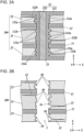
FIG. 1 is a sectional view of a printed wiring board. -
FIG. 2A is an enlarged view of a region including a through-hole inFIG. 1 . -
FIG. 2B is a view analogous toFIG. 2A except that the conductor is eliminated for convenience in describing the shape of the through-hole. -
FIG. 3 is a sectional view of a first recess, illustrating the shape of the first recess. -
FIG. 4 is an electron micrograph of first recesses. -
FIG. 5 is an electron micrograph of a through-hole 122 viewed in section. -
FIG. 6A, 6B ,7A, and 7B are sectional views and illustrate a method for manufacturing a printed wiring board. -
FIG. 8 is a table in which conditions for experiments conducted to verify the effects of Example are presented. -
FIG. 9 is an electron micrograph of an inner wall surface in Comparative Example 1. -
FIG. 10 is an electron micrograph of an inner wall surface in Comparative Example 2. - Embodiments will be described below with reference to the accompanying drawings. Constituent components are not drawn to scale, and the dimension ratios thereof do not fully correspond to the actual dimension ratios.
- Referring to
FIG. 1 , a printedwiring board 1 includes aconductor part 100 and aninsulating layer 200. Another perspective is that the printedwiring board 1 includes a core layer C and build-up layers B, which are provided on the front and back, respectively, of the core layer C. Theconductor part 100 and theinsulating layer 200 are partially included in the core layer C. Theconductor part 100 and theinsulating layer 200 are also partially included in the build-up layers B. - The following description about the orientation of each part of the printed
wiring board 1 is based on the XYZ Cartesian coordinate system, where Z denotes the thickness direction of the printedwiring board 1. Theinsulating layer 200 of the printedwiring board 1 has a first surface S1 and a second surface S2, which are parallel to the XY plane. The second surface S2 of theinsulating layer 200 is located opposite the first surface S1 of theinsulating layer 200.FIG. 1 illustrates a section perpendicular to the Y direction defined in relation to the printedwiring board 1. With regard to each of the layers constituting the printedwiring board 1, a surface oriented in the +Z direction may be hereinafter referred to as an upper surface, and a surface oriented in the -Z direction may be hereinafter referred to as a lower surface. - The core layer C includes a first
insulating layer 21 and a core conductor layers 11 (an inner layer circuit). The firstinsulating layer 21 is in the form of a flat plate. The firstinsulating layer 21 may be made of any desired insulating material. For example, the first insulatinglayer 21 is made of organic resin, such as polyphenylene ether (PPE) resin, polyphenylene oxide resin, or cyanate ester resin, or may be made of a mixture of two or more of these. - Specific examples of the material of the first insulating
layer 21 include: R-5725, R-5775, and R-5785 (manufactured by Panasonic Corporation); and DS-7409D and DS-7409DV (manufactured by Doosan Corporation). - A reinforcement material (base material) is preferably added to the organic resin that is to be used as the material of the first insulating
layer 21. For example, the reinforcement material is glass fiber, nonwoven glass fabric, nonwoven aramid fabric, aramid fiber, polyester fiber, or a combination of two or more of these. The firstinsulating layer 21 in the present embodiment contains glass fiber (cloth). - The first
insulating layer 21 also contains particles (an inorganic filler) dispersed therein. For example, the first insulatinglayer 21 contains particles of a substance such as aluminum hydroxide, silica, barium sulfate, talc, clay, glass, calcium carbonate, or titanium oxide. Each particle may be about 0.5 to 2 µm in diameter. The first insulatinglayer 21 may contain particles of a uniform diameter (size) or may have a predetermined particle size distribution. - The
core conductor layers 11 are predetermined wiring patterns extending over an upper surface and a lower surface, respectively, of the firstinsulating layer 21. Thecore conductor layers 11 are made of copper or any other material. - The build-up layers B are laid on an upper surface and a lower surface, respectively, of the core layer C.
- The build-up layers B include second
insulating layers 22 and aconductor 12. The secondinsulating layers 22 are each in the form of a flat plate. The first insulatinglayer 21 in the core layer C and the second insulatinglayers 22 in the respective build-up layers B constitute the insulatinglayer 200. The core conductor layers 11 in the core layer C and theconductor 12 in the build-up layers B constitute theconductor part 100. - The second insulating
layers 22 may be made of any desired insulating material. The first insulatinglayer 21 and the second insulatinglayers 22 may be made of the same material. For example, the second insulatinglayers 22 are made of polyphenylene ether (PPE) resin, polyphenylene oxide resin, cyanate ester resin, or a mixture of two or more of these. Specific examples of the material of the second insulatinglayers 22 include: R-5620, R-5670, R-5680 (manufactured by Panasonic Corporation); and DS-7409D and DS-7409DV (manufactured by Doosan Corporation). - A reinforcement material (base material) may be added to the organic resin that is to be used as the material of the second insulating layers 22. For example, the reinforcement material is glass fiber, nonwoven glass fabric, nonwoven aramid fabric, aramid fiber, polyester fiber, or a combination of two or more of these. As mentioned above, the first insulating
layer 21 contains glass fiber (cloth). The same goes for the second insulatinglayers 22 in the present embodiment. - The second insulating
layers 22 also contain particles (an inorganic filler) dispersed therein. The first insulatinglayer 21 and each of the second insulatinglayers 22 in the present embodiment contain particles of the same substance and within the same size range. The first insulatinglayer 21 and each of the second insulatinglayers 22 may contain particles of different materials and/or within different size ranges. - The
conductor 12 includes conductor layers 121, a through-hole 122, andvias 123. The through-hole 122 and thevias 123 each may serve as a connection conductor. The conductor is made of copper or any other material. - The conductor layers 121 are laid on the first surface S1 and the second surface S2, respectively, of the insulating
layer 200. Each of the conductor layers 121 is a wiring pattern and serves as a land for the through-hole 122 and the corresponding one of thevias 123. Each of theconductor layer 121 and the insulatinglayer 200 may be laid with copper foil provided therebetween; that is, each of theconductor layer 121 and the corresponding one of the second insulatinglayers 22 may be laid with copper foil provided therebetween. The copper foil is included in theconductor part 100. - The through-
hole 122 is provided on an inner wall surface of a cavity 3 (a pilot through-hole), which extends through the insulatinglayer 200. The through-hole 122 may be filled with aninsulator 23. The through-hole 122 is connected to the conductor layers 121 along the respective rims of thecavity 3 and is also connected to the core conductor layers 11 in the respective regions where the core conductor layers 11 are exposed at a surface defining thecavity 3. Thus, theconductor layer 121 on the first surface S1, theconductor layer 121 on the second surface, and the core conductor layers 11 are electrically connected to one another by the through-hole 122. - One of the
via 123 is fitted in the entirety of a cavity 4 (a pilot via) in the second insulatinglayer 22. Thecavity 4 extends from the first surface S1 to one of the core conductor layers 11. The via 123 is connected to the correspondingconductor layer 121 along the rim of thecavity 4 and is also connected to the correspondingcore conductor layer 11 at the bottom of thecavity 4. Thus, theconductor layer 121 and thecore conductor layer 11 are electrically connected to each other by thevia 123. As mentioned above, the via 123 illustrated inFIG. 1 is fitted in the entirety of thecavity 4. In another example, the via 123 is provided along an inner wall surface of thecavity 4 and is fitted in part of thecavity 4. That is, a surface of the via 123 may be recessed. - The following describes the through-
hole 122 in detail. - Referring to
FIG. 2B , the inner wall surface of thecavity 3 extending through the insulatinglayer 200 is denoted by 3a and includes first recesses 30. The first recesses 30 are formed when thecavity 3 undergoes a desmear process, which will be described later. - Referring to
FIG. 2A , the through-hole 122 includesprotrusions 122a, which are fitted in thefirst recesses 30 in thecavity 3. In other words, eachfirst recess 30 is fitted with the correspondingprotrusion 122a, which is part of the through-hole 122. With the through-hole 122 partially extending along theinner wall surface 3a, the portion on theinner wall surface 3a and eachprotrusion 122a of the through-hole 122 extend without a break therebetween. - The
protrusions 122a of the through-hole 122 provide enhanced adhesion between the through-hole 122 and the insulatinglayer 200. The enhanced adhesion reduces the possibility of cracking of the through-hole 122 and/or peeling of the plating on the through-hole 122 when the resin provided as the insulatinglayer 200 expands and contracts with temperature variations. - The through-
hole 122 and thecavity 3 inFIGs. 2A and 2B are illustrated in such a manner that uneven spots on their surfaces (theprotrusions 122a and the first recesses 30) look greater than they really are. In practical terms, part of theconductor 12 or, more specifically, the conductor layers 121 and the through-hole 122 each practically have a thickness of about 20 µm, whereas theprotrusions 122a and thefirst recesses 30 range in size from 0.1 to several micrometers. - Referring to
FIG. 2A , all of thefirst recesses 30 are fitted with therespective protrusions 122a. In some embodiments, some of thefirst recesses 30 are not fitted with theprotrusions 122a. - Referring to
FIGs. 3 and4 , thefirst recesses 30 each have aninner wall surface 30a, in which second recesses 300 are provided. The through-hole 122 is partially located in thesecond recesses 300; that is, theprotrusions 122a are partially located in thesecond recesses 300. Thus, each of theprotrusions 122a is shaped in conformance with the corresponding one of thefirst recesses 30 and inner walls of thesecond recesses 300. - It is not required that all of the
second recesses 300 be fitted with therespective protrusions 122a. In some embodiments, some of thefirst recesses 30 are not fitted with theprotrusions 122a. - Particles come off the insulating
layer 200 in the desmear process, which will be described later. The shape of each of thesecond recesses 300 is in conformity with part of the outer surface of the corresponding one of the particles. For example, particles coming off the insulatinglayer 200 are each in the form of a sphere, in which case the shape of the inner wall surface of each of thesecond recesses 300 left in the insulatinglayer 200 is in conformity with part of the corresponding one of the spheres. The insulatinglayer 200 in the present embodiment contains particles that are spherical or substantially spherical in shape. The second recesses 300 therefore each have a shape that is in conformity with part of the spherical shape or part of the substantially spherical shape. For example, the substantially spherical shape is a prolate spheroid, which is a solid generated by a half-revolution of an ellipse about its major axis. The situation in which particles come off the insulatinglayer 200 is herein also referred to as shedding. - Particles come off the insulating
layer 200 in the desmear process such that some of thefirst recesses 30 each have a shape that is in conformity with part of the outer surface of the corresponding particle. What is suggested here is that some of thefirst recesses 30 are traces that are left behind when particles come off the insulatinglayer 200. In a case where plasma treatment is employed in the desmear process, thefirst recesses 30 may be formed by erosion. - As illustrated in
FIG. 3 , D1 is greater than r1, which is one half of R1. Referring toFIG. 3 , D1 denotes the depth of thefirst recess 30, and R1 denotes the width of anopening 31 defined by thefirst recess 30 in theinner wall surface 3a of thecavity 3. The width R1 is the maximum width in a short transverse direction A2 of theopening 31 defined by the first recess 30 (see the lower part ofFIG. 4 ). The short transverse direction A2 is perpendicular to a longitudinal direction A1. The width (denoted by Rmax) in the longitudinal direction A1 is the maximum width of theopening 31 defined by thefirst recess 30. - It is not required that the inequality D1 > r1 hold for all of the first recesses 30.
- As illustrated in
FIG. 3 , D2 is greater than r2, which is one half of R1. Referring toFIG. 3 , D2 denotes the depth of at least one of thesecond recesses 300, and R2 denotes the width of anopening 301 defined by thesecond recess 300 in theinner wall surface 30a of thefirst recess 30. As mentioned above, the width R1 is the maximum width in the short transverse direction. Likewise, the width R2 is the maximum width in the short transverse direction of theopening 301. - It is not required that the inequality D2 > r2 hold for all of the
second recesses 300. - The
first recess 30 includes second recesses provided in aside face 30s, which is part of theinner wall surface 30a of thefirst recess 30. The second recesses concerned are also denoted by 300. In other words, some of thesecond recesses 300 are provided in theside face 30s of thefirst recess 30. Theside face 30s, which is part of theinner wall surface 30a, is inclined at an angle of 45° or more with respect to a plane in which theopening 31 defined by thefirst recess 30 is located. In some cases, not all thefirst recesses 30 include thesecond recesses 300 in their respective side faces 30s. - In the example described above with reference to
FIG. 3 , more than onesecond recess 300 is provided in theinner wall surface 30a of thefirst recess 30. However, the same does not necessarily hold true for all of thefirst recesses 30; that is, only onesecond recess 300 may be provided in theinner wall surface 30a. In some cases, not all thefirst recesses 30 include one or moresecond recesses 300 in their respectiveinner wall surfaces 30a. - Referring to
FIGs. 2A and5 , the through-hole 122 includesprojections 122b, which extend in a direction that forms an angle with theinner wall surface 3a of thecavity 3. Theprojections 122b are each in the form of a wedge inserted into the insulatinglayer 200, with one end of the wedge being located on a surface of the through-hole 122 that is closer than the other surface of the through-hole 122 to the insulatinglayer 200, that is, with one end of the wedge being located on a surface on theinner wall surface 3a of thecavity 3. Eachprojection 122b is about 3 to 10 µm long. Theprojections 122b are herein defined as portions of the through-hole 122 that project from theinner wall surface 3a into the insulatinglayer 200 and are not less than 3 µm long. The glass cloth contained in the insulatinglayer 200 is partially damaged when thecavity 3 is formed. The affected portions, which are hereinafter referred to as damaged portions 32 (seeFIG. 2B ), are impregnated with a plating solution and are thus formed into theprojections 122b. With the through-hole 122 partially extending along theinner wall surface 3 a, the portion on theinner wall surface 3a and eachprojection 122b of the through-hole 122 extend without a break therebetween. Theprojections 122b are located at intervals of two to three layers of glass cloth, with one ormore projections 122b being located in the same layer. Theprojections 122b further enhance the adhesion between the through-hole 122 and the insulatinglayer 200. - The through-
hole 122 is partially located in thefirst recesses 30 and thesecond recesses 300. As illustrated inFIG. 2A , eachprojection 122b and the portion in the correspondingfirst recess 30 extend without a break therebetween, and/or eachprojection 122b and the portion in at least one of thesecond recesses 300 extend without a break therebetween. - The following describes a method for manufacturing the printed
wiring board 1. - The method for manufacturing the printed
wiring board 1 according to the present embodiment includes first to fourth steps. The first step involves preparation of a substrate whose surface is covered with copper foil (not illustrated). Referring toFIG. 6A , the core conductor layers 11 are formed in the insulatinglayer 200 to serve as an inner layer circuit. - In the second step, the
cavity 3 is formed. Referring toFIG. 6B , thecavity 3 is a pilot through-hole extending from the first surface S1 of the insulatinglayer 200 to the second surface S2 of the insulatinglayer 200. The second step corresponds to a cavity forming step. For example, thecavity 3 is formed with a drill in such a way that processing can be added to the first insulatinglayer 21 and the second insulating layers 22. Alternatively, thecavity 3 may be formed with beams of laser light. - At the completion of the second step, a smear 90 (a resinous residue) is left on the inner wall surface of the
cavity 3. Thesmear 90 is produced at the time when the insulatinglayer 200 is processed. For example, thesmear 90 is caused by the melting of resin subjected to heat developed during the drilling process. - The glass cloth contained in the insulating
layer 200 is partially damaged in the second step. The affected portions in the insulatinglayer 200 are referred to as the damagedportions 32, as mentioned above. - The third step involves a desmear process by which the
smear 90 left on theinner wall surface 3a of thecavity 3 is removed. In the desmear process, plasma treatment (a plasma treatment step) is applied and is followed by ultrasonication (an ultrasonication step). - In the plasma treatment, at least one selected from the group consisting of N2, O2, and CF4 is used as an etching gas after being converted to plasma, and the
inner wall surface 3a of thecavity 3 is etched by using the copper foil on the surfaces of the insulatinglayer 200 as a mask. The plasma treatment is employed in such a way that thecavity 3 is exposed to plasma with an output power of 16 kW for 35 minutes and is then exposed to plasma with an output power of 15 kW for 40 minutes. Referring toFIG. 7A , thesmear 90 is removed by the plasma treatment. - The plasma treatment is followed by ultrasonication, where ultrasonic waves of a predetermined intensity are emitted to water or any other liquid in which the substrate is immersed. For example, ultrasonication is applied in such a way that ultrasonic vibrations with an output power of 1200 W and a frequency of 25 kHz are created for about 30 seconds without intermission. Particles exposed to view at the
inner wall surface 3a of thecavity 3 come off when subjected to ultrasonication. - The etching in the plasma treatment causes erosion of the
inner wall surface 3a, and the ultrasonication causes particles to come off theinner wall surface 3a. As illustrated inFIG. 7A , thefirst recesses 30 are formed in theinner wall surface 3a of thecavity 3 at the time of completion of the inner wall surface treatment in the third step. The second recesses 300 are also formed in the inner wall surfaces 30a of thefirst recesses 30 due to losses of particles. Particles come off such that the damagedportions 32 become adjacent to thefirst recesses 30 and/or thesecond recesses 300 with no gap between each damagedportion 32 and the adjacent recess. - In the fourth step, the
conductor 12 is formed. Referring toFIG. 7B , theconductor 12 including the conductor layers 121 and the through-hole 122 is formed by applying electrolytic panel plating to the substrate having thecavity 3 formed therein. The fourth step corresponds to a connection conductor forming step. Theconductor 12 formed in the fourth step is fitted in part of the cavity 3 (i.e., in the part extending through theinner wall surface 3a) to provide the through-hole 122. The first recesses 30 and thesecond recesses 300 in theinner wall surface 3a of thecavity 3 are filled in with theconductor 12. Theprotrusions 122a are formed accordingly. The damagedportions 32 are also filled in with theconductor 12 guided through thefirst recesses 30 and/or thesecond recesses 300 such that theprojections 122b are formed. - Subsequently, the
conductor 12 on the first surface S1 and the second surface S2 is patterned by a subtractive process and is formed into the conductor layers 121 (seeFIG. 1 ). The inner part of the through-hole 122 may be filled in with theinsulator 23. The printedwiring board 1 is obtained by the manufacturing method that has been described so far. - In some embodiments, the conductor layers 121 are formed by a modified semi-additive process (MSAP).
- The following describes an example of the printed
wiring board 1 according to the embodiment above. - Referring to
FIG. 8 , experiments were conducted to verify the effects of the example and involved desmear processes performed in different ways and/or under different conditions. In these experiments, substrates were subjected to the desmear processes after undergoing the first and second steps included in the manufacturing method mentioned above. - More specifically, the experiments are presented as Comparative Example 1, Comparative Example 2, and Example. The desmear process in Comparative Example 1 involved only chemical treatment in which an aqueous solution of potassium permanganate was used. The desmear process was performed using a 1 N (50 g/l) aqueous solution of potassium permanganate.
- The desmear process in Comparative Example 2 involved plasma treatment only. CF4 was used as an etching gas in the plasma treatment, in which the substrate was exposed to plasma with an output power of 16 kW for 35 minutes and was then exposed to plasma with an output power of 15 kW for 40 minutes.
- The desmear process in Example involved plasma treatment followed by ultrasonication. The plasma treatment was applied using CF4 as an etching gas. The substrate was exposed to plasma with an output power of 16 kW for 35 minutes and was then exposed to plasma with an output power of 15 kW for 40 minutes. The ultrasonication was applied in the following manner: ultrasonic waves were created by generating ultrasonic vibrations with an output power of 1200 W and a frequency of 25 kHz, and water in which the substrate was immersed was exposed to the ultrasonic waves for 30 seconds.
- For each of Comparative Example 1, Comparative Example 2, and Example, measurements were taken to determine the roughness (arithmetic mean roughness Ra) of the
inner wall surface 3a of thecavity 3 after the completion of the desmear process. The measurements obtained were as follows: (i) Ra in Comparative Example 1: 0 µm; (ii) Ra in Comparative Example 2: 0.5 µm; and (iii) Ra in Example: 1.0 µm. Theinner wall surface 3a was rougher in Example than in Comparative Example 1 and Comparative Example 2. This was due to the fact that particles came off theinner wall surface 3a in Example. - For each of Comparative Example 1, Comparative Example 2, and Example, the
inner wall surface 3a of thecavity 3 was photographed using a scanning electron microscope (SEM) after the completion of the desmear process. - As can be seen in
FIG. 9 , particles P were exposed at theinner wall surface 3a in Comparative Example 1. The experiment in which an aqueous solution of potassium permanganate was used in the desmear process revealed that particles P in the resin provided as the insulatinglayer 200 did not come off and remained buried in the insulatinglayer 200, which thus did not have recesses (traces of particles). - The
smear 90 was observed on theinner wall surface 3a. The desmear process in which an aqueous solution of potassium permanganate was used presumably produced little effect in removing a smear from the insulatinglayer 200 made mainly of a low dielectric constant material such as polyphenylene ether resin, polyphenylene oxide resin, or cyanate ester resin. - As can be seen in
FIG. 10 , thesmear 90 was not observed on theinner wall surface 3a in Comparative Example 2. The experiment revealed that the plasma treatment effectively removed thesmear 90. - Unfortunately, the particles P were exposed at the
inner wall surface 3a in Comparative Example 2. The experiment in which the desmear process involved only the plasma treatment revealed that particles P in the resin provided as the insulatinglayer 200 did not come off and remained buried in the insulatinglayer 200, which thus did not have recesses (traces of particles). - An electron micrograph of the
inner wall surface 3a in Example is presented inFIG. 4 . As can be seen inFIG. 4 , thefirst recesses 30 each including thesecond recesses 300 were formed in theinner wall surface 3a due to losses of the particles P. Example in which thefirst recesses 30 and thesecond recesses 300 were formed in theinner wall surface 3a of thecavity 3 revealed that theinner wall surface 3a was successfully roughened by the ultrasonication following the plasma treatment. - Following the completion of the desmear processes, Comparative Example 1, Comparative Example 2, and Example were each subjected to a heating test, after which the conductor 12 (the through-hole 122) on the
inner wall surface 3a was inspected for signs of peeling (see the rightmost column inFIG. 8 ). The substrates subjected to the heating test underwent six iterations of the reflow process (intended as a simulation for actual component mounting), in which each substrate was heated to 260°C. - After the completion of the heating test, signs of peeling of the
conductor 12 were observed in Comparative Example 1 and Comparative Example 2, whereas no sign of peeling of theconductor 12 was observed in Example (seeFIG. 8 ). The experiments revealed that enhanced adhesion between theconductor 12 and the insulatinglayer 200 was provided in Example, in which thefirst recesses 30 and thesecond recesses 300 were formed in theinner wall surface 3a of thecavity 3; that is, theinner wall surface 3a of thecavity 3 was roughened, which was due to shedding of particles with poor plating adhesion. - The printed
wiring board 1 according to the present embodiment includes the insulatinglayer 200 and theconductor part 100. The insulatinglayer 200 includes thecavity 3 perpendicular to the first surface S1 of the insulatinglayer 200. Theconductor part 100 includes the through-hole 122. The through-hole 122 is a connection conductor fitted in at least part of thecavity 3. Thecavity 3 includes thefirst recess 30. Thefirst recess 30 is provided in theinner wall surface 3a of thecavity 3. The through-hole 122 is partially fitted in thefirst recess 30. Thefirst recess 30 includes thesecond recess 300. Thesecond recess 300 is provided in theinner wall surface 30a of thefirst recess 30. The through-hole 122 is partially fitted in thesecond recess 300. - The
smear 90 produced at the time when the insulatinglayer 200 was processed may be removed by a known method, such as chemical treatment in which an aqueous solution of potassium permanganate solution is used. Unfortunately, the desmear process in which an aqueous solution of potassium permanganate is used produces little effect in removing thesmear 90 from the insulatinglayer 200 made mainly of a low dielectric constant material such as polyphenylene ether resin, polyphenylene oxide resin, or cyanate ester resin. This has been described above in relation to Comparative Example 1 with reference toFIG. 8 . Thesmear 90 is likely to cause faulty connection between the through-hole 122 and the core conductor layers 11. - The possibility of faulty connection may be addressed by the plasma treatment. The
smear 90 can be removed more effectively by the plasma treatment than would be possible by the chemical treatment in which an aqueous solution of potassium permanganate is used. Because of the nature of the plasma treatment, theinner wall surface 3a of thecavity 3 subjected to the plasma treatment tends to be less rough; that is, theinner wall surface 3a tends to have a small number of protrusions and recesses, and/or irregularities in theinner wall surface 3a tend to be less deep. Particles exposed at theinner wall surface 3a are hardly covered by plating. The resultant poor adhesion between theinner wall surface 3a of thecavity 3 and the through-hole 122 (the conductor 12) makes it difficult to attain thermal reliability. This can be understood from Comparative Example 2 (seeFIG. 8 ). More specifically, the insulating layer expands and contracts with temperature variations when undergoing, for example, a reflow process. As the insulatinglayer 200 expands and contracts perpendicularly to the first surface 1S, cracks can be developed in the through-hole 122, and/or the through-hole 122 can partially come off theinner wall surface 3a. - In the present embodiment, the
first recess 30 including thesecond recesses 300 is formed in theinner wall surface 3a of thecavity 3 and adds an extra surface area to theinner wall surface 3a. In this respect, the present embodiment has an advantage over the known art. The increased area of contact between the through-hole 122 (the conductor 12) and theinner wall surface 3a of thecavity 3 provides enhanced adhesion between the through-hole 122 and theinner wall surface 3a. The through-hole 122 can thus resist cracking and peeling when the insulatinglayer 200 expands and contracts with temperature variations. A high degree of thermal reliability is achieved accordingly. - Thus, the surface of the through-hole 122 (the surface closer to the cavity 3) is endowed with a suitable degree of roughness. The improvement obtained by the present embodiment is analogous to the development made in copper foil known as STD (standard copper foil). For example, RTF (reverse treated foil) is an advanced type of copper foil, and HVLP (hyper very low profile copper foil) is a further advanced type of copper foil. The adhesion between the through-
hole 122 and the insulatinglayer 200 is increased without degradation in radio-frequency signal transmission characteristics. - The
first recess 30 includes thesecond recesses 300 provided in theinner wall surface 30a of thefirst recess 30. The resultant increase in theinner wall surface 3a of thecavity 3 provides further enhanced adhesion between the through-hole 122 and theinner wall surface 3a of thecavity 3. - The depth D1 of at least one of the first recesses 30 is greater than the width r1, which is one half of the width R1 in the short transverse direction of the
opening 31 defined by thefirst recess 30 in theinner wall surface 3a of thecavity 3. This feature yields an increase in the area of contact between the through-hole 122 and the inner wall surface of thefirst recess 30, and theprotrusions 122a of the through-hole 122 are less likely to slip out of thefirst recess 30. The adhesion between the through-hole 122 and theinner wall surface 3a of thecavity 3 is further enhanced accordingly. - The depth D2 of at least one of the
second recesses 300 is greater than the width r2, which is one half of the width R2 in the short transverse direction of theopening 31 defined by thesecond recess 300 in theinner wall surface 30a of thefirst recess 30. This feature yields an increase in the area of contact between the through-hole 122 and the inner wall surface of thesecond recess 300, and portions of the through-hole 122 (eachprotrusion 122a) that are located within thesecond recess 300 are less likely to slip out of thesecond recess 300. The adhesion between the through-hole 122 and theinner wall surface 3a of thecavity 3 is further enhanced accordingly. - The
first recess 30 includes thesecond recess 300 provided in theside face 30s, which is part of theinner wall surface 30a of thefirst recess 30. In thesecond recess 300 provided in theside face 30s, theprotrusion 122a extends in a direction that forms an angle with the depth direction of thefirst recess 30. The portion in thesecond recess 300 provided in theside face 30s is hereinafter referred to as a side face filler portion. When a force is exerted in such a way as to withdraw theprotrusion 122a from thefirst recess 30 in its depth direction, the side face filler portion of theprotrusion 122a is caught in the inner wall surface of thesecond recess 300 such that theprotrusion 122a is hindered from slipping out of thefirst recess 30. The adhesion between the through-hole 122 and theinner wall surface 3a of thecavity 3 is further enhanced accordingly. - The insulating
layer 200 contains particles. Thesecond recess 300 has a shape that is in conformity with part of the outer surface of the corresponding one of the particles shed from the insulatinglayer 200. What is suggested here is that thesecond recess 300 is one of the traces that are left behind when the particles come off the insulatinglayer 200. The ultrasonication by which the particles come off the insulatinglayer 200 is simple and is all that is required to form thesecond recess 300. - The insulating
layer 200 contains particles. Thefirst recess 30 has a shape that is in conformity with part of the outer surface of the corresponding one of the particles shed from the insulatinglayer 200. What is suggested here is that thefirst recess 30 is one of the traces that are left behind when the particles come off the insulatinglayer 200. The ultrasonication by which the particles come off the insulatinglayer 200 is simple and is all that is required to form thefirst recess 30. - The through-
hole 122 includes theprojections 122b, which extend in the direction that forms an angle with theinner wall surface 3a of thecavity 3. The adhesion between the through-hole 122 and theinner wall surface 3a of thecavity 3 is further enhanced accordingly. - With the through-
hole 122 including a portion located in thefirst recess 30 and a portion located in thesecond recess 300, the portion in thefirst recess 30 and theprojection 122b extend without a break therebetween, and/or the portion in thesecond recess 300 and theprojection 122b extend without a break therebetween. Another perspective is that the damagedportions 32, which are located in the glass cloth and are to become theprojections 122b, are provided in such a manner as to meet thecavity 3 when particles exposed to view at theinner wall surface 3a of thecavity 3 come off. Thus, the damagedportions 32 are easily impregnated with a plating solution after the particles come off theinner wall surface 3a. The conductor 12 (the through-hole 122) including a larger number ofprojections 122b is formed accordingly. - The connection conductor is the through-
hole 122, which extends through the printedwiring board 1. The conductor layers 121 on both sides of the insulatinglayer 200 are thus electrically connected to the core conductor layers 11 in the insulatinglayer 200. The adhesion between the through-hole 122 and theinner wall surface 3a of thecavity 3 is enhanced by thefirst recess 30 and thesecond recess 300, leading to increased reliability of the connection. - The insulating
layer 200 contains at least one selected from the group consisting of polyphenylene ether resin, polyphenylene oxide resin, and cyanate ester resin. This composition makes it difficult to remove thesmear 90 from the insulatinglayer 200 with an aqueous solution of potassium permanganate. As a workaround, the embodiment above involves the desmear process including both the plasma treatment and the ultrasonication. The desmear process in the embodiment enables removal of thesmear 90 and increases the adhesion between the through-hole 122 and theinner wall surface 3a of thecavity 3. - The method for manufacturing the printed
wiring board 1 according to the present embodiment includes the cavity forming step, the plasma treatment step, the ultrasonication step, and a connection conductor forming step. In the cavity forming step, thecavity 3 perpendicular to the first surface S1 of the insulatinglayer 200 containing particles is formed. In the plasma treatment step, thesmear 90 produced in the insulatinglayer 200 in the cavity forming step is removed by plasma treatment. In the ultrasonication step, thesecond recess 300 is formed in theinner wall surface 30a of thefirst recess 30 in theinner wall surface 3a of thecavity 3 by ultrasonication after the plasma treatment step in such a manner that the particles contained in the insulatinglayer 200 and exposed to view at theinner wall surface 3a of thecavity 3 come off the insulatinglayer 200. In the connection conductor forming step, the through-hole 122 is formed to be fitted in thefirst recess 30, thesecond recess 300, and at least part of thecavity 3. The method, by which thefirst recess 30 including thesecond recess 300 provided in theinner wall surface 3a of thecavity 3, adds an extra surface area to theinner wall surface 3a. In this respect, the method has an advantage over the known art. The increased area of contact between the through-hole 122 (the conductor 12) and theinner wall surface 3a of thecavity 3 and the shedding of particles with poor plating adhesion provide enhanced adhesion between the through-hole 122 and theinner wall surface 3a. The through-hole 122 can thus resist cracking and peeling when the insulatinglayer 200 expands and contracts with temperature variations. A high degree of thermal reliability is achieved accordingly. - The
smear 90 is effectively removed by the plasma treatment in which at least one selected from the group consisting of N2 gas, O2 gas, and CF4 gas is used. - The embodiment above is presented as an example, and various changes may be made to the embodiment.
- The
first recess 30 and thesecond recess 300 in the embodiment above are formed in theinner wall surface 3a of the cavity 3 (a pilot through-hole) on which the through-hole 122 (the connection conductor) is provided. In some embodiments, thefirst recess 30 and thesecond recess 300 are formed in the inner wall surface of the cavity 4 (a pilot blind via) of each via 123 (the connection conductor). - The conditions for the plasma treatment and the conditions for the ultrasonication in the embodiment above are presented as examples and may be adjusted as appropriate depending on, for example, the material and size of the insulating
layer 200 and the material and size of the particles contained in the insulatinglayer 200. - The printed
wiring board 1 in the embodiment above includes the through-hole 122 and thevia 123. In some embodiments, the printedwiring board 1 includes the through-hole 122 or the via 123 only. - Two or more build-up layers B may be laid on each surface of the core layer C. The build-up layers B are optional. That is, the printed
wiring board 1 may be essentially the core layer C. - The core layer C may include two or more first insulating layers 21. The build-up layers B each may include two or more second insulating layers 22. Only one surface of the core layer C may be overlaid with the build-up layer B.
- The printed
wiring board 1 may include only oneconductor layer 121 located on one surface of the printedwiring board 1. - The details (e.g., features, structures, positional relationships, and shapes) described above in relation to the embodiment may be changed as appropriate within a range not departing from the spirit of the disclosure. The features, structures, positional relationships, and shapes described above in relation to the embodiment may be employed in combination as appropriate within a range not departing from the spirit of the disclosure.
- The present disclosure is applicable to a printed wiring board and a method for manufacturing a printed circuit board.
-
- 1 printed wiring board
- 3, 4 cavity
- 3 a inner wall surface
- 100 conductor part
- 11 core conductor layer
- 12 conductor
- 121 conductor layer
- 122 through-hole (connection conductor)
- 122a protrusion
- 122b projection
- 123 via (connection conductor)
- 200 insulating layer
- 21 first insulating layer
- 22 second insulating layer
- 23 insulator
- 30 first recess
- 30a inner wall surface
- 30s side face
- 31 opening
- 32 damaged portion
- 300 second recess
- 301 opening
- 90 smear
- A1 longitudinal direction
- A2 short transverse direction
- B build-up layer
- C core layer
- P particle
Claims (13)
- A printed wiring board, comprising:an insulating layer; anda conductor part, whereinthe insulating layer comprises a cavity perpendicular to a first surface of the insulating layer,the conductor part comprises a connection conductor fitted in at least part of the cavity,the cavity comprises a first recess provided in an inner wall surface of the cavity, the connection conductor being partially fitted in the first recess, andthe first recess comprises a second recess provided in an inner wall surface of the first recess, the connection conductor being partially fitted in the second recess.
- The printed wiring board according to claim 1, wherein the first recess comprises a plurality of the second recesses provided in the inner wall surface of the first recess.
- The printed wiring board according to claim 1 or 2, wherein a depth of the first recess is greater than one half of a width in a short transverse direction of an opening defined by the first recess in the inner wall surface of the cavity.
- The printed wiring board according to any one of claims 1 to 3, wherein a depth of the second recess is greater than one half of a width in a short transverse direction of an opening defined by the second recess in the inner wall surface of the first recess.
- The printed wiring board according to any one of claims 1 to 4, wherein the first recess comprises the second recess provided in a side face being part of the inner wall surface of the first recess.
- The printed wiring board according to any one of claims 1 to 5, whereinthe insulating layer contains particles, andthe second recess has a shape being in conformity with part of an outer surface of a corresponding one of the particles shed from the insulating layer.
- The printed wiring board according to any one of claims 1 to 6, whereinthe insulating layer contains particles, andthe first recess has a shape being in conformity with part of an outer surface of a corresponding one of the particles shed from the insulating layer.
- The printed wiring board according to any one of claims 1 to 7, wherein the connection conductor includes a projection extending in a direction forming an angle with the inner wall surface of the cavity.
- The printed wiring board according to claim 8, wherein with the connection conductor comprising a portion located in the first recess and a portion located in the second recess, the portion in the first recess and the projection extend without a break therebetween, and/or the portion in the second recess and the projection extend without a break therebetween.
- The printed wiring board according to any one of claims 1 to 9, wherein the connection conductor is a through-hole extending through the printed wiring board.
- The printed wiring board according to any one of claims 1 to 10, wherein the insulating layer contains at least one selected from the group consisting of polyphenylene ether resin, polyphenylene oxide resin, and cyanate ester resin.
- A method for manufacturing a printed wiring board, the method comprising:a cavity forming step in which a cavity perpendicular to a first surface of an insulating layer containing particles is formed;a plasma treatment step in which a smear produced in the insulating layer in the cavity forming step is removed by plasma treatment;an ultrasonication step in which a second recess is formed in an inner wall surface of a first recess in an inner wall surface of the cavity by ultrasonication after the plasma treatment step in such a manner that the particles contained in the insulating layer and exposed to view at the inner wall surface of the cavity come off the insulating layer; anda connection conductor forming step in which a connection conductor is formed to be fitted in the first recess, the second recess, and at least part of the cavity.
- The method for manufacturing a printed wiring board according to claim 12, wherein the plasma treatment is conducted by using at least one selected from the group consisting of N2 gas, O2 gas, and CF4 gas.
Applications Claiming Priority (2)
| Application Number | Priority Date | Filing Date | Title |
|---|---|---|---|
| JP2020059288 | 2020-03-30 | ||
| PCT/JP2021/012542 WO2021200538A1 (en) | 2020-03-30 | 2021-03-25 | Printed wiring board and method for manufacturing printed wiring board |
Publications (2)
| Publication Number | Publication Date |
|---|---|
| EP4132236A1 true EP4132236A1 (en) | 2023-02-08 |
| EP4132236A4 EP4132236A4 (en) | 2024-05-01 |
Family
ID=77929181
Family Applications (1)
| Application Number | Title | Priority Date | Filing Date |
|---|---|---|---|
| EP21781971.3A Withdrawn EP4132236A4 (en) | 2020-03-30 | 2021-03-25 | PRINTED CIRCUIT BOARD AND METHOD FOR MANUFACTURING A PRINTED CIRCUIT BOARD |
Country Status (5)
| Country | Link |
|---|---|
| US (1) | US12484155B2 (en) |
| EP (1) | EP4132236A4 (en) |
| JP (1) | JP7364787B2 (en) |
| CN (1) | CN115336401A (en) |
| WO (1) | WO2021200538A1 (en) |
Family Cites Families (16)
| Publication number | Priority date | Publication date | Assignee | Title |
|---|---|---|---|---|
| JPH05235544A (en) | 1992-02-19 | 1993-09-10 | Ibiden Co Ltd | Manufacture of composite printed circuit board |
| JP3766125B2 (en) | 1995-10-16 | 2006-04-12 | イビデン株式会社 | Multilayer printed wiring board and manufacturing method thereof |
| JP3050807B2 (en) * | 1996-06-19 | 2000-06-12 | イビデン株式会社 | Multilayer printed wiring board |
| KR100906931B1 (en) * | 1998-02-26 | 2009-07-10 | 이비덴 가부시키가이샤 | Multilayer printed wiring board having filled-via structure |
| JP4724547B2 (en) | 2005-12-08 | 2011-07-13 | 新光電気工業株式会社 | Cleaning method of resin layer surface |
| JP4303282B2 (en) | 2006-12-22 | 2009-07-29 | Tdk株式会社 | Wiring structure of printed wiring board and method for forming the same |
| US8925192B2 (en) * | 2009-06-09 | 2015-01-06 | Ibiden Co., Ltd. | Printed wiring board and method for manufacturing the same |
| US8581104B2 (en) * | 2010-03-31 | 2013-11-12 | Ibiden Co., Ltd. | Wiring board and method for manufacturing the same |
| CN102413641A (en) | 2010-07-22 | 2012-04-11 | 日本特殊陶业株式会社 | Multilayer wiring board and manufacturing method thereof |
| CN103069932B (en) * | 2010-08-31 | 2015-10-21 | 京瓷株式会社 | Wiring substrate and its mounting structure |
| WO2012042846A1 (en) * | 2010-09-27 | 2012-04-05 | 太陽ホールディングス株式会社 | Method for forming solder resist |
| JP5892157B2 (en) * | 2011-03-25 | 2016-03-23 | 住友ベークライト株式会社 | Printed circuit board, method for manufacturing printed circuit board, and semiconductor device |
| JP2014127623A (en) * | 2012-12-27 | 2014-07-07 | Shinko Electric Ind Co Ltd | Wiring board and method of manufacturing the same |
| CN107211542B (en) * | 2014-11-28 | 2020-11-24 | 英特尔公司 | Desmearing treatment method and manufacturing method of multilayer printed wiring board |
| JP6643956B2 (en) | 2016-01-25 | 2020-02-12 | 京セラ株式会社 | Printed wiring board and manufacturing method thereof |
| JP2018182229A (en) * | 2017-04-20 | 2018-11-15 | 富士通株式会社 | Substrate and method of manufacturing substrate |
-
2021
- 2021-03-25 JP JP2022512065A patent/JP7364787B2/en active Active
- 2021-03-25 CN CN202180023544.8A patent/CN115336401A/en active Pending
- 2021-03-25 WO PCT/JP2021/012542 patent/WO2021200538A1/en not_active Ceased
- 2021-03-25 EP EP21781971.3A patent/EP4132236A4/en not_active Withdrawn
- 2021-03-25 US US17/912,619 patent/US12484155B2/en active Active
Also Published As
| Publication number | Publication date |
|---|---|
| JPWO2021200538A1 (en) | 2021-10-07 |
| JP7364787B2 (en) | 2023-10-18 |
| EP4132236A4 (en) | 2024-05-01 |
| US20230319999A1 (en) | 2023-10-05 |
| WO2021200538A1 (en) | 2021-10-07 |
| US12484155B2 (en) | 2025-11-25 |
| CN115336401A (en) | 2022-11-11 |
Similar Documents
| Publication | Publication Date | Title |
|---|---|---|
| JP5568618B2 (en) | Method of manufacturing a circuit carrier and use of the method | |
| CN101352109B (en) | Printed wiring board and method for manufacturing the same | |
| US6618940B2 (en) | Fine pitch circuitization with filled plated through holes | |
| TWM254863U (en) | Multi-layer wiring board | |
| KR20030063140A (en) | Printed circuit board and manufacturing method therefor | |
| CN100591192C (en) | Radiant heat printed circuit board and manufacturing method thereof | |
| CN1194590C (en) | Method for manufacturing printed wiring board | |
| US12484155B2 (en) | Printed wiring board and method for manufacturing printed wiring board | |
| JP2000036660A (en) | Manufacture of build-up multilayer interconnection board | |
| KR20030016515A (en) | method for producing build-up multi-layer printed circuit board using a via filling | |
| JP4791648B2 (en) | Non-through hole processing method for printed wiring board | |
| KR100274662B1 (en) | Method for manufacturing interlayer vias of multilayer printed circuit boards | |
| JP2000036659A (en) | Manufacture of build-up multilayer interconnection board | |
| JP2000036661A (en) | Manufacture of build-up multilayer interconnection board | |
| GB2203290A (en) | Manufacture of printed circuit boards | |
| JP2000216521A (en) | Wiring board manufacturing method and wiring board using the same | |
| JP2000036662A (en) | Manufacture of build-up multilayer interconnection board | |
| CN223744978U (en) | Inner layer board of circuit board and circuit board | |
| JP2003008222A (en) | High-density multilayer build-up wiring board and method of manufacturing the same | |
| JP3881528B2 (en) | Wiring board and manufacturing method thereof | |
| JPH06244528A (en) | Method for manufacturing printed wiring board | |
| JP2002359468A (en) | Multilayer printed wiring board having filled via structure and method of manufacturing the same | |
| JP2002359467A (en) | Multilayer printed wiring board having filled via structure and method of manufacturing the same | |
| JP2003298207A (en) | Manufacturing method of double-side circuit board | |
| JPH07297519A (en) | Manufacture of wiring board |
Legal Events
| Date | Code | Title | Description |
|---|---|---|---|
| STAA | Information on the status of an ep patent application or granted ep patent |
Free format text: STATUS: THE INTERNATIONAL PUBLICATION HAS BEEN MADE |
|
| PUAI | Public reference made under article 153(3) epc to a published international application that has entered the european phase |
Free format text: ORIGINAL CODE: 0009012 |
|
| STAA | Information on the status of an ep patent application or granted ep patent |
Free format text: STATUS: REQUEST FOR EXAMINATION WAS MADE |
|
| 17P | Request for examination filed |
Effective date: 20220919 |
|
| AK | Designated contracting states |
Kind code of ref document: A1 Designated state(s): AL AT BE BG CH CY CZ DE DK EE ES FI FR GB GR HR HU IE IS IT LI LT LU LV MC MK MT NL NO PL PT RO RS SE SI SK SM TR |
|
| P01 | Opt-out of the competence of the unified patent court (upc) registered |
Effective date: 20230505 |
|
| DAV | Request for validation of the european patent (deleted) | ||
| DAX | Request for extension of the european patent (deleted) | ||
| REG | Reference to a national code |
Ref country code: DE Ref legal event code: R079 Free format text: PREVIOUS MAIN CLASS: H05K0003420000 Ipc: H05K0003000000 |
|
| A4 | Supplementary search report drawn up and despatched |
Effective date: 20240402 |
|
| RIC1 | Information provided on ipc code assigned before grant |
Ipc: H05K 3/42 20060101ALN20240325BHEP Ipc: H05K 3/00 20060101AFI20240325BHEP |
|
| STAA | Information on the status of an ep patent application or granted ep patent |
Free format text: STATUS: THE APPLICATION HAS BEEN WITHDRAWN |
|
| 18W | Application withdrawn |
Effective date: 20251219 |