EP4131418A1 - Buffer region variable doping structure used for overvoltage breakdown function, and semiconductor device - Google Patents
Buffer region variable doping structure used for overvoltage breakdown function, and semiconductor device Download PDFInfo
- Publication number
- EP4131418A1 EP4131418A1 EP20927940.5A EP20927940A EP4131418A1 EP 4131418 A1 EP4131418 A1 EP 4131418A1 EP 20927940 A EP20927940 A EP 20927940A EP 4131418 A1 EP4131418 A1 EP 4131418A1
- Authority
- EP
- European Patent Office
- Prior art keywords
- region
- dopant
- dopant region
- buffer
- doping structure
- Prior art date
- Legal status (The legal status is an assumption and is not a legal conclusion. Google has not performed a legal analysis and makes no representation as to the accuracy of the status listed.)
- Pending
Links
Images




Classifications
-
- H—ELECTRICITY
- H10—SEMICONDUCTOR DEVICES; ELECTRIC SOLID-STATE DEVICES NOT OTHERWISE PROVIDED FOR
- H10D—INORGANIC ELECTRIC SEMICONDUCTOR DEVICES
- H10D62/00—Semiconductor bodies, or regions thereof, of devices having potential barriers
- H10D62/10—Shapes, relative sizes or dispositions of the regions of the semiconductor bodies; Shapes of the semiconductor bodies
- H10D62/124—Shapes, relative sizes or dispositions of the regions of semiconductor bodies or of junctions between the regions
-
- H—ELECTRICITY
- H10—SEMICONDUCTOR DEVICES; ELECTRIC SOLID-STATE DEVICES NOT OTHERWISE PROVIDED FOR
- H10D—INORGANIC ELECTRIC SEMICONDUCTOR DEVICES
- H10D18/00—Thyristors
- H10D18/60—Gate-turn-off devices
-
- H—ELECTRICITY
- H10—SEMICONDUCTOR DEVICES; ELECTRIC SOLID-STATE DEVICES NOT OTHERWISE PROVIDED FOR
- H10D—INORGANIC ELECTRIC SEMICONDUCTOR DEVICES
- H10D12/00—Bipolar devices controlled by the field effect, e.g. insulated-gate bipolar transistors [IGBT]
- H10D12/411—Insulated-gate bipolar transistors [IGBT]
- H10D12/441—Vertical IGBTs
-
- H—ELECTRICITY
- H10—SEMICONDUCTOR DEVICES; ELECTRIC SOLID-STATE DEVICES NOT OTHERWISE PROVIDED FOR
- H10D—INORGANIC ELECTRIC SEMICONDUCTOR DEVICES
- H10D12/00—Bipolar devices controlled by the field effect, e.g. insulated-gate bipolar transistors [IGBT]
- H10D12/411—Insulated-gate bipolar transistors [IGBT]
- H10D12/441—Vertical IGBTs
- H10D12/491—Vertical IGBTs having both emitter contacts and collector contacts in the same substrate side
-
- H—ELECTRICITY
- H10—SEMICONDUCTOR DEVICES; ELECTRIC SOLID-STATE DEVICES NOT OTHERWISE PROVIDED FOR
- H10D—INORGANIC ELECTRIC SEMICONDUCTOR DEVICES
- H10D18/00—Thyristors
- H10D18/211—Thyristors having built-in localised breakdown or breakover regions, e.g. self-protected against destructive spontaneous firing
-
- H—ELECTRICITY
- H10—SEMICONDUCTOR DEVICES; ELECTRIC SOLID-STATE DEVICES NOT OTHERWISE PROVIDED FOR
- H10D—INORGANIC ELECTRIC SEMICONDUCTOR DEVICES
- H10D18/00—Thyristors
- H10D18/40—Thyristors with turn-on by field effect
-
- H—ELECTRICITY
- H10—SEMICONDUCTOR DEVICES; ELECTRIC SOLID-STATE DEVICES NOT OTHERWISE PROVIDED FOR
- H10D—INORGANIC ELECTRIC SEMICONDUCTOR DEVICES
- H10D62/00—Semiconductor bodies, or regions thereof, of devices having potential barriers
- H10D62/10—Shapes, relative sizes or dispositions of the regions of the semiconductor bodies; Shapes of the semiconductor bodies
- H10D62/13—Semiconductor regions connected to electrodes carrying current to be rectified, amplified or switched, e.g. source or drain regions
- H10D62/141—Anode or cathode regions of thyristors; Collector or emitter regions of gated bipolar-mode devices, e.g. of IGBTs
- H10D62/142—Anode regions of thyristors or collector regions of gated bipolar-mode devices
-
- H—ELECTRICITY
- H10—SEMICONDUCTOR DEVICES; ELECTRIC SOLID-STATE DEVICES NOT OTHERWISE PROVIDED FOR
- H10D—INORGANIC ELECTRIC SEMICONDUCTOR DEVICES
- H10D62/00—Semiconductor bodies, or regions thereof, of devices having potential barriers
- H10D62/60—Impurity distributions or concentrations
-
- H—ELECTRICITY
- H10—SEMICONDUCTOR DEVICES; ELECTRIC SOLID-STATE DEVICES NOT OTHERWISE PROVIDED FOR
- H10D—INORGANIC ELECTRIC SEMICONDUCTOR DEVICES
- H10D62/00—Semiconductor bodies, or regions thereof, of devices having potential barriers
- H10D62/10—Shapes, relative sizes or dispositions of the regions of the semiconductor bodies; Shapes of the semiconductor bodies
- H10D62/17—Semiconductor regions connected to electrodes not carrying current to be rectified, amplified or switched, e.g. channel regions
- H10D62/192—Base regions of thyristors
- H10D62/199—Anode base regions of thyristors
Definitions
- the present invention relates to the field of semiconductor devices, and in particular to a buffer-region variable doping structure for an overvoltage breakdown function and a semiconductor device.
- An IGCT device is a new-generation current-controlled device developed on the basis of GTO.
- a GCT chip is made through the transparent anode technology and designed with buffer layers, which reduces the trigger current level and on-voltage drop of the device.
- the IGCT adopts the integrated drive circuit, optimizes the circuit layout and the structure of housing package, and reduces the parasitic parameters of commutation loop to the level of nanohenry, so that the device can commutate all current from cathode electrode to gate electrode in a short period in the turn-off process, and then the PNP transistor can be turned off naturally.
- FIG. 1 is a schematic diagram of an existing GCT chip structure.
- the J2 junction when statically blocking or dynamically turning off, the J2 junction withstands the voltage above the kV level between a cathode and an anode.
- the n-type drift region is usually made into a low-doped concentration region from the original silicon single crystal. In this case, the voltage mainly drops in the n-type drift region.
- the change rate of the electric field is proportional to the doping concentration, that is, a lower doping concentration offers a higher blocking voltage with properly designed structure.
- Semiconductor devices show unique advantages in the fields of large-capacity flexible power transmission due to their high blocking voltage capabilities, high controllable current levels, low conduction loss, high reliability, and low costs.
- Existing semiconductor devices include IGBT, IEGT, IGCT, ETO MCT, and the like.
- FIG. 1 is a cross-sectional schematic diagram of a conventional silicon-based GCT unit.
- the forward withstand voltage is mainly borne by the J2 junction marked in the figure.
- FIG. 2 is a schematic diagram of conventional GCT edge grinding.
- the direct use of traditional structures for overvoltage breakdown mainly faces two problems: limited by factors such as process stability and contamination, the breakdown voltage and leakage current levels of the devices after the edge passivation treatment usually have a dispersion, and are difficult to test and screen; and If the overvoltage breakdown occurs and the system energy is large, because the weak point of voltage withstanding is at the edge, the influx of inrush current is likely to cause the rupture of the device shell structure, threatening the safe operation of the entire valve. Therefore, as for the IGCT, IGBT, SGTO, and the like, the weak points of their breakdown voltages are all at the edge. In addition, the edge of the IGCT is handled by grinding the corner, and the edges of the IGBT and other devices are handled through technologies such as junction terminal expansion. However, the two edge handling manners cause unstable and uncontrollable problems.
- FIG. 3 is a schematic structural diagram of a thyristor BOD.
- the BOD (break over diode) structure shown in FIG. 3 is usually configured to protect the overvoltage.
- the BOD structure first generates a relatively strong leakage current, and the lateral voltage raised by the leakage current triggers the electron emission at the amplifying gate, thereby conducting the thyristor device and avoiding failure.
- the essence of the BOD structure is to create a weak point for avalanche breakdown in the device body (usually at the center), thereby ensuring that the device at the BOD structure is broken down stably under a specific voltage.
- the avalanche coefficient is greatly affected by a temperature, there may be about 10% or higher variation in the protection threshold value at different temperatures with an identical doping structure.
- this technology is applied to a semiconductor device, it is difficult to use the BOD structure to reliably protect the overvoltage of the device due to the limitations of the device structure and process implementation.
- the present invention provides a buffer-region variable doping structure for an overvoltage breakdown function.
- the buffer-region variable doping structure is disposed in a semiconductor device, where when the semiconductor device withstands a breakdown voltage, the buffer-region variable doping structure withstands an electric field generated by the semiconductor device, such that the electric field punches through the buffer-region variable doping structure.
- the buffer-region variable doping structure includes a first dopant region A and a second dopant region B, where the first dopant region A and the second dopant region B are attached up and down, and when the semiconductor device withstands the breakdown voltage, the first dopant region A and the second dopant region B generate the electric field.
- the buffer-region variable doping structure further includes a second dopant region C and a second dopant region D, where the second dopant region C is connected to the second dopant region D, the second dopant region C and the second dopant region D are in a same layer and are both attached to the second dopant region B up and down, and a total dopant dose of the second dopant region D is smaller than a total dopant dose of the second dopant region C, when the second dopant region C and the second dopant region D withstand the electric field, such that the electric field punches through the second dopant region D.
- the buffer-region variable doping structure further includes a second dopant region C, a second dopant region D, and a first dopant region E, where the second dopant region C and the first dopant region E are connected to the second dopant region D, the second dopant region C and the second dopant region D are attached to the second dopant region B up and down, the first dopant region E and the second dopant region C are attached up and down, and a total dopant dose of the second dopant region D is smaller than a total dopant dose of the second dopant region C, when the second dopant region C and the second dopant region D withstand the electric field, such that the electric field punches through the second dopant region D.
- the buffer-region variable doping structure further includes a second dopant region C, a second dopant region D, a first dopant region E, and a first dopant region F, where the second dopant region C is connected to the second dopant region D, the first dopant region E is connected to the first dopant region F, the second dopant region C and the second dopant region D are attached to the second dopant region B up and down, the first dopant region E and the second dopant region C are attached up and down, the first dopant region F and the second dopant region D are attached up and down, and a total dopant dose of the second dopant region D is smaller than a total dopant dose of the second dopant region C, when the second dopant region C and the second dopant region D withstand the electric field, such that the electric field punches through the second dopant region D.
- a net total quantity of the dopant per unit area of the first dopant region F is smaller than each of the net total quantities of the dopants per unit area of the other dopant regions.
- the net total quantity of the dopant per unit area of the first dopant region F makes the buffer-region variable doping structure under static blocking have a hole emission efficiency equal to or lower than that of another dopant region.
- the present invention provides a semiconductor device, including the buffer-region variable doping structure described above, where when the semiconductor device withstands a breakdown voltage, the buffer-region variable doping structure withstands an electric field generated by the semiconductor device, such that the electric field punches through the buffer-region variable doping structure.
- the semiconductor device is one of IGCT, GTO, SGTO, IGBT, IEGT, MCT, and ETO.
- the present invention has the following effects: Overvoltage self-destruction is performed on the buffer-region variable doping structure and a semiconductor device having the same in the present invention according to the local punch-through principle, with the advantages of good temperature stability, easy process realization, and good voltage consistency. Further, because the punch-through point is located in the body, after the self-destruction, the device can usually be remained in a reliable short-circuit state for a long time.
- the buffer-region variable doping structure for an overvoltage breakdown function in the present invention is disposed in a semiconductor device.
- the buffer-region variable doping structure withstands an electric field generated by the semiconductor device, such that the electric field punches through the buffer-region variable doping structure.
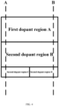
- FIG. 4 is a schematic diagram of a buffer-region variable doping structure according to a first embodiment of the present invention.
- the buffer-region variable doping structure for an overvoltage breakdown function of the present invention includes a first dopant region A and a second dopant region B, the first dopant region A and the second dopant region B are attached up and down, and when the semiconductor device withstands the breakdown voltage, the first dopant region A and the second dopant region B generate the electric field.
- the first dopant region A and the second dopant region B are each a p-type dopant or an n-type dopant. Specifically, if the first dopant region A is the p-type dopant, the second dopant region B is the n-type dopant, and vice versa.
- the buffer-region variable doping structure further includes a second dopant region C and a second dopant region D, where the second dopant region C is connected to the second dopant region D, the second dopant region C and the second dopant region D are in a same layer and are both attached to the second dopant region B up and down, and when the second dopant region C and the second dopant region D withstand the electric field, a total dopant dose of the second dopant region D is smaller than a total dopant dose of the second dopant region C, such that the electric field punches through the second dopant region D.
- the buffer-region variable doping structure of the present invention includes a second dopant region C and a second dopant region D.
- the second dopant region C and the second dopant region D both withstand the electric field generated by the semiconductor device.
- the total dopant dose of the second dopant region D is smaller than that of the second dopant region C. Therefore, the electric field does not punch through the second dopant region C, but the second dopant region D.
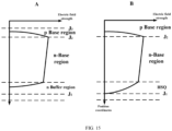
- FIG. 5 is a schematic distribution diagram of electric fields in various places of the buffer-region variable doping structure in FIG. 4 under a state of withstanding a designed breakdown voltage.
- the doping of the second dopant region D needs to ensure that when the semiconductor device statically withstands the designed breakdown voltage value, the electric field applied between the first dopant region A and the second dopant region B punches through the second dopant region D exactly.
- the electric field distribution under the critical state is shown in FIG. 5 .
- the total dopant dose of the second dopant region D may be designed with reference to the foregoing formula. Therefore, the design of the second dopant region D can not only reduce the doping concentration while ensuring the junction depth, but also reduce the junction depth and the doping concentration at the same time.
- FIG. 6 is a schematic diagram of a buffer-region variable doping structure according to a second embodiment of the present invention.
- the buffer-region variable doping structure in FIG. 6 and the one in FIG. 4 are roughly the same. Therefore, only the different parts are described below.
- the buffer-region variable doping structure further includes a second dopant region C, a second dopant region D, a first dopant region E, and a first dopant region F, where the second dopant region C is connected to the second dopant region D, the first dopant region E is connected to the first dopant region F, the second dopant region C and the second dopant region D are attached to the second dopant region B up and down, the first dopant region E and the second dopant region C are attached up and down, the first dopant region F and the second dopant region D are attached up and down, and when the second dopant region C and the second dopant region D withstand the electric field, a total dopant dose of the second dopant region D is smaller than a total dopant dose of the second dopant region C, such that the electric field punches through the second dopant region D.
- the net total quantity of the dopant per unit area of the first dopant region F makes the buffer-region variable doping structure under static blocking have a hole emission efficiency equal to or lower than that of another dopant region.
- a first dopant region E for carrier emission including a first dopant of a higher concentration.
- a first dopant region F with a small-dose dopant is disposed under the second dopant region D.
- the first dopant region F may be lower than the remaining regions. Specifically, the first dopant region F may be not doped with the first dopant.
- a net total quantity of the dopant per unit area of the first dopant region F is smaller than each of the net total quantities of the dopants per unit area of the other dopant regions.
- FIG. 7 is a schematic diagram of a buffer-region variable doping structure according to a third embodiment of the present invention.
- the buffer-region variable doping structure in FIG. 7 and the one in FIG. 6 are roughly the same. Therefore, only the different parts are described below.
- the buffer-region variable doping structure further includes a second dopant region C, a second dopant region D, and a first dopant region E, where the second dopant region C and the first dopant region E are connected to the second dopant region D, the second dopant region C and the second dopant region D are attached to the second dopant region B up and down, the first dopant region E and the second dopant region C are attached up and down, and when the second dopant region C and the second dopant region D withstand the electric field, a total dopant dose of the second dopant region D is smaller than a total dopant dose of the second dopant region C, , such that the electric field punches through the second dopant region D.
- the present invention further provides a semiconductor device, including the buffer-region variable doping structure HSQ described above, where when the semiconductor device withstands a breakdown voltage, the buffer-region variable doping structure HSQ withstands an electric field generated by the semiconductor device, such that the electric field punches through the buffer-region variable doping structure HSQ.
- the semiconductor device is one of IGCT, GTO, SGTO, IGBT, IEGT, MCT, and ETO.
- FIG. 8 is a schematic structural diagram of IGCT according to the present invention.
- FIG. 9 is a schematic distribution diagram of electric fields in various places of IGCT in FIG. 8 under a state of withstanding a designed breakdown voltage.
- the silicon-based GCT chip integrated with the buffer-region variable doping structure for an overvoltage breakdown function has the following typical features:
- the buffer-region variable doping structure of the present invention is not only suitable for ETO, GTO and SGTO devices with the same material and different structures, but also for ETO, GCT, GTO and SGTO devices with different materials. Devices with different materials have different dopants.
- IGBT the plasma-enhanced performance is realized in IGBT through special structure or design method, and it is collectively referred to as IGBT in this part.
- IGBT-type devices thousands of small cells are usually connected in parallel on one chip.
- the IGBT-type structures according to the channel type can be classified into: the planar-type IGBT, the trench-type IGBT, and the like.
- the IGBT-type structures can be classified into the n-type IGBT and the p-type IGBT. Description is made by using the n-type planar IGBT as an example.
- FIG. 12 is a schematic structural diagram of an n-type planar IGBT according to the present invention.
- FIG. 13 is a schematic distribution diagram of electric fields in various places of IGBT in FIG. 12 under a state of withstanding a designed breakdown voltage.
- the n-type planar IGBT chip integrated with the buffer-region variable doping structure for an overvoltage breakdown function has the following typical features:
- FIG. 14 is a schematic structural diagram of n-type MCT according to the present invention.
- FIG. 15 is a schematic distribution diagram of electric fields in various places of MCT in FIG. 14 under a state of withstanding a designed breakdown voltage.
- the MCT chip integrated with the buffer-region variable doping structure for an overvoltage breakdown function has the following typical features:
- the overvoltage breakdown is performed according to the local punch-through principle, and the present invention has the advantages of stable temperature, an easily implemented process, a consistent breakdown voltage, and a controllable punch-through point.
Landscapes
- Insulated Gate Type Field-Effect Transistor (AREA)
- Thyristors (AREA)
Abstract
Description
- The present application claims the priority to
Chinese Patent Application No. 202010215412.2 Chinese Patent Application No. 202020388279.6 - The present invention relates to the field of semiconductor devices, and in particular to a buffer-region variable doping structure for an overvoltage breakdown function and a semiconductor device.
- An IGCT device is a new-generation current-controlled device developed on the basis of GTO. A GCT chip is made through the transparent anode technology and designed with buffer layers, which reduces the trigger current level and on-voltage drop of the device. In the aspect of gate drive circuit together with the turn-on and turn-off mechanisms, the IGCT adopts the integrated drive circuit, optimizes the circuit layout and the structure of housing package, and reduces the parasitic parameters of commutation loop to the level of nanohenry, so that the device can commutate all current from cathode electrode to gate electrode in a short period in the turn-off process, and then the PNP transistor can be turned off naturally.
- With reference to
FIG. 1, FIG. 1 is a schematic diagram of an existing GCT chip structure. For the existing GCT chip, when statically blocking or dynamically turning off, the J2 junction withstands the voltage above the kV level between a cathode and an anode. It should be noted that to ensure the high-voltage withstand capability, the n-type drift region is usually made into a low-doped concentration region from the original silicon single crystal. In this case, the voltage mainly drops in the n-type drift region. In addition, according to the Poisson equation, the change rate of the electric field is proportional to the doping concentration, that is, a lower doping concentration offers a higher blocking voltage with properly designed structure. - Semiconductor devices show unique advantages in the fields of large-capacity flexible power transmission due to their high blocking voltage capabilities, high controllable current levels, low conduction loss, high reliability, and low costs. Existing semiconductor devices include IGBT, IEGT, IGCT, ETO MCT, and the like.
- In recent years, in applications such as modular multilevel converter, it is expected that semiconductor devices are broken down stably or protected stably after reaching a specific voltage value. In this way, other devices such as capacitors and diodes in the module are protected from breakdown due to overvoltage, or the module can be reliably bypassed to ensure that the system can still operate normally, and the reliability of system operation is improved. Because the use of external circuits for breakdown or protection may raise electromagnetic interference and power loss problems, the overvoltage breakdown or protection scheme based on chip-level structure optimization exhibits better application potentials.
- Taking the GCT as an example, with reference to
FIG. 1, FIG. 1 is a cross-sectional schematic diagram of a conventional silicon-based GCT unit. As shown inFIG, 1 , in the conventional GCT or thyristor devices, the forward withstand voltage is mainly borne by the J2 junction marked in the figure. To ensure the stable breakdown voltage performance of the device under a high voltage, it is usually necessary to grind and passivate the edge. With reference toFIG. 2, FIG. 2 is a schematic diagram of conventional GCT edge grinding. In the practical application, the direct use of traditional structures for overvoltage breakdown mainly faces two problems: limited by factors such as process stability and contamination, the breakdown voltage and leakage current levels of the devices after the edge passivation treatment usually have a dispersion, and are difficult to test and screen; and If the overvoltage breakdown occurs and the system energy is large, because the weak point of voltage withstanding is at the edge, the influx of inrush current is likely to cause the rupture of the device shell structure, threatening the safe operation of the entire valve. Therefore, as for the IGCT, IGBT, SGTO, and the like, the weak points of their breakdown voltages are all at the edge. In addition, the edge of the IGCT is handled by grinding the corner, and the edges of the IGBT and other devices are handled through technologies such as junction terminal expansion. However, the two edge handling manners cause unstable and uncontrollable problems. - In addition, with reference to
FIG. 3, FIG. 3 is a schematic structural diagram of a thyristor BOD. In the conventional thyristor structure, to solve this problem, the BOD (break over diode) structure shown inFIG. 3 is usually configured to protect the overvoltage. When an overvoltage condition occurs, the BOD structure first generates a relatively strong leakage current, and the lateral voltage raised by the leakage current triggers the electron emission at the amplifying gate, thereby conducting the thyristor device and avoiding failure. - The essence of the BOD structure is to create a weak point for avalanche breakdown in the device body (usually at the center), thereby ensuring that the device at the BOD structure is broken down stably under a specific voltage. However, because the avalanche coefficient is greatly affected by a temperature, there may be about 10% or higher variation in the protection threshold value at different temperatures with an identical doping structure. However, when this technology is applied to a semiconductor device, it is difficult to use the BOD structure to reliably protect the overvoltage of the device due to the limitations of the device structure and process implementation.
- Therefore, it is urgently necessary to develop a buffer-region variable doping structure and a semiconductor device having the same to overcome the foregoing defects.
- To resolve the foregoing problem, the present invention provides a buffer-region variable doping structure for an overvoltage breakdown function. The buffer-region variable doping structure is disposed in a semiconductor device, where when the semiconductor device withstands a breakdown voltage, the buffer-region variable doping structure withstands an electric field generated by the semiconductor device, such that the electric field punches through the buffer-region variable doping structure.
- The buffer-region variable doping structure includes a first dopant region A and a second dopant region B, where the first dopant region A and the second dopant region B are attached up and down, and when the semiconductor device withstands the breakdown voltage, the first dopant region A and the second dopant region B generate the electric field.
- The buffer-region variable doping structure further includes a second dopant region C and a second dopant region D, where the second dopant region C is connected to the second dopant region D, the second dopant region C and the second dopant region D are in a same layer and are both attached to the second dopant region B up and down, and a total dopant dose of the second dopant region D is smaller than a total dopant dose of the second dopant region C, when the second dopant region C and the second dopant region D withstand the electric field, such that the electric field punches through the second dopant region D.
- The buffer-region variable doping structure further includes a second dopant region C, a second dopant region D, and a first dopant region E, where the second dopant region C and the first dopant region E are connected to the second dopant region D, the second dopant region C and the second dopant region D are attached to the second dopant region B up and down, the first dopant region E and the second dopant region C are attached up and down, and a total dopant dose of the second dopant region D is smaller than a total dopant dose of the second dopant region C, when the second dopant region C and the second dopant region D withstand the electric field, such that the electric field punches through the second dopant region D.
- The buffer-region variable doping structure further includes a second dopant region C, a second dopant region D, a first dopant region E, and a first dopant region F, where the second dopant region C is connected to the second dopant region D, the first dopant region E is connected to the first dopant region F, the second dopant region C and the second dopant region D are attached to the second dopant region B up and down, the first dopant region E and the second dopant region C are attached up and down, the first dopant region F and the second dopant region D are attached up and down, and a total dopant dose of the second dopant region D is smaller than a total dopant dose of the second dopant region C, when the second dopant region C and the second dopant region D withstand the electric field, such that the electric field punches through the second dopant region D.
- According to the buffer-region variable doping structure, the total dopant dose of the second dopant region D is obtained according to the following formula:

- In the buffer-region variable doping structure, a net total quantity of the dopant per unit area of the first dopant region F is smaller than each of the net total quantities of the dopants per unit area of the other dopant regions.
- In the buffer-region variable doping structure, the net total quantity of the dopant per unit area of the first dopant region F makes the buffer-region variable doping structure under static blocking have a hole emission efficiency equal to or lower than that of another dopant region.
- The present invention provides a semiconductor device, including the buffer-region variable doping structure described above, where when the semiconductor device withstands a breakdown voltage, the buffer-region variable doping structure withstands an electric field generated by the semiconductor device, such that the electric field punches through the buffer-region variable doping structure.
- The semiconductor device is one of IGCT, GTO, SGTO, IGBT, IEGT, MCT, and ETO.
- Compared with the related art, the present invention has the following effects: Overvoltage self-destruction is performed on the buffer-region variable doping structure and a semiconductor device having the same in the present invention according to the local punch-through principle, with the advantages of good temperature stability, easy process realization, and good voltage consistency. Further, because the punch-through point is located in the body, after the self-destruction, the device can usually be remained in a reliable short-circuit state for a long time.
- Other features and advantages of the present invention are described in the specification, and some of them are apparent from the description, or may be learned by practice of the present invention. The objectives and other advantages of the present invention may be implemented and obtained by using the structure described in the specification, claims, and drawings.
- In order to more clearly describe technical solutions in the embodiments of the present disclosure or in the prior art, a brief introduction to the accompanying drawings required for the description of the embodiments or the prior art is provided below. Obviously, the accompanying drawings described below are merely some embodiments of the present disclosure. Those of ordinary skill in the art can derive other accompanying drawings from these accompanying drawings without making inventive efforts.
-
FIG. 1 is a cross-sectional schematic diagram of a conventional silicon-based GCT unit. -
FIG. 2 is a schematic diagram of conventional GCT edge grinding. -
FIG. 3 is a schematic structural diagram of a thyristor BOD. -
FIG. 4 is a schematic diagram of a buffer-region variable doping structure according to a first embodiment of the present invention. -
FIG. 5 is a schematic distribution diagram of electric fields in various places of the buffer-region variable doping structure inFIG. 4 under a state of withstanding a designed breakdown voltage. -
FIG. 6 is a schematic diagram of the buffer-region variable doping structure according to a second embodiment of the present invention. -
FIG. 7 is a schematic diagram of a buffer-region variable doping structure according to a third embodiment of the present invention. -
FIG. 8 is a schematic structural diagram of IGCT according to the present invention. -
FIG. 9 is a schematic distribution diagram of electric fields in various places of IGCT inFIG. 8 under a state of withstanding a designed breakdown voltage. -
FIG. 10 shows that the buffer-region variable doping structure is arranged in a center of a GCT chip. -
FIG. 11 shows that the buffer-region variable doping structure is arranged at a junction of the GCT and a diode. -
FIG. 12 is a schematic structural diagram of an n-type planar IGBT according to the present invention. -
FIG. 13 is a schematic distribution diagram of electric fields in various places of IGBT inFIG. 12 under a state of withstanding a designed breakdown voltage. -
FIG. 14 is a schematic structural diagram of n-type MCT according to the present invention. -
FIG. 15 is a schematic distribution diagram of electric fields in various places of MCT inFIG. 14 under a state of withstanding a designed breakdown voltage. - In order to make the objectives, technical solutions and advantages of the embodiments of the present invention clearer, the technical solutions in the embodiments of the present invention are clearly and completely described below in conjunction with the drawings in the embodiments of the present invention. Apparently, the described embodiments are some rather than all of the embodiments of the present invention. All other embodiments obtained by those of ordinary skill in the related art on the basis of the embodiments of the present invention without creative efforts shall fall within the protection scope of the present invention.
- Directional terms used herein, such as: up, down, left, right, front or back, only refer to the orientations of the drawings. Therefore, the directional terms used are intended to be illustrative and not intended to limit the present invention.
- As used herein, "comprise", "include", "have", "contain", and the like, are open-ended terms and mean including but not limited to.
- The exemplary embodiments of the present invention and the descriptions thereof are used to explain the present invention rather than limiting the present invention. In addition, elements/members with the same or similar reference numerals used in the drawings and the embodiments are intended to represent the same or similar parts.
- The buffer-region variable doping structure for an overvoltage breakdown function in the present invention is disposed in a semiconductor device. When the semiconductor device withstands a breakdown voltage, the buffer-region variable doping structure withstands an electric field generated by the semiconductor device, such that the electric field punches through the buffer-region variable doping structure.
- With reference to
FIG. 4, FIG. 4 is a schematic diagram of a buffer-region variable doping structure according to a first embodiment of the present invention. As shown inFIG. 4 , the buffer-region variable doping structure for an overvoltage breakdown function of the present invention includes a first dopant region A and a second dopant region B, the first dopant region A and the second dopant region B are attached up and down, and when the semiconductor device withstands the breakdown voltage, the first dopant region A and the second dopant region B generate the electric field. - In this embodiment, the first dopant region A and the second dopant region B are each a p-type dopant or an n-type dopant. Specifically, if the first dopant region A is the p-type dopant, the second dopant region B is the n-type dopant, and vice versa.
- Further, the buffer-region variable doping structure further includes a second dopant region C and a second dopant region D, where the second dopant region C is connected to the second dopant region D, the second dopant region C and the second dopant region D are in a same layer and are both attached to the second dopant region B up and down, and when the second dopant region C and the second dopant region D withstand the electric field, a total dopant dose of the second dopant region D is smaller than a total dopant dose of the second dopant region C, such that the electric field punches through the second dopant region D.
- Specifically, to improve the overall performance of the device, the buffer-region variable doping structure of the present invention includes a second dopant region C and a second dopant region D. According to the principle of semiconductor physics, when the semiconductor device withstands the breakdown voltage, the second dopant region C and the second dopant region D both withstand the electric field generated by the semiconductor device. The total dopant dose of the second dopant region D is smaller than that of the second dopant region C. Therefore, the electric field does not punch through the second dopant region C, but the second dopant region D.
- Further, the total dopant dose of the second dopant region D is obtained according to the following formula:

- Specifically, with reference to
FIG. 5, FIG. 5 is a schematic distribution diagram of electric fields in various places of the buffer-region variable doping structure inFIG. 4 under a state of withstanding a designed breakdown voltage. As shown inFIG. 5 , the doping of the second dopant region D needs to ensure that when the semiconductor device statically withstands the designed breakdown voltage value, the electric field applied between the first dopant region A and the second dopant region B punches through the second dopant region D exactly. The electric field distribution under the critical state is shown inFIG. 5 . The total dopant dose of the second dopant region D may be designed with reference to the foregoing formula. Therefore, the design of the second dopant region D can not only reduce the doping concentration while ensuring the junction depth, but also reduce the junction depth and the doping concentration at the same time. - With reference to
FIG. 6, FIG. 6 is a schematic diagram of a buffer-region variable doping structure according to a second embodiment of the present invention. The buffer-region variable doping structure inFIG. 6 and the one inFIG. 4 are roughly the same. Therefore, only the different parts are described below. In this embodiment, the buffer-region variable doping structure further includes a second dopant region C, a second dopant region D, a first dopant region E, and a first dopant region F, where the second dopant region C is connected to the second dopant region D, the first dopant region E is connected to the first dopant region F, the second dopant region C and the second dopant region D are attached to the second dopant region B up and down, the first dopant region E and the second dopant region C are attached up and down, the first dopant region F and the second dopant region D are attached up and down, and when the second dopant region C and the second dopant region D withstand the electric field, a total dopant dose of the second dopant region D is smaller than a total dopant dose of the second dopant region C, such that the electric field punches through the second dopant region D. - In this embodiment, the net total quantity of the dopant per unit area of the first dopant region F makes the buffer-region variable doping structure under static blocking have a hole emission efficiency equal to or lower than that of another dopant region.
- Generally, in most of the semiconductor devices, below the region C exists a first dopant region E for carrier emission, including a first dopant of a higher concentration. When the buffer-region variable doping structure of the present invention is applied to such a structure, generally, a first dopant region F with a small-dose dopant is disposed under the second dopant region D. To reduce the leakage current level, the first dopant region F may be lower than the remaining regions. Specifically, the first dopant region F may be not doped with the first dopant.
- In an embodiment of the present invention, a net total quantity of the dopant per unit area of the first dopant region F is smaller than each of the net total quantities of the dopants per unit area of the other dopant regions.
- With reference to
FIG. 7, FIG. 7 is a schematic diagram of a buffer-region variable doping structure according to a third embodiment of the present invention. The buffer-region variable doping structure inFIG. 7 and the one inFIG. 6 are roughly the same. Therefore, only the different parts are described below. In this embodiment, the buffer-region variable doping structure further includes a second dopant region C, a second dopant region D, and a first dopant region E, where the second dopant region C and the first dopant region E are connected to the second dopant region D, the second dopant region C and the second dopant region D are attached to the second dopant region B up and down, the first dopant region E and the second dopant region C are attached up and down, and when the second dopant region C and the second dopant region D withstand the electric field, a total dopant dose of the second dopant region D is smaller than a total dopant dose of the second dopant region C, , such that the electric field punches through the second dopant region D. - The present invention further provides a semiconductor device, including the buffer-region variable doping structure HSQ described above, where when the semiconductor device withstands a breakdown voltage, the buffer-region variable doping structure HSQ withstands an electric field generated by the semiconductor device, such that the electric field punches through the buffer-region variable doping structure HSQ.
- The semiconductor device is one of IGCT, GTO, SGTO, IGBT, IEGT, MCT, and ETO.
- For the IGCT-type device, thousands of small cells are usually connected in parallel on one chip. With reference to
FIG. 8, FIG. 8 is a schematic structural diagram of IGCT according to the present invention.FIG. 9 is a schematic distribution diagram of electric fields in various places of IGCT inFIG. 8 under a state of withstanding a designed breakdown voltage. As shown inFIGS. 8 and9 , the silicon-based GCT chip integrated with the buffer-region variable doping structure for an overvoltage breakdown function has the following typical features: - a, The doping of the second dopant region D needs to ensure that when the chip statically withstands the designed breakdown voltage value, the electric field of the J2 junction punches through the second dopant region D exactly. The electric field distribution under the critical state is shown in
FIG. 9 . The total dopant dose of the second dopant region D may be designed according to the foregoing formula. Specifically, the design of the second dopant region D can either reduce the doping concentration while maintaining the junction depth, or reduce the junction depth and the doping concentration at the same time. - b, To reduce the leakage current level, the concentration of the first dopant region F may be lower than those of the other regions. Preferably, the concentration of the first dopant region F should be selected to make this region under static blocking have a hole emission efficiency equal to or lower than that of another dopant region.
- c, The second dopant region D may in principle be arranged at any position other than the boundary. However, to reasonably use device area, the structure is usually arranged in the center of a GCT chip in case of an asymmetric IGCT,. As shown in
FIG. 10 , the buffer-region variable doping structure is arranged in the center of the GCT chip. For the reverse-conduction-type GCT chip in which the diode and the GCT are separated, the structure is usually arranged at the junction of the GCT and the diode. As shown inFIG. 11, FIG. 11 shows that the buffer-region variable doping structure is arranged at a junction of the GCT and the diode. - d, A lateral distance between at least one point in the second dopant region D and the boundary of the region is greater than the thicknesses of the region C and region D. Taking the circle arranged in the center as an example, the radius of the low-dose buffer circular region should be larger than the thicknesses of the region C and region D.
- e, It should be noted that it is not necessary that the second dopant region D corresponds to the gate metal contact on the cathode side. However, to ensure the consistency of the breakdown point, it is recommended to configure the corresponding gate metal contact and connect it to the other parts of the gate contact.
- The buffer-region variable doping structure of the present invention is not only suitable for ETO, GTO and SGTO devices with the same material and different structures, but also for ETO, GCT, GTO and SGTO devices with different materials. Devices with different materials have different dopants.
- Because the basic structures of IEGT and IGBT are the same, the plasma-enhanced performance is realized in IGBT through special structure or design method, and it is collectively referred to as IGBT in this part. For the IGBT-type device, thousands of small cells are usually connected in parallel on one chip. The IGBT-type structures according to the channel type can be classified into: the planar-type IGBT, the trench-type IGBT, and the like. According to the type of drift region dopants, the IGBT-type structures can be classified into the n-type IGBT and the p-type IGBT. Description is made by using the n-type planar IGBT as an example.
- With reference to
FIG. 12, FIG. 12 is a schematic structural diagram of an n-type planar IGBT according to the present invention.FIG. 13 is a schematic distribution diagram of electric fields in various places of IGBT inFIG. 12 under a state of withstanding a designed breakdown voltage. As shown inFIGS. 12 and13 , the n-type planar IGBT chip integrated with the buffer-region variable doping structure for an overvoltage breakdown function has the following typical features: - a, The doping of the second dopant region D needs to ensure that when the chip statically withstands the designed breakdown voltage value, the electric field of the J2 junction punches through the second dopant region D exactly. The electric field distribution under the critical state is shown in
FIG. 13 . The total dopant dose of the second dopant region D may be designed according to the foregoing formula. Specifically, the design of the second dopant region D can not only reduce the doping concentration while ensuring the junction depth, but also reduce the junction depth and the doping concentration at the same time. - b, To reduce the leakage current level, the concentration of the first dopant region F corresponding to the second dopant region D may be lower than those of the other regions. Preferably, the concentration of the first dopant region F should be selected to make this region under static blocking have a hole emission efficiency equal to or lower than that of another dopant region.
- Because the design principle of p-type IGBT-type devices is the same as that of n-type devices, only dopants selected are different. This is not described herein again.
- Because the design principle of the IEGT-type chip with the buffer-region variable doping structure for the overvoltage breakdown function is the same as that of the IGBT. This is not described herein again.
- For the MCT-type device, thousands of small cells are usually connected in parallel on one chip. With reference to
FIG. 14, FIG. 14 is a schematic structural diagram of n-type MCT according to the present invention.FIG. 15 is a schematic distribution diagram of electric fields in various places of MCT inFIG. 14 under a state of withstanding a designed breakdown voltage. As shown inFIGS. 14 and15 , the MCT chip integrated with the buffer-region variable doping structure for an overvoltage breakdown function has the following typical features: - a, The doping of the second dopant region D needs to ensure that when the chip statically withstands the designed breakdown voltage value, the electric field of the J2 junction punches through the second dopant region D exactly. The electric field distribution under the critical state is shown in
FIG. 13 . The total dopant dose of the second dopant region D may be designed according to the foregoing formula. Specifically, the design of the second dopant region D can not only reduce the doping concentration while ensuring the junction depth, but also reduce the junction depth and the doping concentration at the same time. - b, To reduce the leakage current level, the concentration of the first dopant region F corresponding to the second dopant region D may be lower than those of the other regions. Preferably, the concentration of the first dopant region F should be selected to make this region under static blocking have a hole emission efficiency equal to or lower than that of another dopant region.
- Because the design principle of p-type MCT-type devices is the same as that of n-type devices, only dopants selected are different. This is not described herein again.
- In summary, in the present invention, the overvoltage breakdown is performed according to the local punch-through principle, and the present invention has the advantages of stable temperature, an easily implemented process, a consistent breakdown voltage, and a controllable punch-through point.
- Although the present invention has been described in detail with respect to the previously described embodiments, it should be understood by those of ordinary skill in the related art, the technical solutions recorded in the embodiments may be still modified, or part of its technical features may be replaced with equivalents; and such modifications or substitutions do not deviate the nature of the technical solutions from the spirit and scope of the technical solutions of the various embodiments in the utility model.
Claims (10)
- A buffer-region variable doping structure for an overvoltage breakdown function, disposed in a semiconductor device, wherein when the semiconductor device withstands a breakdown voltage, the buffer-region variable doping structure withstands an electric field generated by the semiconductor device, such that the electric field punches through the buffer-region variable doping structure.
- The buffer-region variable doping structure according to claim 1, comprising a first dopant region A and a second dopant region B, wherein the first dopant region A and the second dopant region B are attached up and down, and when the semiconductor device withstands the breakdown voltage, the first dopant region A and the second dopant region B generate the electric field.
- The buffer-region variable doping structure according to claim 2, further comprising a second dopant region C and a second dopant region D, wherein the second dopant region C is connected to the second dopant region D, the second dopant region C and the second dopant region D are in a same layer and are both attached to the second dopant region B up and down, and a total dopant dose of the second dopant region D is smaller than a total dopant dose of the second dopant region C, when the second dopant region C and the second dopant region D withstand the electric field, such that the electric field punches through the second dopant region D.
- The buffer-region variable doping structure according to claim 2, further comprising a second dopant region C, a second dopant region D, and a first dopant region E, wherein the second dopant region C and the first dopant region E are connected to the second dopant region D, the second dopant region C and the second dopant region D are attached to the second dopant region B up and down, the first dopant region E and the second dopant region C are attached up and down, and a total dopant dose of the second dopant region D is smaller than a total dopant dose of the second dopant region C, when the second dopant region C and the second dopant region D withstand the electric field, such that the electric field punches through the second dopant region D.
- The buffer-region variable doping structure according to claim 2, further comprising a second dopant region C, a second dopant region D, a first dopant region E, and a first dopant region F, wherein the second dopant region C is connected to the second dopant region D, the first dopant region E is connected to the first dopant region F, the second dopant region C and the second dopant region D are attached to the second dopant region B up and down, the first dopant region E and the second dopant region C are attached up and down, the first dopant region F and the second dopant region D are attached up and down, and a total dopant dose of the second dopant region D is smaller than a total dopant dose of the second dopant region C, when the second dopant region C and the second dopant region D withstand the electric field, such that the electric field punches through the second dopant region D.
- The buffer-region variable doping structure according to any one of claims 3 to 5, wherein the total dopant dose of the second dopant region D is obtained according to the following formula:

- The buffer-region variable doping structure according to claim 5, wherein a net total quantity of the dopant per unit area of the first dopant region F is smaller than each of the net total quantities of the dopants per unit area of the other dopant regions.
- The buffer-region variable doping structure according to claim 5, wherein the net total quantity of the dopant per unit area of the first dopant region F makes the buffer-region variable doping structure under static blocking have a hole emission efficiency equal to or lower than that of another dopant region.
- A semiconductor device, comprising the buffer-region variable doping structure according to any one of claims 1 to 8, wherein when the semiconductor device withstands a breakdown voltage, the buffer-region variable doping structure withstands an electric field generated by the semiconductor device, such that the electric field punches through the buffer-region variable doping structure.
- The semiconductor device according to claim 9, wherein the semiconductor device is one of IGCT, GTO, SGTO, IGBT, IEGT, MCT, and ETO.
Applications Claiming Priority (2)
| Application Number | Priority Date | Filing Date | Title |
|---|---|---|---|
| CN202010215412.2A CN113451387B (en) | 2020-03-24 | 2020-03-24 | Buffer region variable doping structure for overvoltage breakdown function and semiconductor device |
| PCT/CN2020/123817 WO2021189838A1 (en) | 2020-03-24 | 2020-10-27 | Buffer region variable doping structure used for overvoltage breakdown function, and semiconductor device |
Publications (2)
| Publication Number | Publication Date |
|---|---|
| EP4131418A1 true EP4131418A1 (en) | 2023-02-08 |
| EP4131418A4 EP4131418A4 (en) | 2023-08-23 |
Family
ID=77806589
Family Applications (1)
| Application Number | Title | Priority Date | Filing Date |
|---|---|---|---|
| EP20927940.5A Pending EP4131418A4 (en) | 2020-03-24 | 2020-10-27 | VARIABLE DOPING STRUCTURE FOR BUFFER REGION AND SEMICONDUCTOR DEVICE USED FOR OVERVOLTAGE BREAKDOWN FUNCTION |
Country Status (3)
| Country | Link |
|---|---|
| EP (1) | EP4131418A4 (en) |
| CN (1) | CN113451387B (en) |
| WO (1) | WO2021189838A1 (en) |
Families Citing this family (2)
| Publication number | Priority date | Publication date | Assignee | Title |
|---|---|---|---|---|
| CN117153737B (en) * | 2023-10-27 | 2024-02-13 | 深圳安森德半导体有限公司 | Preparation method of super junction MOS terminal resistant to avalanche breakdown |
| CN118748201B (en) * | 2024-07-04 | 2025-06-06 | 北京怀柔实验室 | Terminal structure of power semiconductor device, manufacturing method and power semiconductor device |
Family Cites Families (11)
| Publication number | Priority date | Publication date | Assignee | Title |
|---|---|---|---|---|
| JPS574169A (en) * | 1980-06-10 | 1982-01-09 | Toshiba Corp | Gaas field-effect transistor |
| US5352910A (en) * | 1992-04-07 | 1994-10-04 | Tokyo Denki Seizo Kabushiki Kaisha | Semiconductor device with a buffer structure |
| JP3277125B2 (en) * | 1996-07-26 | 2002-04-22 | 日本碍子株式会社 | Semiconductor device |
| DE10325721B4 (en) * | 2003-06-06 | 2009-02-05 | Infineon Technologies Ag | Semiconductor device |
| CN101916730B (en) * | 2010-07-22 | 2012-07-11 | 中国科学院上海微系统与信息技术研究所 | A method for fabricating SOI superjunction LDMOS with linear buffer layer |
| US9601639B2 (en) * | 2013-06-12 | 2017-03-21 | Mitsubishi Electric Corporation | Semiconductor device |
| CN103594504A (en) * | 2013-11-19 | 2014-02-19 | 西安永电电气有限责任公司 | IGBT with semi-super junction structure |
| JP6392133B2 (en) * | 2015-01-28 | 2018-09-19 | 株式会社東芝 | Semiconductor device |
| CN106298898B (en) * | 2015-06-12 | 2019-11-05 | 中芯国际集成电路制造(上海)有限公司 | Vertical conduction power device and preparation method thereof |
| CN106920844B (en) * | 2017-03-09 | 2019-11-29 | 电子科技大学 | A kind of RESURF HEMT device with N-type floating buried layer |
| CN212161818U (en) * | 2020-03-24 | 2020-12-15 | 清华大学 | Buffer region variable doping structure for overvoltage breakdown function and semiconductor device |
-
2020
- 2020-03-24 CN CN202010215412.2A patent/CN113451387B/en active Active
- 2020-10-27 WO PCT/CN2020/123817 patent/WO2021189838A1/en not_active Ceased
- 2020-10-27 EP EP20927940.5A patent/EP4131418A4/en active Pending
Also Published As
| Publication number | Publication date |
|---|---|
| CN113451387B (en) | 2022-12-23 |
| CN113451387A (en) | 2021-09-28 |
| EP4131418A4 (en) | 2023-08-23 |
| WO2021189838A1 (en) | 2021-09-30 |
Similar Documents
| Publication | Publication Date | Title |
|---|---|---|
| US12256569B2 (en) | Silicon carbide MOSFET device and cell structure thereof | |
| KR100628938B1 (en) | Power Semiconductor Devices with Improved High Frequency Switching and Breakdown Characteristics | |
| CN100421256C (en) | SOI LIGBT device unit with integrated anti-ESD diode | |
| US7973363B2 (en) | IGBT semiconductor device | |
| US12550346B2 (en) | Reverse-conducting IGBT chip | |
| CN104221152A (en) | Semiconductor device and method for manufacturing semiconductor device | |
| TW201711184A (en) | Semiconductor device and driving method thereof | |
| EP2517249B1 (en) | Integrated gate commutated power thyristor | |
| EP4380056A2 (en) | Device design for short circuit protection of transistors | |
| CN111092114A (en) | Semiconductor device and method of manufacturing the same | |
| EP3948956B1 (en) | Segmented power diode structure with improved reverse recovery | |
| CN217306514U (en) | Planar power MOSFET device integrated with junction barrier Schottky diode | |
| US6410950B1 (en) | Geometrically coupled field-controlled-injection diode, voltage limiter and freewheeling diode having the geometrically coupled field-controlled-injection diode | |
| Xia et al. | Numerical analysis of an ultralow switching loss IGBT with an inner primary blocking junction | |
| CN212161818U (en) | Buffer region variable doping structure for overvoltage breakdown function and semiconductor device | |
| CN113451387B (en) | Buffer region variable doping structure for overvoltage breakdown function and semiconductor device | |
| US8222671B2 (en) | Power semiconductor devices | |
| EP3989292B1 (en) | Insulated gate bipolar transistor | |
| CN115377070A (en) | SiC MOSFET device with low reverse conduction voltage drop | |
| CN112018106B (en) | High voltage electrostatic protection structure | |
| CN207338383U (en) | Igbt and IPM modules | |
| CN118380471A (en) | An embedded heterojunction diode SiC MOSFET device | |
| US20230147486A1 (en) | Integrated freewheeling diode and extraction device | |
| WO2016001182A2 (en) | Semiconductor device | |
| CN209981224U (en) | Silicon carbide MOSFET device with L-shaped masking layer structure |
Legal Events
| Date | Code | Title | Description |
|---|---|---|---|
| STAA | Information on the status of an ep patent application or granted ep patent |
Free format text: STATUS: THE INTERNATIONAL PUBLICATION HAS BEEN MADE |
|
| PUAI | Public reference made under article 153(3) epc to a published international application that has entered the european phase |
Free format text: ORIGINAL CODE: 0009012 |
|
| STAA | Information on the status of an ep patent application or granted ep patent |
Free format text: STATUS: REQUEST FOR EXAMINATION WAS MADE |
|
| 17P | Request for examination filed |
Effective date: 20221020 |
|
| AK | Designated contracting states |
Kind code of ref document: A1 Designated state(s): AL AT BE BG CH CY CZ DE DK EE ES FI FR GB GR HR HU IE IS IT LI LT LU LV MC MK MT NL NO PL PT RO RS SE SI SK SM TR |
|
| DAV | Request for validation of the european patent (deleted) | ||
| DAX | Request for extension of the european patent (deleted) | ||
| A4 | Supplementary search report drawn up and despatched |
Effective date: 20230725 |
|
| RIC1 | Information provided on ipc code assigned before grant |
Ipc: H01L 29/10 20060101ALN20230719BHEP Ipc: H01L 29/08 20060101ALI20230719BHEP Ipc: H01L 29/749 20060101ALI20230719BHEP Ipc: H01L 29/744 20060101ALI20230719BHEP Ipc: H01L 29/739 20060101ALI20230719BHEP Ipc: H01L 29/36 20060101ALI20230719BHEP Ipc: H01L 29/06 20060101AFI20230719BHEP |