EP4131374A1 - Semiconductor structure and manufacturing method therefor - Google Patents
Semiconductor structure and manufacturing method therefor Download PDFInfo
- Publication number
- EP4131374A1 EP4131374A1 EP20931045.7A EP20931045A EP4131374A1 EP 4131374 A1 EP4131374 A1 EP 4131374A1 EP 20931045 A EP20931045 A EP 20931045A EP 4131374 A1 EP4131374 A1 EP 4131374A1
- Authority
- EP
- European Patent Office
- Prior art keywords
- connection pad
- sidewall
- wafer
- opening
- vertical
- Prior art date
- Legal status (The legal status is an assumption and is not a legal conclusion. Google has not performed a legal analysis and makes no representation as to the accuracy of the status listed.)
- Pending
Links
- 239000004065 semiconductor Substances 0.000 title claims abstract description 61
- 238000004519 manufacturing process Methods 0.000 title claims abstract description 19
- 238000005530 etching Methods 0.000 claims abstract description 106
- 238000000034 method Methods 0.000 claims abstract description 46
- 230000008569 process Effects 0.000 claims abstract description 31
- 239000004020 conductor Substances 0.000 claims abstract description 21
- 230000000903 blocking effect Effects 0.000 claims description 26
- 238000009713 electroplating Methods 0.000 claims description 3
- 238000005137 deposition process Methods 0.000 claims description 2
- 235000012431 wafers Nutrition 0.000 description 258
- 239000010410 layer Substances 0.000 description 190
- 239000000758 substrate Substances 0.000 description 64
- 229910052751 metal Inorganic materials 0.000 description 35
- 239000002184 metal Substances 0.000 description 35
- 238000010586 diagram Methods 0.000 description 30
- 238000005516 engineering process Methods 0.000 description 25
- VYPSYNLAJGMNEJ-UHFFFAOYSA-N Silicium dioxide Chemical compound O=[Si]=O VYPSYNLAJGMNEJ-UHFFFAOYSA-N 0.000 description 16
- XUIMIQQOPSSXEZ-UHFFFAOYSA-N Silicon Chemical compound [Si] XUIMIQQOPSSXEZ-UHFFFAOYSA-N 0.000 description 13
- 239000000463 material Substances 0.000 description 13
- 229910052710 silicon Inorganic materials 0.000 description 13
- 239000010703 silicon Substances 0.000 description 13
- 230000010354 integration Effects 0.000 description 11
- 229910052814 silicon oxide Inorganic materials 0.000 description 11
- 229910052581 Si3N4 Inorganic materials 0.000 description 10
- HQVNEWCFYHHQES-UHFFFAOYSA-N silicon nitride Chemical compound N12[Si]34N5[Si]62N3[Si]51N64 HQVNEWCFYHHQES-UHFFFAOYSA-N 0.000 description 10
- 244000126211 Hericium coralloides Species 0.000 description 8
- 239000010949 copper Substances 0.000 description 8
- 230000008054 signal transmission Effects 0.000 description 7
- RYGMFSIKBFXOCR-UHFFFAOYSA-N Copper Chemical compound [Cu] RYGMFSIKBFXOCR-UHFFFAOYSA-N 0.000 description 6
- 229910052802 copper Inorganic materials 0.000 description 6
- 239000007769 metal material Substances 0.000 description 6
- 239000012212 insulator Substances 0.000 description 5
- 239000012790 adhesive layer Substances 0.000 description 4
- 238000002955 isolation Methods 0.000 description 4
- 229910052681 coesite Inorganic materials 0.000 description 3
- 229910052906 cristobalite Inorganic materials 0.000 description 3
- 239000003989 dielectric material Substances 0.000 description 3
- 229910052682 stishovite Inorganic materials 0.000 description 3
- 229910052905 tridymite Inorganic materials 0.000 description 3
- 229910000577 Silicon-germanium Inorganic materials 0.000 description 2
- 229910052782 aluminium Inorganic materials 0.000 description 2
- XAGFODPZIPBFFR-UHFFFAOYSA-N aluminium Chemical compound [Al] XAGFODPZIPBFFR-UHFFFAOYSA-N 0.000 description 2
- 230000000295 complement effect Effects 0.000 description 2
- 238000009826 distribution Methods 0.000 description 2
- 229910052732 germanium Inorganic materials 0.000 description 2
- GNPVGFCGXDBREM-UHFFFAOYSA-N germanium atom Chemical compound [Ge] GNPVGFCGXDBREM-UHFFFAOYSA-N 0.000 description 2
- 239000011229 interlayer Substances 0.000 description 2
- 229910044991 metal oxide Inorganic materials 0.000 description 2
- 150000004706 metal oxides Chemical class 0.000 description 2
- 239000000377 silicon dioxide Substances 0.000 description 2
- 229910001218 Gallium arsenide Inorganic materials 0.000 description 1
- LEVVHYCKPQWKOP-UHFFFAOYSA-N [Si].[Ge] Chemical compound [Si].[Ge] LEVVHYCKPQWKOP-UHFFFAOYSA-N 0.000 description 1
- 230000009286 beneficial effect Effects 0.000 description 1
- 150000001875 compounds Chemical class 0.000 description 1
- 230000008021 deposition Effects 0.000 description 1
- 230000004069 differentiation Effects 0.000 description 1
- -1 for example Substances 0.000 description 1
- 230000006872 improvement Effects 0.000 description 1
- 238000012986 modification Methods 0.000 description 1
- 230000004048 modification Effects 0.000 description 1
- 229910052755 nonmetal Inorganic materials 0.000 description 1
- 238000007517 polishing process Methods 0.000 description 1
- 238000003860 storage Methods 0.000 description 1
- 239000000126 substance Substances 0.000 description 1
- WFKWXMTUELFFGS-UHFFFAOYSA-N tungsten Chemical compound [W] WFKWXMTUELFFGS-UHFFFAOYSA-N 0.000 description 1
- 229910052721 tungsten Inorganic materials 0.000 description 1
- 239000010937 tungsten Substances 0.000 description 1
Images


Classifications
-
- H—ELECTRICITY
- H01—ELECTRIC ELEMENTS
- H01L—SEMICONDUCTOR DEVICES NOT COVERED BY CLASS H10
- H01L21/00—Processes or apparatus adapted for the manufacture or treatment of semiconductor or solid state devices or of parts thereof
- H01L21/02—Manufacture or treatment of semiconductor devices or of parts thereof
- H01L21/04—Manufacture or treatment of semiconductor devices or of parts thereof the devices having at least one potential-jump barrier or surface barrier, e.g. PN junction, depletion layer or carrier concentration layer
- H01L21/18—Manufacture or treatment of semiconductor devices or of parts thereof the devices having at least one potential-jump barrier or surface barrier, e.g. PN junction, depletion layer or carrier concentration layer the devices having semiconductor bodies comprising elements of Group IV of the Periodic System or AIIIBV compounds with or without impurities, e.g. doping materials
- H01L21/185—Joining of semiconductor bodies for junction formation
-
- H—ELECTRICITY
- H01—ELECTRIC ELEMENTS
- H01L—SEMICONDUCTOR DEVICES NOT COVERED BY CLASS H10
- H01L21/00—Processes or apparatus adapted for the manufacture or treatment of semiconductor or solid state devices or of parts thereof
- H01L21/70—Manufacture or treatment of devices consisting of a plurality of solid state components formed in or on a common substrate or of parts thereof; Manufacture of integrated circuit devices or of parts thereof
- H01L21/71—Manufacture of specific parts of devices defined in group H01L21/70
- H01L21/74—Making of localized buried regions, e.g. buried collector layers, internal connections substrate contacts
- H01L21/743—Making of internal connections, substrate contacts
-
- H—ELECTRICITY
- H01—ELECTRIC ELEMENTS
- H01L—SEMICONDUCTOR DEVICES NOT COVERED BY CLASS H10
- H01L21/00—Processes or apparatus adapted for the manufacture or treatment of semiconductor or solid state devices or of parts thereof
- H01L21/70—Manufacture or treatment of devices consisting of a plurality of solid state components formed in or on a common substrate or of parts thereof; Manufacture of integrated circuit devices or of parts thereof
- H01L21/71—Manufacture of specific parts of devices defined in group H01L21/70
- H01L21/768—Applying interconnections to be used for carrying current between separate components within a device comprising conductors and dielectrics
- H01L21/76898—Applying interconnections to be used for carrying current between separate components within a device comprising conductors and dielectrics formed through a semiconductor substrate
-
- H—ELECTRICITY
- H01—ELECTRIC ELEMENTS
- H01L—SEMICONDUCTOR DEVICES NOT COVERED BY CLASS H10
- H01L23/00—Details of semiconductor or other solid state devices
- H01L23/48—Arrangements for conducting electric current to or from the solid state body in operation, e.g. leads, terminal arrangements ; Selection of materials therefor
- H01L23/481—Internal lead connections, e.g. via connections, feedthrough structures
-
- H—ELECTRICITY
- H01—ELECTRIC ELEMENTS
- H01L—SEMICONDUCTOR DEVICES NOT COVERED BY CLASS H10
- H01L23/00—Details of semiconductor or other solid state devices
- H01L23/52—Arrangements for conducting electric current within the device in operation from one component to another, i.e. interconnections, e.g. wires, lead frames
- H01L23/522—Arrangements for conducting electric current within the device in operation from one component to another, i.e. interconnections, e.g. wires, lead frames including external interconnections consisting of a multilayer structure of conductive and insulating layers inseparably formed on the semiconductor body
- H01L23/528—Geometry or layout of the interconnection structure
- H01L23/5283—Cross-sectional geometry
-
- H—ELECTRICITY
- H01—ELECTRIC ELEMENTS
- H01L—SEMICONDUCTOR DEVICES NOT COVERED BY CLASS H10
- H01L25/00—Assemblies consisting of a plurality of individual semiconductor or other solid state devices ; Multistep manufacturing processes thereof
- H01L25/03—Assemblies consisting of a plurality of individual semiconductor or other solid state devices ; Multistep manufacturing processes thereof all the devices being of a type provided for in the same subgroup of groups H01L27/00 - H01L33/00, or in a single subclass of H10K, H10N, e.g. assemblies of rectifier diodes
- H01L25/04—Assemblies consisting of a plurality of individual semiconductor or other solid state devices ; Multistep manufacturing processes thereof all the devices being of a type provided for in the same subgroup of groups H01L27/00 - H01L33/00, or in a single subclass of H10K, H10N, e.g. assemblies of rectifier diodes the devices not having separate containers
- H01L25/065—Assemblies consisting of a plurality of individual semiconductor or other solid state devices ; Multistep manufacturing processes thereof all the devices being of a type provided for in the same subgroup of groups H01L27/00 - H01L33/00, or in a single subclass of H10K, H10N, e.g. assemblies of rectifier diodes the devices not having separate containers the devices being of a type provided for in group H01L27/00
- H01L25/0657—Stacked arrangements of devices
-
- H—ELECTRICITY
- H01—ELECTRIC ELEMENTS
- H01L—SEMICONDUCTOR DEVICES NOT COVERED BY CLASS H10
- H01L27/00—Devices consisting of a plurality of semiconductor or other solid-state components formed in or on a common substrate
- H01L27/14—Devices consisting of a plurality of semiconductor or other solid-state components formed in or on a common substrate including semiconductor components sensitive to infrared radiation, light, electromagnetic radiation of shorter wavelength or corpuscular radiation and specially adapted either for the conversion of the energy of such radiation into electrical energy or for the control of electrical energy by such radiation
- H01L27/144—Devices controlled by radiation
- H01L27/146—Imager structures
- H01L27/14683—Processes or apparatus peculiar to the manufacture or treatment of these devices or parts thereof
- H01L27/1469—Assemblies, i.e. hybrid integration
-
- H—ELECTRICITY
- H01—ELECTRIC ELEMENTS
- H01L—SEMICONDUCTOR DEVICES NOT COVERED BY CLASS H10
- H01L2225/00—Details relating to assemblies covered by the group H01L25/00 but not provided for in its subgroups
- H01L2225/03—All the devices being of a type provided for in the same subgroup of groups H01L27/00 - H01L33/648 and H10K99/00
- H01L2225/04—All the devices being of a type provided for in the same subgroup of groups H01L27/00 - H01L33/648 and H10K99/00 the devices not having separate containers
- H01L2225/065—All the devices being of a type provided for in the same subgroup of groups H01L27/00 - H01L33/648 and H10K99/00 the devices not having separate containers the devices being of a type provided for in group H01L27/00
- H01L2225/06503—Stacked arrangements of devices
- H01L2225/06541—Conductive via connections through the device, e.g. vertical interconnects, through silicon via [TSV]
- H01L2225/06544—Design considerations for via connections, e.g. geometry or layout
-
- H—ELECTRICITY
- H01—ELECTRIC ELEMENTS
- H01L—SEMICONDUCTOR DEVICES NOT COVERED BY CLASS H10
- H01L2225/00—Details relating to assemblies covered by the group H01L25/00 but not provided for in its subgroups
- H01L2225/03—All the devices being of a type provided for in the same subgroup of groups H01L27/00 - H01L33/648 and H10K99/00
- H01L2225/04—All the devices being of a type provided for in the same subgroup of groups H01L27/00 - H01L33/648 and H10K99/00 the devices not having separate containers
- H01L2225/065—All the devices being of a type provided for in the same subgroup of groups H01L27/00 - H01L33/648 and H10K99/00 the devices not having separate containers the devices being of a type provided for in group H01L27/00
- H01L2225/06503—Stacked arrangements of devices
- H01L2225/06555—Geometry of the stack, e.g. form of the devices, geometry to facilitate stacking
- H01L2225/06565—Geometry of the stack, e.g. form of the devices, geometry to facilitate stacking the devices having the same size and there being no auxiliary carrier between the devices
-
- H—ELECTRICITY
- H01—ELECTRIC ELEMENTS
- H01L—SEMICONDUCTOR DEVICES NOT COVERED BY CLASS H10
- H01L23/00—Details of semiconductor or other solid state devices
- H01L23/52—Arrangements for conducting electric current within the device in operation from one component to another, i.e. interconnections, e.g. wires, lead frames
- H01L23/522—Arrangements for conducting electric current within the device in operation from one component to another, i.e. interconnections, e.g. wires, lead frames including external interconnections consisting of a multilayer structure of conductive and insulating layers inseparably formed on the semiconductor body
- H01L23/5226—Via connections in a multilevel interconnection structure
-
- H—ELECTRICITY
- H01—ELECTRIC ELEMENTS
- H01L—SEMICONDUCTOR DEVICES NOT COVERED BY CLASS H10
- H01L27/00—Devices consisting of a plurality of semiconductor or other solid-state components formed in or on a common substrate
- H01L27/14—Devices consisting of a plurality of semiconductor or other solid-state components formed in or on a common substrate including semiconductor components sensitive to infrared radiation, light, electromagnetic radiation of shorter wavelength or corpuscular radiation and specially adapted either for the conversion of the energy of such radiation into electrical energy or for the control of electrical energy by such radiation
- H01L27/144—Devices controlled by radiation
- H01L27/146—Imager structures
- H01L27/14601—Structural or functional details thereof
- H01L27/14634—Assemblies, i.e. Hybrid structures
-
- H—ELECTRICITY
- H01—ELECTRIC ELEMENTS
- H01L—SEMICONDUCTOR DEVICES NOT COVERED BY CLASS H10
- H01L27/00—Devices consisting of a plurality of semiconductor or other solid-state components formed in or on a common substrate
- H01L27/14—Devices consisting of a plurality of semiconductor or other solid-state components formed in or on a common substrate including semiconductor components sensitive to infrared radiation, light, electromagnetic radiation of shorter wavelength or corpuscular radiation and specially adapted either for the conversion of the energy of such radiation into electrical energy or for the control of electrical energy by such radiation
- H01L27/144—Devices controlled by radiation
- H01L27/146—Imager structures
- H01L27/14601—Structural or functional details thereof
- H01L27/14636—Interconnect structures
Definitions
- This application relates to the field of semiconductor manufacturing technologies, and in particular, to a semiconductor structure and a manufacturing method thereof.
- a three-dimensional stacking technology is a current mainstream breakthrough solution.
- a multi-layer or 3D structure may be formed by using the three-dimensional stacking technology.
- the 3D structure is, for example, a three-dimensional integrated circuit (three dimensional integrated circuit, 3D-IC), a micro-electro-mechanical system (Micro-Electro-Mechanical System, MEMS), or a complementary metal oxide semiconductor (complementary metal oxide semiconductor, CMOS) image sensor (CMOS image sensor, CIS).
- bonding is a core process that experiences a technology iteration process from a micro-bump (micro-bump) bonding technology, to a Cu pillar (Cu pillar) bonding technology, and to a wafer bonding technology.
- micro-bump micro-bump
- Cu pillar Cu pillar
- wafer bonding technology centers on the wafer bonding technology.
- the wafer bonding technology has been developed into a competition key of each manufacturer in the three-dimensional stacking technology.
- the wafer bonding is a technology for fitting wafers and wafer surfaces to form a mechanical connection and an electrical connection.
- Dielectric layer bonding is a wafer bonding implementation of a wafer bonding technology for forming a covalent bond between dielectric layers. In this case, electric connection is not implemented between two wafers that are bonded.
- a through silicon via (Through Silicon Via, TSV) technology may be used. In the TSV technology, a through hole is formed on a back surface of a wafer, and a conductive material is filled in the through hole, to implement vertical interconnection between wafers.
- two through holes are separately disposed on different wafers, and the conductive material is filled in the through holes, to obtain a contact plug separately connected to the two wafers.
- a connection line separately connected to the two wafers is further disposed, to implement connection between different wafers.
- the contact plug and the connection line are used between the two wafers to implement connection.
- a cable between the two wafers is relatively long, causing a relatively signal delay. In this case, an actual requirement cannot be met in some scenarios.
- three-dimensional interconnection is implemented by using a plurality of contact plugs, occupying relatively large plane space. This does not facilitate improvement of integrity density of a device.
- a first aspect of this application provides a semiconductor structure and a manufacturing method thereof, to reduce a signal delay between wafers.
- an embodiment of this application provides a semiconductor device.
- the semiconductor device may include a first wafer, a second wafer, and a contact plug.
- the first wafer may include a first dielectric layer.
- the first dielectric layer may have a first connection pad.
- the first connection pad may be configured to lead out a signal of the first wafer.
- the second wafer is bonded to the first wafer.
- the second wafer may include a second dielectric layer.
- the second dielectric layer may have a second connection pad.
- the second connection pad may be configured to lead out a signal of the second wafer.
- the contact plug may be a conductive material filled in a vertical through hole. The contact plug is configured to electrically connect the first connection pad and the second connection pad.
- the vertical through hole is a through hole that is formed through etching and that passes through the first wafer and partially passes through the second wafer to an upper surface and/or a sidewall of the second connection pad.
- the first connection pad is located in the vertical through hole.
- the first dielectric layer located under the first connection pad is not etched.
- the contact plug in the vertical through hole may be in contact with an upper layer of the first connection pad and the upper layer and/or the sidewall of the second connection pad, to implement electrical connection between the first connection pad and the second connection pad and implement vertical interconnection between the first wafer and the second wafer.
- the contact plug serves as a signal transmission path between the first connection pad and the second connection pad. This path is relatively short. Therefore, a signal delay is reduced.
- the vertical through hole is formed by using an etching process, and passes through a sidewall of the first connection pad to the second connection pad.
- the contact plug may be in contact with the second connection pad from the periphery of the first connection pad, to implement reliable connection between the contact plug and the second connection pad by using a simple process.
- only one metal plug exists, and therefore, a distance between two metal plugs does not need to be considered. Therefore, a horizontal size may be reduced to some extent, to reduce a device size and improve device integration.
- the second connection pad is disposed opposite to the first connection pad in a vertical direction, and the sidewall on at least one side of the second connection pad exceeds the sidewall of the first connection pad in a horizontal direction.
- the vertical through hole exposes the upper surface adjacent to the sidewall on the at least one side of the second connection pad or the adjacent upper surface adjacent and the sidewall on the at least one side of the second connection pad.
- the sidewall on the at least one side of the second connection pad extends the sidewall of the first connection pad in the horizontal direction.
- the vertical through hole may expose at least the upper surface that is of the second connection pad and that is adjacent to the sidewall exceeding the first connection pad, to implement contact between the contact plug and the second connection pad.
- the vertical through hole may further expose the sidewall of the second connection pad exceeding the first connection pad, to improve contact reliability between the contact plug and the second connection pad to some extent, thereby improving reliability of the electrical connection between the first connection pad and the second connection pad.
- the vertical through hole exposes the sidewall of the first connection pad; or in the vertical through hole, the first dielectric layer is reserved on the sidewall of the first connection pad.
- the vertical through hole may expose the sidewall of the first connection pad, to improve contact reliability between the contact plug formed in the vertical through hole and the first connection pad.
- the vertical through hole may not expose the sidewall of the first connection pad.
- the first dielectric layer of the sidewall of the first connection pad is reserved in an etching process. In this way, the first dielectric layer may protect the sidewall of the first connection pad, to improve structure integrity of the first connection plate and further improve function integrity of the first connection pad.
- the second connection pad is disposed opposite to the first connection pad in a vertical direction, and the sidewall on at least one side of the second connection pad is flush with the sidewall of the first connection pad.
- the vertical through hole exposes the sidewall on the at least one side of the second connection pad and the sidewall of the first connection pad flush with the second connection pad.
- the sidewall on the at least one side of the second connection pad is flush with the sidewall of the first connection pad.
- the sidewall of the first connection pad and the sidewall of the second connection pad may be exposed by using the vertical through hole, so that the sidewall of the first connection pad is connected to the sidewall of the second connection pad by using the contact plug, to implement the electrical connection between the first connection pad and the second connection pad. Therefore, a redundant horizontal area of a vertical interconnection structure is reduced, to reduce a device area and improve device integration.
- the second connection pad and the first connection pad are disposed in a staggered manner in the vertical direction.
- a size of a top opening of the vertical through hole is greater than or equal to a horizontal distance between the second connection pad and the first connection pad.
- the second connection pad and the first connection pad may be disposed in the staggered manner in the vertical direction.
- there is no overlapping region between the first connection pad and the second connection pad in the vertical direction and there is the horizontal distance between the first connection pad and the second connection pad in the horizontal direction.
- a size of a vertical through hole at a top opening may be greater than or equal to the horizontal distance between the second connection pad and the first connection pad, to successfully expose the first connection pad and the second connection pad, thereby implementing the electrical connection between the first connection pad and the second connection pad and improving reliability of the electrical connection.
- the semiconductor device further includes a third wafer.
- the third wafer has a third connection pad.
- the third wafer is bonded to the first wafer, to implement electrical connection between the third connection pad and the contact plug.
- the semiconductor device may further include the third wafer.
- the third connection pad of the third wafer may be electrically connected to the contact plug, and further connected to the first wafer and the second wafer.
- the third wafer may be bonded to the first wafer, to further improve device integration.
- the vertical through hole passes through a multi-side sidewall direction of the first connection pad.
- the vertical through hole may pass through the multi-side sidewall of the first connection pad.
- the contact plug formed in the vertical through hole may enclose the first connection pad on a plurality of sides, to improve contact reliability between the contact plug and the first connection pad, increase a contact area between the contact plug and the second connection pad to some extent, and improve contact reliability between the contact plug and the second connection pad.
- an embodiment of this application provides a manufacturing method of a semiconductor device, including:
- the second connection pad is disposed opposite to the first connection pad in a vertical direction.
- the using the first connection pad as a blocking layer, and etching the first wafer from top to bottom to form a vertical through hole includes:
- a sidewall on at least one side of the second connection pad extends the sidewall of the first connection pad in the horizontal direction.
- the deepened second opening exposes the upper surface adjacent to the sidewall of the second connection pad exceeding the first connection pad in the horizontal direction, or the sidewall of the second connection pad exceeding the first connection pad in the horizontal direction and the upper surface adjacent to the sidewall of the second connection pad.
- a sidewall on at least one side of the second connection pad is flush with the sidewall of the first connection pad.
- the deepened second opening exposes the sidewall of the second connection pad flush with the first connection pad.
- the first dielectric layer is reserved on the sidewall of the first connection pad in the deepened second opening.
- the second connection pad is disposed opposite to the first connection pad in a vertical direction.
- the first dielectric layer has a third opening.
- a sidewall on at least one side of the second connection pad extends the sidewall of the first connection pad in the horizontal direction.
- the deepened third opening exposes the upper surface adjacent to the sidewall of the second connection pad exceeding the first connection pad in the horizontal direction, or the sidewall of the second connection pad exceeding the first connection pad in the horizontal direction and the upper surface adjacent to the sidewall of the second connection pad.
- a sidewall on at least one side of the second connection pad is flush with the sidewall of the first connection pad.
- the deepened third opening exposes the sidewall of the second connection pad flush with the first connection pad.
- the first dielectric layer is reserved on the sidewall of the first connection pad in the deepened third opening.
- the second connection pad is disposed opposite to the first connection pad in a vertical direction.
- the using the first connection pad as a blocking layer, and etching the first wafer from top to bottom includes:
- a sidewall on at least one side of the second connection pad extends the sidewall of the first connection pad in the horizontal direction.
- the deepened first opening exposes the upper surface adjacent to the sidewall of the second connection pad exceeding the first connection pad in the horizontal direction, or the sidewall of the second connection pad exceeding the first connection pad in the horizontal direction and the upper surface adjacent to the sidewall of the second connection pad.
- a sidewall on at least one side of the second connection pad is flush with the sidewall of the first connection pad.
- the deepened first opening exposes the sidewall of the second connection pad flush with the first connection pad.
- the second connection pad is disposed opposite to the first connection pad in a vertical direction.
- the using the first connection pad as a blocking layer, and etching the first wafer from top to bottom includes:
- a sidewall on at least one side of the second connection pad extends the sidewall of the first connection pad in the horizontal direction.
- the deepened fourth opening exposes the upper surface adjacent to the sidewall of the second connection pad exceeding the first connection pad in the horizontal direction, or the sidewall of the second connection pad exceeding the first connection pad in the horizontal direction and the upper surface adjacent to the sidewall of the second connection pad.
- a sidewall on at least one side of the second connection pad is flush with the sidewall of the first connection pad.
- the deepened fourth opening exposes the sidewall of the second connection pad flush with the first connection pad.
- the filling a conductive material in the vertical through hole to form a contact plug includes:
- the semiconductor device may include a first wafer, a second wafer, and a contact plug.
- the first wafer may include a first dielectric layer.
- the first dielectric layer has a first connection pad.
- the second wafer is bonded to the first wafer.
- the second wafer includes a second dielectric layer.
- the second dielectric layer has a second connection pad.
- the contact plug may be a conductive material filled in a vertical through hole. The contact plug is configured to electrically connect the first connection pad and the second connection pad.
- the vertical through hole is a through hole that is formed through etching and that passes through the first wafer and partially passes through the second wafer to an upper surface and/or a sidewall of the second connection pad.
- the first connection pad is located in the vertical through hole.
- the first dielectric layer located under the first connection pad is not etched.
- the vertical through hole may expose the upper surface of the first wafer and the upper surface and/or the sidewall of the second connection pad.
- the contact plug in the vertical through hole may be in contact with both the first connection pad and the second connection pad, to implement electrical connection between the first connection pad and the second connection pad.
- the contact plug serves as a signal transmission path between the first connection pad and the second connection pad. This path is relatively short. Therefore, a signal delay is reduced.
- the vertical through hole is formed by using an etching process, and passes through a sidewall of the first connection pad to the second connection pad.
- the contact plug may be in contact with the second connection pad from the periphery of the first connection pad, to implement reliable connection between the contact plug and the second connection pad by using a simple process.
- only one metal plug exists, and therefore, a distance between two metal plugs does not need to be considered. Therefore, a lateral size may be reduced to some extent, to reduce a device size and improve device integration.
- this application provides a semiconductor device and a manufacturing method thereof, to reduce a signal delay and an occupied area, thereby improving integration density of a device.
- different wafers can be bonded by using a three-dimensional stacking technology, to reduce plane space of a three-dimensional device and improve the integration density.
- FIG. 1 is a schematic diagram of a bonding structure in the conventional technologies.
- a first device 130 may be formed in a first wafer 100.
- the first device 130 may be, for example, a CIS.
- a second device 230 may be formed in a second wafer 200.
- the second device 230 may be, for example, an image system processor (image system processor, ISP).
- ISP image system processor
- the first wafer 100 is bonded to the second wafer 200, to form an image sensor system.
- the first device is formed in a dielectric layer 120 on a substrate 110.
- the second device is formed in a dielectric layer 220 on a substrate 210.
- a bonding surface 1001 is formed between the first wafer 100 and the second wafer 200 that are bonded.
- dielectric layer bonding may be performed between the first wafer 100 and the second wafer 200.
- the substrate 110 of the first wafer 100 is etched by using a silicon via technology, to form a silicon via to the CIS and a silicon via to the ISP.
- a metal material is filled in the two silicon vias, two metal plugs 140 and 240 respectively connected to the CIS and the ISP are obtained.
- the metal plugs 140 and 240 can be used to implement transmission of signals in the bonding structure in a vertical direction.
- a horizontal redistribution layer (redistribution layer, RDL) 150 is formed on a back surface of the substrate 110 of the first wafer 100, to implement electrical connection between the two metal plugs 140 and 240 and further implement electrical connection between the redistribution layer 150 and each of the CIS and the ISP through the two metal plugs 140 and 240.
- RDL redistribution layer
- a signal of the ISP in the second wafer 200 needs to be first transmitted upward through the metal plug 240 connected to the ISP, then transmitted to the metal plug 140 connected to the ISP through the horizontal redistribution layer 150, and then transmitted downward to the CIS in the first wafer 100.
- the signal With reference to a direction indicated by using a dashed line in FIG. 1 , the signal needs to pass through a relatively long ⁇ -shape path. A delay is related to resistance and capacitance in the path. Therefore, the signal transmission has a relatively large delay. In some scenarios, an actual requirement cannot be met.
- two metal plugs are needed to implement the connection between the CIS and the ISP. FIG.
- FIG. 2 is a top view of a three-dimensional interconnection structure in the conventional technologies.
- Minimum values of sizes of the two metal plugs 140 and 240 are limited.
- a minimum distance between the two metal plugs 140 and 240 in the manufacturing process is also limited. This indicates that relatively large plane space are required to dispose the two metal plugs 140 and 240.
- the connection layer of the first device 130 and the second device 140 in contact with the metal plugs 140 and 240 cannot be excessively small. Therefore, integration density of the device in this connection manner is affected.
- the semiconductor device may include a first wafer, a second wafer, and a contact plug.
- the first wafer may include a first dielectric layer.
- the first dielectric layer has a first connection pad.
- the second wafer is bonded to the first wafer.
- the second wafer includes a second dielectric layer.
- the second dielectric layer has a second connection pad.
- the contact plug may be a conductive material filled in a vertical through hole. The contact plug is configured to electrically connect the first connection pad and the second connection pad.
- the vertical through hole is a through hole that is formed through etching and that passes through the first wafer and partially passes through the second wafer to an upper surface and/or a sidewall of the second connection pad.
- the first connection pad is located in the vertical through hole.
- the first dielectric layer located under the first connection pad is not etched.
- the vertical through hole may expose the upper surface of the first wafer and the upper surface and/or the sidewall of the second connection pad.
- the contact plug in the vertical through hole may be in contact with both the first connection pad and the second connection pad, to implement electrical connection between the first connection pad and the second connection pad.
- the contact plug serves as a signal transmission channel between the first connection pad and the second connection pad. This channel is relatively short. Therefore, a signal delay is reduced.
- the vertical through hole is formed by using an etching process, and passes through a sidewall of the first connection pad to the second connection pad.
- the contact plug may be in contact with the second connection pad from the periphery of the first connection pad, to implement reliable connection between the contact plug and the second connection pad by using a simple process.
- only one metal plug exists, and therefore, a distance between two metal plugs does not need to be considered. Therefore, a lateral size may be reduced to some extent, to reduce a device size and improve device integration.
- FIG. 3 is a schematic diagram of a structure of a semiconductor device according to an embodiment of this application.
- the semiconductor device may include a first wafer 300, a second wafer 400, and a contact plug 360 for implementing vertical interconnection between the first wafer 300 and the second wafer 400.
- the first wafer 300 may include a first substrate 310, a first dielectric layer 320 on the first substrate 310, and a first connection pad 330 in the first dielectric layer 320.
- the second wafer 400 may include a second substrate 410, a second dielectric layer 420 on the second substrate 410, and a second connection pad 430 in the second dielectric layer 420.
- the first substrate 310 and the second substrate 410 may be semiconductor substrates, for example, Si substrates, Ge substrates, SiGe substrates, SOI (silicon on insulator, Silicon On Insulator), or GOI (germanium on insulator, Germanium On Insulator.
- the first substrate 310 and the second substrate 410 may also be substrates including a semiconductor with another element or a semiconductor with another compound, for example, GaAs, InP, or SiC; or may be laminated structures, for example, Si/SiGe; or may be other epitaxial structures, for example, SGOI (germanium silicon on insulator).
- the first substrate 310 and the second substrate 410 may be the same material, or may be different materials.
- the first substrate 310 and the second substrate 410 may be silicon substrates.
- All processes before bonding may be completed on the first substrate 310 and the second substrate 410.
- a device structure and an interconnection structure of electrically connected device structures are formed on the first substrate 310 and the second substrate 410.
- the device structure is covered by an inter-layer dielectric layer.
- the inter-layer dielectric layer may be silicon oxide.
- the interconnection structure is formed in a dielectric material.
- the device structure may be a MOS device, a storage device, and/or another passive device.
- the interconnection structure may be a multi-layer structure.
- the interconnection structure may include a contact plug, a via, or a connection layer.
- the connection layer may be located at a top layer of the interconnection structure.
- connection layer may include a plurality of connection pads.
- the interconnection structure may be a metal material, for example, tungsten, aluminum, or copper.
- connection layer at the top layer is shown. It may be understood that this is merely an example. In different designs and applications, an interconnection structure including a required quantity of layers may be formed according to a requirement.
- the same device structure or different device structures may be formed on the first substrate 310 and the second substrate 410.
- devices on the first substrate 310 and the second substrate 410 may be both DRAM devices, or both logic devices, or separately two devices in a DRAM device and a logic device, or separately two devices in a SRAM device and a logic device, or separately two devices in a CIS and an ISP.
- the same interconnection structure or different interconnection structures may be formed on the first substrate 310 and the second substrate 410.
- Connection pads in the interconnection structures on the first substrate 310 and the second substrate 410 may have the same structure or different structures.
- the first connection pad 330 in the interconnection structure on the first substrate 310 and the second connection pad 430 in the interconnection structure on the second substrate 410 are used as examples to describe interconnection structures between different wafers.
- the first connection pad 330 is a connection pad in the interconnection structure of the first wafer 300 before the bonding, and may be a top metal layer (top metal) in the first wafer 300.
- a material of the first connection pad 330 may be metal copper.
- the first connection pad 330 may be covered by the first dielectric layer 320, to implement isolation between different first connection pads 330.
- the first dielectric layer 320 may be a silicon oxide layer, or may be a stacked structure, for example, may include a silicon nitride layer and a silicon oxide layer on the silicon nitride layer.
- the second connection pad 430 is a connection pad in the interconnection structure of second first wafer 400 before the bonding, and may be a top metal layer in the second wafer 400.
- a material of the second connection pad 430 may be metal copper.
- the second connection pad 430 may be covered by the second dielectric layer 420, to implement isolation between different second connection pads 430.
- the second dielectric layer 420 may be a silicon oxide layer, or may be a stacked structure, for example, may include a silicon nitride layer and a silicon oxide layer on the silicon nitride layer.
- the first wafer 300 may be bonded to the second wafer 400.
- the first wafer 300 and the second wafer 400 may be two wafers in a plurality of bonded wafers.
- the front surface of the first wafer 300 may be bonded to the front surface of the second wafer 400.
- the front surface of the first wafer 300 may alternatively be bonded to the back surface of the second wafer 400.
- the back surface of the first wafer 300 may alternatively be bonded to the front surface of the second wafer 400.
- the back surface of the first wafer 300 may alternatively be bonded to the back surface of the second wafer 400.
- a surface used for bonding the first wafer 300 and the second wafer 400 is a bonding surface.
- a material layer used for bonding may be formed on the bonding surface.
- the bonding material layer may be an adhesive layer with a dielectric material, for example, silicon oxide or silicon nitride, to implement bonding between the two wafers by using molecular forces at the adhesive layer.
- first and second wafer are relative to each other, and are related to a bonding manner of the first wafer 300 and the second wafer.
- first wafer 300 may be used as an upper wafer
- second wafer 400 may be used as a lower wafer.
- front surface of the first wafer 300 is used as a bonding surface
- first wafer 300 is reversed, and original "upper” is changed to "lower”.
- back surface of the first wafer 300 is used as a bonding surface, the first wafer 300 is not reversed, and original "upper” is still “upper”.
- the two wafers are bonded by using dielectric layers, and electric connection is not implemented between the first connection pad 330 in the first wafer 300 and the second connection pad 430 in the second wafer 400. Therefore, connection between the first wafer 300 and the second wafer 400 needs to be implemented by using a vertical through hole 359.
- the first wafer 300 may be used as an upper wafer in the bonding structure. Etching is performed on the upper surface of the first wafer 300, to form the vertical through hole 359.
- etching may be performed on the front surface of the first wafer 300; or when the front surface of the first wafer 300 is used as a bonding surface 1001, etching may be performed on the back surface of the first wafer 300.
- etching may be performed on the upper surface of the first wafer by using a TSV technology, to form two through silicon vias passing through the first connection pad and the second connection pad. Then, a metal material is filled in the through silicon vias to form contact plugs. Afterwards, redistribution is performed on the upper surface of the first wafer, to establish connection between the two contact plugs.
- a path between the first connection pad and the second connection pad is relatively long, a size of each contact plug is limited by an etching process and cannot be reduced without limitation, and a distance between the contact plugs is also limited. Therefore, a plane area occupied by two three-dimensional interconnected structures in this process is relatively large.
- the contact plug is in contact with the first connection pad or the second connection pad
- sizes of the first connection pad and the second connection pad are also limited by the etching process, and match sizes of the contact plugs. Therefore, the size of the first connection pad and the size of the second connection pad are relatively large.
- the distance between the first connection pad and the second connection pad corresponds to a horizontal distance between the contact plugs. The minimum distance between the first connection pad and the second connection pad is also limited. Therefore, a distribution design is also limited.
- etching may be started from the upper surface of the first wafer 300.
- the first connection pad 330 is used as a blocking layer to form the vertical through hole 359.
- the upper surface of the first connection pad 330 and the upper surface and/or the sidewall of the second connection pad 430 are exposed.
- the first connection pad 330 may protect the first dielectric layer and the second dielectric layer under the first connection pad 330 from being etched.
- the formed contact plug 360 is in contact with the upper surface of the first connection pad 330, and also in contact with the upper surface and/or the sidewall of the second connection pad 430.
- the formed contact plug 360 is in contact with both the first connection pad 330 and the second connection pad 430, to form connection between the first connection pad 330 and the second connection pad 430.
- the contact plug 360 may enclose the first connection pad 330 on at least one side. A requirement for a plane size of the first connection pad 330 is not high. Therefore, a plane area of a device may be further reduced.
- the vertical through hole 359 may be a through hole with uneven dimensions from up to bottom. Specifically, the vertical through hole 359 may pass through the first wafer to the upper surface of the first connection pad 330, to expose the upper surface of the first connection pad 330. The vertical through hole 359 may further pass through the first wafer and the second wafer to the second connection pad 430 along the sidewall of the first connection pad 330, to expose the upper surface and/or the sidewall of the second connection pad 430. In other words, the through hole above the first connection pad 330 may have a relatively large size, the through hole between the first connection pad 330 and the second connection pad 430 may have a relatively small size.
- the vertical through hole 359 may expose the entire upper surface of the first connection pad 330, or may expose a part of the upper surface of the first connection pad 330.
- the vertical through hole 359 may expose the sidewall on one or more sides of the first connection pad 330, or may not expose the sidewall of the first connection pad 330. In this case, the sidewall of the first connection pad 330 is covered by a part of the first dielectric layer, to provide protection for the first connection pad 330.
- the vertical through hole 359 may expose the entire upper surface of the second connection pad 430, or may expose a part of the upper surface of the second connection pad 430.
- the vertical through hole 359 may expose the sidewall on one or more sides of the second connection pad 430, or may not expose the sidewall of the second connection pad 430. In this case, the sidewall of the second connection pad 430 is covered by the second dielectric layer.
- FIG. 4 is a schematic diagram of shapes of a first connection pad and a second connection pad according to an embodiment of this application.
- the first connection pad 330 may be polygonal or circular, and the second connection pad 430 may be polygonal or circular.
- the first connection pad 330 and the second connection pad 430 may have the same shape or different shapes. Certainly, a horizontal distance between the first connection pad 330 and the second connection pad 430 is relatively short.
- the first connection pad 330 and the second connection pad 430 may have overlapping projections in a vertical direction, or have no overlapping projection in a vertical direction.
- a polygon may be, for example, a strip.
- a circle may be, for example, a perfect circle or an oval.
- the first connection pad 330 is a strip
- the second connection pad 430 is also a strip.
- the first connection pad 330 and the second connection pad 430 may have the same size or different sizes.
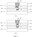
- FIG. 5 is a schematic diagram of a structure of a semiconductor device according to an embodiment of this application.
- the second connection pad 430 and the first connection pad 330 may be disposed opposite to each other in a vertical direction.
- the vertical through hole 359 may expose the sidewalls of the second connection pad 430 and the first connection pad 330, and the exposed sidewalls of the second connection pad 430 and the first connection pad 330 are flush with each other.
- the contact plug 360 in the vertical through hole 359 is separately connected to the sidewall of the second connection pad 430 and the sidewall of the first connection pad 330, to electrically connect the second connection pad 430 and the first connection pad 330.
- the second connection pad 430 may be aligned with the first connection pad 330 on one side.
- the sidewall on one side of the first connection pad 330 exceeds the sidewall of the second connection pad 430 in the horizontal direction.
- the contact plug 360 may be in contact with the upper surface and the sidewall on one side of the first connection pad 330 and the sidewall on one side of the second connection pad 430. As shown in FIG.
- the second connection pad 430 may be aligned with the first connection pad 330 on a plurality of sides.
- the contact plug 360 may be in contact with the upper surface and the sidewall on a plurality of sides of the first connection pad 330 and the sidewall on a plurality of sides of the second connection pad 430.
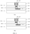
- FIG. 6 is a schematic diagram of a structure of another semiconductor device according to an embodiment of this application.
- the second connection pad 430 may be disposed opposite to the first connection pad 330 in the vertical direction.
- the sidewall on at least one side of the second connection pad 430 exceeds the sidewall of the first connection pad 330 in the horizontal direction.
- the formed vertical through hole 359 exposes at least a part of a surface on a side of the second connection pad 430 exceeding the first connection pad 330 in the horizontal direction, that is, exposes the upper surface adjacent to the sidewall of the second connection pad 430 exceeding the first connection pad 330 in the horizontal direction and exposes the sidewall and the upper surface adjacent to the sidewall of the second connection pad 430 exceeding the first connection pad 330 in the horizontal direction.
- the contact plug 360 filled in the vertical through hole 359 is at least in contact with the upper surface of the second connection pad 430.
- the vertical through hole 359 may further expose the upper surface of the first connection pad 330, so that the contact plug 360 can connect the first connection pad 330 and the second connection pad 430.
- the sidewall on one side of the second connection pad 430 may exceed the first connection pad 330 in the horizontal direction.
- the sidewall on one side of the second connection pad 430 may be aligned with the first connection pad 330, and the sidewall on another side of the second connection pad 430 exceeds the sidewall of the first connection pad 330 in the horizontal direction.
- the contact plug 360 may be in contact with the upper surface and the sidewall on a plurality of sides of the first connection pad 330, and the sidewall on one side and the upper surface on another side of the second connection pad 430. As shown in FIG.
- the sidewall on one side of the second connection pad 430 may exceed the first connection pad 330 in the horizontal direction, and the sidewall on another side wall of the second connection pad 430 is concave relative to the first connection pad 330.
- the contact plug 360 may be in contact with the upper surface and the sidewall on one side of the first connection pad 330, and the second connection pad 430 exceeds the upper surface on one side of the second connection pad 430 exceeding the first connection pad 330 in the horizontal direction, as shown in FIG. 6(b) .
- FIG. 7 is a schematic diagram of a structure of still another semiconductor device according to an embodiment of this application.
- the contact plug 360 may be in contact with the upper surface and the sidewall on one side of the first connection pad 330, and the second connection pad 430 exceeds the upper surface on one side of the first connection pad 330.
- the contact plug 360 may be in contact with the upper surface and the sidewall on a plurality of sides of the first connection pad 330 and the upper surface of the second connection pad 430.
- the contact plug 360 may be in contact with the upper surface and the sidewall on a plurality of sides of the first connection pad 330, and the upper surface and the sidewall on a plurality of sides of the second connection pad 430.
- a part of the first dielectric layer may be reserved between the contact plug 360 and the first connection pad 330, to provide protection for the first connection pad 330 in an etching process.
- the contact plug 360 may connect the first connection pad 330 and the second connection pad 430 from a plurality of sides of the first connection pad 330, to improve, to some extent, a contact area between the contact plug 360 and the second connection pad 430 and improve contact reliability between the contact plug 360 and the second connection pad 430.
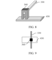
- FIG. 8 is a schematic diagram of a structure of a three-dimensional interconnection structure according to an embodiment of this application.
- FIG. 9 is a top view of a three-dimensional interconnection structure according to an embodiment of this application.
- the contact plug 360 forms an arch structure, to implement connection between the first connection pad 330 and the second connection pad 430.
- the contact plug 360 is formed on left and right sides of the first connection pad 330.
- a width between the left side and the right side of the first connection pad 330 may be relatively small.
- FIG. 10 is a schematic diagram of a structure of yet another semiconductor device according to an embodiment of this application.
- the second connection pad 430 and the first connection pad 330 are disposed in a staggered manner in the vertical direction. In other words, there is no overlapping region between the second connection pad 430 and the first connection pad 330 in a direction perpendicular to the bonding surface 1001. Therefore, a size of the top opening of the vertical through hole 359 is greater than or equal to the horizontal distance between the second connection pad 430 and the first connection pad 330.
- the vertical through hole 359 may expose the opposite sidewalls of the first connection pad 330 and the second connection pad 430, that is, expose the sidewall of the first connection pad 330 facing the second connection pad 430, and expose the sidewall of the second connection pad 430 facing the first connection pad 330.
- the vertical through hole 359 has even a horizontal size at different depths, so that the metal plug 360 in the vertical through hole 359 can connect the exposed sidewalls of the first connection pad 330 and the second connection pad 430, to implement electrical connection between the first connection pad 330 and the second connection pad 430.
- the size of the top opening of the vertical through hole 359 may be greater than the lateral sizes of the second connection pad 430 and the first connection pad 330.
- the vertical through hole 359 may further expose a part of the upper surface of the first connection pad 330 and/or a part of the upper surface of the second connection pad 430.
- a part of the first dielectric layer may be reserved for the sidewall of the first connection pad 330, to provide protection for the first connection pad 330, as shown in FIG. 10(b) .
- FIG. 11 is a schematic diagram of other shapes of a first connection pad and a second connection pad according to an embodiment of this application.
- a shape of the first connection pad 330 may be a slit shape or a comb tooth shape.
- a shape of the second connection pad 430 may be a polygon, a circle, a slit shape, or a comb tooth shape.
- the shape of the first connection pad 330 is a polygon or a circle
- the shape of the second connection pad 430 may be a slit shape or a comb tooth shape.
- the slit shape may be a single slit shape or a multi-slit shape.
- the slit shape may include a single slit shape with reference to FIG.
- a quantity of comb teeth in the comb tooth shape may be determined according to an actual case.
- the slit shape or the comb tooth shape may be considered as a combination of a plurality of lines.
- the formed vertical through hole 359 may expose or may not expose a sidewall of a connection pad with the slit shape or the comb tooth shape, provided that the vertical through hole 359 can expose both a part of the upper surface of the first connection pad 330 and a part of the upper surface of the second connection pad 430, to implement contact between the contact plug 360 and each of the first connection pad 330 and the second connection pad 430.
- FIG. 12 is a schematic diagram of a structure of still yet another semiconductor device according to an embodiment of this application.
- the second connection pad 430 is in the single slit shape.
- the contact plug 360 may be connected to the upper surface and the sidewall of the first connection pad 330 and the upper surface of the second connection pad 430.
- the contact plug 360 may be connected to the upper surface and the sidewall of the first connection pad 330 and the upper surface and the sidewall of the second connection pad 430.
- the second connection pad 430 is in a double slit shape.
- the contact plug 360 may be connected to the upper surface and the sidewall of the first connection pad 330 and the sidewall of the second connection pad 430.
- the vertical through hole 359 may be a through hole passing through the upper surface of the first wafer 300 to the upper surface of the first connection pad 330, and passing through the periphery of the first connection pad 330 to the upper surface of the second connection pad 430.
- the through hole exposes the upper surface of the first connection pad 330 and the upper surface and/or the sidewall of the second connection pad 430, to form the vertical through hole 359 with a relatively large size at an upper part and a relatively small size at a lower part.
- FIG. 13 is a schematic diagram of a structure of a further semiconductor device according to an embodiment of this application. Specifically, as shown in FIG. 3 , a size of the vertical through hole 359 in the first substrate 310 may be different from a size of the vertical through hole in the first dielectric layer 320. As shown in FIG. 13(a) and FIG. 13(c) , a size of the vertical through hole 359 above the upper surface of the first connection pad 330 may be different from a size of the vertical through hole 359 below the upper surface of the first connection pad 330. As shown in FIG.
- a size of the vertical through hole 359 above the lower surface of the first connection pad 330 may be different from a size of the vertical through hole 359 below the lower surface of the first connection pad 330.
- a size of the vertical through hole 359 above the upper surface of the second connection pad 430 may be different from a size of the vertical through hole 359 below the upper surface of the second connection pad 430.
- the semiconductor device provided in this embodiment of this application may further include a third wafer.
- FIG. 14 is a schematic diagram of a structure of still further semiconductor device according to an embodiment of this application.
- the first wafer 300, the second wafer 400, and the third wafer 500 form three stacked layers.
- the third wafer 500 may include a third substrate 510.
- a third dielectric layer 520 may be formed on the third substrate 510.
- the third dielectric layer 520 may have a third connection pad 530.
- the third wafer 500 may be disposed on the first wafer 300. Electrical connection is implemented between the third connection pad 530 in the third wafer 500 and the contact plug 360 through bonding between the first wafer 300 and the third wafer 500.
- the third connection pad 530 and the contact plug 360 may be connected (not shown in the figure) by using another contact plug formed by using a manufacturing process similar to the contact plug 360, after the dielectric layers of the first wafer 300 and the third wafer 500 are bonded.
- a bonding surface 5001 between the first wafer 300 and the third wafer 500 refer to FIG. 14 .
- the embodiments of this application provide the semiconductor device.
- the semiconductor device includes the first wafer, the second wafer, and the contact plug.
- the first wafer may include the first dielectric layer.
- the first dielectric layer has the first connection pad.
- the second wafer is bonded to the first wafer.
- the second wafer includes the second dielectric layer.
- the second dielectric layer has the second connection pad.
- the contact plug is a conductive material filled in the vertical through hole.
- the contact plug is configured to electrically connect the first connection pad and the second connection pad.
- the vertical through hole is a through hole that is formed through etching and that passes through the first wafer and partially passes through the second wafer to the upper surface and/or the sidewall of the second connection pad.
- the first connection pad is located in the vertical through hole.
- connection plug in the vertical through hole may be in contact with the upper layer of the first connection pad and the upper layer and/or the sidewall of the second connection pad, to implement electrical connection between the first connection pad and the second connection pad and implement vertical interconnection between the first wafer and the second wafer.
- the connection plug serves as a signal transmission path between the first connection pad and the second connection pad. This path is relatively short. Therefore, a signal delay is reduced.
- the vertical through hole is formed by using an etching process, and passes through the sidewall of the first connection pad to the second connection pad.
- the contact plug may be in contact with the second connection pad from the periphery of the first connection pad, to implement reliable connection between the contact plug and the second connection pad by using a simple process.
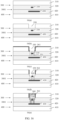
- FIG. 15 is a flowchart of a manufacturing method of a semiconductor device according to an embodiment of this application.
- FIG. 16 to FIG. 20 are schematic diagrams of a semiconductor device in a manufacturing process of the semiconductor device according to an embodiment of this application. The method may include the following steps:
- S101 Provide a first wafer 300 and a second wafer 400 between which bonding is completed, with reference to FIG. 16(a) , FIG. 17(a) , FIG. 18(a) , FIG. 19(a) , and FIG. 20(a) .
- the first wafer 300 may include a first substrate 310, a first dielectric layer 320 on the first substrate 310, and a first connection pad 330 in the first dielectric layer 320.
- the second wafer 400 may include a second substrate 410, a second dielectric layer 420 on the second substrate 410, and a second connection pad 430 in the second dielectric layer 420.
- the same device structure or different device structures may be formed on the first substrate 310 and the second substrate 410.
- devices on the first substrate 310 and the second substrate 410 may be both DRAM devices, or both logic devices, or respectively two devices of a DRAM device and a logic device, or separately two devices in a SRAM device and a logic device, or separately two devices in a CIS and an ISP.
- the first connection pad 330 is a connection pad in the interconnection structure of the first wafer 300 before the bonding, and may be a top metal layer (top metal) in the first wafer 300.
- a material of the first connection pad 330 may be metal copper.
- the first connection pad 330 may be covered by the first dielectric layer 320, to implement isolation between different first connection pads 330.
- the first dielectric layer 320 may be a silicon oxide layer, or may be a stacked structure, for example, may include a silicon nitride layer and a silicon oxide layer on the silicon nitride layer.
- the second connection pad 430 is a connection pad in the interconnection structure of second first wafer 400 before the bonding, and may be a top metal layer in the second wafer 400.
- a material of the second connection pad 430 may be metal copper.
- the second connection pad 430 may be covered by the second dielectric layer 420, to implement isolation between different second connection pads 430.
- the second dielectric layer 420 may be a silicon oxide layer, or may be a stacked structure, for example, may include a silicon nitride layer and a silicon oxide layer on the silicon nitride layer.
- a surface on which a device structure is formed on the first substrate 310 is used as a front surface of the first wafer 300, and a surface opposite to the surface on which a device is formed on the first substrate 310 is used as a back surface of the first wafer 300; and a surface on which a device structure is formed on the second substrate 410 is used as a front surface of the second wafer 400, and a surface opposite to the surface on which a device is formed on the second substrate 410 is used as a back surface of the second wafer 400.
- the first wafer 300 may be bonded to the second wafer 400.
- the first wafer 300 and the second wafer 400 may be two wafers in a plurality of bonded wafers.
- the front surface of the first wafer 300 may be bonded to the front surface of the second wafer 400.
- the front surface of the first wafer 300 may alternatively be bonded to the back surface of the second wafer 400.
- the back surface of the first wafer 300 may alternatively be bonded to the front surface of the second wafer 400.
- the back surface of the first wafer 300 may alternatively be bonded to the back surface of the second wafer 400.
- a material layer used for bonding may be formed on a surface used for bonding the first wafer 300 and the second wafer 400 is a bonding surface.
- the bonding material layer may be an adhesive layer with a dielectric material, for example, silicon oxide or silicon nitride, to implement bonding between the two wafers by using molecular forces at the adhesive layer.
- the two wafers are bonded by using dielectric layers, and vertical interconnection is not implemented between the first connection pad 330 in the first wafer 300 and the second connection pad 430 in the second wafer 400. Therefore, connection between the first wafer 300 and the second wafer 400 needs to be implemented.
- S102 Use the first connection pad as a blocking layer, etch the first wafer 300 from top to bottom to form a vertical through hole 359.
- the vertical through hole 359 passes through the first wafer to an upper surface of the first connection pad 330, passes through the first wafer and the second wafer to the second connection pad 430 along the sidewall of the first connection pad 330, and exposes an upper surface and/or a sidewall of the second connection pad 430.
- the first wafer 300 may be used as an upper wafer in the bonding structure. Etching is performed on the upper surface of the first wafer 300, to form the vertical through hole 359. It may be understood that, when the back surface of the first wafer 300 is used as a bonding surface 1001, etching may be performed on the front surface of the first wafer 300; or when the front surface of the first wafer 300 is used as a bonding surface 1001, etching may be performed on the back surface of the first wafer 300.
- the vertical through hole 359 may expose the entire upper surface of the first connection pad 330, or may expose a part of the upper surface of the first connection pad 330.
- the vertical through hole 359 may expose the sidewall on one or more sides of the first connection pad 330, or may not expose the sidewall of the first connection pad 330. In this case, the sidewall of the first connection pad 330 is covered by a part of the first dielectric layer, to provide protection for the first connection pad 330.
- the vertical through hole 359 may expose the entire upper surface of the second connection pad 430, or may expose a part of the upper surface of the second connection pad 430.
- the vertical through hole 359 may expose the sidewall on one or more sides of the second connection pad 430, or may not expose the sidewall of the second connection pad 430. In this case, the sidewall of the second connection pad 430 is covered by the second dielectric layer.
- the following uses bonding between the front surface of the first wafer 300 and the second wafer 400 as an example for description.
- the second connection pad 430 is disposed opposite to the first connection pad 330 in a vertical direction.
- the second connection pad 430 is located below the first connection pad 330.
- the sidewall of the second connection pad 430 may be flush with the sidewall of the first connection pad 330, or the sidewall of the second connection pad 430 exceeds the sidewall of the first connection pad 330 in the horizontal direction.
- a manner of forming the vertical through hole 359 may be specifically as follows: first etching the upper surface of the first wafer to obtain a first opening, where the first opening is located above the first connection pad 330, and a sidewall on at least one side of the first opening may exceed the sidewall of the first connection pad 330 in the horizontal direction.
- the first opening is deepened, to expose the first connection pad 330.
- Etching is performed in a position in which a bottom of the first opening exceeds the sidewall of the first connection pad 330 in the horizontal direction.
- a second opening to the second connection pad 430 may be formed around the periphery of the first connection pad 330, to form the vertical through hole 359.
- the first connection pad 330 may protect the first dielectric layer and the second dielectric layer under the first connection pad 330.
- a position of the second opening may be determined based on a position of the second connection pad 430 relative to the first connection pad 330.
- a direction in which the sidewall of the second connection pad 430 exceeds the sidewall of the first connection pad 330 in the horizontal direction may be consistent with a direction in which the sidewall of the second opening exceeds the sidewall of the first connection pad 330.
- the sidewall on a plurality of sides of the second connection pad 430 exceeds the sidewall of the first connection pad 330 in the horizontal direction.
- etching may be performed on the back surface of the first wafer 300, that is, etching is performed on the back surface of the first substrate 310 to form the first opening 350.
- the first opening 350 may be above the first connection pad 330, and the sidewall on a plurality of sides of the first opening 350 extends the sidewall of the first connection pad 330 in the horizontal direction.
- Etching of the first opening 350 may be stopped in a position of the lower surface of the first substrate 310, or etching may be performed on a part of the first dielectric layer 320 (not shown in the figure) and stopped in the first dielectric layer 320.
- An insulating layer 361 is deposited to protect the sidewall of the first opening 350. As shown in FIG.
- etching is performed on the bottom in the position in which the sidewall of the first opening 350 exceeds the first connection pad 330 in the horizontal direction (in this time of etching, the sidewall of the first connection pad 330 may be exposed, or a part of the first dielectric layer 320 may be reserved and the sidewall of the first connection pad 330 may be not exposed), to form a second opening 351 to the bonding surface 1001.
- the first connection pad 330 is used as a blocking layer, and the first opening 350 and the second opening 351 are deepened together, to remove the first dielectric layer 320 above the first connection pad 330 and the second dielectric layer 420 above the second connection pad 430, thereby forming the vertical through hole 359. As shown in FIG.
- the formed vertical through hole 359 exposes the upper surface of the first connection pad 330, and a part of the upper surface on a plurality of sides of the second connection pad 430 exceeding the first connection pad 330 in the horizontal direction.
- a part of the first dielectric layer 320 on the sidewall of the first connection pad 330 is reserved, to protect the first connection pad 330 and avoid damage or collapse caused due to etching performed on the first connection pad 330.
- the second dielectric layer of the sidewall of the second connection pad 430 may be etched to expose the sidewall of the second connection pad 430.
- etching is performed from the back surface of the first wafer 300.
- etching is performed from the back surface of the first substrate 310 to form the first opening 350.
- etching of the first opening 350 may be stopped in a position of a lower surface of the first substrate 310, or etching may be performed on a part of the first dielectric layer 320 (not shown in the figure) and stopped in the first dielectric layer 320.
- an insulating layer 361 is deposited to protect the sidewall of the first opening 350.
- etching is performed at a bottom in a position in which the sidewall of the first opening 350 exceeds the first connection pad 330 in the horizontal direction to form a second opening 351 to the bonding surface 1001.
- the first connection pad 330 is used as a blocking layer, and the first opening 350 and the second opening 351 are deepened together, so that the deepened second opening 351 is stopped at the lower surface of the second connection pad 430.
- the first connection pad 330 may protect the first dielectric layer and the second dielectric layer below the first connection pad 330, to form a vertical through hole 359.
- the vertical through hole 359 exposes the upper surface of the first connection pad 330, and a part of the upper surface and the sidewall on a plurality of sides of the second connection pad 430 extending the first connection pad 330.
- the dielectric layers of the sidewalls of the first connection pad 330 and the second connection pad 430 may be removed through etching, to expose the sidewalls of the first connection pad 330 and the second connection pad 430.
- steps shown in FIG. 16 Details are not described herein again.
- the second connection pad 430 is disposed opposite to the first connection pad 330 in the vertical direction.
- the second connection pad 430 is located below the first connection pad 330.
- the sidewall of the second connection pad 430 may be flush with the sidewall of the first connection pad 330, or the sidewall of the second connection pad 430 may exceed the sidewall of the first connection pad 330 in the horizontal direction.
- a third opening may be formed in the first wafer before bonding between wafers.
- the third opening is formed in the first dielectric layer around the first connection pad 330. In this way, an etching load after the bonding may be reduced.
- a manner of forming the vertical through hole may be specifically as follows: After the bonding between wafers, etching is performed on the upper surface of the first wafer to form a first opening, where the first opening is located above the first connection pad 330, and the sidewall on at least one side of the first opening may exceed the sidewall of the first connection pad 330 in the horizontal direction. In this way, the first opening may deepened to expose the first connection pad 330. In addition, the first opening may be connected to the third opening, and the third opening may be deepened. The deepened third opening may expose the second connection pad 430, to form the vertical through hole 359.
- the first connection pad 330 may protect the first dielectric layer and the second dielectric layer under the first connection pad 330.
- a position of the third opening may be determined based on a position of the second connection pad 430 relative to the first connection pad 330.
- a direction in which the sidewall of the second connection pad 430 exceeds the sidewall of the first connection pad 330 in the horizontal direction may be consistent with a direction in which the third opening is disposed in the first dielectric layer.
- a third opening 352 may be formed in the first wafer 300.
- the third opening 352 is formed in the first dielectric layer 320 around the first connection pad 330.
- etching may be performed on the first dielectric layer 320, to form the third opening 352 around the first connection pad 330.
- etching may be performed on the back surface of the first wafer 300, that is, etching is performed on the back surface of the first substrate 310 to form the first opening 350.
- the first opening 350 may be above the first connection pad 330, and the sidewall on a plurality of sides of the first opening 350 extends the sidewall of the first connection pad 330 in the horizontal direction.
- etching of the first opening 350 may be stopped in a position of the lower surface of the first substrate 310, or etching may be performed on a part of the first dielectric layer 320 (not shown in the figure) and stopped in the first dielectric layer 320. As shown in FIG.
- an insulating layer 361 is deposited to protect the sidewall of the first opening 350.
- the first connection pad 330 serves as a blocking layer.
- the first opening 350 is deepened to connect the first opening 350 to the third opening. Then, etching is further performed to deepen the third opening 352. Therefore, the deepened first opening 350 exposes the upper surface of the first connection pad, and the deepened third opening 352 exposes the upper surface of the second connection pad 430 to form the vertical through hole 359, as shown in FIG. 18(d) .
- the second dielectric layer of the sidewall of the second connection pad 430 may be etched to expose the sidewall of the second connection pad 430. Examples are not provided for description herein. In a direction in which the second connection pad 430 is flush with the first connection pad 330, the dielectric layers of the sidewalls of the first connection pad 330 and the second connection pad 430 may be removed through etching, to expose the sidewalls of the first connection pad 330 and the second connection pad 430. For specific operation steps, refer to steps shown in FIG. 18 . Details are not described herein again.
- the second connection pad 430 is disposed opposite to the first connection pad 330 in a vertical direction.
- the second connection pad 430 is located below the first connection pad 330.
- the sidewall of the second connection pad 430 may be flush with the sidewall of the first connection pad 330, or the sidewall of the second connection pad 430 exceeds the sidewall of the first connection pad 330 in the horizontal direction.
- a manner of forming the vertical through hole 359 may be specifically as follows: first etching the upper surface of the first wafer to obtain a first opening, where the first opening is located above the first connection pad 330, and a sidewall on at least one side of the first opening may exceed the sidewall of the first connection pad 330 in the horizontal direction.
- the first opening may be deepened, to expose the first connection pad 330.
- the first opening is further deepened.
- the first connection pad 330 may protect the first dielectric layer and the second dielectric layer below the first connection pad 330.
- Etching is performed on the first dielectric layer and the second dielectric layer in a position in which the first opening exceeds the first connection pad 330 in the horizontal direction.
- the deepened first opening around the first connection pad 330 may pass through the second connection pad 430 around the first connection pad 330, to form the vertical through hole 359.
- the sidewall on a plurality of sides of the second connection pad 430 exceeds the sidewall of the first connection pad 330 in the horizontal direction.
- Etching is performed on the back surface of the first wafer 300, that is, etching is performed on the back surface of the first substrate 310, to form the first opening 350.
- the first opening 350 may be above the first connection pad 330, and the sidewall on a plurality of sides of the first opening 350 exceeds the sidewall of the first connection pad 330.
- etching of the first opening 350 may be stopped in a position of the lower surface of the first substrate 310, or etching may be performed on a part of the first dielectric layer 320 (not shown in the figure) and stopped in the first dielectric layer 320.
- the insulating layer 361 is deposited to protect the sidewall of the first opening 350.
- the first opening 350 is deepened.
- the second connection pad 430 is used as an etching stop layer.
- the first connection pad 330 provides protection for the first dielectric layer and the second dielectric layer under the first connection pad 330 until the upper surface of the second connection pad 430 is exposed.
- the upper surface of the first connection pad 330 is also exposed in the deepened first opening 350 to form the vertical through hole 359.
- the second connection pad 430 is disposed opposite to the first connection pad 330 in a vertical direction.
- the second connection pad 430 is located below the first connection pad 330.
- the sidewall of the second connection pad 430 may be flush with the sidewall of the first connection pad 330, or the sidewall of the second connection pad 430 exceeds the sidewall of the first connection pad 330 in the horizontal direction.
- a manner of forming the vertical through hole 359 may be specifically as follows: etching the upper surface of the first wafer to form a fourth opening. A sidewall on at least one side of the fourth opening exceeds the sidewall of the first connection pad 330. Then, the first connection pad 330 may be used as a blocking layer.
- Etching is performed on an upper part of the first connection pad 330 and a bottom part of the fourth opening, to expose the upper surface of the first connection pad 330.
- the deepened fourth opening exposes the upper surface and/or the sidewall of the second connection pad 430.
- the first connection pad 330 may protect the first dielectric layer and the second dielectric layer below the first connection pad 330.
- the sidewall on a plurality of sides of the second connection pad 430 exceeds the sidewall of the first connection pad 330.
- Etching is performed on the back surface of the first wafer 300, that is, etching is performed on the back surface of the first substrate 310.
- An etching position is around the first connection pad 330.
- etching is stopped in a position of the lower surface or the upper surface of the first connection pad 330, to obtain the fourth opening 353.
- the insulating layer 361 is deposited to protect the sidewall of the fourth opening 353.
- Etching is performed on the first dielectric layer 320 on the upper part of the first connection pad 330 and the first dielectric layer 320 and the second dielectric layer 420 at the bottom of the fourth opening 353 around the first connection pad 330, to expose the upper surface and the sidewall of the first connection pad 330 and the upper surface of the second connection pad 430, thereby forming the vertical through hole 359, as shown in FIG. 20(d) .
- the first connection pad 330 of the upper-layer wafer is used as a blocking layer; and etching is stopped when the second connection layer 430 of the lower-layer wafer is exposed.
- the first connection pad 330 is a conductive material.
- a material with relatively large etch selectivity may be set for the first dielectric layer and the second dielectric layer, for example, a metal material or a doped semiconductor material. Etching selectivity between metal and a dielectric layer is relatively large, for example, SiO 2 :Al is close to 20:1, and SiO 2 :W is close to 80:1.
- the first connection pad 330 and the second connection layer 430 are not greatly damaged, to ensure that the first connection pad 330 still exists before etching is performed on the second connection layer 430 until etching is performed on both the first dielectric layer 320 and the second dielectric layer 420. Etching is stopped at the second connection layer 430 of the lower wafer.
- the etching process is relatively simple.
- S103 Fill the vertical through hole 359 with a conductive material to form a contact plug 360, with reference to FIG. 16(e) , FIG. 17(e) , FIG. 18(e) , FIG. 19(e) , and FIG. 20(e) .
- etching may be started from the upper surface of the first wafer 300, to form the vertical through hole 359 as the vertical through hole 359.
- the upper surface of the first connection pad 330 and the upper surface and/or the sidewall of the second connection pad 430 are exposed.
- the formed contact plug 360 is in contact with the upper surface of the first connection pad 330, and also in contact with the upper surface and/or the sidewall of the second connection pad 430.
- the formed contact plug 360 is in contact with both the first connection pad 330 and the second connection pad 430, to implement electrical connection between the first connection pad 330 and the second connection pad 430.
- the contact plug 360 is formed in the vertical through hole 359.
- a conductive material may be formed in the vertical through hole 359 in an electroplating manner or a deposition manner. Then, the conductive material outside the vertical through hole 359 is removed by using a planarization process, for example, a chemical mechanical polishing process, to form the contact plug 360.
- a material of the contact plug 360 may be copper or aluminum, or may be another conductive metal material or a non-metal material, for example, may be doped silicon.
- the first wafer and the second wafer that are bonded are provided.
- the first wafer includes the first dielectric layer.
- the first dielectric layer has the first connection pad.
- the second wafer includes the second dielectric layer.
- the second dielectric layer has the second connection pad.
- the first connection pad is used as a blocking layer.
- Etching is performed on the first wafer from top to bottom to form the vertical through hole.
- Thee vertical through hole passes through the first wafer to the upper surface of the first connection pad, passes through the second wafer to the second connection pad along the sidewall of the first connection pad, and exposes the upper surface and/or the sidewall of the second connection pad.
- the conductive material is filled in the vertical through hole to form the contact plug.
- the vertical through hole may expose the upper surface of the first wafer and the upper surface and/or the sidewall of the second connection pad.
- the contact plug in the vertical through hole may be in contact with both the first connection pad and the second connection pad, to implement electrical connection between the first connection pad and the second connection pad.
- the contact plug serves as a signal transmission path between the first connection pad and the second connection pad. This path is relatively short. Therefore, a signal delay is reduced.
- the vertical through hole is formed by using an etching process, and passes through the sidewall of the first connection pad to the second connection pad.
- the contact plug may be in contact with the second connection pad from the periphery of the first connection pad, to implement reliable connection between the contact plug and the second connection pad by using a simple process.
- only one metal plug exists, and therefore, a distance between two metal plugs does not need to be considered. Therefore, a lateral size may be reduced to some extent, to reduce a device size and improve device integration.
Abstract
Description
- This application relates to the field of semiconductor manufacturing technologies, and in particular, to a semiconductor structure and a manufacturing method thereof.
- In recent years, a semiconductor device and an integrated circuit have rapidly increasing integration density and power density. In this case, plane space is limited, and a Moore's law goes to a bottleneck. A three-dimensional stacking technology is a current mainstream breakthrough solution. A multi-layer or 3D structure may be formed by using the three-dimensional stacking technology. The 3D structure is, for example, a three-dimensional integrated circuit (three dimensional integrated circuit, 3D-IC), a micro-electro-mechanical system (Micro-Electro-Mechanical System, MEMS), or a complementary metal oxide semiconductor (complementary metal oxide semiconductor, CMOS) image sensor (CMOS image sensor, CIS). In the three-dimensional stacking technology, bonding is a core process that experiences a technology iteration process from a micro-bump (micro-bump) bonding technology, to a Cu pillar (Cu pillar) bonding technology, and to a wafer bonding technology. Currently, the three-dimensional stacking technology centers on the wafer bonding technology. The wafer bonding technology has been developed into a competition key of each manufacturer in the three-dimensional stacking technology.
- The wafer bonding is a technology for fitting wafers and wafer surfaces to form a mechanical connection and an electrical connection. Dielectric layer bonding is a wafer bonding implementation of a wafer bonding technology for forming a covalent bond between dielectric layers. In this case, electric connection is not implemented between two wafers that are bonded. To implement interconnection between wafers bonded through dielectric layers, a through silicon via (Through Silicon Via, TSV) technology may be used. In the TSV technology, a through hole is formed on a back surface of a wafer, and a conductive material is filled in the through hole, to implement vertical interconnection between wafers. For example, two through holes are separately disposed on different wafers, and the conductive material is filled in the through holes, to obtain a contact plug separately connected to the two wafers. Then, a connection line separately connected to the two wafers is further disposed, to implement connection between different wafers. In this manner, the contact plug and the connection line are used between the two wafers to implement connection. A cable between the two wafers is relatively long, causing a relatively signal delay. In this case, an actual requirement cannot be met in some scenarios. In addition, three-dimensional interconnection is implemented by using a plurality of contact plugs, occupying relatively large plane space. This does not facilitate improvement of integrity density of a device.
- In view of this, a first aspect of this application provides a semiconductor structure and a manufacturing method thereof, to reduce a signal delay between wafers.
- According to a first aspect, an embodiment of this application provides a semiconductor device. The semiconductor device may include a first wafer, a second wafer, and a contact plug. The first wafer may include a first dielectric layer. The first dielectric layer may have a first connection pad. The first connection pad may be configured to lead out a signal of the first wafer. The second wafer is bonded to the first wafer. The second wafer may include a second dielectric layer. The second dielectric layer may have a second connection pad. The second connection pad may be configured to lead out a signal of the second wafer. The contact plug may be a conductive material filled in a vertical through hole. The contact plug is configured to electrically connect the first connection pad and the second connection pad. The vertical through hole is a through hole that is formed through etching and that passes through the first wafer and partially passes through the second wafer to an upper surface and/or a sidewall of the second connection pad. The first connection pad is located in the vertical through hole. The first dielectric layer located under the first connection pad is not etched. In this way, the contact plug in the vertical through hole may be in contact with an upper layer of the first connection pad and the upper layer and/or the sidewall of the second connection pad, to implement electrical connection between the first connection pad and the second connection pad and implement vertical interconnection between the first wafer and the second wafer. The contact plug serves as a signal transmission path between the first connection pad and the second connection pad. This path is relatively short. Therefore, a signal delay is reduced. In addition, the vertical through hole is formed by using an etching process, and passes through a sidewall of the first connection pad to the second connection pad. The contact plug may be in contact with the second connection pad from the periphery of the first connection pad, to implement reliable connection between the contact plug and the second connection pad by using a simple process. In addition, in this embodiment of this application, only one metal plug exists, and therefore, a distance between two metal plugs does not need to be considered. Therefore, a horizontal size may be reduced to some extent, to reduce a device size and improve device integration.
- In a possible implementation, the second connection pad is disposed opposite to the first connection pad in a vertical direction, and the sidewall on at least one side of the second connection pad exceeds the sidewall of the first connection pad in a horizontal direction. In this case, the vertical through hole exposes the upper surface adjacent to the sidewall on the at least one side of the second connection pad or the adjacent upper surface adjacent and the sidewall on the at least one side of the second connection pad.
- In this embodiment of this application, the sidewall on the at least one side of the second connection pad extends the sidewall of the first connection pad in the horizontal direction. In this case, the vertical through hole may expose at least the upper surface that is of the second connection pad and that is adjacent to the sidewall exceeding the first connection pad, to implement contact between the contact plug and the second connection pad. Certainly, the vertical through hole may further expose the sidewall of the second connection pad exceeding the first connection pad, to improve contact reliability between the contact plug and the second connection pad to some extent, thereby improving reliability of the electrical connection between the first connection pad and the second connection pad.
- In a possible implementation, the vertical through hole exposes the sidewall of the first connection pad; or in the vertical through hole, the first dielectric layer is reserved on the sidewall of the first connection pad.
- In this embodiment of this application, the vertical through hole may expose the sidewall of the first connection pad, to improve contact reliability between the contact plug formed in the vertical through hole and the first connection pad. Certainly, the vertical through hole may not expose the sidewall of the first connection pad. Instead, the first dielectric layer of the sidewall of the first connection pad is reserved in an etching process. In this way, the first dielectric layer may protect the sidewall of the first connection pad, to improve structure integrity of the first connection plate and further improve function integrity of the first connection pad.
- In a possible implementation, the second connection pad is disposed opposite to the first connection pad in a vertical direction, and the sidewall on at least one side of the second connection pad is flush with the sidewall of the first connection pad. In this case, the vertical through hole exposes the sidewall on the at least one side of the second connection pad and the sidewall of the first connection pad flush with the second connection pad.
- In this embodiment of this application, the sidewall on the at least one side of the second connection pad is flush with the sidewall of the first connection pad. In this case, the sidewall of the first connection pad and the sidewall of the second connection pad may be exposed by using the vertical through hole, so that the sidewall of the first connection pad is connected to the sidewall of the second connection pad by using the contact plug, to implement the electrical connection between the first connection pad and the second connection pad. Therefore, a redundant horizontal area of a vertical interconnection structure is reduced, to reduce a device area and improve device integration.
- In a possible implementation, the second connection pad and the first connection pad are disposed in a staggered manner in the vertical direction. A size of a top opening of the vertical through hole is greater than or equal to a horizontal distance between the second connection pad and the first connection pad.
- In this embodiment of this application, the second connection pad and the first connection pad may be disposed in the staggered manner in the vertical direction. In this case, there is no overlapping region between the first connection pad and the second connection pad in the vertical direction, and there is the horizontal distance between the first connection pad and the second connection pad in the horizontal direction. In this case, a size of a vertical through hole at a top opening may be greater than or equal to the horizontal distance between the second connection pad and the first connection pad, to successfully expose the first connection pad and the second connection pad, thereby implementing the electrical connection between the first connection pad and the second connection pad and improving reliability of the electrical connection.
- In a possible implementation, the semiconductor device further includes a third wafer.
- The third wafer has a third connection pad. The third wafer is bonded to the first wafer, to implement electrical connection between the third connection pad and the contact plug.
- In this embodiment of this application, the semiconductor device may further include the third wafer. The third connection pad of the third wafer may be electrically connected to the contact plug, and further connected to the first wafer and the second wafer. Specifically, the third wafer may be bonded to the first wafer, to further improve device integration.
- In a possible implementation, the vertical through hole passes through a multi-side sidewall direction of the first connection pad.
- In this embodiment of this application, the vertical through hole may pass through the multi-side sidewall of the first connection pad. In this way, the contact plug formed in the vertical through hole may enclose the first connection pad on a plurality of sides, to improve contact reliability between the contact plug and the first connection pad, increase a contact area between the contact plug and the second connection pad to some extent, and improve contact reliability between the contact plug and the second connection pad.
- According to a second aspect, an embodiment of this application provides a manufacturing method of a semiconductor device, including:
- providing a first wafer and a second wafer that are bonded, where the first wafer includes a first dielectric layer, the first dielectric layer has a first connection pad, the second wafer includes a second dielectric layer, and the second dielectric layer has a second connection pad;
- using the first connection pad as a blocking layer, and etching the first wafer from top to bottom to form a vertical through hole, where the vertical through hole passes through the first wafer to an upper surface of the first connection pad, passes through the second wafer to the second connection pad along the sidewall of the first connection pad, and exposes an upper surface and/or a sidewall of the second connection pad; and
- filling a conductive material in the vertical through hole to form a contact plug, where the contact plug is configured to implement electrical connection between the first connection pad and the second connection pad.
- In a possible implementation, the second connection pad is disposed opposite to the first connection pad in a vertical direction. The using the first connection pad as a blocking layer, and etching the first wafer from top to bottom to form a vertical through hole includes:
- etching the upper surface of the first wafer to obtain a first opening, where the first opening is located above the first connection pad, and a sidewall on at least one side of the first opening exceeds the sidewall of the first connection pad in a horizontal direction;
- forming a second opening through etching a bottom in a position at which the sidewall of the first opening exceeds the first connection pad in the horizontal direction; and
- using the first connection pad as the blocking layer, and deepening the first opening and the second opening, so that the deepened first opening exposes an upper surface of the first connection pad, and the deepened second opening exposes an upper surface and/or a sidewall of the second connection pad.
- In a possible implementation, in a direction in which the sidewall of the first opening exceeds the sidewall of the first connection pad in the horizontal direction, a sidewall on at least one side of the second connection pad extends the sidewall of the first connection pad in the horizontal direction. In this case, the deepened second opening exposes the upper surface adjacent to the sidewall of the second connection pad exceeding the first connection pad in the horizontal direction, or the sidewall of the second connection pad exceeding the first connection pad in the horizontal direction and the upper surface adjacent to the sidewall of the second connection pad.
- And/or, in a direction in which the sidewall of the first opening extends the sidewall of the first connection pad in the horizontal direction, a sidewall on at least one side of the second connection pad is flush with the sidewall of the first connection pad. In this case, the deepened second opening exposes the sidewall of the second connection pad flush with the first connection pad.
- In a possible implementation, in a direction in which the sidewall of the second connection pad exceeds the sidewall of the first connection pad in the horizontal direction, the first dielectric layer is reserved on the sidewall of the first connection pad in the deepened second opening.
- In a possible implementation, the second connection pad is disposed opposite to the first connection pad in a vertical direction. The first dielectric layer has a third opening. The using the first connection pad as a blocking layer, and etching the first wafer from top to bottom to form a vertical through hole includes:
- etching the upper surface of the first wafer to obtain a first opening, where the first opening is located above the first connection pad, and a sidewall on at least one side of the first opening exceeds the sidewall of the first connection pad in a horizontal direction; and
- using the first connection pad as the blocking layer, and etching the first dielectric layer and the second dielectric layer at a bottom of the first opening, so that the deepened first opening is connected to the third opening, the third opening is deepened in the etching process, the deepened first opening exposes an upper surface of the first connection pad, and the deepened third opening exposes an upper surface and/or a sidewall of the second connection pad.
- In a possible implementation, in a direction in which the sidewall of the first opening exceeds the sidewall of the first connection pad in the horizontal direction, a sidewall on at least one side of the second connection pad extends the sidewall of the first connection pad in the horizontal direction. The deepened third opening exposes the upper surface adjacent to the sidewall of the second connection pad exceeding the first connection pad in the horizontal direction, or the sidewall of the second connection pad exceeding the first connection pad in the horizontal direction and the upper surface adjacent to the sidewall of the second connection pad.
- And/or, in a direction in which the sidewall of the first opening extends the sidewall of the first connection pad in the horizontal direction, a sidewall on at least one side of the second connection pad is flush with the sidewall of the first connection pad. In this case, the deepened third opening exposes the sidewall of the second connection pad flush with the first connection pad.
- In a possible implementation, in a direction in which the sidewall of the second connection pad exceeds the sidewall of the first connection pad in the horizontal direction, the first dielectric layer is reserved on the sidewall of the first connection pad in the deepened third opening.
- In a possible implementation, the second connection pad is disposed opposite to the first connection pad in a vertical direction. The using the first connection pad as a blocking layer, and etching the first wafer from top to bottom includes:
- performing etching from the upper surface of the first wafer to obtain a first opening, where the first opening is located above the first connection pad, and a sidewall on at least one side of the first opening exceeds the sidewall of the first connection pad in a horizontal direction; and
- using the first connection pad as the blocking layer, and deepening the first opening, so that the deepened first opening exposes an upper surface of the first connection pad, and an upper surface and/or a sidewall of the second connection pad.
- In a possible implementation, in a direction in which the sidewall of the first opening exceeds the sidewall of the first connection pad in the horizontal direction, a sidewall on at least one side of the second connection pad extends the sidewall of the first connection pad in the horizontal direction. The deepened first opening exposes the upper surface adjacent to the sidewall of the second connection pad exceeding the first connection pad in the horizontal direction, or the sidewall of the second connection pad exceeding the first connection pad in the horizontal direction and the upper surface adjacent to the sidewall of the second connection pad.
- And/or, in a direction in which the sidewall of the first opening extends the sidewall of the first connection pad in the horizontal direction, a sidewall on at least one side of the second connection pad is flush with the sidewall of the first connection pad. In this case, the deepened first opening exposes the sidewall of the second connection pad flush with the first connection pad.
- In a possible implementation, the second connection pad is disposed opposite to the first connection pad in a vertical direction. The using the first connection pad as a blocking layer, and etching the first wafer from top to bottom includes:
- etching an upper surface of the first wafer to obtain a fourth opening, where a sidewall on at least one side of the fourth opening exceeds the sidewall of the first connection pad; and
- using the first connection pad as the blocking layer, and performing etching on the first connection pad and on a bottom of the fourth opening, to expose the upper surface of the first connection pad, where the deepened fourth opening exposes an upper surface and/or a sidewall of the second connection pad.
- In a possible implementation, in a direction in which the sidewall of the fourth opening exceeds the sidewall of the first connection pad in the horizontal direction, a sidewall on at least one side of the second connection pad extends the sidewall of the first connection pad in the horizontal direction. The deepened fourth opening exposes the upper surface adjacent to the sidewall of the second connection pad exceeding the first connection pad in the horizontal direction, or the sidewall of the second connection pad exceeding the first connection pad in the horizontal direction and the upper surface adjacent to the sidewall of the second connection pad.
- And/or, in a direction in which the sidewall of the fourth opening extends the sidewall of the first connection pad in the horizontal direction, a sidewall on at least one side of the second connection pad is flush with the sidewall of the first connection pad. In this case, the deepened fourth opening exposes the sidewall of the second connection pad flush with the first connection pad.
- In a possible implementation, the filling a conductive material in the vertical through hole to form a contact plug includes:
- forming a conductive material in the vertical through hole and on the upper surface of the first wafer by using an electroplating process or a deposition process; and
- removing the conductive material on the upper surface of the first wafer by using a planarization process, to form the contact plug in the vertical through hole.
- In comparison with the conventional technologies, this application has the following beneficial effects:
- It can be learned from the foregoing technical solutions that this application provides a semiconductor device and a manufacturing method thereof. The semiconductor device may include a first wafer, a second wafer, and a contact plug. The first wafer may include a first dielectric layer. The first dielectric layer has a first connection pad. The second wafer is bonded to the first wafer. The second wafer includes a second dielectric layer. The second dielectric layer has a second connection pad. The contact plug may be a conductive material filled in a vertical through hole. The contact plug is configured to electrically connect the first connection pad and the second connection pad. The vertical through hole is a through hole that is formed through etching and that passes through the first wafer and partially passes through the second wafer to an upper surface and/or a sidewall of the second connection pad. The first connection pad is located in the vertical through hole. The first dielectric layer located under the first connection pad is not etched. In other words, the vertical through hole may expose the upper surface of the first wafer and the upper surface and/or the sidewall of the second connection pad. In this way, the contact plug in the vertical through hole may be in contact with both the first connection pad and the second connection pad, to implement electrical connection between the first connection pad and the second connection pad. The contact plug serves as a signal transmission path between the first connection pad and the second connection pad. This path is relatively short. Therefore, a signal delay is reduced. In addition, the vertical through hole is formed by using an etching process, and passes through a sidewall of the first connection pad to the second connection pad. The contact plug may be in contact with the second connection pad from the periphery of the first connection pad, to implement reliable connection between the contact plug and the second connection pad by using a simple process. In addition, in this embodiment of this application, only one metal plug exists, and therefore, a distance between two metal plugs does not need to be considered. Therefore, a lateral size may be reduced to some extent, to reduce a device size and improve device integration.
- To clearly understand specific implementations of this application, the following briefly describes accompanying drawings used for describing the specific implementations of this application. Apparently, the accompanying drawings show merely some embodiments of this application.
-
FIG. 1 is a schematic diagram of a bonding structure in the conventional technologies; -
FIG. 2 is a top view of a three-dimensional interconnection structure in the conventional technologies; -
FIG. 3 is a schematic diagram of a structure of a semiconductor device according to an embodiment of this application; -
FIG. 4 is a schematic diagram of shapes of a first connection pad and a second connection pad according to an embodiment of this application; -
FIG. 5 is a schematic diagram of a structure of a semiconductor device according to an embodiment of this application; -
FIG. 6 is a schematic diagram of a structure of another semiconductor device according to an embodiment of this application; -
FIG. 7 is a schematic diagram of a structure of still another semiconductor device according to an embodiment of this application; -
FIG. 8 is a schematic diagram of a structure of a three-dimensional interconnection structure according to an embodiment of this application; -
FIG. 9 is a top view of a three-dimensional interconnection structure according to an embodiment of this application; -
FIG. 10 is a schematic diagram of a structure of yet another semiconductor device according to an embodiment of this application; -
FIG. 11 is a schematic diagram of other shapes of a first connection pad and a second connection pad according to an embodiment of this application; -
FIG. 12 is a schematic diagram of a structure of still yet another semiconductor device according to an embodiment of this application; -
FIG. 13 is a schematic diagram of a structure of a further semiconductor device according to an embodiment of this application; -
FIG. 14 is a schematic diagram of a structure of still further semiconductor device according to an embodiment of this application; -
FIG. 15 is a flowchart of a manufacturing method of a semiconductor device according to an embodiment of this application; and -
FIG. 16 to FIG. 20 are schematic diagrams of a semiconductor device in a manufacturing process of the semiconductor device according to an embodiment of this application. - To make the foregoing objectives, features, and advantages of this application clearer and more comprehensible, the following describes specific implementations of this application in more detail with reference to accompanying drawings.
- In the following descriptions, many specific details are described to facilitate full understanding of this application. However, this application may also be implemented in another manner different from that described herein, and a person skilled in the art may make similar promotion without violating a connotation of this application. Therefore, this application is not limited to the specific embodiments disclosed below.
- In addition, this application is described in detail with reference to schematic diagrams. When the embodiments of this application are described in detail, for ease of description, a cross section diagram indicating a device structure is not partially enlarged according to a general scale. The schematic diagram is merely an example, and shall not limit the protection scope of this application. In addition, three-dimensional spatial dimensions of length, width, and depth need to be considered in the actual manufacturing.
- In view of this, this application provides a semiconductor device and a manufacturing method thereof, to reduce a signal delay and an occupied area, thereby improving integration density of a device.
- As described in the background, different wafers can be bonded by using a three-dimensional stacking technology, to reduce plane space of a three-dimensional device and improve the integration density.
- For example,
FIG. 1 is a schematic diagram of a bonding structure in the conventional technologies. Afirst device 130 may be formed in afirst wafer 100. Thefirst device 130 may be, for example, a CIS. Asecond device 230 may be formed in asecond wafer 200. Thesecond device 230 may be, for example, an image system processor (image system processor, ISP). Then thefirst wafer 100 is bonded to thesecond wafer 200, to form an image sensor system. The first device is formed in adielectric layer 120 on asubstrate 110. The second device is formed in adielectric layer 220 on asubstrate 210. Abonding surface 1001 is formed between thefirst wafer 100 and thesecond wafer 200 that are bonded. - Specifically, dielectric layer bonding may be performed between the
first wafer 100 and thesecond wafer 200. Thesubstrate 110 of thefirst wafer 100 is etched by using a silicon via technology, to form a silicon via to the CIS and a silicon via to the ISP. After a metal material is filled in the two silicon vias, twometal plugs substrate 110 of thefirst wafer 100, to implement electrical connection between the twometal plugs redistribution layer 150 and each of the CIS and the ISP through the twometal plugs - However, in a manner of implementing connection through dielectric layer bonding and the silicon via technology, a signal of the ISP in the
second wafer 200 needs to be first transmitted upward through themetal plug 240 connected to the ISP, then transmitted to themetal plug 140 connected to the ISP through thehorizontal redistribution layer 150, and then transmitted downward to the CIS in thefirst wafer 100. With reference to a direction indicated by using a dashed line inFIG. 1 , the signal needs to pass through a relatively long π-shape path. A delay is related to resistance and capacitance in the path. Therefore, the signal transmission has a relatively large delay. In some scenarios, an actual requirement cannot be met. In addition, two metal plugs are needed to implement the connection between the CIS and the ISP.FIG. 2 is a top view of a three-dimensional interconnection structure in the conventional technologies. Minimum values of sizes of the twometal plugs metal plugs metal plugs first device 130 and thesecond device 140 in contact with the metal plugs 140 and 240 cannot be excessively small. Therefore, integration density of the device in this connection manner is affected. - Based on the foregoing technical problems, the embodiments of this application provide a semiconductor device and a manufacturing method thereof. The semiconductor device may include a first wafer, a second wafer, and a contact plug. The first wafer may include a first dielectric layer. The first dielectric layer has a first connection pad. The second wafer is bonded to the first wafer. The second wafer includes a second dielectric layer. The second dielectric layer has a second connection pad. The contact plug may be a conductive material filled in a vertical through hole. The contact plug is configured to electrically connect the first connection pad and the second connection pad. The vertical through hole is a through hole that is formed through etching and that passes through the first wafer and partially passes through the second wafer to an upper surface and/or a sidewall of the second connection pad. The first connection pad is located in the vertical through hole. The first dielectric layer located under the first connection pad is not etched. In other words, the vertical through hole may expose the upper surface of the first wafer and the upper surface and/or the sidewall of the second connection pad. In this way, the contact plug in the vertical through hole may be in contact with both the first connection pad and the second connection pad, to implement electrical connection between the first connection pad and the second connection pad. The contact plug serves as a signal transmission channel between the first connection pad and the second connection pad. This channel is relatively short. Therefore, a signal delay is reduced. In addition, the vertical through hole is formed by using an etching process, and passes through a sidewall of the first connection pad to the second connection pad. The contact plug may be in contact with the second connection pad from the periphery of the first connection pad, to implement reliable connection between the contact plug and the second connection pad by using a simple process. In addition, in this embodiment of this application, only one metal plug exists, and therefore, a distance between two metal plugs does not need to be considered. Therefore, a lateral size may be reduced to some extent, to reduce a device size and improve device integration.
- To more clearly understand specific implementations of this application, the following describes the semiconductor device provided in the embodiments of this application in detail with reference to the accompanying drawings.
-
FIG. 3 is a schematic diagram of a structure of a semiconductor device according to an embodiment of this application. The semiconductor device may include afirst wafer 300, asecond wafer 400, and acontact plug 360 for implementing vertical interconnection between thefirst wafer 300 and thesecond wafer 400. Thefirst wafer 300 may include afirst substrate 310, a firstdielectric layer 320 on thefirst substrate 310, and afirst connection pad 330 in thefirst dielectric layer 320. Thesecond wafer 400 may include asecond substrate 410, asecond dielectric layer 420 on thesecond substrate 410, and asecond connection pad 430 in thesecond dielectric layer 420. - The
first substrate 310 and thesecond substrate 410 may be semiconductor substrates, for example, Si substrates, Ge substrates, SiGe substrates, SOI (silicon on insulator, Silicon On Insulator), or GOI (germanium on insulator, Germanium On Insulator. In other embodiments, thefirst substrate 310 and thesecond substrate 410 may also be substrates including a semiconductor with another element or a semiconductor with another compound, for example, GaAs, InP, or SiC; or may be laminated structures, for example, Si/SiGe; or may be other epitaxial structures, for example, SGOI (germanium silicon on insulator). Thefirst substrate 310 and thesecond substrate 410 may be the same material, or may be different materials. In this embodiment, thefirst substrate 310 and thesecond substrate 410 may be silicon substrates. - All processes before bonding may be completed on the
first substrate 310 and thesecond substrate 410. For example, a device structure and an interconnection structure of electrically connected device structures are formed on thefirst substrate 310 and thesecond substrate 410. The device structure is covered by an inter-layer dielectric layer. The inter-layer dielectric layer may be silicon oxide. The interconnection structure is formed in a dielectric material. The device structure may be a MOS device, a storage device, and/or another passive device. The interconnection structure may be a multi-layer structure. The interconnection structure may include a contact plug, a via, or a connection layer. The connection layer may be located at a top layer of the interconnection structure. As a lead-out structure of the interconnection structure, the connection layer may include a plurality of connection pads. The interconnection structure may be a metal material, for example, tungsten, aluminum, or copper. In the diagram of this embodiment of this application, to merely simplify the accompanying drawing, only the connection layer at the top layer is shown. It may be understood that this is merely an example. In different designs and applications, an interconnection structure including a required quantity of layers may be formed according to a requirement. - The same device structure or different device structures may be formed on the
first substrate 310 and thesecond substrate 410. For example, devices on thefirst substrate 310 and thesecond substrate 410 may be both DRAM devices, or both logic devices, or separately two devices in a DRAM device and a logic device, or separately two devices in a SRAM device and a logic device, or separately two devices in a CIS and an ISP. - The same interconnection structure or different interconnection structures may be formed on the
first substrate 310 and thesecond substrate 410. Connection pads in the interconnection structures on thefirst substrate 310 and thesecond substrate 410 may have the same structure or different structures. For ease of differentiation, in this embodiment of this application, thefirst connection pad 330 in the interconnection structure on thefirst substrate 310 and thesecond connection pad 430 in the interconnection structure on thesecond substrate 410 are used as examples to describe interconnection structures between different wafers. - The
first connection pad 330 is a connection pad in the interconnection structure of thefirst wafer 300 before the bonding, and may be a top metal layer (top metal) in thefirst wafer 300. A material of thefirst connection pad 330 may be metal copper. Thefirst connection pad 330 may be covered by thefirst dielectric layer 320, to implement isolation between differentfirst connection pads 330. Thefirst dielectric layer 320 may be a silicon oxide layer, or may be a stacked structure, for example, may include a silicon nitride layer and a silicon oxide layer on the silicon nitride layer. - Similarly, the
second connection pad 430 is a connection pad in the interconnection structure of secondfirst wafer 400 before the bonding, and may be a top metal layer in thesecond wafer 400. A material of thesecond connection pad 430 may be metal copper. Thesecond connection pad 430 may be covered by thesecond dielectric layer 420, to implement isolation between differentsecond connection pads 430. Thesecond dielectric layer 420 may be a silicon oxide layer, or may be a stacked structure, for example, may include a silicon nitride layer and a silicon oxide layer on the silicon nitride layer. - For ease of description, a surface on which a device structure is formed on the
first substrate 310 is used as a front surface of thefirst wafer 300, and a surface opposite to the surface on which a device is formed on thefirst substrate 310 is used as a back surface of thefirst wafer 300; and a surface on which a device structure is formed on thesecond substrate 410 is used as a front surface of thesecond wafer 400, and a surface opposite to the surface on which a device is formed on thesecond substrate 410 is used as a back surface of thesecond wafer 400. - In this embodiment of this application, the
first wafer 300 may be bonded to thesecond wafer 400. Actually, thefirst wafer 300 and thesecond wafer 400 may be two wafers in a plurality of bonded wafers. The front surface of thefirst wafer 300 may be bonded to the front surface of thesecond wafer 400. The front surface of thefirst wafer 300 may alternatively be bonded to the back surface of thesecond wafer 400. The back surface of thefirst wafer 300 may alternatively be bonded to the front surface of thesecond wafer 400. The back surface of thefirst wafer 300 may alternatively be bonded to the back surface of thesecond wafer 400. A surface used for bonding thefirst wafer 300 and thesecond wafer 400 is a bonding surface. A material layer used for bonding may be formed on the bonding surface. The bonding material layer may be an adhesive layer with a dielectric material, for example, silicon oxide or silicon nitride, to implement bonding between the two wafers by using molecular forces at the adhesive layer. - It should be noted that, in this embodiment of this application, "upper" and "lower" are relative to each other, and are related to a bonding manner of the
first wafer 300 and the second wafer. Specifically, thefirst wafer 300 may be used as an upper wafer, and thesecond wafer 400 may be used as a lower wafer. When the front surface of thefirst wafer 300 is used as a bonding surface, thefirst wafer 300 is reversed, and original "upper" is changed to "lower". When the back surface of thefirst wafer 300 is used as a bonding surface, thefirst wafer 300 is not reversed, and original "upper" is still "upper". Similarly, when the front surface of thesecond wafer 400 is used as a bonding surface, thesecond wafer 400 is not reversed, and original "upper" is still "upper". When the back surface of thesecond wafer 400 is used as a bonding surface, the second wafer is reversed, and original "upper" is changed to "lower". In addition, descriptions such as upper, lower, left, right, front, back, top, and bottom are merely intended to facilitate indication of a relative position and/or a relative direction between devices, and are not intended to imply any specific fixed direction. - After the
first wafer 300 is bonded to thesecond wafer 400, the two wafers are bonded by using dielectric layers, and electric connection is not implemented between thefirst connection pad 330 in thefirst wafer 300 and thesecond connection pad 430 in thesecond wafer 400. Therefore, connection between thefirst wafer 300 and thesecond wafer 400 needs to be implemented by using a vertical throughhole 359. In this embodiment of this application, thefirst wafer 300 may be used as an upper wafer in the bonding structure. Etching is performed on the upper surface of thefirst wafer 300, to form the vertical throughhole 359. It may be understood that, when the back surface of thefirst wafer 300 is used as abonding surface 1001, etching may be performed on the front surface of thefirst wafer 300; or when the front surface of thefirst wafer 300 is used as abonding surface 1001, etching may be performed on the back surface of thefirst wafer 300. - Currently, etching may be performed on the upper surface of the first wafer by using a TSV technology, to form two through silicon vias passing through the first connection pad and the second connection pad. Then, a metal material is filled in the through silicon vias to form contact plugs. Afterwards, redistribution is performed on the upper surface of the first wafer, to establish connection between the two contact plugs. However, in this connection manner, a path between the first connection pad and the second connection pad is relatively long, a size of each contact plug is limited by an etching process and cannot be reduced without limitation, and a distance between the contact plugs is also limited. Therefore, a plane area occupied by two three-dimensional interconnected structures in this process is relatively large. In addition, because the contact plug is in contact with the first connection pad or the second connection pad, sizes of the first connection pad and the second connection pad are also limited by the etching process, and match sizes of the contact plugs. Therefore, the size of the first connection pad and the size of the second connection pad are relatively large. In addition, the distance between the first connection pad and the second connection pad corresponds to a horizontal distance between the contact plugs. The minimum distance between the first connection pad and the second connection pad is also limited. Therefore, a distribution design is also limited.
- To resolve the foregoing problem, in this embodiment of this application, etching may be started from the upper surface of the
first wafer 300. Thefirst connection pad 330 is used as a blocking layer to form the vertical throughhole 359. In this vertical throughhole 359, the upper surface of thefirst connection pad 330 and the upper surface and/or the sidewall of thesecond connection pad 430 are exposed. Thefirst connection pad 330 may protect the first dielectric layer and the second dielectric layer under thefirst connection pad 330 from being etched. In this case, after metal is filled in the vertical throughhole 359, the formedcontact plug 360 is in contact with the upper surface of thefirst connection pad 330, and also in contact with the upper surface and/or the sidewall of thesecond connection pad 430. In other words, the formedcontact plug 360 is in contact with both thefirst connection pad 330 and thesecond connection pad 430, to form connection between thefirst connection pad 330 and thesecond connection pad 430. Thecontact plug 360 may enclose thefirst connection pad 330 on at least one side. A requirement for a plane size of thefirst connection pad 330 is not high. Therefore, a plane area of a device may be further reduced. - The vertical through
hole 359 may be a through hole with uneven dimensions from up to bottom. Specifically, the vertical throughhole 359 may pass through the first wafer to the upper surface of thefirst connection pad 330, to expose the upper surface of thefirst connection pad 330. The vertical throughhole 359 may further pass through the first wafer and the second wafer to thesecond connection pad 430 along the sidewall of thefirst connection pad 330, to expose the upper surface and/or the sidewall of thesecond connection pad 430. In other words, the through hole above thefirst connection pad 330 may have a relatively large size, the through hole between thefirst connection pad 330 and thesecond connection pad 430 may have a relatively small size. - Specifically, the vertical through
hole 359 may expose the entire upper surface of thefirst connection pad 330, or may expose a part of the upper surface of thefirst connection pad 330. The vertical throughhole 359 may expose the sidewall on one or more sides of thefirst connection pad 330, or may not expose the sidewall of thefirst connection pad 330. In this case, the sidewall of thefirst connection pad 330 is covered by a part of the first dielectric layer, to provide protection for thefirst connection pad 330. The vertical throughhole 359 may expose the entire upper surface of thesecond connection pad 430, or may expose a part of the upper surface of thesecond connection pad 430. The vertical throughhole 359 may expose the sidewall on one or more sides of thesecond connection pad 430, or may not expose the sidewall of thesecond connection pad 430. In this case, the sidewall of thesecond connection pad 430 is covered by the second dielectric layer. -
FIG. 4 is a schematic diagram of shapes of a first connection pad and a second connection pad according to an embodiment of this application. Thefirst connection pad 330 may be polygonal or circular, and thesecond connection pad 430 may be polygonal or circular. Thefirst connection pad 330 and thesecond connection pad 430 may have the same shape or different shapes. Certainly, a horizontal distance between thefirst connection pad 330 and thesecond connection pad 430 is relatively short. Thefirst connection pad 330 and thesecond connection pad 430 may have overlapping projections in a vertical direction, or have no overlapping projection in a vertical direction. A polygon may be, for example, a strip. A circle may be, for example, a perfect circle or an oval. For example, thefirst connection pad 330 is a strip, and thesecond connection pad 430 is also a strip. Thefirst connection pad 330 and thesecond connection pad 430 may have the same size or different sizes. - In a possible implementation,
FIG. 5 is a schematic diagram of a structure of a semiconductor device according to an embodiment of this application. Thesecond connection pad 430 and thefirst connection pad 330 may be disposed opposite to each other in a vertical direction. In other words, there is an overlapping region between thefirst connection pad 330 and thefirst connection pad 330 in a direction perpendicular to thebonding surface 1001, and the sidewall of thesecond connection pad 430 is flush with the sidewall of thefirst connection pad 330 on at least one side. In this way, the vertical throughhole 359 may expose the sidewalls of thesecond connection pad 430 and thefirst connection pad 330, and the exposed sidewalls of thesecond connection pad 430 and thefirst connection pad 330 are flush with each other. In this way, thecontact plug 360 in the vertical throughhole 359 is separately connected to the sidewall of thesecond connection pad 430 and the sidewall of thefirst connection pad 330, to electrically connect thesecond connection pad 430 and thefirst connection pad 330. Specifically, as shown inFIG. 5(a) , thesecond connection pad 430 may be aligned with thefirst connection pad 330 on one side. The sidewall on one side of thefirst connection pad 330 exceeds the sidewall of thesecond connection pad 430 in the horizontal direction. Thecontact plug 360 may be in contact with the upper surface and the sidewall on one side of thefirst connection pad 330 and the sidewall on one side of thesecond connection pad 430. As shown inFIG. 5 (b) , thesecond connection pad 430 may be aligned with thefirst connection pad 330 on a plurality of sides. Thecontact plug 360 may be in contact with the upper surface and the sidewall on a plurality of sides of thefirst connection pad 330 and the sidewall on a plurality of sides of thesecond connection pad 430. - In another possible implementation,
FIG. 6 is a schematic diagram of a structure of another semiconductor device according to an embodiment of this application. Thesecond connection pad 430 may be disposed opposite to thefirst connection pad 330 in the vertical direction. The sidewall on at least one side of thesecond connection pad 430 exceeds the sidewall of thefirst connection pad 330 in the horizontal direction. In this case, the formed vertical throughhole 359 exposes at least a part of a surface on a side of thesecond connection pad 430 exceeding thefirst connection pad 330 in the horizontal direction, that is, exposes the upper surface adjacent to the sidewall of thesecond connection pad 430 exceeding thefirst connection pad 330 in the horizontal direction and exposes the sidewall and the upper surface adjacent to the sidewall of thesecond connection pad 430 exceeding thefirst connection pad 330 in the horizontal direction. In this way, thecontact plug 360 filled in the vertical throughhole 359 is at least in contact with the upper surface of thesecond connection pad 430. In addition, the vertical throughhole 359 may further expose the upper surface of thefirst connection pad 330, so that thecontact plug 360 can connect thefirst connection pad 330 and thesecond connection pad 430. - Specifically, the sidewall on one side of the
second connection pad 430 may exceed thefirst connection pad 330 in the horizontal direction. As shown inFIG. 6(b) , the sidewall on one side of thesecond connection pad 430 may be aligned with thefirst connection pad 330, and the sidewall on another side of thesecond connection pad 430 exceeds the sidewall of thefirst connection pad 330 in the horizontal direction. As shown inFIG. 6(a) , thecontact plug 360 may be in contact with the upper surface and the sidewall on a plurality of sides of thefirst connection pad 330, and the sidewall on one side and the upper surface on another side of thesecond connection pad 430. As shown inFIG. 6(b) , the sidewall on one side of thesecond connection pad 430 may exceed thefirst connection pad 330 in the horizontal direction, and the sidewall on another side wall of thesecond connection pad 430 is concave relative to thefirst connection pad 330. Thecontact plug 360 may be in contact with the upper surface and the sidewall on one side of thefirst connection pad 330, and thesecond connection pad 430 exceeds the upper surface on one side of thesecond connection pad 430 exceeding thefirst connection pad 330 in the horizontal direction, as shown inFIG. 6(b) . - Specifically, the sidewall on a plurality of sides of the
second connection pad 430 may exceed thefirst connection pad 330 in the horizontal direction.FIG. 7 is a schematic diagram of a structure of still another semiconductor device according to an embodiment of this application. As shown inFIG. 7(a) , thecontact plug 360 may be in contact with the upper surface and the sidewall on one side of thefirst connection pad 330, and thesecond connection pad 430 exceeds the upper surface on one side of thefirst connection pad 330. As shown inFIG. 7(b) andFIG. 3 , thecontact plug 360 may be in contact with the upper surface and the sidewall on a plurality of sides of thefirst connection pad 330 and the upper surface of thesecond connection pad 430. As shown inFIG. 7(c) , thecontact plug 360 may be in contact with the upper surface and the sidewall on a plurality of sides of thefirst connection pad 330, and the upper surface and the sidewall on a plurality of sides of thesecond connection pad 430. - Certainly, in the foregoing examples, a part of the first dielectric layer may be reserved between the
contact plug 360 and thefirst connection pad 330, to provide protection for thefirst connection pad 330 in an etching process. - In conclusion, in this embodiment of this application, the
contact plug 360 may connect thefirst connection pad 330 and thesecond connection pad 430 from a plurality of sides of thefirst connection pad 330, to improve, to some extent, a contact area between thecontact plug 360 and thesecond connection pad 430 and improve contact reliability between thecontact plug 360 and thesecond connection pad 430. -
FIG. 8 is a schematic diagram of a structure of a three-dimensional interconnection structure according to an embodiment of this application.FIG. 9 is a top view of a three-dimensional interconnection structure according to an embodiment of this application. Thecontact plug 360 forms an arch structure, to implement connection between thefirst connection pad 330 and thesecond connection pad 430. Thecontact plug 360 is formed on left and right sides of thefirst connection pad 330. A width between the left side and the right side of thefirst connection pad 330 may be relatively small. In addition, there may be an overlapping region between thefirst connection pad 330 and thesecond connection pad 430. There is no need to set a relatively large distance, to reduce a distribution area to some extent. - In still another possible implementation,
FIG. 10 is a schematic diagram of a structure of yet another semiconductor device according to an embodiment of this application. Thesecond connection pad 430 and thefirst connection pad 330 are disposed in a staggered manner in the vertical direction. In other words, there is no overlapping region between thesecond connection pad 430 and thefirst connection pad 330 in a direction perpendicular to thebonding surface 1001. Therefore, a size of the top opening of the vertical throughhole 359 is greater than or equal to the horizontal distance between thesecond connection pad 430 and thefirst connection pad 330. Specifically, when the size of the top opening of the vertical throughhole 359 is equal to the horizontal distance between thesecond connection pad 430 and thefirst connection pad 330, the vertical throughhole 359 may expose the opposite sidewalls of thefirst connection pad 330 and thesecond connection pad 430, that is, expose the sidewall of thefirst connection pad 330 facing thesecond connection pad 430, and expose the sidewall of thesecond connection pad 430 facing thefirst connection pad 330. In this case, the vertical throughhole 359 has even a horizontal size at different depths, so that themetal plug 360 in the vertical throughhole 359 can connect the exposed sidewalls of thefirst connection pad 330 and thesecond connection pad 430, to implement electrical connection between thefirst connection pad 330 and thesecond connection pad 430. The size of the top opening of the vertical throughhole 359 may be greater than the lateral sizes of thesecond connection pad 430 and thefirst connection pad 330. In addition to the opposite sidewalls of thefirst connection pad 330 and thesecond connection pad 430, the vertical throughhole 359 may further expose a part of the upper surface of thefirst connection pad 330 and/or a part of the upper surface of thesecond connection pad 430. As shown inFIG. 10(a) , to improve contact reliability, in fact, when the vertical throughhole 359 exposes the upper surface of thefirst connection pad 330, a part of the first dielectric layer may be reserved for the sidewall of thefirst connection pad 330, to provide protection for thefirst connection pad 330, as shown inFIG. 10(b) . -
FIG. 11 is a schematic diagram of other shapes of a first connection pad and a second connection pad according to an embodiment of this application. A shape of thefirst connection pad 330 may be a slit shape or a comb tooth shape. In this case, a shape of thesecond connection pad 430 may be a polygon, a circle, a slit shape, or a comb tooth shape. Certainly, when the shape of thefirst connection pad 330 is a polygon or a circle, the shape of thesecond connection pad 430 may be a slit shape or a comb tooth shape. The slit shape may be a single slit shape or a multi-slit shape. The slit shape may include a single slit shape with reference toFIG. 11(a) , or a multi-slit shape with reference toFIG. 11(b) and FIG. 11(c) , or a comb tooth shape with reference toFIG. 11(d) . A quantity of comb teeth in the comb tooth shape may be determined according to an actual case. - When the shapes of the
first connection pad 330 and thesecond connection pad 430 are the slit shape or the comb tooth shape, the slit shape or the comb tooth shape may be considered as a combination of a plurality of lines. For a connection manner of each line, refer to the foregoing connection manner of lines. In other words, the formed vertical throughhole 359 may expose or may not expose a sidewall of a connection pad with the slit shape or the comb tooth shape, provided that the vertical throughhole 359 can expose both a part of the upper surface of thefirst connection pad 330 and a part of the upper surface of thesecond connection pad 430, to implement contact between thecontact plug 360 and each of thefirst connection pad 330 and thesecond connection pad 430. -
FIG. 12 is a schematic diagram of a structure of still yet another semiconductor device according to an embodiment of this application. For example, thesecond connection pad 430 is in the single slit shape. In this case, as shown inFIG. 12 (a) , thecontact plug 360 may be connected to the upper surface and the sidewall of thefirst connection pad 330 and the upper surface of thesecond connection pad 430. As shown inFIG. 12(b) , thecontact plug 360 may be connected to the upper surface and the sidewall of thefirst connection pad 330 and the upper surface and the sidewall of thesecond connection pad 430. For example, thesecond connection pad 430 is in a double slit shape. As shown inFIG. 12(c) , thecontact plug 360 may be connected to the upper surface and the sidewall of thefirst connection pad 330 and the sidewall of thesecond connection pad 430. - In other words, the vertical through
hole 359 may be a through hole passing through the upper surface of thefirst wafer 300 to the upper surface of thefirst connection pad 330, and passing through the periphery of thefirst connection pad 330 to the upper surface of thesecond connection pad 430. The through hole exposes the upper surface of thefirst connection pad 330 and the upper surface and/or the sidewall of thesecond connection pad 430, to form the vertical throughhole 359 with a relatively large size at an upper part and a relatively small size at a lower part. - In this embodiment of this application, due to an impact of the etching process, the vertical through
hole 359 may have different sizes at a part above a plane and a part below the plane.FIG. 13 is a schematic diagram of a structure of a further semiconductor device according to an embodiment of this application. Specifically, as shown inFIG. 3 , a size of the vertical throughhole 359 in thefirst substrate 310 may be different from a size of the vertical through hole in thefirst dielectric layer 320. As shown inFIG. 13(a) and FIG. 13(c) , a size of the vertical throughhole 359 above the upper surface of thefirst connection pad 330 may be different from a size of the vertical throughhole 359 below the upper surface of thefirst connection pad 330. As shown inFIG. 13(b) , a size of the vertical throughhole 359 above the lower surface of thefirst connection pad 330 may be different from a size of the vertical throughhole 359 below the lower surface of thefirst connection pad 330. As shown inFIG. 12(b) , a size of the vertical throughhole 359 above the upper surface of thesecond connection pad 430 may be different from a size of the vertical throughhole 359 below the upper surface of thesecond connection pad 430. - It may be understood that the foregoing accompanying drawings are merely example descriptions, and are not intended to include all cases provided in the embodiments of this application. For brief description, examples are not given one by one herein for illustration. A person skilled in the art may set another structure based on the foregoing descriptions. This should fall within the protection scope of this application.
- The semiconductor device provided in this embodiment of this application may further include a third wafer.
FIG. 14 is a schematic diagram of a structure of still further semiconductor device according to an embodiment of this application. Thefirst wafer 300, thesecond wafer 400, and thethird wafer 500 form three stacked layers. Thethird wafer 500 may include athird substrate 510. Athird dielectric layer 520 may be formed on thethird substrate 510. The thirddielectric layer 520 may have athird connection pad 530. Thethird wafer 500 may be disposed on thefirst wafer 300. Electrical connection is implemented between thethird connection pad 530 in thethird wafer 500 and thecontact plug 360 through bonding between thefirst wafer 300 and thethird wafer 500. Alternatively, thethird connection pad 530 and thecontact plug 360 may be connected (not shown in the figure) by using another contact plug formed by using a manufacturing process similar to thecontact plug 360, after the dielectric layers of thefirst wafer 300 and thethird wafer 500 are bonded. For abonding surface 5001 between thefirst wafer 300 and thethird wafer 500, refer toFIG. 14 . - The embodiments of this application provide the semiconductor device. The semiconductor device includes the first wafer, the second wafer, and the contact plug. The first wafer may include the first dielectric layer. The first dielectric layer has the first connection pad. The second wafer is bonded to the first wafer. The second wafer includes the second dielectric layer. The second dielectric layer has the second connection pad. The contact plug is a conductive material filled in the vertical through hole. The contact plug is configured to electrically connect the first connection pad and the second connection pad. The vertical through hole is a through hole that is formed through etching and that passes through the first wafer and partially passes through the second wafer to the upper surface and/or the sidewall of the second connection pad. The first connection pad is located in the vertical through hole. The first dielectric layer located under the first connection pad is not etched. In this way, the connection plug in the vertical through hole may be in contact with the upper layer of the first connection pad and the upper layer and/or the sidewall of the second connection pad, to implement electrical connection between the first connection pad and the second connection pad and implement vertical interconnection between the first wafer and the second wafer. The connection plug serves as a signal transmission path between the first connection pad and the second connection pad. This path is relatively short. Therefore, a signal delay is reduced. In addition, the vertical through hole is formed by using an etching process, and passes through the sidewall of the first connection pad to the second connection pad. The contact plug may be in contact with the second connection pad from the periphery of the first connection pad, to implement reliable connection between the contact plug and the second connection pad by using a simple process. In addition, in this embodiment of this application, only one metal plug exists, and therefore, a distance between two metal plugs does not need to be considered. Therefore, a horizontal dimension may be reduced to some extent, to reduce a device size and improve device integration.
- Based on the semiconductor device provided in the foregoing embodiments, the embodiments of this application further provide a manufacturing method of a semiconductor device.
FIG. 15 is a flowchart of a manufacturing method of a semiconductor device according to an embodiment of this application.FIG. 16 to FIG. 20 are schematic diagrams of a semiconductor device in a manufacturing process of the semiconductor device according to an embodiment of this application. The method may include the following steps: - S101: Provide a
first wafer 300 and asecond wafer 400 between which bonding is completed, with reference toFIG. 16(a) ,FIG. 17(a) ,FIG. 18(a) ,FIG. 19(a) , andFIG. 20(a) . - In this embodiment of this application, the
first wafer 300 may include afirst substrate 310, a firstdielectric layer 320 on thefirst substrate 310, and afirst connection pad 330 in thefirst dielectric layer 320. Thesecond wafer 400 may include asecond substrate 410, asecond dielectric layer 420 on thesecond substrate 410, and asecond connection pad 430 in thesecond dielectric layer 420. The same device structure or different device structures may be formed on thefirst substrate 310 and thesecond substrate 410. For example, devices on thefirst substrate 310 and thesecond substrate 410 may be both DRAM devices, or both logic devices, or respectively two devices of a DRAM device and a logic device, or separately two devices in a SRAM device and a logic device, or separately two devices in a CIS and an ISP. - The
first connection pad 330 is a connection pad in the interconnection structure of thefirst wafer 300 before the bonding, and may be a top metal layer (top metal) in thefirst wafer 300. A material of thefirst connection pad 330 may be metal copper. Thefirst connection pad 330 may be covered by thefirst dielectric layer 320, to implement isolation between differentfirst connection pads 330. Thefirst dielectric layer 320 may be a silicon oxide layer, or may be a stacked structure, for example, may include a silicon nitride layer and a silicon oxide layer on the silicon nitride layer. - Similarly, the
second connection pad 430 is a connection pad in the interconnection structure of secondfirst wafer 400 before the bonding, and may be a top metal layer in thesecond wafer 400. A material of thesecond connection pad 430 may be metal copper. Thesecond connection pad 430 may be covered by thesecond dielectric layer 420, to implement isolation between differentsecond connection pads 430. Thesecond dielectric layer 420 may be a silicon oxide layer, or may be a stacked structure, for example, may include a silicon nitride layer and a silicon oxide layer on the silicon nitride layer. - For ease of description, a surface on which a device structure is formed on the
first substrate 310 is used as a front surface of thefirst wafer 300, and a surface opposite to the surface on which a device is formed on thefirst substrate 310 is used as a back surface of thefirst wafer 300; and a surface on which a device structure is formed on thesecond substrate 410 is used as a front surface of thesecond wafer 400, and a surface opposite to the surface on which a device is formed on thesecond substrate 410 is used as a back surface of thesecond wafer 400. - In this embodiment of this application, the
first wafer 300 may be bonded to thesecond wafer 400. During implementation, thefirst wafer 300 and thesecond wafer 400 may be two wafers in a plurality of bonded wafers. The front surface of thefirst wafer 300 may be bonded to the front surface of thesecond wafer 400. The front surface of thefirst wafer 300 may alternatively be bonded to the back surface of thesecond wafer 400. The back surface of thefirst wafer 300 may alternatively be bonded to the front surface of thesecond wafer 400. The back surface of thefirst wafer 300 may alternatively be bonded to the back surface of thesecond wafer 400. A material layer used for bonding may be formed on a surface used for bonding thefirst wafer 300 and thesecond wafer 400 is a bonding surface. The bonding material layer may be an adhesive layer with a dielectric material, for example, silicon oxide or silicon nitride, to implement bonding between the two wafers by using molecular forces at the adhesive layer. - After the
first wafer 300 is bonded to thesecond wafer 400, the two wafers are bonded by using dielectric layers, and vertical interconnection is not implemented between thefirst connection pad 330 in thefirst wafer 300 and thesecond connection pad 430 in thesecond wafer 400. Therefore, connection between thefirst wafer 300 and thesecond wafer 400 needs to be implemented. - S102: Use the first connection pad as a blocking layer, etch the
first wafer 300 from top to bottom to form a vertical throughhole 359. The vertical throughhole 359 passes through the first wafer to an upper surface of thefirst connection pad 330, passes through the first wafer and the second wafer to thesecond connection pad 430 along the sidewall of thefirst connection pad 330, and exposes an upper surface and/or a sidewall of thesecond connection pad 430. - In this embodiment of this application, the
first wafer 300 may be used as an upper wafer in the bonding structure. Etching is performed on the upper surface of thefirst wafer 300, to form the vertical throughhole 359. It may be understood that, when the back surface of thefirst wafer 300 is used as abonding surface 1001, etching may be performed on the front surface of thefirst wafer 300; or when the front surface of thefirst wafer 300 is used as abonding surface 1001, etching may be performed on the back surface of thefirst wafer 300. - Specifically, the vertical through
hole 359 may expose the entire upper surface of thefirst connection pad 330, or may expose a part of the upper surface of thefirst connection pad 330. The vertical throughhole 359 may expose the sidewall on one or more sides of thefirst connection pad 330, or may not expose the sidewall of thefirst connection pad 330. In this case, the sidewall of thefirst connection pad 330 is covered by a part of the first dielectric layer, to provide protection for thefirst connection pad 330. The vertical throughhole 359 may expose the entire upper surface of thesecond connection pad 430, or may expose a part of the upper surface of thesecond connection pad 430. The vertical throughhole 359 may expose the sidewall on one or more sides of thesecond connection pad 430, or may not expose the sidewall of thesecond connection pad 430. In this case, the sidewall of thesecond connection pad 430 is covered by the second dielectric layer. - The following uses bonding between the front surface of the
first wafer 300 and thesecond wafer 400 as an example for description. There are a plurality of manners of forming the vertical throughhole 359 through etching. Different etching manners may be used for different connection pads and vertical throughholes 359 with different structures. The following provides an example for description. - In a possible implementation, the
second connection pad 430 is disposed opposite to thefirst connection pad 330 in a vertical direction. Thesecond connection pad 430 is located below thefirst connection pad 330. The sidewall of thesecond connection pad 430 may be flush with the sidewall of thefirst connection pad 330, or the sidewall of thesecond connection pad 430 exceeds the sidewall of thefirst connection pad 330 in the horizontal direction. A manner of forming the vertical throughhole 359 may be specifically as follows: first etching the upper surface of the first wafer to obtain a first opening, where the first opening is located above thefirst connection pad 330, and a sidewall on at least one side of the first opening may exceed the sidewall of thefirst connection pad 330 in the horizontal direction. In this way, the first opening is deepened, to expose thefirst connection pad 330. Etching is performed in a position in which a bottom of the first opening exceeds the sidewall of thefirst connection pad 330 in the horizontal direction. A second opening to thesecond connection pad 430 may be formed around the periphery of thefirst connection pad 330, to form the vertical throughhole 359. When the opening to thesecond connection pad 430 is formed through etching, thefirst connection pad 330 may protect the first dielectric layer and the second dielectric layer under thefirst connection pad 330. Generally, a position of the second opening may be determined based on a position of thesecond connection pad 430 relative to thefirst connection pad 330. A direction in which the sidewall of thesecond connection pad 430 exceeds the sidewall of thefirst connection pad 330 in the horizontal direction may be consistent with a direction in which the sidewall of the second opening exceeds the sidewall of thefirst connection pad 330. - As shown in
FIG. 16 , the sidewall on a plurality of sides of thesecond connection pad 430 exceeds the sidewall of thefirst connection pad 330 in the horizontal direction. First, etching may be performed on the back surface of thefirst wafer 300, that is, etching is performed on the back surface of thefirst substrate 310 to form thefirst opening 350. As shown inFIG. 16(b) , thefirst opening 350 may be above thefirst connection pad 330, and the sidewall on a plurality of sides of thefirst opening 350 extends the sidewall of thefirst connection pad 330 in the horizontal direction. Etching of thefirst opening 350 may be stopped in a position of the lower surface of thefirst substrate 310, or etching may be performed on a part of the first dielectric layer 320 (not shown in the figure) and stopped in thefirst dielectric layer 320. An insulatinglayer 361 is deposited to protect the sidewall of thefirst opening 350. As shown inFIG. 16(c) , etching is performed on the bottom in the position in which the sidewall of thefirst opening 350 exceeds thefirst connection pad 330 in the horizontal direction (in this time of etching, the sidewall of thefirst connection pad 330 may be exposed, or a part of thefirst dielectric layer 320 may be reserved and the sidewall of thefirst connection pad 330 may be not exposed), to form asecond opening 351 to thebonding surface 1001. Then, thefirst connection pad 330 is used as a blocking layer, and thefirst opening 350 and thesecond opening 351 are deepened together, to remove thefirst dielectric layer 320 above thefirst connection pad 330 and thesecond dielectric layer 420 above thesecond connection pad 430, thereby forming the vertical throughhole 359. As shown inFIG. 16(d) , the formed vertical throughhole 359 exposes the upper surface of thefirst connection pad 330, and a part of the upper surface on a plurality of sides of thesecond connection pad 430 exceeding thefirst connection pad 330 in the horizontal direction. A part of thefirst dielectric layer 320 on the sidewall of thefirst connection pad 330 is reserved, to protect thefirst connection pad 330 and avoid damage or collapse caused due to etching performed on thefirst connection pad 330. - In addition, when a size of a part that is of the
second connection pad 430 and that exceeds thefirst connection pad 330 is relatively small, the second dielectric layer of the sidewall of thesecond connection pad 430 may be etched to expose the sidewall of thesecond connection pad 430. As shown inFIG. 17 , etching is performed from the back surface of thefirst wafer 300. In other words, as shown inFIG. 17(b) , etching is performed from the back surface of thefirst substrate 310 to form thefirst opening 350. Certainly, etching of thefirst opening 350 may be stopped in a position of a lower surface of thefirst substrate 310, or etching may be performed on a part of the first dielectric layer 320 (not shown in the figure) and stopped in thefirst dielectric layer 320. As shown inFIG. 17(c) , an insulatinglayer 361 is deposited to protect the sidewall of thefirst opening 350. As shown inFIG. 17(c) , etching is performed at a bottom in a position in which the sidewall of thefirst opening 350 exceeds thefirst connection pad 330 in the horizontal direction to form asecond opening 351 to thebonding surface 1001. Then, thefirst connection pad 330 is used as a blocking layer, and thefirst opening 350 and thesecond opening 351 are deepened together, so that the deepenedsecond opening 351 is stopped at the lower surface of thesecond connection pad 430. In an etching process, thefirst connection pad 330 may protect the first dielectric layer and the second dielectric layer below thefirst connection pad 330, to form a vertical throughhole 359. The vertical throughhole 359 exposes the upper surface of thefirst connection pad 330, and a part of the upper surface and the sidewall on a plurality of sides of thesecond connection pad 430 extending thefirst connection pad 330. - In addition, in a direction in which the
second connection pad 430 is flush with thefirst connection pad 330, the dielectric layers of the sidewalls of thefirst connection pad 330 and thesecond connection pad 430 may be removed through etching, to expose the sidewalls of thefirst connection pad 330 and thesecond connection pad 430. For specific operation steps, refer to steps shown inFIG. 16 . Details are not described herein again. - In another possible implementation, the
second connection pad 430 is disposed opposite to thefirst connection pad 330 in the vertical direction. Thesecond connection pad 430 is located below thefirst connection pad 330. In addition, the sidewall of thesecond connection pad 430 may be flush with the sidewall of thefirst connection pad 330, or the sidewall of thesecond connection pad 430 may exceed the sidewall of thefirst connection pad 330 in the horizontal direction. A third opening may be formed in the first wafer before bonding between wafers. The third opening is formed in the first dielectric layer around thefirst connection pad 330. In this way, an etching load after the bonding may be reduced. A manner of forming the vertical through hole may be specifically as follows: After the bonding between wafers, etching is performed on the upper surface of the first wafer to form a first opening, where the first opening is located above thefirst connection pad 330, and the sidewall on at least one side of the first opening may exceed the sidewall of thefirst connection pad 330 in the horizontal direction. In this way, the first opening may deepened to expose thefirst connection pad 330. In addition, the first opening may be connected to the third opening, and the third opening may be deepened. The deepened third opening may expose thesecond connection pad 430, to form the vertical throughhole 359. When the opening to thesecond connection pad 430 is formed through etching, thefirst connection pad 330 may protect the first dielectric layer and the second dielectric layer under thefirst connection pad 330. Generally, a position of the third opening may be determined based on a position of thesecond connection pad 430 relative to thefirst connection pad 330. A direction in which the sidewall of thesecond connection pad 430 exceeds the sidewall of thefirst connection pad 330 in the horizontal direction may be consistent with a direction in which the third opening is disposed in the first dielectric layer. - As shown in
FIG. 18 , the sidewall on a plurality of sides of thesecond connection pad 430 exceeds the sidewall of thefirst connection pad 330 in the horizontal direction. Athird opening 352 may be formed in thefirst wafer 300. Thethird opening 352 is formed in thefirst dielectric layer 320 around thefirst connection pad 330. In other words, as shown inFIG. 18(a) , before the bonding between thefirst wafer 300 and thesecond wafer 400, etching may be performed on thefirst dielectric layer 320, to form thethird opening 352 around thefirst connection pad 330. In this way, after the bonding between wafers, etching may be performed on the back surface of thefirst wafer 300, that is, etching is performed on the back surface of thefirst substrate 310 to form thefirst opening 350. As shown inFIG. 18(b) , thefirst opening 350 may be above thefirst connection pad 330, and the sidewall on a plurality of sides of thefirst opening 350 extends the sidewall of thefirst connection pad 330 in the horizontal direction. Certainly, etching of thefirst opening 350 may be stopped in a position of the lower surface of thefirst substrate 310, or etching may be performed on a part of the first dielectric layer 320 (not shown in the figure) and stopped in thefirst dielectric layer 320. As shown inFIG. 18(c) , an insulatinglayer 361 is deposited to protect the sidewall of thefirst opening 350. Thefirst connection pad 330 serves as a blocking layer. Thefirst opening 350 is deepened to connect thefirst opening 350 to the third opening. Then, etching is further performed to deepen thethird opening 352. Therefore, the deepenedfirst opening 350 exposes the upper surface of the first connection pad, and the deepenedthird opening 352 exposes the upper surface of thesecond connection pad 430 to form the vertical throughhole 359, as shown inFIG. 18(d) . - In addition, when a size of a part that is of the
second connection pad 430 and that exceeds thefirst connection pad 330 is relatively small, the second dielectric layer of the sidewall of thesecond connection pad 430 may be etched to expose the sidewall of thesecond connection pad 430. Examples are not provided for description herein. In a direction in which thesecond connection pad 430 is flush with thefirst connection pad 330, the dielectric layers of the sidewalls of thefirst connection pad 330 and thesecond connection pad 430 may be removed through etching, to expose the sidewalls of thefirst connection pad 330 and thesecond connection pad 430. For specific operation steps, refer to steps shown inFIG. 18 . Details are not described herein again. - In still another possible implementation, the
second connection pad 430 is disposed opposite to thefirst connection pad 330 in a vertical direction. Thesecond connection pad 430 is located below thefirst connection pad 330. The sidewall of thesecond connection pad 430 may be flush with the sidewall of thefirst connection pad 330, or the sidewall of thesecond connection pad 430 exceeds the sidewall of thefirst connection pad 330 in the horizontal direction. A manner of forming the vertical throughhole 359 may be specifically as follows: first etching the upper surface of the first wafer to obtain a first opening, where the first opening is located above thefirst connection pad 330, and a sidewall on at least one side of the first opening may exceed the sidewall of thefirst connection pad 330 in the horizontal direction. In this way, the first opening may be deepened, to expose thefirst connection pad 330. The first opening is further deepened. In this case, thefirst connection pad 330 may protect the first dielectric layer and the second dielectric layer below thefirst connection pad 330. Etching is performed on the first dielectric layer and the second dielectric layer in a position in which the first opening exceeds thefirst connection pad 330 in the horizontal direction. The deepened first opening around thefirst connection pad 330 may pass through thesecond connection pad 430 around thefirst connection pad 330, to form the vertical throughhole 359. - As shown in
FIG. 19 , the sidewall on a plurality of sides of thesecond connection pad 430 exceeds the sidewall of thefirst connection pad 330 in the horizontal direction. Etching is performed on the back surface of thefirst wafer 300, that is, etching is performed on the back surface of thefirst substrate 310, to form thefirst opening 350. As shown inFIG. 19(b) , thefirst opening 350 may be above thefirst connection pad 330, and the sidewall on a plurality of sides of thefirst opening 350 exceeds the sidewall of thefirst connection pad 330. Certainly, etching of thefirst opening 350 may be stopped in a position of the lower surface of thefirst substrate 310, or etching may be performed on a part of the first dielectric layer 320 (not shown in the figure) and stopped in thefirst dielectric layer 320. As shown inFIG. 19(c) , the insulatinglayer 361 is deposited to protect the sidewall of thefirst opening 350. Thefirst opening 350 is deepened. Thesecond connection pad 430 is used as an etching stop layer. In an etching process, thefirst connection pad 330 provides protection for the first dielectric layer and the second dielectric layer under thefirst connection pad 330 until the upper surface of thesecond connection pad 430 is exposed. In this case, as shown inFIG. 19(d) , the upper surface of thefirst connection pad 330 is also exposed in the deepenedfirst opening 350 to form the vertical throughhole 359. - In further another possible implementation, the
second connection pad 430 is disposed opposite to thefirst connection pad 330 in a vertical direction. Thesecond connection pad 430 is located below thefirst connection pad 330. The sidewall of thesecond connection pad 430 may be flush with the sidewall of thefirst connection pad 330, or the sidewall of thesecond connection pad 430 exceeds the sidewall of thefirst connection pad 330 in the horizontal direction. A manner of forming the vertical throughhole 359 may be specifically as follows: etching the upper surface of the first wafer to form a fourth opening. A sidewall on at least one side of the fourth opening exceeds the sidewall of thefirst connection pad 330. Then, thefirst connection pad 330 may be used as a blocking layer. Etching is performed on an upper part of thefirst connection pad 330 and a bottom part of the fourth opening, to expose the upper surface of thefirst connection pad 330. In addition, the deepened fourth opening exposes the upper surface and/or the sidewall of thesecond connection pad 430. In an etching process, thefirst connection pad 330 may protect the first dielectric layer and the second dielectric layer below thefirst connection pad 330. - As shown in
FIG. 20 , the sidewall on a plurality of sides of thesecond connection pad 430 exceeds the sidewall of thefirst connection pad 330. Etching is performed on the back surface of thefirst wafer 300, that is, etching is performed on the back surface of thefirst substrate 310. An etching position is around thefirst connection pad 330. As shown inFIG. 20(b) , etching is stopped in a position of the lower surface or the upper surface of thefirst connection pad 330, to obtain thefourth opening 353. Then, as shown inFIG. 20(c) , the insulatinglayer 361 is deposited to protect the sidewall of thefourth opening 353. Etching is performed on thefirst dielectric layer 320 on the upper part of thefirst connection pad 330 and thefirst dielectric layer 320 and thesecond dielectric layer 420 at the bottom of thefourth opening 353 around thefirst connection pad 330, to expose the upper surface and the sidewall of thefirst connection pad 330 and the upper surface of thesecond connection pad 430, thereby forming the vertical throughhole 359, as shown inFIG. 20(d) . - In the foregoing method for forming the vertical through
hole 359, when etching is performed for the vertical throughhole 359, thefirst connection pad 330 of the upper-layer wafer is used as a blocking layer; and etching is stopped when thesecond connection layer 430 of the lower-layer wafer is exposed. Generally, thefirst connection pad 330 is a conductive material. A material with relatively large etch selectivity may be set for the first dielectric layer and the second dielectric layer, for example, a metal material or a doped semiconductor material. Etching selectivity between metal and a dielectric layer is relatively large, for example, SiO2:Al is close to 20:1, and SiO2:W is close to 80:1. Therefore, thefirst connection pad 330 and thesecond connection layer 430 are not greatly damaged, to ensure that thefirst connection pad 330 still exists before etching is performed on thesecond connection layer 430 until etching is performed on both thefirst dielectric layer 320 and thesecond dielectric layer 420. Etching is stopped at thesecond connection layer 430 of the lower wafer. The etching process is relatively simple. - S103: Fill the vertical through
hole 359 with a conductive material to form acontact plug 360, with reference toFIG. 16(e) ,FIG. 17(e) ,FIG. 18(e) ,FIG. 19(e) , andFIG. 20(e) . - In this embodiment of this application, etching may be started from the upper surface of the
first wafer 300, to form the vertical throughhole 359 as the vertical throughhole 359. In this vertical throughhole 359, the upper surface of thefirst connection pad 330 and the upper surface and/or the sidewall of thesecond connection pad 430 are exposed. In this case, after metal is filled in the vertical throughhole 359, the formedcontact plug 360 is in contact with the upper surface of thefirst connection pad 330, and also in contact with the upper surface and/or the sidewall of thesecond connection pad 430. In other words, the formedcontact plug 360 is in contact with both thefirst connection pad 330 and thesecond connection pad 430, to implement electrical connection between thefirst connection pad 330 and thesecond connection pad 430. - The
contact plug 360 is formed in the vertical throughhole 359. A conductive material may be formed in the vertical throughhole 359 in an electroplating manner or a deposition manner. Then, the conductive material outside the vertical throughhole 359 is removed by using a planarization process, for example, a chemical mechanical polishing process, to form thecontact plug 360. A material of thecontact plug 360 may be copper or aluminum, or may be another conductive metal material or a non-metal material, for example, may be doped silicon. - In the manufacturing method of a semiconductor device provided in this embodiment of this application, the first wafer and the second wafer that are bonded are provided. The first wafer includes the first dielectric layer. The first dielectric layer has the first connection pad. The second wafer includes the second dielectric layer. The second dielectric layer has the second connection pad. The first connection pad is used as a blocking layer. Etching is performed on the first wafer from top to bottom to form the vertical through hole. Thee vertical through hole passes through the first wafer to the upper surface of the first connection pad, passes through the second wafer to the second connection pad along the sidewall of the first connection pad, and exposes the upper surface and/or the sidewall of the second connection pad. The conductive material is filled in the vertical through hole to form the contact plug. In other words, the vertical through hole may expose the upper surface of the first wafer and the upper surface and/or the sidewall of the second connection pad. In this way, the contact plug in the vertical through hole may be in contact with both the first connection pad and the second connection pad, to implement electrical connection between the first connection pad and the second connection pad. The contact plug serves as a signal transmission path between the first connection pad and the second connection pad. This path is relatively short. Therefore, a signal delay is reduced. In addition, the vertical through hole is formed by using an etching process, and passes through the sidewall of the first connection pad to the second connection pad. The contact plug may be in contact with the second connection pad from the periphery of the first connection pad, to implement reliable connection between the contact plug and the second connection pad by using a simple process. In addition, in this embodiment of this application, only one metal plug exists, and therefore, a distance between two metal plugs does not need to be considered. Therefore, a lateral size may be reduced to some extent, to reduce a device size and improve device integration.
- It should be noted that mutual reference may be made among the embodiments of this application. For the apparatus embodiment, refer to descriptions of the method embodiment. For the method embodiment, refer to descriptions of the apparatus embodiment.
- The foregoing is specific implementations of this application. In conclusion, the foregoing embodiments are merely intended for describing the technical solutions of this application, but not for limiting this application. Although this application is described in detail with reference to the foregoing embodiments, a person of ordinary skill in the art should understand that modifications to the technical solutions recorded in the foregoing embodiments or equivalent replacements to some technical features thereof may still be made, without departing from the scope of the technical solutions of embodiments of this application.
Claims (19)
- A semiconductor device, comprising: a first wafer, a second wafer, and a contact plug, whereinthe first wafer comprises a first dielectric layer, and the first dielectric layer has a first connection pad;the second wafer is bonded to the first wafer, the second wafer comprises a second dielectric layer, and the second dielectric layer has a second connection pad; andthe contact plug is made of a conductive material filled in a vertical through hole, and is configured to electrically connect the first connection pad and the second connection pad; the vertical through hole is a through hole that is formed through etching and that passes through the first wafer and partially passes through the second wafer to an upper surface and/or a sidewall of the second connection pad; and the first connection pad is located in the vertical through hole, and etching is not performed on the first dielectric layer located below the first connection pad.
- The semiconductor device according to claim 1, wherein the second connection pad is disposed opposite to the first connection pad in a vertical direction, and the sidewall on at least one side of the second connection pad exceeds a sidewall of the first connection pad in a horizontal direction, wherein and the vertical through hole exposes the upper surface adjacent to the sidewall on the at least one side of the second connection pad, or the adjacent upper surface and the sidewall on the at least one side of the second connection pad.
- The semiconductor device according to claim 1 or 2, wherein the vertical through hole exposes the sidewall of the first connection pad; or in the vertical through hole, the first dielectric layer is reserved on the sidewall of the first connection pad.
- The semiconductor device according to claim 1 or 2, wherein the second connection pad is disposed opposite to the first connection pad in a vertical direction, and the sidewall on at least one side of the second connection pad is flush with a sidewall of the first connection pad, wherein the vertical through hole exposes the sidewall on the at least one side of the second connection pad and the sidewall that is of the first connection pad and that is flush with the second connection pad.
- The semiconductor device according to claim 1, wherein the second connection pad and the first connection pad are disposed in a staggered manner in a vertical direction, and a size of a top opening of the vertical through hole is greater than or equal to a horizontal distance between the second connection pad and the first connection pad.
- The semiconductor device according to any one of claims 1 to 5, further comprising a third wafer, wherein
the third wafer has a third connection pad, and the third wafer is bonded to the first wafer, to implement an electrical connection between the third connection pad and the contact plug. - The semiconductor device according to any one of claims 1 to 6, wherein the vertical through hole passes through a direction of the sidewall on a plurality of sides of the first connection pad.
- A manufacturing method of a semiconductor device, comprising:providing a first wafer and a second wafer that are bonded, wherein the first wafer comprises a first dielectric layer, the first dielectric layer has a first connection pad, the second wafer comprises a second dielectric layer, and the second dielectric layer has a second connection pad;using the first connection pad as a blocking layer, and etching the first wafer from top to bottom to form a vertical through hole, wherein the vertical through hole passes through the first wafer to an upper surface of the first connection pad, passes through the second wafer to the second connection pad along a sidewall of the first connection pad, and exposes an upper surface and/or a sidewall of the second connection pad; andfilling a conductive material in the vertical through hole to form a contact plug, wherein the contact plug is configured to implement an electrical connection between the first connection pad and the second connection pad.
- The method according to claim 8, wherein the second connection pad is disposed opposite to the first connection pad in a vertical direction, and the using the first connection pad as a blocking layer, and etching the first wafer from top to bottom to form a vertical through hole comprises:performing etching from an upper surface of the first wafer to obtain a first opening, wherein the first opening is located above the first connection pad, and a sidewall on at least one side of the first opening exceeds the sidewall of the first connection pad in a horizontal direction;forming a second opening by etching a bottom in a position in which the sidewall of the first opening exceeds the first connection pad in the horizontal direction; andusing the first connection pad as the blocking layer, and deepening the first opening and the second opening, so that the deepened first opening exposes the upper surface of the first connection pad, and the deepened second opening exposes the upper surface and/or the sidewall of the second connection pad.
- The method according to claim 9, wherein in a direction in which the sidewall of the first opening exceeds the sidewall of the first connection pad in the horizontal direction, the sidewall on at least one side of the second connection pad exceeds the sidewall of the first connection pad in the horizontal direction, wherein the deepened second opening exposes the upper surface adjacent to the sidewall that is of the second connection pad and that exceeds the first connection pad in the horizontal direction, or the sidewall that is of the second connection pad and that exceeds the first connection pad in the horizontal direction and the upper surface adjacent to the sidewall of the second connection pad; and/or
in a direction in which the sidewall of the first opening exceeds the sidewall of the first connection pad in the horizontal direction, the sidewall on at least one side of the second connection pad is flush with the sidewall of the first connection pad, wherein the deepened second opening exposes the sidewall that is of the second connection pad and that is flush with the first connection pad. - The method according to claim 10, wherein in a direction in which the sidewall of the second connection pad exceeds the sidewall on at least one side of the first connection pad in the horizontal direction, the first dielectric layer is reserved on the sidewall of the first connection pad in the deepened second opening.
- The method according to claim 8, wherein the second connection pad is disposed opposite to the first connection pad in a vertical direction, the first dielectric layer has a third opening, and the using the first connection pad as a blocking layer, and etching the first wafer from top to bottom to form a vertical through hole comprises:performing etching from an upper surface of the first wafer to obtain a first opening, wherein the first opening is located above the first connection pad, and a sidewall on at least one side of the first opening exceeds the sidewall of the first connection pad in a horizontal direction; andusing the first connection pad as the blocking layer, and etching the first dielectric layer and the second dielectric layer at a bottom of the first opening, so that the deepened first opening is connected to the third opening, the third opening is deepened in the etching process, the deepened first opening exposes the upper surface of the first connection pad, and the deepened third opening exposes the upper surface and/or the sidewall of the second connection pad.
- The method according to claim 12, wherein in a direction in which the sidewall of the first opening exceeds the sidewall of the first connection pad in the horizontal direction, the sidewall on at least one side of the second connection pad exceeds the sidewall of the first connection pad in the horizontal direction, wherein the deepened third opening exposes the upper surface adjacent to the sidewall that is of the second connection pad and that exceeds the first connection pad in the horizontal direction, or the sidewall that is of the second connection pad and that exceeds the first connection pad in the horizontal direction and the upper surface adjacent to the sidewall of the second connection pad; and/or
in a direction in which the sidewall of the first opening exceeds the sidewall of the first connection pad in the horizontal direction, the sidewall on at least one side of the second connection pad is flush with the sidewall of the first connection pad, wherein the deepened third opening exposes the sidewall that is of the second connection pad and that is flush with the first connection pad. - The method according to claim 13, wherein in a direction in which the sidewall of the second connection pad exceeds the sidewall on at least one side of the first connection pad in the horizontal direction, the first dielectric layer is reserved on the sidewall of the first connection pad in the deepened third opening.
- The method according to claim 8, wherein the second connection pad is disposed opposite to the first connection pad in a vertical direction, and the using the first connection pad as a blocking layer, and etching the first wafer from top to bottom to form a vertical through hole comprises:performing etching from an upper surface of the first wafer to obtain a first opening, wherein the first opening is located above the first connection pad, and a sidewall on at least one side of the first opening exceeds the sidewall of the first connection pad in a horizontal direction; andusing the first connection pad as the blocking layer, and deepening the first opening, so that the deepened first opening exposes the upper surface of the first connection pad, and the upper surface and/or the sidewall of the second connection pad.
- The method according to claim 15, wherein in a direction in which the sidewall of the first opening exceeds the sidewall of the first connection pad in the horizontal direction, the sidewall on at least one side of the second connection pad exceeds the sidewall of the first connection pad in the horizontal direction, wherein the deepened first opening exposes the upper surface adjacent to the sidewall that is of the second connection pad and that exceeds the first connection pad in the horizontal direction, or the sidewall that is of the second connection pad and that exceeds the first connection pad in the horizontal direction and the upper surface adjacent to the sidewall of the second connection pad; and/or
in a direction in which the sidewall of the first opening exceeds the first connection pad in the horizontal direction, the sidewall on at least one side of the second connection pad is flush with the sidewall of the first connection pad, wherein the deepened first opening exposes the sidewall that is of the second connection pad and that is flush with the first connection pad. - The method according to claim 8, wherein the second connection pad is disposed opposite to the first connection pad in a vertical direction, and the using the first connection pad as a blocking layer, and etching the first wafer from top to bottom to form a vertical through hole comprises:performing etching from an upper surface of the first wafer to obtain a fourth opening, wherein a sidewall on at least one side of the fourth opening exceeds the sidewall of the first connection pad; andusing the first connection pad as the blocking layer, and performing etching above the first connection pad and on a bottom of the fourth opening to expose the upper surface of the first connection pad, wherein the deepened fourth opening exposes the upper surface and/or the sidewall of the second connection pad.
- The method according to claim 17, wherein in a direction in which the sidewall of the fourth opening exceeds the sidewall of the first connection pad in the horizontal direction, the sidewall on at least one side of the second connection pad exceeds the sidewall of the first connection pad in the horizontal direction, wherein the deepened fourth opening exposes the upper surface adjacent to the sidewall that is of the second connection pad and that exceeds the first connection pad in the horizontal direction, or the sidewall that is of the second connection pad and that exceeds the first connection pad in the horizontal direction and the upper surface adjacent to the sidewall of the second connection pad; and/or
in a direction in which the sidewall of the fourth opening exceeds the sidewall of the first connection pad in the horizontal direction, the sidewall on at least one side of the second connection pad is flush with the sidewall of the first connection pad, wherein the deepened fourth opening exposes the sidewall that is of the second connection pad and that is flush with the first connection pad. - The method according to any one of claims 8 to 18, wherein the filling a conductive material in the vertical through hole to form a contact plug comprises:filling the conductive material in the vertical through hole and on the upper surface of the first wafer by using an electroplating process or a deposition process; andremoving the conductive material on the upper surface of the first wafer by using a planarization process, to form the contact plug in the vertical through hole.
Applications Claiming Priority (1)
| Application Number | Priority Date | Filing Date | Title |
|---|---|---|---|
| PCT/CN2020/085375 WO2021208078A1 (en) | 2020-04-17 | 2020-04-17 | Semiconductor structure and manufacturing method therefor |
Publications (2)
| Publication Number | Publication Date |
|---|---|
| EP4131374A1 true EP4131374A1 (en) | 2023-02-08 |
| EP4131374A4 EP4131374A4 (en) | 2023-05-31 |
Family
ID=78083516
Family Applications (1)
| Application Number | Title | Priority Date | Filing Date |
|---|---|---|---|
| EP20931045.7A Pending EP4131374A4 (en) | 2020-04-17 | 2020-04-17 | Semiconductor structure and manufacturing method therefor |
Country Status (6)
| Country | Link |
|---|---|
| US (1) | US20230031151A1 (en) |
| EP (1) | EP4131374A4 (en) |
| JP (1) | JP2023521483A (en) |
| KR (1) | KR20230002752A (en) |
| CN (1) | CN114981962A (en) |
| WO (1) | WO2021208078A1 (en) |
Family Cites Families (10)
| Publication number | Priority date | Publication date | Assignee | Title |
|---|---|---|---|---|
| US20130264688A1 (en) * | 2012-04-06 | 2013-10-10 | Omnivision Technologies, Inc. | Method and apparatus providing integrated circuit system with interconnected stacked device wafers |
| KR20150022987A (en) * | 2012-06-07 | 2015-03-04 | 렌슬러 폴리테크닉 인스티튜트 | Use of conformal coating elastic cushion to reduce through silicon vias (tsv) stress in 3-dimensional integration |
| CN104051423B (en) * | 2013-03-13 | 2018-02-16 | 台湾积体电路制造股份有限公司 | Interconnection means and method |
| CN104377164A (en) * | 2014-09-28 | 2015-02-25 | 武汉新芯集成电路制造有限公司 | Through silicon var wafer interconnection process |
| EP3531445B1 (en) * | 2016-09-07 | 2020-06-24 | IMEC vzw | A method for bonding and interconnecting integrated circuit devices |
| US9748175B1 (en) * | 2016-11-18 | 2017-08-29 | Taiwan Semiconductor Manufacturing Co., Ltd. | Conductive structure in semiconductor structure and method for forming the same |
| KR102538174B1 (en) * | 2017-12-26 | 2023-05-31 | 삼성전자주식회사 | Semiconductor device including via plug |
| CN109148360B (en) * | 2018-08-28 | 2019-12-03 | 武汉新芯集成电路制造有限公司 | Manufacturing method of semiconductor device |
| CN109192747A (en) * | 2018-10-31 | 2019-01-11 | 德淮半导体有限公司 | The forming method of imaging sensor |
| CN109449091B (en) * | 2018-11-05 | 2020-04-10 | 武汉新芯集成电路制造有限公司 | Method for manufacturing semiconductor device |
-
2020
- 2020-04-17 KR KR1020227039876A patent/KR20230002752A/en not_active Application Discontinuation
- 2020-04-17 CN CN202080093552.5A patent/CN114981962A/en active Pending
- 2020-04-17 WO PCT/CN2020/085375 patent/WO2021208078A1/en unknown
- 2020-04-17 JP JP2022562869A patent/JP2023521483A/en active Pending
- 2020-04-17 EP EP20931045.7A patent/EP4131374A4/en active Pending
-
2022
- 2022-10-14 US US17/966,034 patent/US20230031151A1/en active Pending
Also Published As
| Publication number | Publication date |
|---|---|
| CN114981962A (en) | 2022-08-30 |
| EP4131374A4 (en) | 2023-05-31 |
| WO2021208078A1 (en) | 2021-10-21 |
| JP2023521483A (en) | 2023-05-24 |
| US20230031151A1 (en) | 2023-02-02 |
| KR20230002752A (en) | 2023-01-05 |
Similar Documents
| Publication | Publication Date | Title |
|---|---|---|
| JP5460713B2 (en) | Through-wafer via and method of making the same | |
| US8587121B2 (en) | Backside dummy plugs for 3D integration | |
| US8421238B2 (en) | Stacked semiconductor device with through via | |
| US8674515B2 (en) | 3D integrated circuits structure | |
| JP5670306B2 (en) | Integration of shallow trench isolation and through-substrate vias into integrated circuit designs | |
| US7678696B2 (en) | Method of making through wafer vias | |
| CN107768305B (en) | Semiconductor device and method for manufacturing the same | |
| CN111725218B (en) | Vertical semiconductor device | |
| KR20150058778A (en) | Semiconductor devices and methods of manufacturing the same, semiconductor packages including the semiconductor devices and methods of manufacturing the same | |
| CN111244057B (en) | Bonding structure and manufacturing method thereof | |
| KR20190063110A (en) | Semiconductor device and semiconductor wafer including the same, and semiconductor package | |
| TWI670857B (en) | Memory structure and method for forming the same | |
| CN113707641A (en) | Semiconductor device and method for manufacturing the same | |
| EP4131374A1 (en) | Semiconductor structure and manufacturing method therefor | |
| CN110931373B (en) | Semiconductor device and manufacturing method thereof | |
| CN110783265A (en) | Semiconductor device and manufacturing method thereof | |
| US11769711B2 (en) | Semiconductor device including a through silicon via structure and method of fabricating the same | |
| US11973006B2 (en) | Self-aligned contact openings for backside through substrate vias | |
| EP2648214B1 (en) | Methods of producing a semiconductor device with a through-substrate via | |
| US20210111102A1 (en) | Self-aligned contact openings for backside through substrate vias | |
| KR20230059653A (en) | Manufacturing method for semiconductor device | |
| KR20230169663A (en) | A semiconductor device of bonding type | |
| KR20230159912A (en) | Vertical semiconductor devices | |
| TWI527152B (en) | Semiconductor device and method of fabricating the same | |
| KR20140131786A (en) | Semiconductor device and method for fabricating the same |
Legal Events
| Date | Code | Title | Description |
|---|---|---|---|
| STAA | Information on the status of an ep patent application or granted ep patent |
Free format text: STATUS: THE INTERNATIONAL PUBLICATION HAS BEEN MADE |
|
| PUAI | Public reference made under article 153(3) epc to a published international application that has entered the european phase |
Free format text: ORIGINAL CODE: 0009012 |
|
| STAA | Information on the status of an ep patent application or granted ep patent |
Free format text: STATUS: REQUEST FOR EXAMINATION WAS MADE |
|
| 17P | Request for examination filed |
Effective date: 20221026 |
|
| AK | Designated contracting states |
Kind code of ref document: A1 Designated state(s): AL AT BE BG CH CY CZ DE DK EE ES FI FR GB GR HR HU IE IS IT LI LT LU LV MC MK MT NL NO PL PT RO RS SE SI SK SM TR |
|
| A4 | Supplementary search report drawn up and despatched |
Effective date: 20230503 |
|
| RIC1 | Information provided on ipc code assigned before grant |
Ipc: H01L 27/146 20060101ALI20230425BHEP Ipc: H01L 23/00 20060101ALI20230425BHEP Ipc: H01L 25/065 20230101ALI20230425BHEP Ipc: H01L 23/48 20060101ALI20230425BHEP Ipc: H01L 21/768 20060101ALI20230425BHEP Ipc: H01L 23/538 20060101AFI20230425BHEP |
|
| DAV | Request for validation of the european patent (deleted) | ||
| DAX | Request for extension of the european patent (deleted) |