EP4117117A1 - Antenna cell with transmitter network - Google Patents
Antenna cell with transmitter network Download PDFInfo
- Publication number
- EP4117117A1 EP4117117A1 EP22181429.6A EP22181429A EP4117117A1 EP 4117117 A1 EP4117117 A1 EP 4117117A1 EP 22181429 A EP22181429 A EP 22181429A EP 4117117 A1 EP4117117 A1 EP 4117117A1
- Authority
- EP
- European Patent Office
- Prior art keywords
- cell
- antenna
- conductive plane
- terminal
- plane
- Prior art date
- Legal status (The legal status is an assumption and is not a legal conclusion. Google has not performed a legal analysis and makes no representation as to the accuracy of the status listed.)
- Pending
Links
- 230000010287 polarization Effects 0.000 claims abstract description 31
- 230000005540 biological transmission Effects 0.000 claims description 13
- 239000000758 substrate Substances 0.000 claims description 9
- 239000004020 conductor Substances 0.000 description 14
- 230000005855 radiation Effects 0.000 description 8
- 230000005670 electromagnetic radiation Effects 0.000 description 7
- 230000010363 phase shift Effects 0.000 description 7
- 229940124913 IPOL Drugs 0.000 description 6
- 238000001465 metallisation Methods 0.000 description 4
- 238000004891 communication Methods 0.000 description 3
- 230000005672 electromagnetic field Effects 0.000 description 3
- 229940082150 encore Drugs 0.000 description 3
- 230000008878 coupling Effects 0.000 description 2
- 238000010168 coupling process Methods 0.000 description 2
- 238000005859 coupling reaction Methods 0.000 description 2
- 238000010586 diagram Methods 0.000 description 2
- 238000005516 engineering process Methods 0.000 description 2
- 230000001678 irradiating effect Effects 0.000 description 2
- 238000004519 manufacturing process Methods 0.000 description 2
- 239000011159 matrix material Substances 0.000 description 2
- 238000000034 method Methods 0.000 description 2
- 239000003989 dielectric material Substances 0.000 description 1
- 230000014509 gene expression Effects 0.000 description 1
- 239000000463 material Substances 0.000 description 1
Images


Classifications
-
- H—ELECTRICITY
- H01—ELECTRIC ELEMENTS
- H01Q—ANTENNAS, i.e. RADIO AERIALS
- H01Q15/00—Devices for reflection, refraction, diffraction or polarisation of waves radiated from an antenna, e.g. quasi-optical devices
- H01Q15/24—Polarising devices; Polarisation filters
- H01Q15/242—Polarisation converters
-
- H—ELECTRICITY
- H01—ELECTRIC ELEMENTS
- H01Q—ANTENNAS, i.e. RADIO AERIALS
- H01Q21/00—Antenna arrays or systems
- H01Q21/06—Arrays of individually energised antenna units similarly polarised and spaced apart
- H01Q21/061—Two dimensional planar arrays
- H01Q21/065—Patch antenna array
-
- H—ELECTRICITY
- H01—ELECTRIC ELEMENTS
- H01Q—ANTENNAS, i.e. RADIO AERIALS
- H01Q21/00—Antenna arrays or systems
- H01Q21/0006—Particular feeding systems
- H01Q21/0018—Space- fed arrays
-
- H—ELECTRICITY
- H01—ELECTRIC ELEMENTS
- H01Q—ANTENNAS, i.e. RADIO AERIALS
- H01Q3/00—Arrangements for changing or varying the orientation or the shape of the directional pattern of the waves radiated from an antenna or antenna system
- H01Q3/24—Arrangements for changing or varying the orientation or the shape of the directional pattern of the waves radiated from an antenna or antenna system varying the orientation by switching energy from one active radiating element to another, e.g. for beam switching
-
- H—ELECTRICITY
- H01—ELECTRIC ELEMENTS
- H01Q—ANTENNAS, i.e. RADIO AERIALS
- H01Q3/00—Arrangements for changing or varying the orientation or the shape of the directional pattern of the waves radiated from an antenna or antenna system
- H01Q3/44—Arrangements for changing or varying the orientation or the shape of the directional pattern of the waves radiated from an antenna or antenna system varying the electric or magnetic characteristics of reflecting, refracting, or diffracting devices associated with the radiating element
- H01Q3/46—Active lenses or reflecting arrays
-
- H—ELECTRICITY
- H01—ELECTRIC ELEMENTS
- H01Q—ANTENNAS, i.e. RADIO AERIALS
- H01Q5/00—Arrangements for simultaneous operation of antennas on two or more different wavebands, e.g. dual-band or multi-band arrangements
- H01Q5/30—Arrangements for providing operation on different wavebands
- H01Q5/307—Individual or coupled radiating elements, each element being fed in an unspecified way
- H01Q5/314—Individual or coupled radiating elements, each element being fed in an unspecified way using frequency dependent circuits or components, e.g. trap circuits or capacitors
- H01Q5/328—Individual or coupled radiating elements, each element being fed in an unspecified way using frequency dependent circuits or components, e.g. trap circuits or capacitors between a radiating element and ground
-
- H—ELECTRICITY
- H01—ELECTRIC ELEMENTS
- H01Q—ANTENNAS, i.e. RADIO AERIALS
- H01Q9/00—Electrically-short antennas having dimensions not more than twice the operating wavelength and consisting of conductive active radiating elements
- H01Q9/04—Resonant antennas
- H01Q9/0407—Substantially flat resonant element parallel to ground plane, e.g. patch antenna
-
- H—ELECTRICITY
- H01—ELECTRIC ELEMENTS
- H01Q—ANTENNAS, i.e. RADIO AERIALS
- H01Q21/00—Antenna arrays or systems
- H01Q21/24—Combinations of antenna units polarised in different directions for transmitting or receiving circularly and elliptically polarised waves or waves linearly polarised in any direction
- H01Q21/245—Combinations of antenna units polarised in different directions for transmitting or receiving circularly and elliptically polarised waves or waves linearly polarised in any direction provided with means for varying the polarisation
-
- H—ELECTRICITY
- H01—ELECTRIC ELEMENTS
- H01Q—ANTENNAS, i.e. RADIO AERIALS
- H01Q9/00—Electrically-short antennas having dimensions not more than twice the operating wavelength and consisting of conductive active radiating elements
- H01Q9/04—Resonant antennas
- H01Q9/0407—Substantially flat resonant element parallel to ground plane, e.g. patch antenna
- H01Q9/0428—Substantially flat resonant element parallel to ground plane, e.g. patch antenna radiating a circular polarised wave
-
- H—ELECTRICITY
- H01—ELECTRIC ELEMENTS
- H01Q—ANTENNAS, i.e. RADIO AERIALS
- H01Q9/00—Electrically-short antennas having dimensions not more than twice the operating wavelength and consisting of conductive active radiating elements
- H01Q9/04—Resonant antennas
- H01Q9/0407—Substantially flat resonant element parallel to ground plane, e.g. patch antenna
- H01Q9/0464—Annular ring patch
Definitions
- This description relates generally to electronic devices.
- the present application relates more particularly to the field of radio antennas with a transmitter array (“transmitarray antenna”).
- radio antennas called “transmitter network” are known in particular. These antennas generally comprise several elementary cells each comprising a first antenna element irradiated by an electromagnetic field emitted by one or more sources and a second antenna element transmitting a modified signal to the outside of the antenna.
- One embodiment overcomes all or part of the drawbacks of known transmitter array antennas.
- One embodiment provides a bias cell comprising a rectangular conductive plane having an off-center opening, a terminal for applying an input signal located inside the opening, a first switching element connecting the terminal to a first region of the conductive plane located in the vicinity of a first corner of the conductive plane and a second switching element connecting the terminal to a second region of the conductive plane located in the vicinity of a second corner of the conductive plane, the first and second corners being connected by the same side of the conductive plane.
- the terminal is connected to a ground plane.
- the terminal is located in the center of the opening.
- the opening is closer to said side of the conductive plane than to another side of the conductive plane opposite said side.
- the cell further comprises a patch antenna suitable for transmitting the input signal to the terminal.
- the conductive plane is adapted to receive a control signal from the first and second switching elements.
- the first switching element is a PIN diode comprising an anode connected to the terminal and a cathode connected to the conductive plane and the second switching element is another PIN diode comprising an anode connected to the conductive plane and a cathode connected to the terminal.
- One embodiment provides an antenna cell comprising a polarization cell as described and a transmission cell capable of switching between at least two phase states.
- the transmission cell is adapted to switch between four phase states.
- the bias cell and the transmission cell are isolated from each other by a dielectric substrate.
- One embodiment provides an antenna comprising an array of antenna cells as described.
- the antenna further comprises at least one source configured to irradiate one face of the array.
- each primary source is adapted to produce a beam of generally conical shape irradiating all or part of the transmitter network.
- Each primary source comprises for example a horn antenna.
- the central axis of each primary source is substantially orthogonal to the mean plane of the network.
- the figure 1 is a schematic side view of an example of an antenna 100 with a transmitter array of the type to which the described embodiments apply, by way of example.
- the antenna 100 typically comprises one or more primary sources 101 (a single source 101, in the example shown) irradiating a transmitter network 103.
- the source 101 can have any polarization, for example linear or circular.
- the network 103 comprises a plurality of elementary cells 105, for example arranged in a matrix along rows and columns. Each cell 105 typically comprises a first antenna element 105a, located on the side of a first face of the array 103 arranged facing the primary source 101, and a second antenna element 105b, located on the side of a second face network opposite the first face.
- the second face of the grating 103 is for example turned towards a transmission medium of the antenna 100.
- Each cell 105 is able, in transmission, to receive electromagnetic radiation on its first antenna element 105a and to re-emit this radiation from its second antenna element 105b, for example by introducing a known phase shift ⁇ .
- the antenna 100 further comprises a polarization network 107.
- the network 107 comprises a plurality of elementary cells 109, for example arranged in a matrix along rows and columns.
- the number of elementary polarization cells 109 of the polarization network 107 is identical to the number of elementary transmission cells 105 of the transmitter network 103.
- the cells 109 of the network 107 are for example, as illustrated in figure 1 , aligned with the cells 105 of the array 103 so that each cell 109 of the array 107 faces one of the cells 105 of the array 103.
- the antenna 100 comprises a plurality of cells of elementary antenna each comprising a transmission cell 105 and a polarization cell 109 facing each other.
- Each cell 109 comprises for example a first antenna element 109a, located on the side of a first face of the network 107 arranged opposite the second antenna elements 105b of the cells 105, and a second antenna element 109b, located on the side of a second face of the grating 107 opposite the first face.
- the second face of the grating 107 is for example turned towards a transmission medium of the antenna 100.
- Each cell 109 is able, in transmission, to receive on its first antenna element 109a electromagnetic radiation originating from the associated cell 105 and to retransmit, from its second antenna element 109b, radiation having a circular polarization (POL ).
- the elementary cells 109 can also be controlled electronically, individually, in order to modify the direction of circular polarization of the radiation emitted.
- the second antenna elements 105b of the cells 105 are isolated from the first antenna elements 109a of the cells 109 located opposite each other by a substrate 111 made of a dielectric material.
- the cells 109 are thus devoid of any connection or electrical connection with the cells 105.
- the substrate 111 is located on and in contact with an upper face of the antenna elements 105b.
- Antenna elements 109a are located on and in contact with an upper face of substrate 111, opposite antenna elements 105b.
- the substrate 111 can have a thickness less than ⁇ /4, where ⁇ represents the wavelength of the signal emitted by the source 101. This thickness can be optimized according to the characteristics of the cells 105 and 109 and characteristics of the substrate 111.
- the substrate 111 can be omitted, the cells 105 and 109 then being for example separated from each other by a volume of air.
- the cells 105 and 109 can exchange signals by electromagnetic coupling.
- the antenna element 105a is for example adapted to pick up the electromagnetic radiation coming from the source 101 and introducing the phase shift ⁇ .
- the phase-shifted radiation emitted at the output of the antenna element 105b is then transmitted, by electromagnetic coupling, to the antenna element 109a.
- the cell 109 is for example adapted to capture phase-shifted radiation and to modify the polarization of this radiation before re-emitting it, via its antenna element 109b, in the direction of the external environment.
- the cell 105 makes it possible, for example, to switch between several values of the phase shift ⁇ to be applied to the electromagnetic radiation emitted by the source 101.
- the cell 105 is of the type described in the European patent EP 3392959 .
- the cell 105 comprises four switches and makes it possible to switch between four values of the phase shift ⁇ (0°, 90°, 180° and 270°).
- the electromagnetic radiation has, at the input and at the output of the cell 105, a linear polarization.
- the cell 109 is adapted to pick up the phase-shifted and linearly polarized radiation emitted by the cell 105 and to re-emit radiation having a circular polarization.
- Cell 109 also makes it possible to switch between two states or directions of circular polarization, respectively right (clockwise, from the point of view of source 101) and left (anti-clockwise, from the point of view of source 101).
- the transmitter network 103 and the polarization network 107 operate respectively phase shift and polarization checks of the transmitted signal.
- the characteristics of the beam produced by the antenna 100 in particular its shape (or template) and its maximum emission direction (or pointing direction), depend on the values of the phase shifts respectively introduced by the various cells 105 of the network 103.
- Transmitter array antennas have the advantages, among others, of having good energy efficiency and of being relatively simple, inexpensive and compact. This stems in particular from the fact that the transmitting networks can be produced using planar technology, generally on a printed circuit.
- the transmitter network 103 is said to be reconfigurable when the elementary cells 105 are individually electronically controllable to modify their phase shift value ⁇ , which makes it possible to dynamically modify the characteristics of the beam generated by the antenna, and in particular to modify its pointing direction. without mechanically moving the antenna or part of the antenna by means of a motorized element.
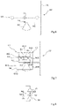
- the picture 2 is a perspective view, schematic and partial, of cell 109 of the figure 1 according to one embodiment.
- the antenna 309, the structure 307, the structure 305, the ground plane 303 and the antenna 301 are for example respectively formed in five successive metallization levels, superimposed and separated from each other by dielectric layers.
- the patch antenna 301 is intended to be placed facing the second antenna element 105b of the cell 105, while the patch antenna 309 is intended to be oriented towards the external medium.
- the level of metallization in which the antenna 301 is formed coats the upper face of the substrate 111.
- cell 109 is formed in four successive metallization levels.
- the interconnection structure 305 is then for example omitted, and the cell 109 comprises two vias extending vertically between the antenna 301 and the ground plane 303.
- a central conductor via 311 connects the antenna 301 to the antenna 309. More precisely, in the orientation of the figure 2 , the via 311 has a lower end in contact with the antenna 301 and an upper end in contact with the antenna 309. The via 311 is also connected to a central part of the structure 305. As illustrated in figure 2 , conductive vias 313a and 313b connect ends of structure 305 to ground plane 303. In addition, conductive via 315 connects antenna 309 to structure 307.
- the antenna 301, the ground plane 303, the structure 305, the structure 307 and the antenna 309 are described in more detail below in relation to figures 3 to 7 respectively.
- the picture 3 is a top view, schematic and partial, of part of the cell 109 of the figure 2 .
- the picture 3 more precisely illustrates the patch antenna 301 of the cell 109.
- the patch antenna 301 comprises a conductive plane 401 of substantially square shape inside which is formed a slot 403, or groove, in the shape of a U.
- the slot 403 is for example substantially centered with respect to to the conductive plane 401.
- the central conductive via 311 contacts, in this example, a part of the conductive plane 401 located between the two branches of the U formed by the slot 403.
- the via 311 is for example connected substantially to the center of the conductive plane 401.
- the central via 311 makes it possible to transmit to the patch antenna 309 the phase-shifted and linearly polarized signal originating from the second antenna element 105b of the cell 105 and picked up by the patch antenna 301.
- the figure 4 is a top view, schematic and partial, of another part of the cell 109 of the figure 2 .
- the figure 4 more precisely illustrates the ground plane 303 of the cell 109.
- the ground plane 303 comprises a conductive plane 501 of substantially square shape.
- the central conductor via 311 crosses the ground plane 303 approximately in the middle.
- the via 311 is isolated from the conductive plane 501 by a crown-shaped opening 503, formed in the conductive plane 501 around the via 311.
- Ground plane 303 is adapted to form electromagnetic shielding between antenna 301 and antenna 309 of cell 109.
- the vias 313a and 313b contact the conductive plane 501 in diametrically opposite regions with respect to the via 311.
- the vias 313a, 311 and 313b are located on the same line parallel to one of the sides of the conductive plane 501.
- the vias 313a and 313b are also equidistant from the via 311.
- the figure 5 is a top view, schematic and partial, of yet another part of the cell 109 of the picture 2 .
- the figure 5 more precisely illustrates the interconnect structure 305 of the cell 109.
- the structure 305 comprises a first conductive track 601a connecting the central conductor via 311 to the conductor via 313a and a second conductor track 601b connecting the central conductor via 311 to the conductor via 313b.
- Conductive tracks 601a and 601b extend for example laterally, above ground plane 303, in diametrically opposite directions from central via 311 to vias 313a and 313b, respectively.
- the tracks 601a and 601b are aligned and parallel to one of the sides of the conductive plane 501.
- the tracks 601a and 601b for example have identical lengths. More specifically, each conductive track 601a, 601b forms, for example, a quarter-wave line ( ⁇ /4), that is to say a line having a length substantially equal to a quarter of the operating wavelength of the 'antenna.
- the central conductor via 311 is connected to the ground plane 303 by the quarter-wave line 601a of the interconnection structure 305 and the via 313a on the one hand, and by the quarter-wave line 601b of the interconnection structure 305 and the via 313b on the other hand.
- the figure 6 is a top view, schematic and partial, of yet another part of the cell 109 of the picture 2 .
- the figure 6 more precisely illustrates the polarization structure 307 of the cell 109.
- the structure 307 comprises a first conductive track 701 and a second conductive track 703, perpendicular to the track 701.
- the second conductive track 703 connects the conductive track 701 to the conductive via 315.
- the conductive tracks 701 and 703 of the bias structure 307 are intended to be traversed by a bias current Ipol, for example imposed by an external DC power source, not shown.
- the structure 307 may further comprise a radio frequency decoupling element or section 705, for example in the form of a disc sector, connected to the conductive track 703.
- the radio frequency decoupling element 705 is by example produced in the same level of metallization as the conductive tracks 701 and 703 of the structure 307, near one end of the conductive track 703 connected to the via 315.
- the figure 7 is a top view, schematic and partial, of yet another part of the cell 109 of the figure 2 .
- the figure 7 more precisely illustrates the patch antenna 309 of the cell 109.
- the antenna 309 includes a conductive plane 801 with four sides.
- the conductive plane 801 is for example more precisely of rectangular shape or, as in the example illustrated in figure 7 , substantially square in shape.
- the conductive plane 801 comprises an opening 803 offset from the conductive plane 801. More precisely, in the orientation of the figure 7 , the opening 803 is eccentric with respect to a horizontal axis, separating the conductive plane 801 into two parts of substantially equivalent dimensions, and is centered on a vertical axis, separating the conductive plane 801 into two parts of substantially equivalent dimensions.
- the opening 803 has an annular shape, for example a rectangular or square annular shape.
- the opening 803 more precisely comprises first and second sides 803T, 803B (located respectively at the top and at the bottom of the opening 803, in the orientation of the figure 7 ), parallel to each other and parallel to the first and second sides 801T, 801B of the conductive plane 801, and the third and fourth sides 803L, 803R (located respectively to the left and to the right of the opening 803, in the orientation of the figure 7 ), parallel to each other and parallel to third and fourth sides 801L, 801R of the conductive plane 801.
- the sides 803T, 803B of the opening 803 are orthogonal to the sides 803L, 803R of the opening 803 and the sides 801T, 801B of the plane 801 are orthogonal to sides 801L, 801R of plane 801.
- Side 803T of opening 803 is separated from side 801T of plane 801 by a distance less than the distance separating side 803B of opening 803 from side 801B of plane 801.
- Sides 803L, 803R of opening 803 are separated from the sides respectively 801L, 801R of the plane 801 by substantially equal distances.
- the antenna 309 further comprises a terminal 805 for applying an input signal, located inside the annular opening 803. More particularly, in this example, the terminal 805 is constituted by a portion of the plane conductor 801 delimited laterally by the annular opening 803. The terminal 805 is in contact, by its lower face, with the upper end of the central conductor via 311.
- the antenna 309 further comprises a first switching element D1 connecting the terminal 805 to a first region of the plane 801 located in the vicinity of a first corner C1 of the plane 801 and a second switching element switching D2 connecting terminal 805 to a second region of plane 801 located in the vicinity of a second corner C2 of plane 801.
- switching element D1 connects terminal 805 to a first region of plane 801 located closer to the corner C1 than the other corners of the plane 801
- the switching element D2 connects the terminal 805 to a second region of the plane 801 located closer to the corner C2 than to the other corners of the plane 801.
- the corners C1 and C2 are located on the same side of plane 801. More particularly, in the example shown, corner C1 is located at the intersection of sides 801L and 801T of plane 801 and corner C2 is located at the intersection of sides 801R and 801T of the 801 plan.
- the switching elements D1 and D2 are diodes, for example PIN (Positive Intrinsic Negative) diodes, microelectromechanical switches (“Microelectromechanical switch” - MEMS, in English), varactors, phase change switches, electro-optical diodes, etc.
- PIN Positive Intrinsic Negative
- Microelectromechanical switches Microelectromechanical switch” - MEMS, in English
- varactors varactors
- phase change switches electro-optical diodes, etc.
- the conductive plane 801 of the antenna 309 is connected, by its lower face, to an upper end of the via 315.
- the via 315 thus connects the conductive plane 801 of the antenna 309 and the conductive track 703 of the polarization structure 307.
- the via 315 connects the plane 801 in a region of the plane 801 located in the vicinity of the side 803B of the opening 803.
- the via 315 is for example centered with respect to the side 803B of the opening 803.
- the figure 8 is an electrical diagram equivalent to the patch antenna 309 of the figure 7 .
- the switching elements D1 and D2 are diodes.
- Diode D1 has an anode connected to terminal 805 and a cathode connected to plane conductor 801.
- Diode D2 has an anode connected to conductor plane 801 and a cathode connected to terminal 805.
- Terminal 805 is grounded for low frequency signals and is adapted to receive the radio frequency signals picked up by antenna 301 from second antenna element 105b of cell 105 and transmitted by central conductor via 311.
- the polarization current Ipol flows in the polarization structure 307, in the via 315 and in the conductive plane 801 of the antenna 309.
- Diodes D1 and D2 are controlled in opposition, that is to say so that, if one of diodes D1, D2 is conductive, the other diode D2, D1 is blocked. Diode D1 is off and diode D2 is on when bias current Ipol is positive. In this case, a radio frequency electromagnetic field having a left circular polarization is radiated, towards the external medium, by the antenna 309. On the other hand, the diode D1 is conductive and the diode D1 is blocked when the polarization current Ipol is negative. In this case, a radiofrequency electromagnetic field having a right circular polarization is radiated, towards the external medium, by the antenna 309.
- the embodiments described are not limited to the particular case described above in which the cell 105 is a cell of the type described in the European patent EP 3392959 . More generally, the cell 105 can be constituted by any other type of cell, switchable or not, for example a cell supplying a circular polarization signal or a linear polarization signal.
- An advantage of the embodiments described is that they implement a minimum number of switches, in this case only two switches for the cell 109. This makes it possible to obtain a cell 109, therefore an antenna 100, having a simple structure, inexpensive and with good energy efficiency.
- the embodiments described make it possible to produce transmitter networks having reduced energy losses compared in particular to a case where cells having vertical and horizontal polarizations would be combined to recreate a field having circular polarization.
- the shape of the antenna 301 can be adapted according to the signal transmitted by the cell 105.
Landscapes
- Variable-Direction Aerials And Aerial Arrays (AREA)
- Waveguide Aerials (AREA)
Abstract
La présente description concerne une cellule (109) de polarisation comportant un plan conducteur rectangulaire présentant une ouverture excentrée, une borne d'application d'un signal d'entrée située à l'intérieur de l'ouverture, un premier élément de commutation reliant la borne à une première région du plan conducteur située au voisinage d'un premier coin du plan conducteur et un deuxième élément de commutation reliant la borne à une deuxième région du plan conducteur située au voisinage d'un deuxième coin du plan conducteur, les premier et deuxième coins étant reliés par un même côté du plan conducteur.The present description relates to a polarization cell (109) comprising a rectangular conductive plane having an eccentric opening, an application terminal of an input signal located inside the opening, a first switching element connecting the terminal to a first region of the conductive plane located in the vicinity of a first corner of the conductive plane and a second switching element connecting the terminal to a second region of the conductive plane located in the vicinity of a second corner of the conductive plane, the first and second corners being connected by the same side of the conductive plane.
Description
La présente description concerne de façon générale les dispositifs électroniques. La présente demande concerne plus particulièrement le domaine des antennes radio à réseau transmetteur (« transmitarray antenna », en anglais).This description relates generally to electronic devices. The present application relates more particularly to the field of radio antennas with a transmitter array (“transmitarray antenna”).
Parmi les différentes technologies d'antennes de communication radio existantes, on connaît notamment des antennes radio dites « à réseau transmetteur ». Ces antennes comprennent généralement plusieurs cellules élémentaires comportant chacune un premier élément d'antenne irradié par un champ électromagnétique émis par une ou plusieurs sources et un deuxième élément d'antenne transmettant un signal modifié vers l'extérieur de l'antenne.Among the different technologies of existing radio communication antennas, radio antennas called “transmitter network” are known in particular. These antennas generally comprise several elementary cells each comprising a first antenna element irradiated by an electromagnetic field emitted by one or more sources and a second antenna element transmitting a modified signal to the outside of the antenna.
Pour des applications, par exemple telles que la communication satellite (« satellite communication » ou « SatCom », en anglais), il serait souhaitable de disposer d'antennes à réseau transmetteur reconfigurables permettant de modifier, de façon dynamique, la polarisation de l'onde rayonnée.For applications, for example such as satellite communication ("satellite communication" or "SatCom", in English), it would be desirable to have reconfigurable transmitter array antennas making it possible to dynamically modify the polarization of the radiated wave.
Il existe un besoin d'améliorer les antennes à réseau transmetteur existantes.There is a need to improve existing transmitter array antennas.
Un mode de réalisation pallie tout ou partie des inconvénients des antennes à réseau transmetteur connues.One embodiment overcomes all or part of the drawbacks of known transmitter array antennas.
Un mode de réalisation prévoit une cellule de polarisation comportant un plan conducteur rectangulaire présentant une ouverture excentrée, une borne d'application d'un signal d'entrée située à l'intérieur de l'ouverture, un premier élément de commutation reliant la borne à une première région du plan conducteur située au voisinage d'un premier coin du plan conducteur et un deuxième élément de commutation reliant la borne à une deuxième région du plan conducteur située au voisinage d'un deuxième coin du plan conducteur, les premier et deuxième coins étant reliés par un même côté du plan conducteur.One embodiment provides a bias cell comprising a rectangular conductive plane having an off-center opening, a terminal for applying an input signal located inside the opening, a first switching element connecting the terminal to a first region of the conductive plane located in the vicinity of a first corner of the conductive plane and a second switching element connecting the terminal to a second region of the conductive plane located in the vicinity of a second corner of the conductive plane, the first and second corners being connected by the same side of the conductive plane.
Selon un mode de réalisation, la borne est connectée à un plan de masse.According to one embodiment, the terminal is connected to a ground plane.
Selon un mode de réalisation, la borne est située au centre de l'ouverture.According to one embodiment, the terminal is located in the center of the opening.
Selon un mode de réalisation, l'ouverture est plus proche dudit côté du plan conducteur que d'un autre côté du plan conducteur opposé audit côté.According to one embodiment, the opening is closer to said side of the conductive plane than to another side of the conductive plane opposite said side.
Selon un mode de réalisation, la cellule comporte en outre une antenne à plaque adaptée à transmettre le signal d'entrée à la borne.According to one embodiment, the cell further comprises a patch antenna suitable for transmitting the input signal to the terminal.
Selon un mode de réalisation, le plan conducteur est adapté à recevoir un signal de commande des premier et deuxième éléments de commutation.According to one embodiment, the conductive plane is adapted to receive a control signal from the first and second switching elements.
Selon un mode de réalisation, le premier élément de commutation est une diode PIN comportant une anode connectée à la borne et une cathode connectée au plan conducteur et le deuxième élément de commutation est une autre diode PIN comportant une anode connectée au plan conducteur et une cathode connectée à la borne.According to one embodiment, the first switching element is a PIN diode comprising an anode connected to the terminal and a cathode connected to the conductive plane and the second switching element is another PIN diode comprising an anode connected to the conductive plane and a cathode connected to the terminal.
Un mode de réalisation prévoit une cellule d'antenne comportant une cellule de polarisation telle que décrite et une cellule de transmission adaptée à commuter entre au moins deux états de phase.One embodiment provides an antenna cell comprising a polarization cell as described and a transmission cell capable of switching between at least two phase states.
Selon un mode de réalisation, la cellule de transmission est adaptée à commuter entre quatre états de phase.According to one embodiment, the transmission cell is adapted to switch between four phase states.
Selon un mode de réalisation, la cellule de polarisation et la cellule de transmission sont isolées l'une de l'autre par un substrat diélectrique.According to one embodiment, the bias cell and the transmission cell are isolated from each other by a dielectric substrate.
Un mode de réalisation prévoit une antenne comprenant un réseau de cellules d'antenne telles que décrites.One embodiment provides an antenna comprising an array of antenna cells as described.
Selon un mode de réalisation, l'antenne comprend en outre au moins une source configurée pour irradier une face du réseau.According to one embodiment, the antenna further comprises at least one source configured to irradiate one face of the array.
Ces caractéristiques et avantages, ainsi que d'autres, seront exposés en détail dans la description suivante de modes de réalisation particuliers faite à titre non limitatif en relation avec les figures jointes parmi lesquelles :
- la
figure 1 est une vue de côté schématique d'un exemple d'antenne à réseau transmetteur du type auquel s'appliquent, à titre d'exemple, les modes de réalisation décrits ; - la
figure 2 est une vue en perspective, schématique et partielle, d'une cellule de lafigure 1 selon un mode de réalisation ; - la
figure 3 est une vue de dessus, schématique et partielle, d'une partie de la cellule de lafigure 2 ; - la
figure 4 est une vue de dessus, schématique et partielle, d'une autre partie de la cellule de lafigure 2 ; - la
figure 5 est une vue de dessus, schématique et partielle, d'encore une autre partie de la cellule de lafigure 2 ; - la
figure 6 est une vue de dessus, schématique et partielle, d'encore une autre partie de la cellule de lafigure 2 ; - la
figure 7 est une vue de dessus, schématique et partielle, d'encore une autre partie de la cellule de lafigure 2 ; et - la
figure 8 est un schéma électrique équivalent à la partie de cellule de lafigure 7 .
- the
figure 1 is a schematic side view of an example of a transmitter array antenna of the type to which the described embodiments apply, by way of example; - the
figure 2 is a perspective view, schematic and partial, of a cell of thefigure 1 according to one embodiment; - the
picture 3 is a top view, schematic and partial, of part of the cell of thefigure 2 ; - the
figure 4 is a top view, schematic and partial, of another part of the cell of thepicture 2 ; - the
figure 5 is a schematic partial top view of yet another portion of the cell of thepicture 2 ; - the
figure 6 is a schematic partial top view of yet another portion of the cell of thepicture 2 ; - the
figure 7 is a schematic partial top view of yet another portion of the cell of thepicture 2 ; and - the
figure 8 is an electrical diagram equivalent to the cell part of thefigure 7 .
De mêmes éléments ont été désignés par de mêmes références dans les différentes figures. En particulier, les éléments structurels et/ou fonctionnels communs aux différents modes de réalisation peuvent présenter les mêmes références et peuvent disposer de propriétés structurelles, dimensionnelles et matérielles identiques.The same elements have been designated by the same references in the various figures. In particular, the structural and/or functional elements common to the various embodiments may have the same references and may have identical structural, dimensional and material properties.
Par souci de clarté, seuls les étapes et éléments utiles à la compréhension des modes de réalisation décrits ont été représentés et sont détaillés. En particulier, on va décrire ci-après des modes de réalisation d'une cellule pour antenne à réseau transmetteur. La structure et le fonctionnement de la ou des sources primaires de l'antenne, destinées à irradier le réseau transmetteur, ne seront toutefois pas détaillés, les modes de réalisation décrits étant compatibles avec toutes ou la plupart des sources primaires d'irradiation pour antenne à réseau transmetteur connues. À titre d'exemple, chaque source primaire est adaptée à produire un faisceau de forme générale conique irradiant tout ou partie du réseau transmetteur. Chaque source primaire comprend par exemple une antenne cornet. À titre d'exemple, l'axe central de chaque source primaire est sensiblement orthogonal au plan moyen du réseau.For the sake of clarity, only the steps and elements useful for understanding the embodiments described have been represented and are detailed. In particular, embodiments of a cell for an antenna with a transmitter array will be described below. The structure and operation of the primary source or sources of the antenna, intended to irradiate the transmitter network, will however not be detailed, the embodiments described being compatible with all or most of the primary irradiation sources for antenna with known transmitter network. By way of example, each primary source is adapted to produce a beam of generally conical shape irradiating all or part of the transmitter network. Each primary source comprises for example a horn antenna. By way of example, the central axis of each primary source is substantially orthogonal to the mean plane of the network.
Par ailleurs, les procédés de fabrication des réseaux transmetteurs décrits ne seront pas détaillés, la réalisation des structures décrites étant à la portée de la personne du métier à partir des indications de la présente description, par exemple en mettant en œuvre des techniques usuelles de fabrication de circuits imprimés.Furthermore, the manufacturing methods of the transmitter networks described will not be detailed, the realization of the described structures being within the reach of the person skilled in the art from the indications of the present description, for example by implementing usual manufacturing techniques. of printed circuits.
Sauf précision contraire, lorsque l'on fait référence à deux éléments connectés entre eux, cela signifie directement connectés sans éléments intermédiaires autres que des conducteurs, et lorsque l'on fait référence à deux éléments reliés (en anglais "coupled") entre eux, cela signifie que ces deux éléments peuvent être connectés ou être reliés par l'intermédiaire d'un ou plusieurs autres éléments.Unless otherwise specified, when reference is made to two elements connected together, this means directly connected without intermediate elements other than conductors, and when reference is made to two elements connected (in English "coupled") between them, this means that these two elements can be connected or be linked through one or more other elements.
Dans la description qui suit, lorsque l'on fait référence à des qualificatifs de position absolue, tels que les termes "avant", "arrière", "haut", "bas", "gauche", "droite", etc., ou relative, tels que les termes "dessus", "dessous", "supérieur", "inférieur", etc., ou à des qualificatifs d'orientation, tels que les termes "horizontal", "vertical", etc., il est fait référence sauf précision contraire à l'orientation des figures.In the following description, when referring to absolute position qualifiers, such as "front", "rear", "up", "down", "left", "right", etc., or relative, such as the terms "above", "below", "upper", "lower", etc., or to qualifiers of orientation, such as the terms "horizontal", "vertical", etc., it reference is made unless otherwise specified to the orientation of the figures.
Sauf précision contraire, les expressions "environ", "approximativement", "sensiblement", et "de l'ordre de" signifient à 10 % près, de préférence à 5 % près.Unless specified otherwise, the expressions “about”, “approximately”, “substantially”, and “of the order of” mean to within 10%, preferably within 5%.
La
L'antenne 100 comprend typiquement une ou plusieurs sources primaires 101 (une unique source 101, dans l'exemple représenté) irradiant un réseau transmetteur 103. La source 101 peut présenter une polarisation quelconque, par exemple linéaire ou circulaire. Le réseau 103 comprend une pluralité de cellules élémentaires 105, par exemple disposées en matrice selon des lignes et des colonnes. Chaque cellule 105 comprend typiquement un premier élément d'antenne 105a, situé du côté d'une première face du réseau 103 disposée en regard de la source primaire 101, et un deuxième élément d'antenne 105b, situé du côté d'une deuxième face du réseau opposée à la première face. La deuxième face du réseau 103 est par exemple tournée vers un milieu d'émission de l'antenne 100.The
Chaque cellule 105 est apte, en émission, à recevoir un rayonnement électromagnétique sur son premier élément d'antenne 105a et à réémettre ce rayonnement depuis son deuxième élément d'antenne 105b, par exemple en introduisant un déphasage φ connu.Each
Dans l'exemple représenté, l'antenne 100 comporte en outre un réseau de polarisation 107. Le réseau 107 comprend une pluralité de cellules élémentaires 109, par exemple disposées en matrice selon des lignes et des colonnes. Dans cet exemple, le nombre de cellules élémentaires de polarisation 109 du réseau de polarisation 107 est identique au nombre de cellules élémentaires de transmission 105 du réseau transmetteur 103. Les cellules 109 du réseau 107 sont par exemple, comme illustré en
Chaque cellule 109 comprend par exemple un premier élément d'antenne 109a, situé du côté d'une première face du réseau 107 disposée en regard des deuxièmes éléments d'antenne 105b des cellules 105, et un deuxième élément d'antenne 109b, situé du côté d'une deuxième face du réseau 107 opposée à la première face. La deuxième face du réseau 107 est par exemple tournée vers un milieu d'émission de l'antenne 100.Each
Chaque cellule 109 est apte, en émission, à recevoir sur son premier élément d'antenne 109a un rayonnement électromagnétique en provenance de la cellule 105 associée et à réémettre, depuis son deuxième élément d'antenne 109b, un rayonnement présentant une polarisation circulaire (POL). Les cellules élémentaires 109 peuvent en outre être commandées électroniquement, de façon individuelle, afin de modifier le sens de polarisation circulaire du rayonnement émis.Each
Dans l'exemple représenté, les deuxièmes éléments d'antenne 105b des cellules 105 sont isolés des premiers éléments d'antenne 109a des cellules 109 situées en vis-à-vis par un substrat 111 en un matériau diélectrique. Les cellules 109 sont ainsi dépourvues de toute liaison ou connexion électrique avec les cellules 105. Dans l'orientation de la
À titre de variante, le substrat 111 peut être omis, les cellules 105 et 109 étant alors par exemple séparées l'une de l'autre par un volume d'air.As a variant, the substrate 111 can be omitted, the
Dans l'exemple illustré en
La cellule 105 permet par exemple de commuter entre plusieurs valeurs du déphasage φ à appliquer au rayonnement électromagnétique émis par la source 101. À titre d'exemple, la cellule 105 est du type décrit dans le brevet européen
À titre d'exemple, le rayonnement électromagnétique présente, en entrée et en sortie de la cellule 105, une polarisation linéaire.By way of example, the electromagnetic radiation has, at the input and at the output of the
Selon un mode de réalisation, la cellule 109 est adaptée à capter le rayonnement déphasé et polarisé linéairement émis par la cellule 105 et à réémettre un rayonnement présentant une polarisation circulaire. La cellule 109 permet en outre de commuter entre deux états ou sens de polarisation circulaire, respectivement droite (sens horaire, du point de vue de la source 101) et gauche (sens anti-horaire, du point de vue de la source 101).According to one embodiment, the
Ainsi, dans l'exemple de l'antenne 100 illustrée en
Les caractéristiques du faisceau produit par l'antenne 100, notamment sa forme (ou gabarit) et sa direction d'émission maximale (ou direction de pointage), dépendent des valeurs des déphasages respectivement introduits par les différentes cellules 105 du réseau 103.The characteristics of the beam produced by the
Les antennes à réseau transmetteur ont pour avantages, entre autres, de présenter une bonne efficacité énergétique et d'être relativement simples, peu onéreuses et peu encombrantes. Cela provient notamment du fait que les réseaux transmetteurs sont réalisables en technologie planaire, généralement sur circuit imprimé.Transmitter array antennas have the advantages, among others, of having good energy efficiency and of being relatively simple, inexpensive and compact. This stems in particular from the fact that the transmitting networks can be produced using planar technology, generally on a printed circuit.
On s'intéresse ici plus particulièrement aux antennes à réseau transmetteur 103 reconfigurable. Le réseau transmetteur 103 est dit reconfigurable lorsque les cellules élémentaires 105 sont commandables électroniquement de façon individuelle pour modifier leur valeur de déphasage φ, ce qui permet de modifier dynamiquement les caractéristiques du faisceau généré par l'antenne, et notamment de modifier sa direction de pointage sans déplacer mécaniquement l'antenne ou une partie de l'antenne au moyen d'un élément motorisé.We are particularly interested here in the antennas with a
La
Selon ce mode de réalisation, la cellule 109 comporte :
- une première antenne à plaque 301 (« patch antenna », en anglais) adaptée à capter le rayonnement électromagnétique émis par le deuxième élément d'antenne 105b de la cellule 105 ;
- un plan de masse 303 ;
une structure 305 d'interconnexion ;une structure 307 de polarisation ; et- une deuxième antenne à
plaque 309, faisant partie du deuxième élément d'antenne 109b de la cellule 109, adaptée à émettre un rayonnement électromagnétique présentant une polarisation circulaire gauche ou droite.
- a
first patch antenna 301 adapted to pick up the electromagnetic radiation emitted by thesecond antenna element 105b of thecell 105; - a
ground plane 303; - an
interconnect structure 305; - a
bias structure 307; and - a
second patch antenna 309, forming part of thesecond antenna element 109b of thecell 109, adapted to emit electromagnetic radiation having a left or right circular polarization.
L'antenne 309, la structure 307, la structure 305, le plan de masse 303 et l'antenne 301 sont par exemple respectivement formés dans cinq niveaux de métallisation successifs, superposés et séparés les uns des autres par des couches diélectriques. L'antenne à plaque 301 est destinée à être placée en regard du deuxième élément d'antenne 105b de la cellule 105, tandis que l'antenne à plaque 309 est destinée à être orientée vers le milieu extérieur. À titre d'exemple, le niveau de métallisation dans lequel est formée l'antenne 301 revêt la face supérieure du substrat 111.The
À titre de variante, la cellule 109 est formée dans quatre niveaux de métallisation successifs. La structure 305 d'interconnexion est alors par exemple omise, et la cellule 109 comporte deux vias s'étendant verticalement entre l'antenne 301 et le plan de masse 303.Alternatively,
Dans l'exemple représenté, un via conducteur central 311 connecte l'antenne 301 à l'antenne 309. Plus précisément, dans l'orientation de la
L'antenne 301, le plan de masse 303, la structure 305, la structure 307 et l'antenne 309 sont décrits plus en détail ci-dessous en relation avec les figures respectivement 3 à 7.The
La
Dans l'exemple représenté, l'antenne à plaque 301 comporte un plan conducteur 401 de forme sensiblement carrée à l'intérieur duquel est formée une fente 403, ou rainure, en forme de U. La fente 403 est par exemple sensiblement centrée par rapport au plan conducteur 401. Le via conducteur central 311 contacte, dans cet exemple, une partie du plan conducteur 401 située entre les deux branches du U formé par la fente 403. Le via 311 est par exemple connecté sensiblement au centre du plan conducteur 401.In the example represented, the
Le via central 311 permet de transmettre à l'antenne à plaque 309 le signal déphasé et polarisé linéairement provenant du deuxième élément d'antenne 105b de la cellule 105 et capté par l'antenne à plaque 301.The central via 311 makes it possible to transmit to the
La
Dans l'exemple représenté, le plan de masse 303 comporte un plan conducteur 501 de forme sensiblement carrée. Dans cet exemple, le via conducteur central 311 traverse le plan de masse 303 approximativement en son milieu. Le via 311 est isolé du plan conducteur 501 par une ouverture 503 en forme de couronne, formée dans le plan conducteur 501 autour du via 311.In the example represented, the
Le plan de masse 303 est adapté à former un blindage électromagnétique entre l'antenne 301 et l'antenne 309 de la cellule 109.
Dans l'exemple illustré en
La
Dans l'exemple représenté, la structure 305 comporte une première piste conductrice 601a connectant le via conducteur central 311 au via conducteur 313a et une deuxième piste conductrice 601b connectant le via conducteur central 311 au via conducteur 313b. Les pistes conductrices 601a et 601b s'étendent par exemple latéralement, au-dessus du plan de masse 303, dans des directions diamétralement opposées depuis le via central 311 jusqu'aux vias 313a et 313b, respectivement. Dans cet exemple, les pistes 601a et 601b sont alignées et parallèles à l'un des côtés du plan conducteur 501. Les pistes 601a et 601b présentent par exemple des longueurs identiques. Plus précisément, chaque piste conductrice 601a, 601b forme par exemple une ligne quart d'onde (λ/4), c'est-à-dire une ligne présentant une longueur sensiblement égale au quart de la longueur d'onde de fonctionnement de l'antenne.In the example represented, the
Dans l'exemple représenté, le via conducteur central 311 est connecté au plan de masse 303 par la ligne quart d'onde 601a de la structure d'interconnexion 305 et le via 313a d'une part, et par la ligne quart d'onde 601b de la structure d'interconnexion 305 et le via 313b d'autre part.In the example shown, the central conductor via 311 is connected to the
La
Dans l'exemple représenté, la structure 307 comporte une première piste conductrice 701 et une deuxième piste conductrice 703, perpendiculaire à la piste 701. La deuxième piste conductrice 703 connecte la piste conductrice 701 au via conducteur 315. Les pistes conductrices 701 et 703 de la structure de polarisation 307 sont destinées à être parcourues par un courant Ipol de polarisation, par exemple imposé par une source d'alimentation continue externe non représentée.In the example represented, the
Comme illustré en
La
Selon un mode de réalisation, l'antenne 309 comporte un plan conducteur 801 à quatre côtés. Le plan conducteur 801 est par exemple plus précisément de forme rectangulaire ou, comme dans l'exemple illustré en
Selon ce mode de réalisation, le plan conducteur 801 comporte une ouverture 803 excentrée par rapport au plan conducteur 801. Plus précisément, dans l'orientation de la
Dans cet exemple, l'ouverture 803 présente une forme annulaire, par exemple une forme annulaire rectangulaire ou carrée. L'ouverture 803 comporte plus précisément des premier et deuxième côtés 803T, 803B (situés respectivement en haut et en bas de l'ouverture 803, dans l'orientation de la
Le côté 803T de l'ouverture 803 est séparé du côté 801T du plan 801 par une distance inférieure à la distance séparant le côté 803B de l'ouverture 803 du côté 801B du plan 801. Les côtés 803L, 803R de l'ouverture 803 sont séparés des côtés respectivement 801L, 801R du plan 801 par des distances sensiblement égales.
L'antenne 309 comporte en outre une borne 805 d'application d'un signal d'entrée, située à l'intérieur de l'ouverture annulaire 803. Plus particulièrement, dans cet exemple, la borne 805 est constituée par une portion du plan conducteur 801 délimitée latéralement par l'ouverture annulaire 803. La borne 805 est en contact, par sa face inférieure, avec l'extrémité supérieure du via conducteur central 311.The
Selon un mode de réalisation, l'antenne 309 comporte en outre un premier élément de commutation D1 reliant la borne 805 à une première région du plan 801 située au voisinage d'un premier coin C1 du plan 801 et un deuxième élément de commutation D2 reliant la borne 805 à une deuxième région du plan 801 située au voisinage d'un deuxième coin C2 du plan 801. Autrement dit, l'élément de commutation D1 relie la borne 805 à une première région du plan 801 située plus proche du coin C1 que des autres coins du plan 801, et l'élément de commutation D2 relie la borne 805 à une deuxième région du plan 801 située plus proche du coin C2 que des autres coins du plan 801. Dans cet exemple, les coins C1 et C2 sont situés sur un même côté du plan 801. Plus particulièrement, dans l'exemple représenté, le coin C1 est situé à l'intersection des côtés 801L et 801T du plan 801 et le coin C2 est situé à l'intersection des côtés 801R et 801T du plan 801.According to one embodiment, the
À titre d'exemple, les éléments de commutation D1 et D2 sont des diodes, par exemple des diodes PIN (de l'anglais « Positive Intrinsic Negative »), des commutateurs micro électromécaniques (« Microelectromechanical switch » - MEMS, en anglais), des varactors, des commutateurs à changement de phase, des diodes électro-optiques, etc.By way of example, the switching elements D1 and D2 are diodes, for example PIN (Positive Intrinsic Negative) diodes, microelectromechanical switches (“Microelectromechanical switch” - MEMS, in English), varactors, phase change switches, electro-optical diodes, etc.
Dans l'exemple représenté, le plan conducteur 801 de l'antenne 309 est connecté, par sa face inférieure, à une extrémité supérieure du via 315. Le via 315 connecte ainsi le plan conducteur 801 de l'antenne 309 et la piste conductrice 703 de la structure de polarisation 307. Dans cet exemple, le via 315 connecte le plan 801 dans une région du plan 801 située au voisinage du côté 803B de l'ouverture 803. Le via 315 est par exemple centré par rapport au côté 803B de l'ouverture 803.In the example represented, the
La
Dans l'exemple représenté, les éléments de commutation D1 et D2 sont des diodes. La diode D1 comporte une anode connectée à la borne 805 et une cathode connectée au plan conducteur 801. La diode D2 comporte une anode connectée au plan conducteur 801 et une cathode connectée à la borne 805.In the example represented, the switching elements D1 and D2 are diodes. Diode D1 has an anode connected to
La borne 805 est mise à la masse pour les signaux basse fréquence et est adaptée à recevoir les signaux radiofréquence captés par l'antenne 301 en provenance du deuxième élément d'antenne 105b de la cellule 105 et transmis par le via conducteur central 311. Le courant Ipol de polarisation circule dans la structure de polarisation 307, dans le via 315 et dans le plan conducteur 801 de l'antenne 309.
Les diodes D1 et D2 sont commandées en opposition, c'est-à-dire de sorte que, si l'une des diodes D1, D2 est passante, l'autre diode D2, D1 soit bloquée. La diode D1 est bloquée et la diode D2 est passante lorsque le courant Ipol de polarisation est positif. Dans ce cas, un champ électromagnétique radiofréquence présentant une polarisation circulaire gauche est rayonné, vers le milieu extérieur, par l'antenne 309. En revanche, la diode D1 est passante et la diode D1 est bloquée lorsque le courant Ipol de polarisation est négatif. Dans ce cas, un champ électromagnétique radiofréquence présentant une polarisation circulaire droite est rayonné, vers le milieu extérieur, par l'antenne 309.Diodes D1 and D2 are controlled in opposition, that is to say so that, if one of diodes D1, D2 is conductive, the other diode D2, D1 is blocked. Diode D1 is off and diode D2 is on when bias current Ipol is positive. In this case, a radio frequency electromagnetic field having a left circular polarization is radiated, towards the external medium, by the
En commandant le niveau du signal Ipol, on peut ainsi avantageusement obtenir, en sortie de l'élément d'antenne 109b de la cellule 109, deux états de polarisation circulaire (gauche et droite). Lorsque la cellule 109 est couplée à la cellule 105 du type décrit dans le brevet européen
Les modes de réalisation décrits ne se limitent pas au cas particulier décrit ci-dessus dans lequel la cellule 105 est une cellule du type décrit dans le brevet européen
Un avantage des modes de réalisation décrits tient au fait qu'ils mettent en œuvre un nombre minimal de commutateurs, en l'espèce seulement deux commutateurs pour la cellule 109. Cela permet d'obtenir une cellule 109, donc une antenne 100, présentant une structure simple, peu coûteuse et présentant un bon rendement énergétique. En particulier, les modes de réalisation décrits permettent de réaliser des réseaux transmetteurs présentant des pertes énergétiques réduites par rapport notamment à un cas où l'on combinerait des cellules présentant des polarisations verticale et horizontale pour recréer un champ présentant une polarisation circulaire.An advantage of the embodiments described is that they implement a minimum number of switches, in this case only two switches for the
Divers modes de réalisation et variantes ont été décrits. La personne du métier comprendra que certaines caractéristiques de ces divers modes de réalisation et variantes pourraient être combinées, et d'autres variantes apparaîtront à la personne du métier. En particulier, la forme de l'antenne 301 peut être adaptée en fonction du signal transmis par la cellule 105.Various embodiments and variants have been described. Those skilled in the art will understand that certain features of these various embodiments and variations could be combined, and other variations will occur to those skilled in the art. In particular, the shape of the
Enfin, la mise en œuvre pratique des modes de réalisation et variantes décrits est à la portée de la personne du métier à partir des indications fonctionnelles données ci-dessus. En particulier, les niveaux du signal Ipol de commande des commutateurs D1 et D2 peuvent être adaptés par la personne du métier en fonction de l'application.Finally, the practical implementation of the embodiments and variants described is within the abilities of those skilled in the art based on the functional indications given above. In particular, the levels of the control signal Ipol of the switches D1 and D2 can be adapted by the person skilled in the art according to the application.
Claims (12)
Applications Claiming Priority (1)
| Application Number | Priority Date | Filing Date | Title |
|---|---|---|---|
| FR2107335A FR3125173A1 (en) | 2021-07-07 | 2021-07-07 | Transmitter array antenna cell |
Publications (1)
| Publication Number | Publication Date |
|---|---|
| EP4117117A1 true EP4117117A1 (en) | 2023-01-11 |
Family
ID=77711046
Family Applications (1)
| Application Number | Title | Priority Date | Filing Date |
|---|---|---|---|
| EP22181429.6A Pending EP4117117A1 (en) | 2021-07-07 | 2022-06-28 | Antenna cell with transmitter network |
Country Status (3)
| Country | Link |
|---|---|
| US (1) | US11962094B2 (en) |
| EP (1) | EP4117117A1 (en) |
| FR (1) | FR3125173A1 (en) |
Families Citing this family (1)
| Publication number | Priority date | Publication date | Assignee | Title |
|---|---|---|---|---|
| FR3135572A1 (en) | 2022-05-11 | 2023-11-17 | Commissariat A L'energie Atomique Et Aux Energies Alternatives | LOW PROFILE ANTENNA WITH TWO-DIMENSIONAL ELECTRONIC SCANNING |
Citations (2)
| Publication number | Priority date | Publication date | Assignee | Title |
|---|---|---|---|---|
| EP3392959A1 (en) | 2017-04-14 | 2018-10-24 | Commissariat A L'energie Atomique Et Aux Energies Alternatives | Elementary cell of a transmitter network for a reconfigurable antenna |
| EP3764462A1 (en) * | 2018-08-24 | 2021-01-13 | Samsung Electronics Co., Ltd. | Antenna device for beam steering and focusing |
Family Cites Families (4)
| Publication number | Priority date | Publication date | Assignee | Title |
|---|---|---|---|---|
| FR2969832B1 (en) * | 2010-12-24 | 2013-01-18 | Commissariat Energie Atomique | RADIATION CELL WITH TWO PHASE STATES FOR TRANSMITTER NETWORK |
| TWI563804B (en) * | 2015-01-21 | 2016-12-21 | Wistron Neweb Corp | Microstrip antenna transceiver |
| FR3039711B1 (en) * | 2015-07-28 | 2017-12-29 | Commissariat Energie Atomique | ELEMENTARY CELL OF A TRANSMITTER NETWORK FOR A RECONFIGURABLE ANTENNA. |
| US20220199556A1 (en) * | 2020-12-23 | 2022-06-23 | Intel Corporation | Package system and package |
-
2021
- 2021-07-07 FR FR2107335A patent/FR3125173A1/en active Pending
-
2022
- 2022-06-27 US US17/809,049 patent/US11962094B2/en active Active
- 2022-06-28 EP EP22181429.6A patent/EP4117117A1/en active Pending
Patent Citations (2)
| Publication number | Priority date | Publication date | Assignee | Title |
|---|---|---|---|---|
| EP3392959A1 (en) | 2017-04-14 | 2018-10-24 | Commissariat A L'energie Atomique Et Aux Energies Alternatives | Elementary cell of a transmitter network for a reconfigurable antenna |
| EP3764462A1 (en) * | 2018-08-24 | 2021-01-13 | Samsung Electronics Co., Ltd. | Antenna device for beam steering and focusing |
Also Published As
| Publication number | Publication date |
|---|---|
| US20230010547A1 (en) | 2023-01-12 |
| FR3125173A1 (en) | 2023-01-13 |
| US11962094B2 (en) | 2024-04-16 |
Similar Documents
| Publication | Publication Date | Title |
|---|---|---|
| EP3392959B1 (en) | Elementary cell of a transmitter network for a reconfigurable antenna | |
| CA2053643C (en) | Double polarization radiating element feeding device | |
| EP0089084B1 (en) | Flat microwave antenna structure | |
| EP2656438B1 (en) | Radio cell with two phase states for transmit array | |
| EP0108463B1 (en) | Radiating element for cross-polarized microwave signals and planar antenna consisting of an array of such elements | |
| FR3039711A1 (en) | ELEMENTARY CELL OF A TRANSMITTER NETWORK FOR A RECONFIGURABLE ANTENNA. | |
| EP0627783A1 (en) | Radiating multi-layer structure with variable directivity | |
| EP0064313A1 (en) | Circularly polarised microwave radiating element and flat microwave antenna using an array of such elements | |
| EP0667984B1 (en) | Monopolar wire-plate antenna | |
| CA2869648A1 (en) | Compact, polarizing power distributor, network of several distributors, compact radiating element and flat antenna comprising such a distributor | |
| FR2975537A1 (en) | RADIANT ELEMENT FOR AN ACTIVE NETWORK ANTENNA CONSISTING OF BASIC TILES | |
| FR2863110A1 (en) | ANTENNA IN MULTI-BAND NETWORK WITH DOUBLE POLARIZATION | |
| EP4117117A1 (en) | Antenna cell with transmitter network | |
| EP0518271A1 (en) | Elemental microwave antenna with two polarisations | |
| EP1234356B1 (en) | Active electronic scan microwave reflector | |
| EP4087060A1 (en) | Antenna cell with transmitter network | |
| WO2002011238A1 (en) | Active dual-polarization microwave reflector, in particular for electronically scanning antenna | |
| FR2831734A1 (en) | DEVICE FOR RECEIVING AND / OR TRANSMITTING RADIATION DIVERSITY ELECTROMAGNETIC SIGNALS | |
| CA2808511C (en) | Flat antenna for a terminal operating in dual circular polarisation, airborne terminal and satellite telecommunication system featuring at least one antenna | |
| EP3840122A1 (en) | Elementary cell of a transmitter array | |
| FR2965112A1 (en) | MULTI-LAYER CIRCUIT BROADBAND SYMETRISER FOR NETWORK ANTENNA | |
| EP0993073A1 (en) | Panel of active antennas with multilayer structure | |
| EP4350890A1 (en) | Phase change material based switch | |
| WO2023218008A1 (en) | Low-profile antenna with two-dimensional electronic scanning | |
| FR3123513A1 (en) | Stack for manufacturing an integrated circuit intended to provide an electromagnetic lens function for a reconfigurable antenna with a transmitter array |
Legal Events
| Date | Code | Title | Description |
|---|---|---|---|
| PUAI | Public reference made under article 153(3) epc to a published international application that has entered the european phase |
Free format text: ORIGINAL CODE: 0009012 |
|
| STAA | Information on the status of an ep patent application or granted ep patent |
Free format text: STATUS: REQUEST FOR EXAMINATION WAS MADE |
|
| 17P | Request for examination filed |
Effective date: 20220628 |
|
| AK | Designated contracting states |
Kind code of ref document: A1 Designated state(s): AL AT BE BG CH CY CZ DE DK EE ES FI FR GB GR HR HU IE IS IT LI LT LU LV MC MK MT NL NO PL PT RO RS SE SI SK SM TR |