EP3392959A1 - Elementary cell of a transmitter network for a reconfigurable antenna - Google Patents
Elementary cell of a transmitter network for a reconfigurable antenna Download PDFInfo
- Publication number
- EP3392959A1 EP3392959A1 EP18166901.1A EP18166901A EP3392959A1 EP 3392959 A1 EP3392959 A1 EP 3392959A1 EP 18166901 A EP18166901 A EP 18166901A EP 3392959 A1 EP3392959 A1 EP 3392959A1
- Authority
- EP
- European Patent Office
- Prior art keywords
- elementary cell
- antenna
- phase shift
- dielectric substrate
- shift circuit
- Prior art date
- Legal status (The legal status is an assumption and is not a legal conclusion. Google has not performed a legal analysis and makes no representation as to the accuracy of the status listed.)
- Granted
Links
Images

Classifications
-
- H—ELECTRICITY
- H01—ELECTRIC ELEMENTS
- H01Q—ANTENNAS, i.e. RADIO AERIALS
- H01Q3/00—Arrangements for changing or varying the orientation or the shape of the directional pattern of the waves radiated from an antenna or antenna system
- H01Q3/26—Arrangements for changing or varying the orientation or the shape of the directional pattern of the waves radiated from an antenna or antenna system varying the relative phase or relative amplitude of energisation between two or more active radiating elements; varying the distribution of energy across a radiating aperture
- H01Q3/30—Arrangements for changing or varying the orientation or the shape of the directional pattern of the waves radiated from an antenna or antenna system varying the relative phase or relative amplitude of energisation between two or more active radiating elements; varying the distribution of energy across a radiating aperture varying the relative phase between the radiating elements of an array
- H01Q3/34—Arrangements for changing or varying the orientation or the shape of the directional pattern of the waves radiated from an antenna or antenna system varying the relative phase or relative amplitude of energisation between two or more active radiating elements; varying the distribution of energy across a radiating aperture varying the relative phase between the radiating elements of an array by electrical means
-
- H—ELECTRICITY
- H01—ELECTRIC ELEMENTS
- H01Q—ANTENNAS, i.e. RADIO AERIALS
- H01Q1/00—Details of, or arrangements associated with, antennas
- H01Q1/12—Supports; Mounting means
- H01Q1/22—Supports; Mounting means by structural association with other equipment or articles
- H01Q1/2283—Supports; Mounting means by structural association with other equipment or articles mounted in or on the surface of a semiconductor substrate as a chip-type antenna or integrated with other components into an IC package
-
- H—ELECTRICITY
- H01—ELECTRIC ELEMENTS
- H01Q—ANTENNAS, i.e. RADIO AERIALS
- H01Q1/00—Details of, or arrangements associated with, antennas
- H01Q1/48—Earthing means; Earth screens; Counterpoises
-
- H—ELECTRICITY
- H01—ELECTRIC ELEMENTS
- H01Q—ANTENNAS, i.e. RADIO AERIALS
- H01Q15/00—Devices for reflection, refraction, diffraction or polarisation of waves radiated from an antenna, e.g. quasi-optical devices
- H01Q15/24—Polarising devices; Polarisation filters
-
- H—ELECTRICITY
- H01—ELECTRIC ELEMENTS
- H01Q—ANTENNAS, i.e. RADIO AERIALS
- H01Q21/00—Antenna arrays or systems
- H01Q21/0087—Apparatus or processes specially adapted for manufacturing antenna arrays
- H01Q21/0093—Monolithic arrays
-
- H—ELECTRICITY
- H01—ELECTRIC ELEMENTS
- H01Q—ANTENNAS, i.e. RADIO AERIALS
- H01Q3/00—Arrangements for changing or varying the orientation or the shape of the directional pattern of the waves radiated from an antenna or antenna system
- H01Q3/44—Arrangements for changing or varying the orientation or the shape of the directional pattern of the waves radiated from an antenna or antenna system varying the electric or magnetic characteristics of reflecting, refracting, or diffracting devices associated with the radiating element
- H01Q3/46—Active lenses or reflecting arrays
-
- H—ELECTRICITY
- H01—ELECTRIC ELEMENTS
- H01Q—ANTENNAS, i.e. RADIO AERIALS
- H01Q9/00—Electrically-short antennas having dimensions not more than twice the operating wavelength and consisting of conductive active radiating elements
- H01Q9/04—Resonant antennas
- H01Q9/0407—Substantially flat resonant element parallel to ground plane, e.g. patch antenna
Definitions
- the invention relates to an elementary cell of a transmitter network for a reconfigurable antenna at an operating frequency, preferably between 4 GHz and 170 GHz.
- the invention also relates to a reconfigurable antenna comprising a transmitter network comprising such elementary cells.
- the generally modifiable characteristic are the frequency response (in amplitude and in phase), the radiation pattern (also called beam), and the polarization.
- the reconfiguration of the frequency response covers various functionalities such as frequency switching, frequency tuning, bandwidth variation, phase shift, frequency filtering and so on.
- the reconfiguration of the radiation pattern covers various features such as angular scanning of the beam pointing direction (also called misalignment), beamwidth (i.e., concentration of radiation in a particular direction), spatial filtering, beam or multibeam formation (eg multiple narrow beams replacing a wide beam) etc.
- the technical field of the invention relates more precisely to a reconfigurable antenna of the transmitting network type.
- Such an elementary cell of the state of the art is not entirely satisfactory insofar as it can only generate two phase states for the transmission of the incident wave.
- the two phase states are separated by 180 ° insofar as the first and second switches, respectively having an on state and a locked state and alternately controlled, excite the transmission antenna in phase or in phase opposition with the receiving antenna.
- the transmission phase is controlled with a quantization of 1 bit, that is to say two phase states at 0 ° or 180 °.
- This one-bit quantization is likely to limit the performance of the reconfigurable antenna of the transmitting network type, in particular in terms of directivity, and consequently of gain, and level of the side lobes (SLL for " Side Lobe Level " in English ).
- Such an elementary cell makes it possible, thanks to such a reception antenna and to the second phase shift circuit, to obtain a second pair of phase states for the transmission of the incident wave.
- Such an elementary cell can thus generate four phase states for transmitting the incident wave.
- the phase states within each pair are separated by 180 ° insofar as the switches of the first and second phase shift circuits excite the transmitting antenna (respectively the receiving antenna) in phase or in phase opposition with the receiving antenna (respectively the transmission antenna).
- the transmission phase is controlled with a quantization of 2 bits, and not just 1 bit as in the state of the art.
- This 2-bit quantization makes it possible to envisage an improvement in the performance of the reconfigurable antenna of the transmitting network type, in particular in terms of directivity, and consequently of gain, and of secondary lobe level.
- the elementary cell according to the invention may comprise one or more of the following characteristics.
- the elementary cell comprises a delay line configured so that the second pair of phase states is 90 ° out of phase with the first pair of phase states.
- line is meant a track made of an electrically conductive material.
- Electrode conductive means that the material has an electrical conductivity at 300 K greater than 10 3 S / cm.
- phase states 0 °, 90 °, 180 ° and 270 °. These four phase states are particularly advantageous because they make it possible to improve the focusing capacity of the transmitting network and consequently the gain.
- the delay line extends from the receiving antenna.
- the delay line has a length adapted to the desired phase shift.
- the receiving antenna remains easily accessible for modifying the delay line, in contrast to the phase shift circuits arranged within the architecture of the elementary cell.
- dielectric substrate is meant a substrate made of a material having an electrical conductivity at 300 K less than 10 8 S / cm.
- an advantage provided is to allow a polarization of the switches with minimal space, and without disturbing the reception antenna capture pattern.
- ground plane is to form an electromagnetic shield between the receiving antenna and the transmitting antenna.
- the second surface of the second dielectric substrate is provided with quarter-wave lines electrically connected to the ground plane.
- quarter wave line is meant a line having a length equal to one quarter of the operating wavelength of the antenna.
- an advantage provided by such lines is to form an open circuit (impedance tends to infinity) at the operating frequency.
- the elementary cell comprises a first bonding film arranged to bond the second surface of the second dielectric substrate to the second surface of the first dielectric substrate.
- an advantage provided by such a bonding film is to be able to join the first and second dielectric substrates with a minimum bulk.
- an advantage provided is to allow a polarization of the switches with minimal space, and without disturbing the radiation pattern of the transmission antenna.
- the elementary cell comprises a second bonding film arranged to bond the second surface of the third dielectric substrate to the first surface of the second dielectric substrate.
- an advantage provided by such a bonding film is to be able to secure the second and third dielectric substrates with a minimum bulk.
- the elementary cell comprises a main interconnection hole, arranged to electrically connect the receiving antenna and the transmission antenna; the main via through the first, second, and third dielectric substrates as well as the first and second bonding films; the main interconnection hole being electrically insulated from the ground plane; the main interconnection hole being connected to the quarter wave lines.
- the invention also relates to a reconfigurable antenna at an operating frequency, comprising a transmitter network comprising a set of elementary cells according to the invention.
- the first dielectric substrate 6 may have a thickness of about 254 microns when the operating frequency is 29 GHz.
- the first dielectric substrate 6 may be made of a commercial material such as RT / duroid® 6002.
- the receiving antenna 2 is a planar antenna (" patch " in English).
- the first and second capture surfaces 20, 21 are arranged to capture the incident wave E i .
- the first and second capture surfaces 20, 21 are disjoint in the sense that they are separated from each other by a separation zone ZS1 so as to be electrically isolated from each other.
- a slot is advantageously formed in the receiving antenna 2 to electrically isolate the first and second capture surfaces 20, 21.
- the slot defines the separation zone ZS1.
- the slot is preferably annular, rectangular section. Of course, other shapes are conceivable for the slot, such as an elliptical or circular shape.
- the electrical insulation of the first and second capture surfaces 20, 21 may be provided by a dielectric material.
- the first and second capture surfaces 20, 21 advantageously have an axis of symmetry so as not to degrade the polarization of the incident wave E i .
- the first capture surface 20 preferentially forms a ring with a rectangular section.
- the second capture surface 21 preferentially forms a rectangular band.
- the second capture surface 21 is advantageously circumscribed by the first capture surface 20 in order to avoid the formation of parasitic currents.
- the first and second capture surfaces 20, 21 are preferably made of a metallic material, more preferably copper. Additional capture surfaces may advantageously be stacked on the first and second capture surfaces 20, 21 in order to increase the bandwidth of the reception antenna 2.
- the elementary cell 1 advantageously comprises a delay line LR configured so that the second pair of phase states is phase shifted by 90 ° with respect to the first pair phase states.
- the delay line LR has a length adapted so that the second pair of phase states is out of phase by 90 ° with respect to the first pair of phase states.
- the delay line LR advantageously extends from the reception antenna 2. More precisely, as illustrated in FIG. figure 3 , the delay line LR extends from the first pick-up surface 20 of the receiving antenna 2.
- the delay line LR is preferably made of a metallic material, more preferably copper.
- the second dielectric substrate 7 may have a thickness of the order of 254 microns when the operating frequency is 29 GHz.
- the second dielectric substrate 7 may be made of a commercial material such as RT / duroid® 6002.
- the mass plane PM is preferably made of a metallic material, more preferably copper.
- the ground plane PM may have a thickness of the order of 17 ⁇ m when the operating frequency is 29 GHz.
- the second surface 71 of the second dielectric substrate 7 is advantageously provided with quarter-wave lines 710 electrically connected to the ground plane PM via a via 711 passing through the second dielectric substrate 7.
- Wave 710 is preferably made of a metallic material, more preferably copper.
- the third dielectric substrate 8 may have a thickness of the order of 508 microns when the operating frequency is 29 GHz.
- the third dielectric substrate 8 may be made of a commercial material such as RT / duroid® 6002.
- the transmission antenna 3 is a planar antenna (" patch " in English).
- the first and second radiation surfaces 30, 31 are disjoint in the sense that they are separated from each other by a separation zone ZS2 so as to be electrically isolated from each other.
- a slot is advantageously formed in the transmission antenna 3 to electrically isolate the first and second radiation surfaces 30, 31.
- the slot defines the separation zone ZS2.
- the slot is preferably annular, rectangular section. Of course, other shapes are conceivable for the slot, such as an elliptical or circular shape.
- the electrical insulation of the first and second radiation surfaces 30, 31 may be provided by a dielectric material.
- the first and second radiation surfaces 30, 31 advantageously have an axis of symmetry so as not to degrade the polarization of the transmitted wave E t by the transmission antenna 3 by minimizing the excitation of unwanted resonance modes.
- the first radiation surface 30 preferentially forms a ring with a rectangular section.
- the second radiation surface 31 preferentially forms a rectangular band.
- the second radiation surface 31 is advantageously circumscribed by the first radiation surface 30 in order to avoid the formation of parasitic currents.
- the first and second radiation surfaces 30, 31 are preferably made of a metallic material, more preferably copper. Additional radiation surfaces may advantageously be stacked on the first and second radiation surfaces 30, 31 in order to increase the bandwidth of the transmission antenna 3.
- the reception antenna 2 and the transmission antenna 3 may advantageously be oriented relative to one another so as to modify the polarization of the incident wave E i .
- a rotation of the transmission antenna 3 of 90 ° relative to the receiving antenna 2 makes it possible, for example, to pass from a vertical polarization of the incident wave E i to a horizontal polarization of the transmitted wave. E t .
- the first phase shift circuit 4 comprises polarization lines 810 arranged to bias the first and second switches 40, 41.
- the polarization lines 810 are electrically conductive tracks, forming control means of the first and second switches 40, 41.
- Polarization lines 810 are preferably made of a metallic material, more preferably copper.
- polarization lines 810 of the first phase shift circuit 4 are advantageously arranged at the second surface 81 of the third dielectric substrate 8.
- the polarization lines 810 of the first phase shift circuit 4 are electrically connected to the transmission antenna 3, more precisely to the first radiating surface 30 of the transmission antenna 3, via a via 811 passing through the third dielectric substrate 8.
- the polarization lines 810 of the first phase shift circuit 4 may be connected to contact pads or decoupling circuits 812.
- the contact pads or decoupling circuits 812 are preferably made of a metallic material, more preferably copper.
- the second phase shift circuit 5 comprises polarization lines 610 arranged to bias the first and second switches 50, 51.
- the polarization lines 610 are electrically conductive tracks, forming means for controlling the first and second switches. 50, 51.
- the polarization lines 610 are preferably made of a metallic material, more preferably copper.
- the polarization lines 610 of the second phase shift circuit 5 are advantageously arranged at the second surface 61 of the first dielectric substrate 6.
- the polarization lines 610 of the second phase shift circuit 5 are electrically connected to the reception antenna 2 , more precisely to the first capture surface 20 of the receiving antenna 2, via a via 611 passing through the first dielectric substrate 6.
- the polarization lines 610 of the second phase shift circuit are advantageously connected to decoupling circuits 612.
- the decoupling circuits 612 are preferably made of a metallic material, more preferably copper.
- the first and second switches 40, 41 of the first phase shift circuit 4 may extend over the first and second radiating surfaces 30, 31 of the transmission antenna 3.
- the first and second switches 40, 41 of the first phase shift circuit 4 may be formed at the first surface 80 of the third dielectric substrate 8, in the separation zone ZS2 of the first and second radiating surfaces 30, 31 of the transmission antenna 3.
- the first and second switches 40 , 41 of the first phase shift circuit 4 are advantageously formed at the first surface 80 of the third dielectric substrate 8, in the separation zone ZS2, in a monolithic manner with the transmission antenna 3.
- monolithic is meant that the transmission antenna 3 and the first and second switches 40, 41 of the first phase shift circuit 4 share a single substrate, in this case the third dielectric substrate 8.
- first and second switches 50, 51 of the second phase shift circuit 5 can extend over the first and second capture surfaces 20, 21 of the receiving antenna 2.
- the first and second switches 50, 51 of the second phase shift circuit 5 may be formed at the first surface 60 of the first dielectric substrate 6, in the separation zone ZS1 of the first and second capture surfaces 20, 21 of the reception antenna 2.
- the first and second switches 50, 51 of the second phase-shift circuit 5 are advantageously formed at the first surface 60 of the first dielectric substrate 6, in the separation zone ZS1, monolithically with the receiving antenna 2.
- monolithic is meant that the receiving antenna 2 and the first and second switches 50, 51 of the second phase shift circuit 5 share a single substrate, in this case the first dielectric substrate 6.
- the first and second switches 40, 41; 50, 51 of the first and second phase shift circuits 4, 5 may be pin-type diodes, MEMS (" Micro Electro-Mechanical Systems " in English), NEMS (" Nano Electro-Mechanical Systems " in English).
- the pin-type diodes can be made of AlGaAs.
- the first switch 40 of the first phase shift circuit 4 alternates between the on state and the off state, while simultaneously the second switch 41 of the first phase shift circuit 4 alternates between the off state and the on state.
- the first and second switches 40, 41 belonging to the first phase shift circuit 4 have two opposite states, either on / off, or off / on. Passing / blocking / blocked states are not allowed.
- the first switch 50 of the second phase shift circuit 5 alternates between the on state and the off state, while simultaneously the second switch 51 of the second phase shift circuit 5 alternates between the off-state and the off-state. passing state.
- the first and second switches 50, 51 belonging to the second phase shift circuit 5 have two opposite states, either passing / blocking or blocking / passing. Passing / blocking / blocked states are not allowed. As shown in the table below, it is possible to obtain four phase states. The passing state is denoted "1" while the blocked state is denoted "0".
- First Switch 40 Second Switch 41 First Switch 50 Second Switch 51 Phase state 1 0 1 0 0 ° 1 0 0 1 90 0 1 1 0 180 ° 0 1 0 1 270 °
- the receiving antenna 2 and the transmission antenna 3 are electrically connected to each other, to feed the coupling and, in part through a via hole ( "via" in English) main VP, preferably central, preferably metal.
- the main via VP passes through an opening in the ground plane PM.
- the main via VP is not in contact with the ground plane PM so that the main via VP is electrically isolated from the ground plane PM.
- the main interconnection hole VP is advantageously connected to the quarter-wave lines 710.
- the main interconnection hole VP has a diameter of the order of 150 ⁇ m. .
- the main interconnection hole VP is preferably connected to the receiving antenna 2 by a first connection point.
- the main interconnection hole VP is preferably connected to the transmission antenna 3 by a second connection point.
- the position of the first and second connection points varies according to the specific geometry of the reception and transmission antennas 2, 3 so as to excite the fundamental mode of resonance.
- the first and second connection points are respectively located near the center of the receiving antenna 2 and the transmitting antenna 3, that is to say in the center of the second capture surface 21 of the antenna 2 and the center of the second radiating surface 31 of the transmission antenna 3.
- the first and second switches 40, 41 of the first phase shift circuit 4 extend on either side of the second connection point.
- the first and second switches 50, 51 of the second phase shift circuit 5 extend on either side of the first connection point.
- the main via VP passes through the first, second and third dielectric substrates 6, 7, 8.
- the main interconnection hole VP connects the center of the second capture surface 21 to the center of the second radiating surface 31 of the transmission antenna 3.
- the main interconnection hole VP extends in a direction corresponding to the normal to the second capture surface 21, and normal to the second radiating surface 31.
- the elementary cell 1 advantageously comprises a first bonding film FC1 arranged to bond the second surface 71 of the second dielectric substrate 7 to the second surface 61 of the first dielectric substrate 6.
- the first bonding film FC1 is interposed between the first and second dielectric substrates 6, 7.
- the first bonding film FC1 may have a thickness of about 114 microns when the operating frequency is 29 GHz.
- the elementary cell 1 advantageously comprises a second bonding film FC2 arranged to bond the second surface 81 of the third dielectric substrate 8 to the first surface 70 of the second dielectric substrate 7.
- the second bonding film FC2 is interposed between the second and third dielectric substrates 7, 8.
- the second bonding film FC1 may have a thickness of about 114 microns when the operating frequency is 29 GHz.
- first and second bonding films FC1, FC2 may be made of a thermoplastic copolymer type material such as chlorotrifluoroethylene (CTFE).
- CTFE chlorotrifluoroethylene
- Commercial bonding films include CuClad® 6700.
- main via VP also crosses the first and second bonding films FC1, FC2.
- the transmitting network RT comprises at least one radiation source S, preferably emitting in a spectral range between 4 GHz and 170 GHz.
- the radiation source (s) S are arranged to irradiate a set of elementary cells 1.
- the transmission band is relatively wide (> 10%) and insertion losses are low ( ⁇ 3 dB).
- the invention is not limited to the exposed embodiments. Those skilled in the art are able to consider their technically operating combinations, and to substitute equivalents for them.
Abstract
Cette cellule élémentaire (1) comporte :
- une antenne de réception (2), planaire ;
- une antenne de transmission (3), planaire, et comprenant des première et deuxième surfaces de rayonnement (30, 31) disjointes ;
- un premier circuit de déphasage, comprenant des premier et second commutateurs (40, 41) présentant respectivement un état passant et un état bloqué, en alternance, entre les première et deuxième surfaces de rayonnement (30, 31) de l'antenne de transmission (3) ;
et est remarquable en ce que l'antenne de réception (2) comprend des première et deuxième surfaces de captation (20, 21) disjointes ; et en ce que la cellule élémentaire (1) comporte un deuxième circuit de déphasage comprenant des premier et second commutateurs (50, 51) présentant respectivement un état passant et un état bloqué, en alternance, entre les première et deuxième surfaces de captation (20, 21) de l'antenne de réception (2).

- a reception antenna (2), planar;
a planar transmission antenna (3) comprising disjointed first and second radiation surfaces (30, 31);
a first phase shift circuit, comprising first and second switches (40, 41) respectively having an on state and a blocked state, alternately, between the first and second radiating surfaces (30, 31) of the transmission antenna; (3);
and is remarkable in that the receiving antenna (2) comprises disjointed first and second sensing surfaces (20, 21); and in that the elementary cell (1) comprises a second phase shift circuit comprising first and second switches (50, 51) respectively having an on state and a blocked state, alternately, between the first and second pick-up surfaces (20). , 21) of the receiving antenna (2).
Description
L'invention concerne une cellule élémentaire d'un réseau transmetteur pour une antenne reconfigurable à une fréquence de fonctionnement, de préférence comprise entre 4 GHz et 170 GHz. L'invention concerne également une antenne reconfigurable comportant un réseau transmetteur comprenant de telles cellules élémentaires.The invention relates to an elementary cell of a transmitter network for a reconfigurable antenna at an operating frequency, preferably between 4 GHz and 170 GHz. The invention also relates to a reconfigurable antenna comprising a transmitter network comprising such elementary cells.
Par « reconfigurable », on entend qu'au moins une caractéristique de l'antenne peut être modifiée au cours de sa durée de vie, après sa fabrication. La ou les caractéristiques généralement modifiables sont la réponse fréquentielle (en amplitude et en phase), le diagramme de rayonnement (appelé également faisceau), et la polarisation. La reconfiguration de la réponse fréquentielle couvre différentes fonctionnalités telles que la commutation de fréquences, l'accord en fréquence, la variation de bande passante, le déphasage, le filtrage fréquentiel etc. La reconfiguration du diagramme de rayonnement couvre différentes fonctionnalités telles que le balayage angulaire de la direction de pointage du faisceau (appelé également dépointage), l'ouverture du faisceau (c'est-à-dire la concentration du rayonnement suivant une direction particulière), le filtrage spatial, la formation d'un faisceau ou d'un multifaisceau (par exemple plusieurs faisceaux étroits remplaçant un faisceau large) etc.By "reconfigurable" is meant that at least one characteristic of the antenna can be modified during its lifetime, after its manufacture. The generally modifiable characteristic (s) are the frequency response (in amplitude and in phase), the radiation pattern (also called beam), and the polarization. The reconfiguration of the frequency response covers various functionalities such as frequency switching, frequency tuning, bandwidth variation, phase shift, frequency filtering and so on. The reconfiguration of the radiation pattern covers various features such as angular scanning of the beam pointing direction (also called misalignment), beamwidth (i.e., concentration of radiation in a particular direction), spatial filtering, beam or multibeam formation (eg multiple narrow beams replacing a wide beam) etc.
Concernant la reconfiguration du diagramme de rayonnement, il existe différents types d'antenne reconfigurable, notamment :
- une antenne réseau à commande de phase (« Phased array antenna » en langue anglaise),
- une antenne à réseau réflecteur (« Reflectarray antenna » en langue anglaise),
- une antenne à réseau transmetteur (« Transmitarray antenna » en langue anglaise).
- a phased array antenna ( Phased array antenna ),
- a reflector array antenna (" Reflectarray antenna " in English),
- a transmitting antenna (" Transmitarray antenna " in English).
Le domaine technique de l'invention concerne plus précisément une antenne reconfigurable de type réseau transmetteur.The technical field of the invention relates more precisely to a reconfigurable antenna of the transmitting network type.
De telles antennes reconfigurables sont particulièrement avantageusement à partir de la bande C (4-8 GHz) jusqu'à la bande D (110-170 GHz) pour les applications suivantes :
- radars automobiles d'assistance et d'aide à la conduite, dans une perspective de sécurité active,
- systèmes d'imagerie et de surveillance à très haute résolution,
- systèmes de communications à très haut débit en ondes millimétriques (communications inter-bâtiments ou intra-bâtiments en environnement domotique ou immotique, lien courte portée),
- liaisons de télémesure sol-satellite en orbite basse LEO (pour « Low Earth Orbit » en langue anglaise) en bande Ka, télécommunications par satellite avec source primaire reconfigurable (SOTM™ pour « Satcom-on-the-Move » en langue anglaise, Internet, Télévision etc.),
- systèmes de liaison point-à-point et point-à-multipoint (réseaux métropolitains, systèmes « Fronthaul » et « Backhaul » pour les réseaux cellulaires, accès radio pour les réseaux mobiles de cinquième génération etc.).
- automotive radars for assistance and assistance with driving, from the perspective of active safety,
- imaging and surveillance systems with very high resolution,
- very high-speed millimeter-wave communications systems (inter-building or intra- building communications in a home automation or building automation environment, short-range connection),
- ground-to-satellite low-orbit telemetry links LEO (for " Low Earth Orbit " in English) in Ka-band, satellite telecommunications with reconfigurable primary source (SOTM ™ for "Satcom-on-the-Move" in English, Internet , Television etc.),
- point-to-point and point-to-multipoint link systems (metropolitan networks, "Fronthaul " and " Backhaul " systems for cellular networks, radio access for fifth generation mobile networks, etc.).
Une cellule élémentaire d'un réseau transmetteur pour une antenne reconfigurable, connue de l'état de la technique, notamment du document
- une antenne de réception, planaire, destinée à recevoir une onde incidente ;
- une antenne de transmission, planaire, destinée à transmettre l'onde incidente avec un déphasage, et comprenant des première et deuxième surfaces de rayonnement disjointes ;
- un circuit de déphasage, configuré pour définir un couple d'états de phase pour l'onde incidente ; le circuit de déphasage comprenant des premier et second commutateurs présentant respectivement un état passant et un état bloqué, en alternance ; les états passant ou bloqué correspondant à une circulation d'un courant, respectivement autorisée ou bloquée, entre les première et deuxième surfaces de rayonnement disjointes de l'antenne de transmission.
- a planar receiving antenna for receiving an incident wave;
- a planar transmitting antenna for transmitting the incident wave with a phase shift, and comprising disjointed first and second radiation surfaces;
- a phase shift circuit configured to define a pair of phase states for the incident wave; the phase shift circuit comprising first and second switches respectively having an on state and a blocked state, alternately; the on or off states corresponding to a current flow, respectively allowed or blocked, between the first and second disjoint radiating surfaces of the transmission antenna.
Une telle cellule élémentaire de l'état de la technique n'est pas entièrement satisfaisante dans la mesure où elle ne peut générer que deux états de phase pour la transmission de l'onde incidente. Les deux états de phase sont séparés de 180° dans la mesure où les premier et second commutateurs, présentant respectivement un état passant et un état bloqué et commandés en alternance, excitent l'antenne de transmission en phase ou en opposition de phase avec l'antenne de réception. En d'autres termes, la phase de transmission est contrôlée avec une quantification de 1 bit, c'est-à-dire deux états de phase à 0° ou 180°. Cette quantification sur 1 bit est susceptible de limiter les performances de l'antenne reconfigurable de type réseau transmetteur, notamment en termes de directivité, et par conséquent de gain, et de niveau des lobes secondaires (SLL pour « Side Lobe Level » en langue anglaise).Such an elementary cell of the state of the art is not entirely satisfactory insofar as it can only generate two phase states for the transmission of the incident wave. The two phase states are separated by 180 ° insofar as the first and second switches, respectively having an on state and a locked state and alternately controlled, excite the transmission antenna in phase or in phase opposition with the receiving antenna. In other words, the transmission phase is controlled with a quantization of 1 bit, that is to say two phase states at 0 ° or 180 °. This one-bit quantization is likely to limit the performance of the reconfigurable antenna of the transmitting network type, in particular in terms of directivity, and consequently of gain, and level of the side lobes (SLL for " Side Lobe Level " in English ).
L'invention vise à remédier en tout ou partie aux inconvénients précités. A cet effet, l'invention a pour objet une cellule élémentaire d'un réseau transmetteur pour une antenne reconfigurable à une fréquence de fonctionnement, la cellule élémentaire comportant :
- une antenne de réception, planaire, destinée à recevoir une onde incidente ;
- une antenne de transmission, planaire, destinée à transmettre l'onde incidente avec un déphasage, et comprenant des première et deuxième surfaces de rayonnement disjointes ;
- un premier circuit de déphasage, configuré pour définir un premier couple d'états de phase pour l'onde incidente ; le premier circuit de déphasage comprenant des premier et second commutateurs présentant respectivement un état passant et un état bloqué, en alternance ; les états passant ou bloqué correspondant à une circulation d'un courant, respectivement autorisée ou bloquée, entre les première et deuxième surfaces de rayonnement disjointes de l'antenne de transmission ;
- a planar receiving antenna for receiving an incident wave;
- a planar transmitting antenna for transmitting the incident wave with a phase shift, and comprising disjointed first and second radiation surfaces;
- a first phase shift circuit configured to define a first pair of phase states for the incident wave; the first phase shift circuit comprising first and second switches respectively having an on state and an off state alternately; the on or off states corresponding to a current flow, respectively allowed or blocked, between the first and second disjoint radiating surfaces of the transmitting antenna;
Ainsi, une telle cellule élémentaire selon l'invention permet, grâce à une telle antenne de réception et au deuxième circuit de déphasage, d'obtenir un deuxième couple d'états de phase pour la transmission de l'onde incidente. Une telle cellule élémentaire peut donc générer quatre états de phase pour la transmission de l'onde incidente. Les états de phase au sein de chaque couple sont séparés de 180° dans la mesure où les commutateurs des premier et deuxième circuits de déphasage excitent l'antenne de transmission (respectivement l'antenne de réception) en phase ou en opposition de phase avec l'antenne de réception (respectivement l'antenne de transmission). En d'autres termes, la phase de transmission est contrôlée avec une quantification de 2 bits, et non simplement 1 bit comme dans l'état de la technique. Cette quantification sur 2 bits permet d'envisager une amélioration des performances de l'antenne reconfigurable de type réseau transmetteur, notamment en termes de directivité, et par conséquent de gain, et de niveau de lobes secondaires.Thus, such an elementary cell according to the invention makes it possible, thanks to such a reception antenna and to the second phase shift circuit, to obtain a second pair of phase states for the transmission of the incident wave. Such an elementary cell can thus generate four phase states for transmitting the incident wave. The phase states within each pair are separated by 180 ° insofar as the switches of the first and second phase shift circuits excite the transmitting antenna (respectively the receiving antenna) in phase or in phase opposition with the receiving antenna (respectively the transmission antenna). In other words, the transmission phase is controlled with a quantization of 2 bits, and not just 1 bit as in the state of the art. This 2-bit quantization makes it possible to envisage an improvement in the performance of the reconfigurable antenna of the transmitting network type, in particular in terms of directivity, and consequently of gain, and of secondary lobe level.
- Par « disjointes», on entend que les première et deuxième surfaces de rayonnement (et de captation) sont séparées entre elles par une zone de séparation de manière à être électriquement isolées.By "disjoint" is meant that the first and second radiation (and capture) surfaces are separated from each other by a separation zone so as to be electrically isolated.
- Par « en alternance », on entend que le premier commutateur alterne entre l'état passant et l'état bloqué, tandis que, simultanément, le second commutateur appartenant au même circuit de déphasage alterne entre l'état bloqué et l'état passant. En d'autres termes, à tout instant, les premier et second commutateurs appartenant au même circuit de déphasage présentent deux états opposés, soit passant/bloqué, soit bloqué/passant. Les états passant/passant ou bloqué/bloqué ne sont pas autorisés.By "alternately" is meant that the first switch alternates between the on state and the off state, while simultaneously the second switch belonging to the same phase shift circuit alternates between the off state and the on state. In other words, at any time, the first and second switches belonging to the same phase shift circuit have two opposite states, either on / off or blocked / on. Passing / blocking / blocked states are not allowed.
La cellule élémentaire selon l'invention peut comporter une ou plusieurs des caractéristiques suivantes.The elementary cell according to the invention may comprise one or more of the following characteristics.
Selon une caractéristique de l'invention, la cellule élémentaire comporte une ligne à retard configurée de sorte que le second couple d'états de phase est déphasé de 90° par rapport au premier couple d'états de phase.According to a characteristic of the invention, the elementary cell comprises a delay line configured so that the second pair of phase states is 90 ° out of phase with the first pair of phase states.
Par « ligne », on entend une piste réalisée dans un matériau électriquement conducteur.By "line" is meant a track made of an electrically conductive material.
Par « électriquement conducteur », on entend que le matériau présente une conductivité électrique à 300 K supérieure à 103 S/cm."Electrically conductive" means that the material has an electrical conductivity at 300 K greater than 10 3 S / cm.
Ainsi, un avantage procuré est d'obtenir les quatre états de phase suivants : 0°, 90°, 180° et 270°. Ces quatre états de phase sont particulièrement avantageux car ils permettent d'améliorer la capacité de focalisation du réseau transmetteur et par conséquent le gain.Thus, a benefit provided is to obtain the following four phase states: 0 °, 90 °, 180 ° and 270 °. These four phase states are particularly advantageous because they make it possible to improve the focusing capacity of the transmitting network and consequently the gain.
Selon une caractéristique de l'invention, la ligne à retard s'étend à partir de l'antenne de réception.According to one characteristic of the invention, the delay line extends from the receiving antenna.
Ainsi, il est préférable d'intégrer la ligne à retard avec l'antenne de réception plutôt qu'au sein des circuits de déphasage. En effet, la ligne à retard présente une longueur adaptée au déphasage souhaité. En cas de correction ou de modification du déphasage souhaité, l'antenne de réception demeure facilement accessible pour modifier la ligne à retard, au contraire des circuits de déphasage agencés au sein de l'architecture de la cellule élémentaire.Thus, it is preferable to integrate the delay line with the receiving antenna rather than within the phase shift circuits. Indeed, the delay line has a length adapted to the desired phase shift. In case of correction or modification of the desired phase shift, the receiving antenna remains easily accessible for modifying the delay line, in contrast to the phase shift circuits arranged within the architecture of the elementary cell.
Selon une caractéristique de l'invention, la cellule élémentaire comporte un premier substrat diélectrique comprenant :
- une première surface, munie de l'antenne de réception ;
- une seconde surface, opposée à la première surface, et munie de lignes de polarisation agencées pour polariser les premier et second commutateurs du deuxième circuit de déphasage.
- a first surface, provided with the receiving antenna;
- a second surface, opposite to the first surface, and provided with polarization lines arranged to bias the first and second switches of the second phase shift circuit.
Par « substrat diélectrique », on entend un substrat réalisé dans un matériau présentant une conductivité électrique à 300 K inférieure à 108 S/cm.By "dielectric substrate" is meant a substrate made of a material having an electrical conductivity at 300 K less than 10 8 S / cm.
Ainsi, un avantage procuré est d'autoriser une polarisation des commutateurs avec un encombrement minimal, et sans perturber le diagramme de captation de l'antenne de réception.Thus, an advantage provided is to allow a polarization of the switches with minimal space, and without disturbing the reception antenna capture pattern.
Selon une caractéristique de l'invention, la cellule élémentaire comporte un deuxième substrat diélectrique comprenant :
- une première surface, munie d'un plan de masse ;
- une seconde surface, opposée à la première surface.
- a first surface, provided with a ground plane;
- a second surface, opposite to the first surface.
Ainsi, un avantage procuré par le plan de masse est de former un blindage électromagnétique entre l'antenne de réception et l'antenne de transmission.Thus, an advantage provided by the ground plane is to form an electromagnetic shield between the receiving antenna and the transmitting antenna.
Selon une caractéristique de l'invention, la seconde surface du deuxième substrat diélectrique est munie de lignes quart d'onde électriquement connectées au plan de masse.According to one characteristic of the invention, the second surface of the second dielectric substrate is provided with quarter-wave lines electrically connected to the ground plane.
Par « ligne quart d'onde », on entend une ligne possédant une longueur égale au quart de la longueur d'onde de fonctionnement de l'antenne.By "quarter wave line" is meant a line having a length equal to one quarter of the operating wavelength of the antenna.
Ainsi, un avantage procuré par de telles lignes est de former un circuit ouvert (impédance tend vers l'infini) à la fréquence de fonctionnement.Thus, an advantage provided by such lines is to form an open circuit (impedance tends to infinity) at the operating frequency.
Selon une caractéristique de l'invention, la cellule élémentaire comporte un premier film de collage agencé pour coller la seconde surface du deuxième substrat diélectrique sur la seconde surface du premier substrat diélectrique.According to a characteristic of the invention, the elementary cell comprises a first bonding film arranged to bond the second surface of the second dielectric substrate to the second surface of the first dielectric substrate.
Ainsi, un avantage procuré par un tel film de collage est de pouvoir solidariser les premier et deuxième substrats diélectriques avec un encombrement minimal.Thus, an advantage provided by such a bonding film is to be able to join the first and second dielectric substrates with a minimum bulk.
Selon une caractéristique de l'invention, la cellule élémentaire comporte un troisième substrat diélectrique comprenant :
- une première surface, munie de l'antenne de transmission ;
- une seconde surface, opposée à la première surface, et munie de lignes de polarisation agencées pour polariser les premier et second commutateurs du premier circuit de déphasage.
- a first surface, provided with the transmission antenna;
- a second surface, opposite to the first surface, and provided with polarization lines arranged to bias the first and second switches of the first phase shift circuit.
Ainsi, un avantage procuré est d'autoriser une polarisation des commutateurs avec un encombrement minimal, et sans perturber le diagramme de rayonnement de l'antenne de transmission.Thus, an advantage provided is to allow a polarization of the switches with minimal space, and without disturbing the radiation pattern of the transmission antenna.
Selon une caractéristique de l'invention, la cellule élémentaire comporte un second film de collage agencé pour coller la seconde surface du troisième substrat diélectrique sur la première surface du deuxième substrat diélectrique.According to a characteristic of the invention, the elementary cell comprises a second bonding film arranged to bond the second surface of the third dielectric substrate to the first surface of the second dielectric substrate.
Ainsi, un avantage procuré par un tel film de collage est de pouvoir solidariser les deuxième et troisième substrats diélectriques avec un encombrement minimal.Thus, an advantage provided by such a bonding film is to be able to secure the second and third dielectric substrates with a minimum bulk.
Selon une caractéristique de l'invention, la cellule élémentaire comporte un trou d'interconnexion principal, agencé pour connecter électriquement l'antenne de réception et l'antenne de transmission ; le trou d'interconnexion principal traversant les premier, deuxième, et troisième substrats diélectriques ainsi que les premier et second films de collage ; le trou d'interconnexion principal étant électriquement isolé du plan de masse ; le trou d'interconnexion principal étant connecté aux lignes quart d'onde.According to a characteristic of the invention, the elementary cell comprises a main interconnection hole, arranged to electrically connect the receiving antenna and the transmission antenna; the main via through the first, second, and third dielectric substrates as well as the first and second bonding films; the main interconnection hole being electrically insulated from the ground plane; the main interconnection hole being connected to the quarter wave lines.
L'invention a également pour objet une antenne reconfigurable à une fréquence de fonctionnement, comportant un réseau transmetteur comprenant un ensemble de cellules élémentaires conformes à l'invention.The invention also relates to a reconfigurable antenna at an operating frequency, comprising a transmitter network comprising a set of elementary cells according to the invention.
D'autres caractéristiques et avantages apparaîtront dans l'exposé détaillé de différents modes de réalisation de l'invention, l'exposé étant assorti d'exemples et de référence aux dessins joints.
-
Figure 1 est une vue schématique d'une antenne reconfigurable à réseau transmetteur. -
Figure 2 est une vue schématique en coupe d'une cellule élémentaire selon l'invention. -
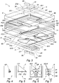
Figure 3 est une vue schématique en perspective éclatée et en transparence d'une cellule élémentaire selon l'invention. -
Figure 4 est une vue schématique partielle, de dessus, d'une cellule élémentaire selon l'invention, illustrant la première surface du deuxième substrat diélectrique munie d'un plan de masse. -
Figure 5 est une vue schématique partielle, de dessus, d'une cellule élémentaire selon l'invention, illustrant la seconde surface du deuxième substrat diélectrique munie de lignes quart d'onde. -
Figure 6 est une vue schématique partielle, de dessus, d'une cellule élémentaire selon l'invention, illustrant la seconde surface du premier substrat diélectrique munie de lignes de polarisation des commutateurs. -
Figure 7 est une vue schématique partielle, de dessus, d'une cellule élémentaire selon l'invention, illustrant la première surface du premier substrat diélectrique munie d'une antenne de réception.
-
Figure 1 is a schematic view of a reconfigurable antenna with a transmitter network. -
Figure 2 is a schematic sectional view of an elementary cell according to the invention. -
Figure 3 is a schematic perspective exploded and transparent view of an elementary cell according to the invention. -
Figure 4 is a partial schematic view, from above, of an elementary cell according to the invention, illustrating the first surface of the second dielectric substrate provided with a ground plane. -
Figure 5 is a partial schematic view, from above, of an elementary cell according to the invention, illustrating the second surface of the second dielectric substrate provided with quarter-wave lines. -
Figure 6 is a partial schematic view, from above, of an elementary cell according to the invention, illustrating the second surface of the first dielectric substrate provided with polarization lines of the switches. -
Figure 7 is a partial schematic view, from above, of an elementary cell according to the invention, illustrating the first surface of the first dielectric substrate provided with a receiving antenna.
Les éléments identiques ou assurant la même fonction porteront les mêmes références pour les différents modes de réalisation, par souci de simplification.The identical elements or ensuring the same function will bear the same references for the various embodiments, for the sake of simplification.
Un objet de l'invention est une cellule élémentaire 1 d'un réseau transmetteur RT pour une antenne reconfigurable à une fréquence de fonctionnement, la cellule élémentaire 1 comportant :
- une antenne de réception 2, planaire, destinée à recevoir une onde incidente Ei ;
- une antenne de
transmission 3, planaire, destinée à transmettre l'onde incidente Ei avec un déphasage (l'onde transmise Et déphasée étant illustrée à lafigure 1 ), et comprenant des première et deuxième surfaces de rayonnement 30, 31 disjointes ; - un premier circuit de déphasage 4, configuré pour définir un premier couple d'états de phase pour l'onde incidente Ei ; le premier circuit de déphasage 4 comprenant des premier et
second commutateurs transmission 3 ;
- a
planar receiving antenna 2 for receiving an incident wave E i ; - a
planar transmission antenna 3 for transmitting the incident wave E i with a phase shift (the transmitted wave E t out of phase being illustrated in FIG.figure 1 ), and comprising first and second radiating surfaces 30, 31 disjoined; - a first phase shift circuit 4, configured to define a first pair of phase states for the incident wave E i ; the first phase shift circuit 4 comprising first and
second switches radiated surfaces transmission antenna 3;
La cellule élémentaire 1 comporte avantageusement un premier substrat diélectrique 6 comprenant :
une première surface 60, munie de l'antenne de réception 2 ;une seconde surface 61, opposée à la premièresurface 60, et munie de lignes depolarisation 610 agencées pour polariser les premier etsecond commutateurs
- a
first surface 60, provided with the receivingantenna 2; - a
second surface 61, opposite to thefirst surface 60, and provided withpolarization lines 610 arranged to bias the first andsecond switches
A titre d'exemple non limitatif, le premier substrat diélectrique 6 peut présenter une épaisseur de l'ordre de 254 µm lorsque la fréquence de fonctionnement est 29 GHz. A titre d'exemple non limitatif, le premier substrat diélectrique 6 peut être réalisé dans un matériau commercial tel que le RT/duroid® 6002.By way of non-limiting example, the first
L'antenne de réception 2 est une antenne planaire («patch» en langue anglaise). Les première et deuxième surfaces de captation 20, 21 sont agencées pour capter l'onde incidente Ei. Les première et deuxième surfaces de captation 20, 21 sont disjointes au sens où elles sont séparées entre elles par une zone de séparation ZS1 de manière à être électriquement isolées entre elles. A cet effet, une fente est avantageusement ménagée dans l'antenne de réception 2 pour isoler électriquement les première et deuxième surfaces de captation 20, 21. La fente définit la zone de séparation ZS1. La fente est préférentiellement annulaire, à section rectangulaire. Bien entendu, d'autres formes sont envisageables pour la fente, telles qu'une forme elliptique ou circulaire. Selon une variante d'exécution, l'isolation électrique des première et deuxième surfaces de captation 20, 21 peut être assurée par un matériau diélectrique.The receiving
Les première et deuxième surfaces de captation 20, 21 présentent avantageusement un axe de symétrie afin de ne pas dégrader la polarisation de l'onde incidente Ei. La première surface de captation 20 forme préférentiellement un anneau à section rectangulaire. La deuxième surface de captation 21 forme préférentiellement une bande rectangulaire. La deuxième surface de captation 21 est avantageusement circonscrite par la première surface de captation 20 afin d'éviter la formation de courants parasites. Les première et deuxième surfaces de captation 20, 21 sont préférentiellement réalisées dans un matériau métallique, plus préférentiellement le cuivre. Des surfaces de captation additionnelles peuvent être avantageusement empilées sur les première et deuxième surfaces de captation 20, 21 afin d'augmenter la bande passante de l'antenne de réception 2.The first and second capture surfaces 20, 21 advantageously have an axis of symmetry so as not to degrade the polarization of the incident wave E i . The
La cellule élémentaire 1 comporte avantageusement une ligne à retard LR configurée de sorte que le second couple d'états de phase est déphasé de 90° par rapport au premier couple d'états de phase. Pour ce faire, la ligne à retard LR présente une longueur adaptée de sorte que le second couple d'états de phase est déphasé de 90° par rapport au premier couple d'états de phase. La ligne à retard LR s'étend avantageusement à partir de l'antenne de réception 2. Plus précisément, comme illustré à la
La cellule élémentaire 1 comporte avantageusement un deuxième substrat diélectrique 7 comprenant :
une première surface 70, munie d'un plan de masse PM ;une seconde surface 71, opposée à la premièresurface 70.
- a
first surface 70, provided with a ground plane PM; - a
second surface 71, opposite thefirst surface 70.
A titre d'exemple non limitatif, le deuxième substrat diélectrique 7 peut présenter une épaisseur de l'ordre de 254 µm lorsque la fréquence de fonctionnement est 29 GHz. A titre d'exemple non limitatif, le deuxième substrat diélectrique 7 peut être réalisé dans un matériau commercial tel que le RT/duroid® 6002.By way of non-limiting example, the second
Le plan de masse PM est préférentiellement réalisé dans un matériau métallique, plus préférentiellement le cuivre. A titre d'exemple non limitatif, le plan de masse PM peut présenter une épaisseur de l'ordre de 17 µm lorsque la fréquence de fonctionnement est 29 GHz.The mass plane PM is preferably made of a metallic material, more preferably copper. By way of non-limiting example, the ground plane PM may have a thickness of the order of 17 μm when the operating frequency is 29 GHz.
La seconde surface 71 du deuxième substrat diélectrique 7 est avantageusement munie de lignes quart d'onde 710 électriquement connectées au plan de masse PM par l'intermédiaire d'un trou d'interconnexion 711 traversant le deuxième substrat diélectrique 7. Les lignes quart d'onde 710 sont préférentiellement réalisées dans un matériau métallique, plus préférentiellement le cuivre.The
La cellule élémentaire 1 comporte avantageusement un troisième substrat diélectrique 8 comprenant :
une première surface 80, munie de l'antenne detransmission 3 ;une seconde surface 81, opposée à la premièresurface 80, et munie de lignes depolarisation 810 agencées pour polariser les premier etsecond commutateurs
- a
first surface 80, provided with thetransmission antenna 3; - a
second surface 81, opposite thefirst surface 80, and provided withpolarization lines 810 arranged to bias the first andsecond switches
A titre d'exemple non limitatif, le troisième substrat diélectrique 8 peut présenter une épaisseur de l'ordre de 508 µm lorsque la fréquence de fonctionnement est 29 GHz. A titre d'exemple non limitatif, le troisième substrat diélectrique 8 peut être réalisé dans un matériau commercial tel que le RT/duroid® 6002.By way of nonlimiting example, the third
L'antenne de transmission 3 est une antenne planaire (« patch » en langue anglaise). Les première et deuxième surfaces de rayonnement 30, 31 sont disjointes au sens où elles sont séparées entre elles par une zone de séparation ZS2 de manière à être électriquement isolées entre elles. A cet effet, une fente est avantageusement ménagée dans l'antenne de transmission 3 pour isoler électriquement les première et deuxième surfaces de rayonnement 30, 31. La fente définit la zone de séparation ZS2. La fente est préférentiellement annulaire, à section rectangulaire. Bien entendu, d'autres formes sont envisageables pour la fente, telles qu'une forme elliptique ou circulaire. Selon une variante d'exécution, l'isolation électrique des première et deuxième surfaces de rayonnement 30, 31 peut être assurée par un matériau diélectrique.The
Les première et deuxième surfaces de rayonnement 30, 31 présentent avantageusement un axe de symétrie afin de ne pas dégrader la polarisation de l'onde transmise Et par l'antenne de transmission 3 en minimisant l'excitation de modes de résonance non désirés. La première surface de rayonnement 30 forme préférentiellement un anneau à section rectangulaire. La deuxième surface de rayonnement 31 forme préférentiellement une bande rectangulaire. La deuxième surface de rayonnement 31 est avantageusement circonscrite par la première surface de rayonnement 30 afin d'éviter la formation de courants parasites. Les première et deuxième surfaces de rayonnement 30, 31 sont préférentiellement réalisées dans un matériau métallique, plus préférentiellement le cuivre. Des surfaces de rayonnement additionnelles peuvent être avantageusement empilées sur les première et deuxième surfaces de rayonnement 30, 31 afin d'augmenter la bande passante de l'antenne de transmission 3.The first and second radiation surfaces 30, 31 advantageously have an axis of symmetry so as not to degrade the polarization of the transmitted wave E t by the
L'antenne de réception 2 et l'antenne de transmission 3 peuvent avantageusement être orientées l'une par rapport à l'autre de manière à modifier la polarisation de l'onde incidente Ei. Ainsi, une rotation de l'antenne de transmission 3 de 90° relativement à l'antenne de réception 2 permet de passer, par exemple, d'une polarisation verticale de l'onde incidente Ei à une polarisation horizontale de l'onde transmise Et.The
Le premier circuit de déphasage 4 comporte des lignes de polarisation 810 agencées pour polariser les premier et second commutateurs 40, 41. Les lignes de polarisation 810 sont des pistes électriquement conductrices, formant des moyens de commande des premier et second commutateurs 40, 41. Les lignes de polarisation 810 sont préférentiellement réalisées dans un matériau métallique, plus préférentiellement le cuivre. Comme évoqué précédemment, les lignes de polarisation 810 du premier circuit de déphasage 4 sont avantageusement agencées à la seconde surface 81 du troisième substrat diélectrique 8. Les lignes de polarisation 810 du premier circuit de déphasage 4 sont électriquement connectées à l'antenne de transmission 3, plus précisément à la première surface de rayonnement 30 de l'antenne de transmission 3, par l'intermédiaire d'un trou d'interconnexion 811 traversant le troisième substrat diélectrique 8. Comme illustré à la
De la même façon, le deuxième circuit de déphasage 5 comporte des lignes de polarisation 610 agencées pour polariser les premier et second commutateurs 50, 51. Les lignes de polarisation 610 sont des pistes électriquement conductrices, formant des moyens de commande des premier et second commutateurs 50, 51. Les lignes de polarisation 610 sont préférentiellement réalisées dans un matériau métallique, plus préférentiellement le cuivre. Comme évoqué précédemment, les lignes de polarisation 610 du deuxième circuit de déphasage 5 sont avantageusement agencées à la seconde surface 61 du premier substrat diélectrique 6. Les lignes de polarisation 610 du deuxième circuit de déphasage 5 sont électriquement connectées à l'antenne de réception 2, plus précisément à la première surface de captation 20 de l'antenne de réception 2, par l'intermédiaire d'un trou d'interconnexion 611 traversant le premier substrat diélectrique 6. Comme illustré aux
Les premier et second commutateurs 40, 41 du premier circuit de déphasage 4 peuvent s'étendre sur les première et deuxième surfaces de rayonnement 30, 31 de l'antenne de transmission 3. A titre de variante, les premier et second commutateurs 40, 41 du premier circuit de déphasage 4 peuvent être formés à la première surface 80 du troisième substrat diélectrique 8, dans la zone de séparation ZS2 des première et deuxième surfaces de rayonnement 30, 31 de l'antenne de transmission 3. Les premier et second commutateurs 40, 41 du premier circuit de déphasage 4 sont avantageusement formés à la première surface 80 du troisième substrat diélectrique 8, dans la zone de séparation ZS2, de manière monolithique avec l'antenne de transmission 3. Par « monolithique », on entend que l'antenne de transmission 3 et les premier et second commutateurs 40, 41 du premier circuit de déphasage 4 partagent un unique substrat, en l'espèce le troisième substrat diélectrique 8. Les premier et second commutateurs 50, 51 du deuxième circuit de déphasage 5 peuvent s'étendre sur les première et deuxième surfaces de captation 20, 21 de l'antenne de réception 2. A titre de variante, les premier et second commutateurs 50, 51 du deuxième circuit de déphasage 5 peuvent être formés à la première surface 60 du premier substrat diélectrique 6, dans la zone de séparation ZS1 des première et deuxième surfaces de captation 20, 21 de l'antenne de réception 2. Les premier et second commutateurs 50, 51 du deuxième circuit de déphasage 5 sont avantageusement formés à la première surface 60 du premier substrat diélectrique 6, dans la zone de séparation ZS1, de manière monolithique avec l'antenne de réception 2. Par « monolithique », on entend que l'antenne de réception 2 et les premier et second commutateurs 50, 51 du deuxième circuit de déphasage 5 partagent un unique substrat, en l'espèce le premier substrat diélectrique 6.The first and
A titre d'exemples non limitatifs, les premier et second commutateurs 40, 41 ; 50, 51 des premier et deuxième circuits de déphasage 4, 5 peuvent être des diodes de type p-i-n, des MEMS (« Micro Electro-Mechanical Systems » en langue anglaise), des NEMS (« Nano Electro-Mechanical Systems » en langue anglaise). Les diodes de type p-i-n peuvent être réalisées en AlGaAs.By way of nonlimiting examples, the first and
D'autres formes d'exécution sont envisageables pour les commutateurs. A titre d'exemples non limitatifs, des commutateurs radiofréquence de type diodes, transistors, photodiodes, phototransistor sont possibles. Le choix d'un dispositif pour commander les commutateurs dépend de la technologie choisie. A titre d'exemples, les dispositifs suivants peuvent être utilisés :
- une fibre optique pour un commutateur de type photoélectrique,
- un faisceau laser généré par des moyens extérieurs et excitant un commutateur de type photoélectrique,
- une onde électromagnétique selon les principes de la télé-alimentation connus du domaine de la RFID (« Radio Frequency Identification » en langue anglaise).
- an optical fiber for a photoelectric type switch,
- a laser beam generated by external means and exciting a photoelectric switch,
- an electromagnetic wave according to the principles of remote power supply known from the field of RFID (" Radio Frequency Identification " in English).
Le premier commutateur 40 du premier circuit de déphasage 4 alterne entre l'état passant et l'état bloqué, tandis que, simultanément, le second commutateur 41 du premier circuit de déphasage 4 alterne entre l'état bloqué et l'état passant. En d'autres termes, à tout instant, les premier et second commutateurs 40, 41 appartenant au premier circuit de déphasage 4 présentent deux états opposés, soit passant/bloqué, soit bloqué/passant. Les états passant/passant ou bloqué/bloqué ne sont pas autorisés. De la même façon, le premier commutateur 50 du deuxième circuit de déphasage 5 alterne entre l'état passant et l'état bloqué, tandis que, simultanément, le second commutateur 51 du deuxième circuit de déphasage 5 alterne entre l'état bloqué et l'état passant. En d'autres termes, à tout instant, les premier et second commutateurs 50, 51 appartenant au deuxième circuit de déphasage 5 présentent deux états opposés, soit passant/bloqué, soit bloqué/passant. Les états passant/passant ou bloqué/bloqué ne sont pas autorisés. Comme illustré dans le tableau ci-après, il est donc possible d'obtenir quatre états de phase. L'état passant est noté « 1 » tandis que l'état bloqué est noté «0 ».
L'antenne de réception 2 et l'antenne de transmission 3 sont électriquement connectées entre elles, afin de pouvoir les alimenter et de les coupler, en partie par l'intermédiaire d'un trou d'interconnexion (« via » en langue anglaise) principal VP, de préférence central, de préférence métallique. Le trou d'interconnexion principal VP traverse une ouverture ménagée dans le plan de masse PM. Le trou d'interconnexion principal VP n'est pas en contact avec le plan de masse PM de sorte que le trou d'interconnexion principal VP est électriquement isolé du plan de masse PM. Le trou d'interconnexion principal VP est avantageusement connecté aux lignes quart d'onde 710. A titre d'exemple, pour une fréquence de fonctionnement de 29 GHz, le trou d'interconnexion principal VP présente un diamètre de l'ordre de 150 µm.The receiving
Le trou d'interconnexion principal VP est préférentiellement connecté à l'antenne de réception 2 par un premier point de connexion. Le trou d'interconnexion principal VP est préférentiellement connecté à l'antenne de transmission 3 par un second point de connexion. De manière générale, la position des premier et second points de connexion varie selon la géométrie spécifique des antennes de réception et de transmission 2, 3 de manière à exciter le mode fondamental de résonance. Dans le cas des géométries illustrées à la
Plus précisément, le trou d'interconnexion principal VP traverse les premier, deuxième, et troisième substrats diélectriques 6, 7, 8. En outre, le trou d'interconnexion principal VP relie le centre de la deuxième surface de captation 21 au centre de la deuxième surface de rayonnement 31 de l'antenne de transmission 3. Le trou d'interconnexion principal VP s'étend suivant une direction correspondant à la normale à la deuxième surface de captation 21, et à la normale à la deuxième surface de rayonnement 31.More specifically, the main via VP passes through the first, second and third
La cellule élémentaire 1 comporte avantageusement un premier film de collage FC1 agencé pour coller la seconde surface 71 du deuxième substrat diélectrique 7 sur la seconde surface 61 du premier substrat diélectrique 6. Ainsi, le premier film de collage FC1 est interposé entre les premier et deuxième substrats diélectriques 6, 7. A titre d'exemple non limitatif, le premier film de collage FC1 peut présenter une épaisseur de l'ordre de 114 µm lorsque la fréquence de fonctionnement est 29 GHz.The
La cellule élémentaire 1 comporte avantageusement un second film de collage FC2 agencé pour coller la seconde surface 81 du troisième substrat diélectrique 8 sur la première surface 70 du deuxième substrat diélectrique 7. Ainsi, le second film de collage FC2 est interposé entre les deuxième et troisième substrats diélectriques 7, 8. A titre d'exemple non limitatif, le second film de collage FC1 peut présenter une épaisseur de l'ordre de 114 µm lorsque la fréquence de fonctionnement est 29 GHz.The
A titre d'exemples non limitatifs, les premier et second films de collage FC1, FC2 peuvent être réalisés dans un matériau de type copolymère thermoplastique tel que le chlorotrifluoroéthylène (CTFE). On peut citer comme films de collage commerciaux le CuClad® 6700.As non-limiting examples, the first and second bonding films FC1, FC2 may be made of a thermoplastic copolymer type material such as chlorotrifluoroethylene (CTFE). Commercial bonding films include CuClad® 6700.
Il est à noter que le trou d'interconnexion principal VP traverse également les premier et second films de collage FC1, FC2.It should be noted that the main via VP also crosses the first and second bonding films FC1, FC2.
Comme illustré à la
Les résultats obtenus pour l'architecture décrite aux
- d'augmenter la directivité de 2,3 dBi (décibel isotrope),
- d'augmenter le gain
de - d'augmenter le SLL (« Side Lobe Level») de 5,0 dB.
- to increase the directivity of 2.3 dBi (isotropic decibel),
- to increase the gain by 2.3 dBi,
- increase the SLL (" Side Lobe Level") by 5.0 dB.
En outre, la bande de transmission est relativement large (>10%) et les pertes d'insertion sont faibles (<3 dB).In addition, the transmission band is relatively wide (> 10%) and insertion losses are low (<3 dB).
L'invention ne se limite pas aux modes de réalisation exposés. L'homme du métier est mis à même de considérer leurs combinaisons techniquement opérantes, et de leur substituer des équivalents.The invention is not limited to the exposed embodiments. Those skilled in the art are able to consider their technically operating combinations, and to substitute equivalents for them.
Claims (11)
Applications Claiming Priority (1)
| Application Number | Priority Date | Filing Date | Title |
|---|---|---|---|
| FR1753285A FR3065329B1 (en) | 2017-04-14 | 2017-04-14 | ELEMENTARY CELL OF A TRANSMITTER NETWORK FOR A RECONFIGURABLE ANTENNA |
Publications (2)
| Publication Number | Publication Date |
|---|---|
| EP3392959A1 true EP3392959A1 (en) | 2018-10-24 |
| EP3392959B1 EP3392959B1 (en) | 2020-09-02 |
Family
ID=59811399
Family Applications (1)
| Application Number | Title | Priority Date | Filing Date |
|---|---|---|---|
| EP18166901.1A Active EP3392959B1 (en) | 2017-04-14 | 2018-04-11 | Elementary cell of a transmitter network for a reconfigurable antenna |
Country Status (3)
| Country | Link |
|---|---|
| US (1) | US10680329B2 (en) |
| EP (1) | EP3392959B1 (en) |
| FR (1) | FR3065329B1 (en) |
Cited By (2)
| Publication number | Priority date | Publication date | Assignee | Title |
|---|---|---|---|---|
| EP3840116A1 (en) * | 2019-12-18 | 2021-06-23 | Commissariat à l'Energie Atomique et aux Energies Alternatives | Reconfigurable antenna with transmitter network with monolithic integration of elementary cells |
| EP4117117A1 (en) | 2021-07-07 | 2023-01-11 | Commissariat À L'Énergie Atomique Et Aux Énergies Alternatives | Antenna cell with transmitter network |
Families Citing this family (11)
| Publication number | Priority date | Publication date | Assignee | Title |
|---|---|---|---|---|
| US10171139B1 (en) | 2016-02-02 | 2019-01-01 | Ethertronics, Inc. | Inter-dwelling signal management using reconfigurable antennas |
| RU196050U1 (en) * | 2019-10-04 | 2020-02-14 | Федеральное государственное автономное образовательное учреждение высшего образования "Санкт-Петербургский государственный электротехнический университет "ЛЭТИ" им. В.И. Ульянова (Ленина) | Modular walk through antenna cell |
| FR3105612B1 (en) * | 2019-12-18 | 2023-09-15 | Commissariat Energie Atomique | Compact resonant cavity antenna |
| FR3105613B1 (en) * | 2019-12-18 | 2021-12-17 | Commissariat Energie Atomique | Elementary cell of a transmitting network |
| CN111490351B (en) * | 2020-03-18 | 2021-07-16 | 南京星腾通信技术有限公司 | Digital phased array antenna with multiple bit quantization |
| CN111585003B (en) * | 2020-05-22 | 2022-02-01 | 甬矽电子(宁波)股份有限公司 | IC packaging radio frequency structure and manufacturing method thereof |
| RU205718U1 (en) * | 2020-12-25 | 2021-07-30 | Федеральное государственное автономное образовательное учреждение высшего образования "Санкт-Петербургский государственный электротехнический университет "ЛЭТИ" им. В.И. Ульянова (Ленина) | Cell of modular loop-through antenna array |
| FR3122780A1 (en) | 2021-05-07 | 2022-11-11 | Commissariat A L'energie Atomique Et Aux Energies Alternatives | Transmitter array antenna cell |
| FR3123513A1 (en) * | 2021-06-01 | 2022-12-02 | Commissariat A L'energie Atomique Et Aux Energies Alternatives | Stack for manufacturing an integrated circuit intended to provide an electromagnetic lens function for a reconfigurable antenna with a transmitter array |
| FR3135572A1 (en) | 2022-05-11 | 2023-11-17 | Commissariat A L'energie Atomique Et Aux Energies Alternatives | LOW PROFILE ANTENNA WITH TWO-DIMENSIONAL ELECTRONIC SCANNING |
| WO2024035054A1 (en) * | 2022-08-11 | 2024-02-15 | Corning Incorporated | Devices to direct the path of electromagnetic radiation |
Citations (5)
| Publication number | Priority date | Publication date | Assignee | Title |
|---|---|---|---|---|
| FR2445036A1 (en) * | 1978-12-22 | 1980-07-18 | Thomson Csf | ELECTRONIC SCANNING MICROWAVE DEPHASER AND ANTENNA HAVING SUCH A PHASER |
| US6184828B1 (en) * | 1992-11-18 | 2001-02-06 | Kabushiki Kaisha Toshiba | Beam scanning antennas with plurality of antenna elements for scanning beam direction |
| US6556168B1 (en) * | 1998-12-24 | 2003-04-29 | Nec Corporation | Phased array antenna and its manufacturing method |
| US7030824B1 (en) * | 2003-05-29 | 2006-04-18 | Lockheed Martin Corporation | MEMS reflectarray antenna for satellite applications |
| FR2969832A1 (en) * | 2010-12-24 | 2012-06-29 | Commissariat Energie Atomique | RADIATION CELL WITH TWO PHASE STATES FOR TRANSMITTER NETWORK |
Family Cites Families (3)
| Publication number | Priority date | Publication date | Assignee | Title |
|---|---|---|---|---|
| WO2009023551A1 (en) | 2007-08-10 | 2009-02-19 | Arizona Board Of Regents And On Behalf Of Arizona State University | Hybrid integrated mems reconfigurable antenna array (himra) |
| US7791552B1 (en) * | 2007-10-12 | 2010-09-07 | The United States Of America As Represented By The Administrator Of The National Aeronautics And Space Administration | Cellular reflectarray antenna and method of making same |
| US10511100B2 (en) * | 2016-02-02 | 2019-12-17 | Georgia Tech Research Corporation | Inkjet printed flexible Van Atta array sensor |
-
2017
- 2017-04-14 FR FR1753285A patent/FR3065329B1/en not_active Expired - Fee Related
-
2018
- 2018-04-11 EP EP18166901.1A patent/EP3392959B1/en active Active
- 2018-04-12 US US15/951,680 patent/US10680329B2/en active Active
Patent Citations (5)
| Publication number | Priority date | Publication date | Assignee | Title |
|---|---|---|---|---|
| FR2445036A1 (en) * | 1978-12-22 | 1980-07-18 | Thomson Csf | ELECTRONIC SCANNING MICROWAVE DEPHASER AND ANTENNA HAVING SUCH A PHASER |
| US6184828B1 (en) * | 1992-11-18 | 2001-02-06 | Kabushiki Kaisha Toshiba | Beam scanning antennas with plurality of antenna elements for scanning beam direction |
| US6556168B1 (en) * | 1998-12-24 | 2003-04-29 | Nec Corporation | Phased array antenna and its manufacturing method |
| US7030824B1 (en) * | 2003-05-29 | 2006-04-18 | Lockheed Martin Corporation | MEMS reflectarray antenna for satellite applications |
| FR2969832A1 (en) * | 2010-12-24 | 2012-06-29 | Commissariat Energie Atomique | RADIATION CELL WITH TWO PHASE STATES FOR TRANSMITTER NETWORK |
Cited By (7)
| Publication number | Priority date | Publication date | Assignee | Title |
|---|---|---|---|---|
| EP3840116A1 (en) * | 2019-12-18 | 2021-06-23 | Commissariat à l'Energie Atomique et aux Energies Alternatives | Reconfigurable antenna with transmitter network with monolithic integration of elementary cells |
| FR3105610A1 (en) * | 2019-12-18 | 2021-06-25 | Commissariat A L'energie Atomique Et Aux Energies Alternatives | Reconfigurable antenna with transmitter network with monolithic integration of elementary cells |
| US11296423B2 (en) | 2019-12-18 | 2022-04-05 | Commissariat A L'energie Atomique Et Aux Energies Alternatives | Reconfigurable transmitarray antenna with monolithic integration of elementary cells |
| EP4117117A1 (en) | 2021-07-07 | 2023-01-11 | Commissariat À L'Énergie Atomique Et Aux Énergies Alternatives | Antenna cell with transmitter network |
| US20230010547A1 (en) * | 2021-07-07 | 2023-01-12 | Commissariat A L'energie Atomique Et Aux Energies Alternatives | Transmitarray antenna cell |
| FR3125173A1 (en) | 2021-07-07 | 2023-01-13 | Commissariat A L'energie Atomique Et Aux Energies Alternatives | Transmitter array antenna cell |
| US11962094B2 (en) | 2021-07-07 | 2024-04-16 | Commissariat à l'Energie Atomique et aux Energies Alternatives | Transmitarray antenna cell |
Also Published As
| Publication number | Publication date |
|---|---|
| FR3065329A1 (en) | 2018-10-19 |
| FR3065329B1 (en) | 2019-07-05 |
| US10680329B2 (en) | 2020-06-09 |
| EP3392959B1 (en) | 2020-09-02 |
| US20180301807A1 (en) | 2018-10-18 |
Similar Documents
| Publication | Publication Date | Title |
|---|---|---|
| EP3392959B1 (en) | Elementary cell of a transmitter network for a reconfigurable antenna | |
| EP3125362B1 (en) | Elementary cell of a transmitter network for a reconfigurable antenna | |
| EP2532046B1 (en) | Flat-plate scanning antenna for land mobile application, vehicle comprising such an antenna, and satellite telecommunication system comprising such a vehicle | |
| EP2656438B1 (en) | Radio cell with two phase states for transmit array | |
| EP0064313B1 (en) | Circularly polarised microwave radiating element and flat microwave antenna using an array of such elements | |
| EP1580844B1 (en) | Phase shifter with linear polarization and a resonating length which can be varied using mem switches. | |
| EP2532050B1 (en) | On-board directional flat-plate antenna, vehicle comprising such an antenna, and satellite telecommunication system comprising such a vehicle | |
| EP0497702B1 (en) | Radiating element structure for a plate antenna | |
| FR2648626A1 (en) | RADIANT ELEMENT DIPLEXANT | |
| EP2673842B1 (en) | Waveguide antenna having annular slots | |
| EP3840122A1 (en) | Elementary cell of a transmitter array | |
| EP3840116B1 (en) | Reconfigurable antenna with transmitter network with monolithic integration of elementary cells | |
| EP3840115A1 (en) | Antenna with compact resonant cavity | |
| EP4117117A1 (en) | Antenna cell with transmitter network | |
| CA2808511C (en) | Flat antenna for a terminal operating in dual circular polarisation, airborne terminal and satellite telecommunication system featuring at least one antenna | |
| FR2724491A1 (en) | MINIATURIZED, DOUBLE-POLARIZED, VERY WIDE BAND PLATED ANTENNA | |
| EP4099498A1 (en) | Stack for manufacturing an integrated circuit intended for providing an electromagnetic lens function for a reconfigurable antenna with transmitter network | |
| EP2190061A1 (en) | Radiating element network and antenna comprising such a network | |
| WO2023218008A1 (en) | Low-profile antenna with two-dimensional electronic scanning | |
| FR3085550A1 (en) | COMPACT ANTENNAIRE DEVICE | |
| EP2889955A1 (en) | Compact antenna structure for satellite telecommunication |
Legal Events
| Date | Code | Title | Description |
|---|---|---|---|
| PUAI | Public reference made under article 153(3) epc to a published international application that has entered the european phase |
Free format text: ORIGINAL CODE: 0009012 |
|
| STAA | Information on the status of an ep patent application or granted ep patent |
Free format text: STATUS: REQUEST FOR EXAMINATION WAS MADE |
|
| 17P | Request for examination filed |
Effective date: 20180411 |
|
| AK | Designated contracting states |
Kind code of ref document: A1 Designated state(s): AL AT BE BG CH CY CZ DE DK EE ES FI FR GB GR HR HU IE IS IT LI LT LU LV MC MK MT NL NO PL PT RO RS SE SI SK SM TR |
|
| AX | Request for extension of the european patent |
Extension state: BA ME |
|
| STAA | Information on the status of an ep patent application or granted ep patent |
Free format text: STATUS: EXAMINATION IS IN PROGRESS |
|
| 17Q | First examination report despatched |
Effective date: 20190516 |
|
| REG | Reference to a national code |
Ref country code: DE Ref legal event code: R079 Ref document number: 602018007364 Country of ref document: DE Free format text: PREVIOUS MAIN CLASS: H01Q0001220000 Ipc: H01Q0003460000 |
|
| GRAP | Despatch of communication of intention to grant a patent |
Free format text: ORIGINAL CODE: EPIDOSNIGR1 |
|
| STAA | Information on the status of an ep patent application or granted ep patent |
Free format text: STATUS: GRANT OF PATENT IS INTENDED |
|
| RIC1 | Information provided on ipc code assigned before grant |
Ipc: H01Q 3/34 20060101ALI20200320BHEP Ipc: H01Q 21/00 20060101ALI20200320BHEP Ipc: H01Q 1/22 20060101ALI20200320BHEP Ipc: H01Q 3/46 20060101AFI20200320BHEP Ipc: H01Q 9/04 20060101ALI20200320BHEP |
|
| INTG | Intention to grant announced |
Effective date: 20200414 |
|
| GRAS | Grant fee paid |
Free format text: ORIGINAL CODE: EPIDOSNIGR3 |
|
| GRAA | (expected) grant |
Free format text: ORIGINAL CODE: 0009210 |
|
| STAA | Information on the status of an ep patent application or granted ep patent |
Free format text: STATUS: THE PATENT HAS BEEN GRANTED |
|
| AK | Designated contracting states |
Kind code of ref document: B1 Designated state(s): AL AT BE BG CH CY CZ DE DK EE ES FI FR GB GR HR HU IE IS IT LI LT LU LV MC MK MT NL NO PL PT RO RS SE SI SK SM TR |
|
| REG | Reference to a national code |
Ref country code: GB Ref legal event code: FG4D Free format text: NOT ENGLISH |
|
| REG | Reference to a national code |
Ref country code: AT Ref legal event code: REF Ref document number: 1309876 Country of ref document: AT Kind code of ref document: T Effective date: 20200915 Ref country code: CH Ref legal event code: EP |
|
| REG | Reference to a national code |
Ref country code: DE Ref legal event code: R096 Ref document number: 602018007364 Country of ref document: DE |
|
| REG | Reference to a national code |
Ref country code: IE Ref legal event code: FG4D Free format text: LANGUAGE OF EP DOCUMENT: FRENCH |
|
| REG | Reference to a national code |
Ref country code: LT Ref legal event code: MG4D |
|
| PG25 | Lapsed in a contracting state [announced via postgrant information from national office to epo] |
Ref country code: FI Free format text: LAPSE BECAUSE OF FAILURE TO SUBMIT A TRANSLATION OF THE DESCRIPTION OR TO PAY THE FEE WITHIN THE PRESCRIBED TIME-LIMIT Effective date: 20200902 Ref country code: LT Free format text: LAPSE BECAUSE OF FAILURE TO SUBMIT A TRANSLATION OF THE DESCRIPTION OR TO PAY THE FEE WITHIN THE PRESCRIBED TIME-LIMIT Effective date: 20200902 Ref country code: BG Free format text: LAPSE BECAUSE OF FAILURE TO SUBMIT A TRANSLATION OF THE DESCRIPTION OR TO PAY THE FEE WITHIN THE PRESCRIBED TIME-LIMIT Effective date: 20201202 Ref country code: NO Free format text: LAPSE BECAUSE OF FAILURE TO SUBMIT A TRANSLATION OF THE DESCRIPTION OR TO PAY THE FEE WITHIN THE PRESCRIBED TIME-LIMIT Effective date: 20201202 Ref country code: GR Free format text: LAPSE BECAUSE OF FAILURE TO SUBMIT A TRANSLATION OF THE DESCRIPTION OR TO PAY THE FEE WITHIN THE PRESCRIBED TIME-LIMIT Effective date: 20201203 Ref country code: HR Free format text: LAPSE BECAUSE OF FAILURE TO SUBMIT A TRANSLATION OF THE DESCRIPTION OR TO PAY THE FEE WITHIN THE PRESCRIBED TIME-LIMIT Effective date: 20200902 Ref country code: SE Free format text: LAPSE BECAUSE OF FAILURE TO SUBMIT A TRANSLATION OF THE DESCRIPTION OR TO PAY THE FEE WITHIN THE PRESCRIBED TIME-LIMIT Effective date: 20200902 |
|
| REG | Reference to a national code |
Ref country code: NL Ref legal event code: MP Effective date: 20200902 |
|
| REG | Reference to a national code |
Ref country code: AT Ref legal event code: MK05 Ref document number: 1309876 Country of ref document: AT Kind code of ref document: T Effective date: 20200902 |
|
| PG25 | Lapsed in a contracting state [announced via postgrant information from national office to epo] |
Ref country code: PL Free format text: LAPSE BECAUSE OF FAILURE TO SUBMIT A TRANSLATION OF THE DESCRIPTION OR TO PAY THE FEE WITHIN THE PRESCRIBED TIME-LIMIT Effective date: 20200902 Ref country code: LV Free format text: LAPSE BECAUSE OF FAILURE TO SUBMIT A TRANSLATION OF THE DESCRIPTION OR TO PAY THE FEE WITHIN THE PRESCRIBED TIME-LIMIT Effective date: 20200902 Ref country code: RS Free format text: LAPSE BECAUSE OF FAILURE TO SUBMIT A TRANSLATION OF THE DESCRIPTION OR TO PAY THE FEE WITHIN THE PRESCRIBED TIME-LIMIT Effective date: 20200902 |
|
| PG25 | Lapsed in a contracting state [announced via postgrant information from national office to epo] |
Ref country code: SM Free format text: LAPSE BECAUSE OF FAILURE TO SUBMIT A TRANSLATION OF THE DESCRIPTION OR TO PAY THE FEE WITHIN THE PRESCRIBED TIME-LIMIT Effective date: 20200902 Ref country code: CZ Free format text: LAPSE BECAUSE OF FAILURE TO SUBMIT A TRANSLATION OF THE DESCRIPTION OR TO PAY THE FEE WITHIN THE PRESCRIBED TIME-LIMIT Effective date: 20200902 Ref country code: RO Free format text: LAPSE BECAUSE OF FAILURE TO SUBMIT A TRANSLATION OF THE DESCRIPTION OR TO PAY THE FEE WITHIN THE PRESCRIBED TIME-LIMIT Effective date: 20200902 Ref country code: PT Free format text: LAPSE BECAUSE OF FAILURE TO SUBMIT A TRANSLATION OF THE DESCRIPTION OR TO PAY THE FEE WITHIN THE PRESCRIBED TIME-LIMIT Effective date: 20210104 Ref country code: EE Free format text: LAPSE BECAUSE OF FAILURE TO SUBMIT A TRANSLATION OF THE DESCRIPTION OR TO PAY THE FEE WITHIN THE PRESCRIBED TIME-LIMIT Effective date: 20200902 |
|
| PG25 | Lapsed in a contracting state [announced via postgrant information from national office to epo] |
Ref country code: AL Free format text: LAPSE BECAUSE OF FAILURE TO SUBMIT A TRANSLATION OF THE DESCRIPTION OR TO PAY THE FEE WITHIN THE PRESCRIBED TIME-LIMIT Effective date: 20200902 Ref country code: AT Free format text: LAPSE BECAUSE OF FAILURE TO SUBMIT A TRANSLATION OF THE DESCRIPTION OR TO PAY THE FEE WITHIN THE PRESCRIBED TIME-LIMIT Effective date: 20200902 Ref country code: ES Free format text: LAPSE BECAUSE OF FAILURE TO SUBMIT A TRANSLATION OF THE DESCRIPTION OR TO PAY THE FEE WITHIN THE PRESCRIBED TIME-LIMIT Effective date: 20200902 Ref country code: IS Free format text: LAPSE BECAUSE OF FAILURE TO SUBMIT A TRANSLATION OF THE DESCRIPTION OR TO PAY THE FEE WITHIN THE PRESCRIBED TIME-LIMIT Effective date: 20210102 |
|
| REG | Reference to a national code |
Ref country code: DE Ref legal event code: R097 Ref document number: 602018007364 Country of ref document: DE |
|
| PG25 | Lapsed in a contracting state [announced via postgrant information from national office to epo] |
Ref country code: SK Free format text: LAPSE BECAUSE OF FAILURE TO SUBMIT A TRANSLATION OF THE DESCRIPTION OR TO PAY THE FEE WITHIN THE PRESCRIBED TIME-LIMIT Effective date: 20200902 |
|
| PLBE | No opposition filed within time limit |
Free format text: ORIGINAL CODE: 0009261 |
|
| STAA | Information on the status of an ep patent application or granted ep patent |
Free format text: STATUS: NO OPPOSITION FILED WITHIN TIME LIMIT |
|
| 26N | No opposition filed |
Effective date: 20210603 |
|
| PG25 | Lapsed in a contracting state [announced via postgrant information from national office to epo] |
Ref country code: DK Free format text: LAPSE BECAUSE OF FAILURE TO SUBMIT A TRANSLATION OF THE DESCRIPTION OR TO PAY THE FEE WITHIN THE PRESCRIBED TIME-LIMIT Effective date: 20200902 Ref country code: SI Free format text: LAPSE BECAUSE OF FAILURE TO SUBMIT A TRANSLATION OF THE DESCRIPTION OR TO PAY THE FEE WITHIN THE PRESCRIBED TIME-LIMIT Effective date: 20200902 |
|
| PG25 | Lapsed in a contracting state [announced via postgrant information from national office to epo] |
Ref country code: IT Free format text: LAPSE BECAUSE OF FAILURE TO SUBMIT A TRANSLATION OF THE DESCRIPTION OR TO PAY THE FEE WITHIN THE PRESCRIBED TIME-LIMIT Effective date: 20200902 |
|
| PG25 | Lapsed in a contracting state [announced via postgrant information from national office to epo] |
Ref country code: MC Free format text: LAPSE BECAUSE OF FAILURE TO SUBMIT A TRANSLATION OF THE DESCRIPTION OR TO PAY THE FEE WITHIN THE PRESCRIBED TIME-LIMIT Effective date: 20200902 |
|
| PG25 | Lapsed in a contracting state [announced via postgrant information from national office to epo] |
Ref country code: LU Free format text: LAPSE BECAUSE OF NON-PAYMENT OF DUE FEES Effective date: 20210411 |
|
| REG | Reference to a national code |
Ref country code: BE Ref legal event code: MM Effective date: 20210430 |
|
| PG25 | Lapsed in a contracting state [announced via postgrant information from national office to epo] |
Ref country code: CH Free format text: LAPSE BECAUSE OF NON-PAYMENT OF DUE FEES Effective date: 20210430 Ref country code: LI Free format text: LAPSE BECAUSE OF NON-PAYMENT OF DUE FEES Effective date: 20210430 |
|
| PG25 | Lapsed in a contracting state [announced via postgrant information from national office to epo] |
Ref country code: IE Free format text: LAPSE BECAUSE OF NON-PAYMENT OF DUE FEES Effective date: 20210411 |
|
| PG25 | Lapsed in a contracting state [announced via postgrant information from national office to epo] |
Ref country code: IS Free format text: LAPSE BECAUSE OF FAILURE TO SUBMIT A TRANSLATION OF THE DESCRIPTION OR TO PAY THE FEE WITHIN THE PRESCRIBED TIME-LIMIT Effective date: 20210102 |
|
| PG25 | Lapsed in a contracting state [announced via postgrant information from national office to epo] |
Ref country code: BE Free format text: LAPSE BECAUSE OF NON-PAYMENT OF DUE FEES Effective date: 20210430 |
|
| PG25 | Lapsed in a contracting state [announced via postgrant information from national office to epo] |
Ref country code: NL Free format text: LAPSE BECAUSE OF NON-PAYMENT OF DUE FEES Effective date: 20200923 Ref country code: CY Free format text: LAPSE BECAUSE OF FAILURE TO SUBMIT A TRANSLATION OF THE DESCRIPTION OR TO PAY THE FEE WITHIN THE PRESCRIBED TIME-LIMIT Effective date: 20200902 |
|
| PG25 | Lapsed in a contracting state [announced via postgrant information from national office to epo] |
Ref country code: HU Free format text: LAPSE BECAUSE OF FAILURE TO SUBMIT A TRANSLATION OF THE DESCRIPTION OR TO PAY THE FEE WITHIN THE PRESCRIBED TIME-LIMIT; INVALID AB INITIO Effective date: 20180411 |
|
| PGFP | Annual fee paid to national office [announced via postgrant information from national office to epo] |
Ref country code: FR Payment date: 20230424 Year of fee payment: 6 Ref country code: DE Payment date: 20230418 Year of fee payment: 6 |
|
| PGFP | Annual fee paid to national office [announced via postgrant information from national office to epo] |
Ref country code: GB Payment date: 20230421 Year of fee payment: 6 |