EP4099088A1 - Lichtemittierendes substrat und ansteuerverfahren dafür, lichtemittierendes modul und anzeigevorrichtung - Google Patents
Lichtemittierendes substrat und ansteuerverfahren dafür, lichtemittierendes modul und anzeigevorrichtung Download PDFInfo
- Publication number
- EP4099088A1 EP4099088A1 EP20922728.9A EP20922728A EP4099088A1 EP 4099088 A1 EP4099088 A1 EP 4099088A1 EP 20922728 A EP20922728 A EP 20922728A EP 4099088 A1 EP4099088 A1 EP 4099088A1
- Authority
- EP
- European Patent Office
- Prior art keywords
- light
- emitting
- power supply
- supply voltage
- coupled
- Prior art date
- Legal status (The legal status is an assumption and is not a legal conclusion. Google has not performed a legal analysis and makes no representation as to the accuracy of the status listed.)
- Granted
Links
Images


Classifications
-
- G—PHYSICS
- G09—EDUCATION; CRYPTOGRAPHY; DISPLAY; ADVERTISING; SEALS
- G09G—ARRANGEMENTS OR CIRCUITS FOR CONTROL OF INDICATING DEVICES USING STATIC MEANS TO PRESENT VARIABLE INFORMATION
- G09G3/00—Control arrangements or circuits, of interest only in connection with visual indicators other than cathode-ray tubes
- G09G3/20—Control arrangements or circuits, of interest only in connection with visual indicators other than cathode-ray tubes for presentation of an assembly of a number of characters, e.g. a page, by composing the assembly by combination of individual elements arranged in a matrix no fixed position being assigned to or needed to be assigned to the individual characters or partial characters
- G09G3/22—Control arrangements or circuits, of interest only in connection with visual indicators other than cathode-ray tubes for presentation of an assembly of a number of characters, e.g. a page, by composing the assembly by combination of individual elements arranged in a matrix no fixed position being assigned to or needed to be assigned to the individual characters or partial characters using controlled light sources
- G09G3/30—Control arrangements or circuits, of interest only in connection with visual indicators other than cathode-ray tubes for presentation of an assembly of a number of characters, e.g. a page, by composing the assembly by combination of individual elements arranged in a matrix no fixed position being assigned to or needed to be assigned to the individual characters or partial characters using controlled light sources using electroluminescent panels
- G09G3/32—Control arrangements or circuits, of interest only in connection with visual indicators other than cathode-ray tubes for presentation of an assembly of a number of characters, e.g. a page, by composing the assembly by combination of individual elements arranged in a matrix no fixed position being assigned to or needed to be assigned to the individual characters or partial characters using controlled light sources using electroluminescent panels semiconductive, e.g. using light-emitting diodes [LED]
-
- G—PHYSICS
- G09—EDUCATION; CRYPTOGRAPHY; DISPLAY; ADVERTISING; SEALS
- G09G—ARRANGEMENTS OR CIRCUITS FOR CONTROL OF INDICATING DEVICES USING STATIC MEANS TO PRESENT VARIABLE INFORMATION
- G09G3/00—Control arrangements or circuits, of interest only in connection with visual indicators other than cathode-ray tubes
- G09G3/20—Control arrangements or circuits, of interest only in connection with visual indicators other than cathode-ray tubes for presentation of an assembly of a number of characters, e.g. a page, by composing the assembly by combination of individual elements arranged in a matrix no fixed position being assigned to or needed to be assigned to the individual characters or partial characters
- G09G3/34—Control arrangements or circuits, of interest only in connection with visual indicators other than cathode-ray tubes for presentation of an assembly of a number of characters, e.g. a page, by composing the assembly by combination of individual elements arranged in a matrix no fixed position being assigned to or needed to be assigned to the individual characters or partial characters by control of light from an independent source
- G09G3/3406—Control of illumination source
- G09G3/342—Control of illumination source using several illumination sources separately controlled corresponding to different display panel areas, e.g. along one dimension such as lines
- G09G3/3426—Control of illumination source using several illumination sources separately controlled corresponding to different display panel areas, e.g. along one dimension such as lines the different display panel areas being distributed in two dimensions, e.g. matrix
-
- H—ELECTRICITY
- H05—ELECTRIC TECHNIQUES NOT OTHERWISE PROVIDED FOR
- H05B—ELECTRIC HEATING; ELECTRIC LIGHT SOURCES NOT OTHERWISE PROVIDED FOR; CIRCUIT ARRANGEMENTS FOR ELECTRIC LIGHT SOURCES, IN GENERAL
- H05B45/00—Circuit arrangements for operating light-emitting diodes [LED]
- H05B45/10—Controlling the intensity of the light
-
- H—ELECTRICITY
- H05—ELECTRIC TECHNIQUES NOT OTHERWISE PROVIDED FOR
- H05B—ELECTRIC HEATING; ELECTRIC LIGHT SOURCES NOT OTHERWISE PROVIDED FOR; CIRCUIT ARRANGEMENTS FOR ELECTRIC LIGHT SOURCES, IN GENERAL
- H05B33/00—Electroluminescent light sources
- H05B33/12—Light sources with substantially two-dimensional [2D] radiating surfaces
- H05B33/26—Light sources with substantially two-dimensional [2D] radiating surfaces characterised by the composition or arrangement of the conductive material used as an electrode
-
- H—ELECTRICITY
- H05—ELECTRIC TECHNIQUES NOT OTHERWISE PROVIDED FOR
- H05B—ELECTRIC HEATING; ELECTRIC LIGHT SOURCES NOT OTHERWISE PROVIDED FOR; CIRCUIT ARRANGEMENTS FOR ELECTRIC LIGHT SOURCES, IN GENERAL
- H05B47/00—Circuit arrangements for operating light sources in general, i.e. where the type of light source is not relevant
- H05B47/10—Controlling the light source
- H05B47/16—Controlling the light source by timing means
-
- H—ELECTRICITY
- H10—SEMICONDUCTOR DEVICES; ELECTRIC SOLID-STATE DEVICES NOT OTHERWISE PROVIDED FOR
- H10D—INORGANIC ELECTRIC SEMICONDUCTOR DEVICES
- H10D86/00—Integrated devices formed in or on insulating or conducting substrates, e.g. formed in silicon-on-insulator [SOI] substrates or on stainless steel or glass substrates
- H10D86/40—Integrated devices formed in or on insulating or conducting substrates, e.g. formed in silicon-on-insulator [SOI] substrates or on stainless steel or glass substrates characterised by multiple TFTs
- H10D86/441—Interconnections, e.g. scanning lines
-
- G—PHYSICS
- G02—OPTICS
- G02F—OPTICAL DEVICES OR ARRANGEMENTS FOR THE CONTROL OF LIGHT BY MODIFICATION OF THE OPTICAL PROPERTIES OF THE MEDIA OF THE ELEMENTS INVOLVED THEREIN; NON-LINEAR OPTICS; FREQUENCY-CHANGING OF LIGHT; OPTICAL LOGIC ELEMENTS; OPTICAL ANALOGUE/DIGITAL CONVERTERS
- G02F1/00—Devices or arrangements for the control of the intensity, colour, phase, polarisation or direction of light arriving from an independent light source, e.g. switching, gating or modulating; Non-linear optics
- G02F1/01—Devices or arrangements for the control of the intensity, colour, phase, polarisation or direction of light arriving from an independent light source, e.g. switching, gating or modulating; Non-linear optics for the control of the intensity, phase, polarisation or colour
- G02F1/13—Devices or arrangements for the control of the intensity, colour, phase, polarisation or direction of light arriving from an independent light source, e.g. switching, gating or modulating; Non-linear optics for the control of the intensity, phase, polarisation or colour based on liquid crystals, e.g. single liquid crystal display cells
- G02F1/133—Constructional arrangements; Operation of liquid crystal cells; Circuit arrangements
- G02F1/1333—Constructional arrangements; Manufacturing methods
- G02F1/1335—Structural association of cells with optical devices, e.g. polarisers or reflectors
- G02F1/1336—Illuminating devices
- G02F1/133602—Direct backlight
- G02F1/133603—Direct backlight with LEDs
-
- G—PHYSICS
- G02—OPTICS
- G02F—OPTICAL DEVICES OR ARRANGEMENTS FOR THE CONTROL OF LIGHT BY MODIFICATION OF THE OPTICAL PROPERTIES OF THE MEDIA OF THE ELEMENTS INVOLVED THEREIN; NON-LINEAR OPTICS; FREQUENCY-CHANGING OF LIGHT; OPTICAL LOGIC ELEMENTS; OPTICAL ANALOGUE/DIGITAL CONVERTERS
- G02F1/00—Devices or arrangements for the control of the intensity, colour, phase, polarisation or direction of light arriving from an independent light source, e.g. switching, gating or modulating; Non-linear optics
- G02F1/01—Devices or arrangements for the control of the intensity, colour, phase, polarisation or direction of light arriving from an independent light source, e.g. switching, gating or modulating; Non-linear optics for the control of the intensity, phase, polarisation or colour
- G02F1/13—Devices or arrangements for the control of the intensity, colour, phase, polarisation or direction of light arriving from an independent light source, e.g. switching, gating or modulating; Non-linear optics for the control of the intensity, phase, polarisation or colour based on liquid crystals, e.g. single liquid crystal display cells
- G02F1/133—Constructional arrangements; Operation of liquid crystal cells; Circuit arrangements
- G02F1/1333—Constructional arrangements; Manufacturing methods
- G02F1/1335—Structural association of cells with optical devices, e.g. polarisers or reflectors
- G02F1/1336—Illuminating devices
- G02F1/133602—Direct backlight
- G02F1/133612—Electrical details
-
- G—PHYSICS
- G09—EDUCATION; CRYPTOGRAPHY; DISPLAY; ADVERTISING; SEALS
- G09G—ARRANGEMENTS OR CIRCUITS FOR CONTROL OF INDICATING DEVICES USING STATIC MEANS TO PRESENT VARIABLE INFORMATION
- G09G2300/00—Aspects of the constitution of display devices
- G09G2300/02—Composition of display devices
- G09G2300/026—Video wall, i.e. juxtaposition of a plurality of screens to create a display screen of bigger dimensions
-
- G—PHYSICS
- G09—EDUCATION; CRYPTOGRAPHY; DISPLAY; ADVERTISING; SEALS
- G09G—ARRANGEMENTS OR CIRCUITS FOR CONTROL OF INDICATING DEVICES USING STATIC MEANS TO PRESENT VARIABLE INFORMATION
- G09G2320/00—Control of display operating conditions
- G09G2320/06—Adjustment of display parameters
- G09G2320/0626—Adjustment of display parameters for control of overall brightness
- G09G2320/0633—Adjustment of display parameters for control of overall brightness by amplitude modulation of the brightness of the illumination source
-
- G—PHYSICS
- G09—EDUCATION; CRYPTOGRAPHY; DISPLAY; ADVERTISING; SEALS
- G09G—ARRANGEMENTS OR CIRCUITS FOR CONTROL OF INDICATING DEVICES USING STATIC MEANS TO PRESENT VARIABLE INFORMATION
- G09G2320/00—Control of display operating conditions
- G09G2320/06—Adjustment of display parameters
- G09G2320/0626—Adjustment of display parameters for control of overall brightness
- G09G2320/064—Adjustment of display parameters for control of overall brightness by time modulation of the brightness of the illumination source
-
- G—PHYSICS
- G09—EDUCATION; CRYPTOGRAPHY; DISPLAY; ADVERTISING; SEALS
- G09G—ARRANGEMENTS OR CIRCUITS FOR CONTROL OF INDICATING DEVICES USING STATIC MEANS TO PRESENT VARIABLE INFORMATION
- G09G2370/00—Aspects of data communication
- G09G2370/08—Details of image data interface between the display device controller and the data line driver circuit
-
- H—ELECTRICITY
- H10—SEMICONDUCTOR DEVICES; ELECTRIC SOLID-STATE DEVICES NOT OTHERWISE PROVIDED FOR
- H10K—ORGANIC ELECTRIC SOLID-STATE DEVICES
- H10K59/00—Integrated devices, or assemblies of multiple devices, comprising at least one organic light-emitting element covered by group H10K50/00
- H10K59/10—OLED displays
- H10K59/12—Active-matrix OLED [AMOLED] displays
- H10K59/131—Interconnections, e.g. wiring lines or terminals
-
- H—ELECTRICITY
- H10—SEMICONDUCTOR DEVICES; ELECTRIC SOLID-STATE DEVICES NOT OTHERWISE PROVIDED FOR
- H10W—GENERIC PACKAGES, INTERCONNECTIONS, CONNECTORS OR OTHER CONSTRUCTIONAL DETAILS OF DEVICES COVERED BY CLASS H10
- H10W90/00—Package configurations
-
- Y—GENERAL TAGGING OF NEW TECHNOLOGICAL DEVELOPMENTS; GENERAL TAGGING OF CROSS-SECTIONAL TECHNOLOGIES SPANNING OVER SEVERAL SECTIONS OF THE IPC; TECHNICAL SUBJECTS COVERED BY FORMER USPC CROSS-REFERENCE ART COLLECTIONS [XRACs] AND DIGESTS
- Y02—TECHNOLOGIES OR APPLICATIONS FOR MITIGATION OR ADAPTATION AGAINST CLIMATE CHANGE
- Y02B—CLIMATE CHANGE MITIGATION TECHNOLOGIES RELATED TO BUILDINGS, e.g. HOUSING, HOUSE APPLIANCES OR RELATED END-USER APPLICATIONS
- Y02B20/00—Energy efficient lighting technologies, e.g. halogen lamps or gas discharge lamps
- Y02B20/40—Control techniques providing energy savings, e.g. smart controller or presence detection
Definitions
- the present disclosure relates to the field of display technologies, and in particularly, to a light-emitting substrate and a driving method therefor, a light-emitting module, and a display apparatus.
- an application of a high-dynamic range (HDR) image technology in a display apparatus can improve image quality of display images, but put forward higher requirements on color gamut and brightness of the display apparatus as well.
- the mini light-emitting diode (mini LED) has small size and high brightness, and may be widely applied to a backlight module of the display apparatus. Moreover, it may finely adjust the backlight, so as to realize a display of images with a high dynamic range.
- a light-emitting substrate in an aspect, includes a base, a plurality of light-emitting components, a plurality of first power supply voltage signal lines, and a plurality of first control circuits.
- the plurality of light-emitting components are disposed on the base, and a light-emitting components is located within a light-emitting area.
- the plurality of first power supply voltage signal lines are disposed on the base and arranged at intervals.
- the plurality of first control circuits are disposed on the base, each first control circuit is coupled to a first electrode of a light-emitting component, and each first power supply voltage signal line is coupled to at least two first control circuits.
- the first control circuit is configured to transmit a first power supply voltage signal from the first power supply voltage signal line to the first electrode of the light-emitting component coupled to the first control circuit, so as to control an amplitude of a current flowing through the light-emitting component.
- the plurality of light-emitting areas are arranged in an array, and the plurality of first control circuits are arranged in an array.
- the light-emitting components in a same row of light-emitting areas are coupled to a first power supply voltage signal line through a row of first control circuits, or light-emitting components in a same column of light-emitting areas are coupled to a first power supply voltage signal line through a column of first control circuits.
- the first control circuit is configured to receive a first light-emission signal and a first enable signal, and transmit the first power supply voltage signal to the first electrode of the light-emitting component coupled to the first control circuit according to the first light-emission signal and the first enable signal, so as to control the amplitude of the current flowing through the light-emitting component.
- the first control circuit includes: a processor, an analog-to-digital converter, and a first output sub-circuit.
- the processor is configured to receive the first light-emission signal, convert a format of the first light-emission signal, and generate a second light-emission signal.
- the analog-to-digital converter is configured to receive the first enable signal and generate a reference signal.
- the first output sub-circuit is coupled to the processor, the analog-to-digital converter, the first power supply voltage signal line, and the first electrode of the light-emitting component.
- the first output sub-circuit is configured to transmit the first power supply voltage signal from the first power supply voltage signal line to the first electrode of the light-emitting component according to the second light-emission signal from the processor and the reference signal from the analog-to-digital converter.
- the first output sub-circuit includes: a first transistor, a first resistor, a comparator, and a second transistor.
- a control electrode of the first transistor is coupled to the processor, and a second electrode of the first transistor is coupled to the first electrode of the light-emitting component.
- a first end of the first resistor is coupled to the first power supply voltage signal line.
- a non-inverting input terminal of the comparator is coupled to an output terminal of the analog-to-digital converter, and an inverting input terminal of the comparator is coupled to a second end of the first resistor.
- a control electrode of the second transistor is coupled to an output terminal of the comparator, a first electrode of the second transistor is coupled to the second end of the first resistor, and a second electrode of the second transistor is coupled to a first electrode of the first transistor.
- the light-emitting substrate includes: first control chips.
- a first control chip includes the first control circuit.
- the first control chip further includes: a first interface, a second interface, a third interface, and a fourth interface.
- the first interface is coupled to the processor in the first control circuit, and the first interface is configured to receive the first light-emission signal, and transmit the first light-emission signal to the processor.
- the second interface is coupled to the analog-to-digital converter in the first control circuit, and the second interface is configured to receive the first enable signal, and transmit the first enable signal to the analog-to-digital converter.
- the third interface is coupled to the first power supply voltage signal line and the first output sub-circuit in the first control circuit, and the third interface is configured to receive the first power supply voltage signal from the first power supply voltage signal line, and transmit the first power supply voltage signal to the first output sub-circuit.
- the fourth interface is coupled to the first output sub-circuit in the first control circuit and the first electrode of the light-emitting component, and the fourth interface is configured to transmit the first power supply voltage signal passing through the first output sub-circuit to the first electrode of the light-emitting component.
- the light-emitting substrate further includes: a second control circuit disposed on the base.
- the second control circuit is coupled to the plurality of first control circuits.
- the second control circuit is configured to receive a driving signal, and transmit a first light-emission signal and a first enable signal to each first control circuit according to the driving signal.
- the second control circuit includes: a timing control sub-circuit, a data processing sub-circuit, a memory, and an amplifier sub-circuit.
- the timing control sub-circuit is configured to generate a clock signal.
- the data processing sub-circuit is coupled to the timing control sub-circuit and the plurality of first control circuits.
- the data processing sub-circuit is configured to receive the driving signal, output second enable signals according to the driving signal and the clock signal from the timing control sub-circuit, and transmit the first light-emission signals to the plurality of first control circuits.
- the memory is configured to store a timing data and a light-emission current data for a preset light-emission mode.
- the amplifier sub-circuit is coupled to the data processing sub-circuit, the memory and the plurality of first control circuits.
- the amplifier sub-circuit is configured to amplify powers of the second enable signals from the data processing sub-circuit according to the timing data and the light-emission current data for the preset light-emission mode, generate the first enable signals, and transmit the first enable signals to the plurality of first control circuits.
- the light-emitting substrate includes: a second control chip.
- the second control chip includes the second control circuit.
- the second control chip further includes: a plurality of enable signal interfaces, a plurality of light-emission signal interfaces and a driving signal interface.
- the plurality of enable signal interfaces are coupled to the amplifier sub-circuit in the second control circuit, and each enable signal interface is coupled to at least one first control circuit.
- the enable signal interface is configured to receive the first enable signal from the amplifier sub-circuit, and transmit the first enable signal to the first control circuit coupled thereto.
- the plurality of light-emission signal interfaces are coupled to the data processing sub-circuit in the second control circuit, and each light-emission signal interface is coupled to a first control circuit.
- the light-emission signal interface is configured to receive the first light-emission signal from the data processing sub-circuit, and transmit the first light-emission signal to the first control circuit coupled thereto.
- the driving signal interface is coupled to the data processing sub-circuit, and the driving signal interface is configured to receive the driving signal and transmit the driving signal to the data processing sub-circuit.
- each enable signal interface is coupled to a row or a column of first control circuits.
- the light-emitting substrate further includes a plurality of second power supply voltage signal lines disposed on the base and arranged at intervals. Second electrodes of light-emitting components in at least two light-emitting areas are coupled to a second power supply voltage signal line.
- light-emitting components in a same row or a same column of light-emitting areas are coupled to a second power supply voltage signal line.
- the first power supply voltage signal line and the second power supply voltage signal line both extend in a column direction, or both extend in a row direction.
- the second power supply voltage signal line and the first power supply voltage signal line are of a same material and are disposed in a same layer.
- the light-emitting substrate further includes an insulating layer.
- the first power supply voltage signal line and the second power supply voltage signal line are located on a side, proximate to the base, of the insulating layer, and the light-emitting component and the first control circuit are located on a side, away from the base, of the insulating layer.
- the insulating layer is provided with first vias and second vias therein, and the first control circuit is coupled to the first power supply voltage signal line through a first via; and the second electrodes of the light-emitting components are each coupled to the second power supply voltage signal line through a second via.
- the light-emitting substrate further includes the second control circuit
- the light-emitting substrate further includes: a plurality of connecting leads disposed on the side, away from the base, of the insulating layer. The plurality of connecting leads are configured to couple the first control circuits with the second control circuit.
- the light-emitting component includes: a plurality of light-emitting devices and a plurality of conductive patterns.
- the plurality of light-emitting devices are arranged in an array.
- the plurality of light-emitting devices are sequentially connected in series by the plurality of conductive patterns.
- a cathode of one of two light-emitting devices at both ends of the line is the first electrode of the light-emitting component
- an anode of another light-emitting device of the two light-emitting devices is the second electrode of the light-emitting component.
- a light-emitting module in another aspect, includes: the light-emitting substrate as described in any one of the above embodiments, a flexible circuit board and a power supply chip.
- the light-emitting substrate includes the first power supply voltage signal line and the second power supply voltage signal lines.
- the power supply chip is bonded to the light-emitting substrate through the flexible circuit board, and the power supply chip is configured to transmit the first power supply voltage signal to the first power supply voltage signal line, and transmit a second power supply voltage signal to the second power supply voltage signal line.
- a display apparatus in yet another aspect, includes: the light-emitting module in the above embodiment and a driving chip.
- the light-emitting substrate in the light-emitting module includes the plurality of first control circuits and a second control circuit.
- the driving chip is coupled to the second control circuit, and the driving chip is configured to transmit a driving signal to the second control circuit.
- the light-emitting substrate includes the plurality of first control circuits and a second control circuit.
- the method for driving the light-emitting substrate includes: receiving, by the second control circuit, a driving signal, and transmitting, by the second control circuit, a first light-emission signal and a first enable signal to each first control circuit according to the driving signal; and transmitting, by the first control circuit, the first power supply voltage signal from the first power supply voltage signal line to the first electrode of the light-emitting component coupled to the first control circuit according to the first light-emission signal and the first enable signal to control the amplitude of the current flowing through the light-emitting component.
- transmitting, by the second control circuit, the first enable signal to each first control circuit includes: transmitting, by the second control circuit, the first enable signal to each row of first control circuits row by row in a driving period, so as to control all rows of first control circuits to be turned on sequentially, and make a previous row of first control circuits be turned off before a current row of first control circuits is turned on.
- transmitting, by the second control circuit, the first enable signal to each first control circuit includes: transmitting, by the second control circuit, the first enable signals to all rows of first control circuits in the driving period simultaneously, so as to control the all rows of first control circuits to be turned on simultaneously, and make each row of first control circuits be turned off in a current driving period before each row of first control circuits is turned on in a next driving period.
- transmitting, by the second control circuit, the first enable signal to each first control circuit includes: transmitting, by the second control circuit, the first enable signals to all rows of first control circuits in the driving period sequentially, so as to control the all rows of first control circuits to be turned on sequentially, and make each row of first control circuits be turned off in a current driving period before each row of first control circuits is turned on in a next driving period.
- transmitting, by the first control circuit, the first power supply voltage signal from the first power supply voltage signal line to the first electrode of the light-emitting component coupled to the first control circuit according to the first light-emission signal and the first enable signal includes: receiving, by the processor, the first light-emission signal, converting, by the processor, the format of the first light-emission signal, and generating, by the processor, a second light-emission signal; receiving, by the analog-to-digital converter, the first enable signal and generating a reference signal; and transmitting, by the first output sub-circuit, the first power supply voltage signal from the first power supply voltage signal line to the first electrode of the light-emitting component according to the second light-emission signal and the reference signal.
- the second control circuit includes the timing control sub-circuit, the data processing sub-circuit, the memory, and the amplifier sub-circuit
- receiving, by the second control circuit, the driving signal, and transmitting, by the second control circuit, the first light-emission signal and the first enable signal to each first control circuit according to the driving signal includes: generating, by the timing control sub-circuit, the clock signal; receiving, by the data processing sub-circuit, the driving signal, outputting, by the data processing sub-circuit, the second enable signals according to the driving signal and the clock signal from the timing control sub-circuit, and transmitting, by the data processing sub-circuit, the first light-emission signals to the plurality of first control circuits; storing, by the memory, the timing data and the light-emission current data for the preset light-emission mode; and amplifying, by the amplifier sub-circuit, the powers of the second enable signals from the data processing sub-circuit according to the timing data and the light-emission current data for the prese
- first and second are only used for descriptive purposes, and are not to be construed as indicating or implying a relative importance or implicitly indicating the number of indicated technical features below.
- features defined with “first” and “second” may explicitly or implicitly include one or more of the features.
- the term “a/the plurality of” means two or more unless otherwise specified.
- Coupled and “connected” and their extensions may be used.
- some embodiments may be described using the term “connected” to indicate that two or more elements are in direct physical contact or electrical contact with each other.
- term “coupled” may be used in the description of some embodiments to indicate that two or more components are in direct physical or electrical contact.
- the term “coupled” or “communicatively coupled” may also mean that two or more elements are not in direct contact with each other, but still cooperate or interact with each other.
- the embodiments disclosed herein are not necessarily limited to the content herein.
- At least one of A, B, and C has a same meaning as "at least one of A, B, or C", and both include the following combinations of A, B, and C: only A, only B, only C, a combination of A and B, a combination of A and C, a combination of B and C, and a combination of A, B, and C.
- a and/or B includes the following three combinations: only A, only B, and a combination of A and B.
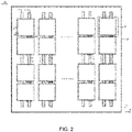
- a light-emitting substrate 100' includes a plurality of light-emitting components 20'.
- Each light-emitting component 20' is coupled to one first power supply voltage signal line LV1' and one second power supply voltage signal line LV2'.
- the first power supply voltage signal line LV1' and the second power supply voltage signal line LV2' respectively transmit a first power supply voltage signal and a second power supply voltage signal to the light-emitting component 20', so as to control an amplitude of a current flowing through the light-emitting component 20'.
- the first power supply voltage signal line LV1' and the second power supply voltage signal line LV2' need to be led out to a surface of a peripheral region of the light-emitting substrate 100' through vias, and then are bonded to an external driving circuit through a flexible circuit board.
- a material in the light-emitting substrate 100' is a hard material (such as glass)
- the number of traces on the light-emitting substrate 100' is large. Limited by a limit distance between gold fingers on the flexible circuit board and a size of the flexible circuit board, the light-emitting substrate 100' needs to be connected to a plurality of flexible circuit boards to meet the requirements, which results in a higher production cost.
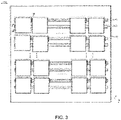
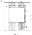
- the light-emitting substrate 100 has a plurality of light-emitting areas S.
- the light-emitting substrate 100 includes a base 10, a plurality of light-emitting components 20, a plurality of first power supply voltage signal lines LV1, and a plurality of first control circuits 30.
- the plurality of light-emitting components 20 are disposed on the base 10, and one light-emitting component 20 is located within one light-emitting area S.
- the plurality of first power supply voltage signal lines LV1 are disposed on the base 10 and arranged at intervals.
- the plurality of first control circuits 30 are disposed on the base 10, each of the first control circuits 30 is coupled to a first electrode of one light-emitting component 20, and each of the first power supply voltage signal lines LV1 is coupled to at least two first control circuits 30.
- the first control circuit 30 is configured to transmit a first power supply voltage signal from the first power supply voltage signal line LV1 to the first electrode of the light-emitting component 20 coupled to the first control circuit 30, so as to control an amplitude of a current flowing through the light-emitting component 20.
- the first power supply voltage signal is a direct current low voltage signal.
- each of the first control circuits 30 in the light-emitting substrate 100 is coupled to a first electrode of one light-emitting component 20, and each first power supply voltage signal line LV1 is coupled to at least two first control circuits 30, which reduces the number of signal lines (for example, the first power supply voltage signal lines LV1) in the light-emitting substrate 100 and a voltage drop on the signal lines, and improves a stability of the signal.
- the first control circuit 30 transmits the first power supply voltage signal to the first electrode of the light-emitting component 20 coupled to the first control circuit 30, and the first power supply voltage signal determines the amplitude of the current transmitted to the light-emitting component 20.
- the first control circuit 30 may control a duration for which the first power supply voltage signal is transmitted to the light-emitting component 20; and the amplitude of the current and the duration together determine a light-emitting brightness of the light-emitting component 20.
- each of the first control circuits 30 is coupled to the first electrode of the light-emitting component 20
- each of the first power supply voltage signal lines LV1 is coupled to at least two first control circuits 30, and the first control circuit 30 transmits the first power supply voltage signal from the first power supply voltage signal line LV1 to the first electrode of the light-emitting component 20 coupled to the first control circuit 30, so as to control the amplitude of the current flowing through the light-emitting component 20 and the duration.
- the first control circuit 30 controls the duration for which the first power supply voltage signal is transmitted to the light-emitting component 20, and the first power supply voltage signal determines the amplitude of the current transmitted to the light-emitting component 20, so that the light-emitting brightness of the light-emitting component 20 can be controlled jointly by the amplitude of the current and the duration.
- the number of the signal lines for example, the first power supply voltage signal lines LV1
- the number of the signal lines for example, the first power supply voltage signal lines LV1
- a width of the signal line may be appropriately increased with a thickness of the signal line reduced, so that an impedance of the signal line and the voltage drop on the signal line are reduced, which improves the stability of the signal.
- a flexible circuit board is used to bond the external driving circuit to the light-emitting substrate 100, since the number of the lines is reduced, the number of flexible circuit boards may be reduced accordingly, so that the production cost is reduced.
- the plurality of light-emitting areas S are arranged in an array, and the plurality of first control circuits 30 are arranged in an array.
- light-emitting areas S arranged in a line in a horizontal direction X are referred to as a row of light-emitting areas
- light-emitting areas S arranged in a line in a vertical direction Y are referred to as a column of light-emitting areas.
- First control circuits 30 arranged in a line in the horizontal direction X are referred to as a row of first control circuits
- first control circuits 30 arranged in a line in the vertical direction Y are referred to as a column of first control circuits.
- light-emitting components 20 in a same row of light-emitting areas S are coupled to one first power supply voltage signal line LV1 through a row of first control circuits 30; alternatively, as shown in FIG. 2 , light-emitting components 20 in a same column of light-emitting areas S are coupled to one first power supply voltage signal line LV1 through a column of first control circuits 30.
- the light-emitting substrate 100 includes light-emitting areas S arranged in n rows and m columns and first control circuits 30 arranged in the n rows and the m columns, where n and m are both positive integers.
- One light-emitting area S corresponds to one first control circuit 30.
- the first power supply voltage signal line LV1 extends in the row direction (i.e., the horizontal direction X in FIG. 3 ), and in this case, the number of the first power supply voltage signal lines LV1 is n.
- the first power supply voltage signal line LV1 extends in the column direction (i.e., the vertical direction Y in FIG. 2 ), and in this case the number of the first power supply voltage signal lines LV1 is m.
- the number of the first power supply voltage signal lines LV1 in the light-emitting substrate 100 in the embodiments of the present disclosure is reduced.
- the number of the first power supply voltage signal lines LV1 is n; and in a case where the first power supply voltage signal lines LV1 extend in the column direction, the number of the first power supply voltage signal lines LV1 is m, which reduces the number of the signal lines of the light-emitting substrate 100, and simplifies the wiring design of the light-emitting substrate 100. Since the number of the signal lines is reduced, a design spacing between the signal lines may be relatively increased. Therefore, the width of the signal line may be appropriately increased to reduce the impedance of the signal line and the voltage drop on the signal line, which improves the stability of the signal.
- the first control circuit 30 is configured to receive a first light-emission signal EM1 and a first enable signal PW1, and transmit a first powers supply voltage signal V1 to the first electrode of the light-emitting component 20 coupled to the first control circuit 30 according to the first light-emission signal EM1 and the first enable signal PW1, so as to control the amplitude of the current flowing through the light-emitting component 20.
- V1 represents the first power supply voltage signal from the first power supply voltage signal line LV1.
- the first light-emission signal EM1 received by the first control circuit 30 is a light-emission data for the light-emitting component 20 coupled to the first control circuit 30.
- the first light-emission signal EM1 includes a pulse width modulation (PWM) signal.
- PWM pulse width modulation
- the first enable signal PW1 received by the first control circuit 30 is a signal for driving the first control circuit 30 to be turned on.
- the first enable signal PW1 includes a power signal.
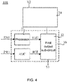
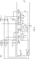
- the first control circuit 30 includes: a processor 31, an analog-to-digital converter ADC and a first output sub-circuit 32.
- the processor 31 is configured to receive the first light-emission signal EM1 and convert a format of the first light-emission signal EM1 to generate a second light-emission signal EM2.
- the processor 31 converts the first light-emission signal EM1 into the second light-emission signal EM2 to match a format of a signal required for an operation of the first control circuit 30.
- a specific conversion manner is not limited here, which can be set by a person skilled in the art according to actual product requirements.
- the first light-emission signal EM1 and the second light-emission signal EM2 may both be PWM signals with different formats.
- the analog-to-digital converter ADC is configured to receive the first enable signal PW1 and generate a reference signal REF.
- the first enable signal PW1 is an analog signal
- the reference signal REF is a digital signal.
- the analog-to-digital converter ADC generates reference signals REF with different potentials according to received first enable signals PW1 with different potentials.
- the first output sub-circuit 32 is configured to transmit the first power supply voltage signal V1 from the first power supply voltage signal line LV1 to the first electrode of the light-emitting component 20 according to the second light-emission signal EM2 from the processor 31 and the reference signal REF from the analog-to-digital converter ADC.
- the first output sub-circuit 32 is turned on under a control of the second light-emission signal EM2 and the reference signal REF, and transmits the first power supply voltage signal to the first electrode of the light-emitting component 20.
- the potential of the second light-emission signal EM2 turn-on duration of the respective first control circuits 30 are not completely the same, so that a duration for which the first power supply voltage signal V1 is transmitted to the first electrode of the light-emitting component 20 can be adjusted and an operating time of the light-emitting component 20 can be controlled.
- the potential of the reference signal REF the amplitude of the current flowing through the light-emitting component 20 can be controlled.
- first enable signals PW1 received by respective first control circuits 30 may be the same or may be different.
- the reference signals REF generated by the respective first control circuits 30 are the same.
- the duration for which the first power supply voltage signal V1 is transmitted to the first electrode of the light-emitting component 20 may be adjusted according to the received different first light-emission signal EM1.
- the reference signals REF generated by the respective first control circuits 30 are different, so that the amplitude of the current flowing through the light-emitting component 20 may be adjusted. Therefore, the brightness of the light-emitting component 20 in the light-emitting area S is adjusted by controlling the amplitude of the current flowing through the light-emitting component 20 and the duration according to the received first enable signal PW1 and the first light-emission signal EM1.
- the first output sub-circuit 32 includes: a first transistor M1, a first resistor R1, a comparator A, and a second transistor M2.
- a control electrode of the first transistor M1 is coupled to the processor 31, and a second electrode of the first transistor M1 is coupled to the first electrode of the light-emitting component 20.
- a first end of the first resistor R1 is coupled to the first power supply voltage signal line LV1.
- a non-inverting input terminal of the comparator A is coupled to an output terminal of the analog-to-digital converter ADC, and an inverting input terminal of the comparator A is coupled to a second end of the first resistor R1.
- a control electrode of the second transistor M2 is coupled to an output terminal of the comparator A, a first electrode of the second transistor M2 is coupled to the second end of the first resistor R1, and a second electrode of the second transistor M2 is coupled to the first electrode of the first transistor M1.
- the comparator A compares the first power supply voltage signal V1 transmitted through the first resistor R1 with the reference signal REF from the analog-to-digital converter ADC, and transmits the compared signal to the second transistor M2 to control a turn-on of the second transistor M2. Since potentials of the first enable signals PW1 received by first control circuits 30 coupled to different light-emitting components 20 are not completely the same, potentials of the reference signals REF generated according to the first enable signals PW1 are not completely the same.
- the reference signals REF whose potentials are not completely the same may be generated by adjusting the potentials of the first enable signals PW1, so as to control the amplitude of the current flowing through the second transistor M2, and control the amplitude of the current flowing through the light-emitting component 20.
- the processor 31 converts the format of the first light-emission signal EM1 to generate the second light-emission signal EM2, and the first transistor M1 is turned on under a control of the second light-emission signal EM2. Since the potentials of the first light-emission signals EM1 corresponding to different light-emitting components 20 are not completely the same, and the potentials of the second light-emission signals EM2 are not completely the same either, a turn-on duration of the first transistor M1 in each first control circuit 30 may be controlled by adjusting the potentials of the first light-emission signals EM1 to generate the second light-emission signals EM2 with potentials which are not completely the same, so as to control the duration for which the first power supply voltage signal V1 is transmitted to the first electrode of the light-emitting component 20 through the first output sub-circuit 32.
- the transistors may be thin film transistors, field-effect transistors or other switching devices with same characteristics, which is not limited in the embodiments of the present disclosure.
- the control electrode of the transistor is a gate of the transistor, the first electrode is one of a source and a drain of the transistor, and the second electrode is the other one of the source and the drain of the transistor. Since the source and the drain of the transistor may be symmetrical in structure, there may be no difference in structure between the source and the drain of the transistor. That is, there may be no difference in structure between the first electrode and the second electrode of the transistor in the embodiments of the present disclosure.
- the first electrode of the transistor is the source, and the second electrode of the transistor is the drain.
- the first electrode of the transistor is the drain, and the second electrode of the transistor is the source.
- the light-emitting substrate 100 includes first control chips 101.
- the first control chip 101 includes the first control circuit 30.
- the first control chip 101 further includes: a first interface P1, a second interface P2, a third interface P3, and a fourth interface P4.
- the first interface P1 is coupled to the processor 31 in the first control circuit 30.
- the second interface P2 is coupled to the analog-to-digital converter ADC in the first control circuit 30.
- the third interface P3 is coupled to the first power supply voltage signal line LV1 and the first output sub-circuit 32 in the first control circuit 30.
- the fourth interface P4 is coupled to the first output sub-circuit 32 in the first control circuit 30 and the first electrode of the light-emitting component 20.
- the first interface P1 is configured to receive the first light-emission signal EM1 and transmit the first light-emission signal EM1 to the processor 31.
- the second interface P2 is configured to receive the first enable signal PW1 and transmit the first enable signal PW1 to the analog-to-digital converter ADC.
- the third interface P3 is configured to receive the first power supply voltage signal V1 from the first power supply voltage signal line LV1 and transmit the first power supply voltage signal to the first output sub-circuit 32.
- the fourth interface P4 is configured to transmit the first power supply voltage signal transmitted through the first output sub-circuit 32 to the first electrode of the light-emitting component 20.
- the first control chip 101 controls the duration for which the first power supply voltage signal V1 is transmitted to a light-emitting component 20 coupled thereto according to the received first light-emission signal EM1 and the first enable signal PW1, so as to control the amplitude of the current flowing through the light-emitting component 20 coupled to the first control chip 101 and the duration.
- the number of interfaces of the first control chip 101 is small, and a size of the first control chip 101 is in an order of micrometer, which causes the first control chip 101 to have a small effect on an area of an effective light-emitting region in the light-emitting substrate 100.
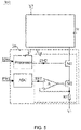
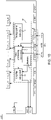
- the light-emitting substrate 100 further includes a second control circuit 40 disposed on the base 10.
- the second control circuit 40 is coupled to the plurality of first control circuits 30.
- the second control circuit 40 is configured to receive a driving signal, and transmit a first light-emission signal EM1 and a first enable signal PW1 to each first control circuit 30 according to the driving signal.
- the second control circuit 40 includes: a timing control sub-circuit 41, a data processing sub-circuit 42, a memory 43, and an amplifier sub-circuit 44.
- the data processing sub-circuit 42 is coupled to the timing control sub-circuit 41 and the plurality of first control circuits 30.
- the amplifier sub-circuit 44 is coupled to the data processing sub-circuit 42, the memory 43 and the plurality of first control circuits 30.
- the timing control sub-circuit 41 is configured to generate a clock signal.
- the data processing sub-circuit 42 is configured to receive the driving signal DRV, output second enable signals PW2 according to the driving signal DRV and the clock signal from the timing control sub-circuit 41, and transmit the first light-emission signals EM1 to the plurality of first control circuits 30.
- the memory 43 is configured to store a timing data and light-emission current data for a preset light-emission mode.
- the light-emitting substrate 100 may set the light-emission mode of the light-emitting substrate 100 according to a display mode of the display apparatus, and store the timing data and light-emission current data for the preset light-emission mode.
- the amplifier sub-circuit 44 is configured to amplify a power of each of the second enable signals PW2 from the data processing sub-circuit 42 according to the timing data and the light-emission current data for the preset light-emission mode, generate the first enable signals PW1, and transmit the first enable signals PW1 to the plurality of first control circuits 30.
- the timing control sub-circuit 41 when the second control circuit 40 starts to operate, the timing control sub-circuit 41 generates the clock signal, and the data processing sub-circuit 42 transmits the first light-emission signals EM1 to the plurality of first control circuits 30 according to the clock signal and the received driving signal DRV, and transmits the second enable signals PW2 to the amplifier sub-circuit 44.
- the amplifier sub-circuit 44 amplifies the powers of the second enable signals PW2 according to the timing data and the light-emission current data for the preset lighting mode stored in the memory 43, generates the first enable signals PW1, transmits the first enable signals PW1 to the plurality of first control circuits 30, and controls the magnitude of the currents of the first control circuits 30 to drive the plurality of first control circuits 30 to operate, so as to realize a control of an operation state of the light-emitting component 20 coupled to each first control circuit 30.
- the amplifier sub-circuit 44 amplifies the power of the second enable signal PW2, which may improve a loading capacity of a second control chip 102.
- the light-emitting substrate 100 includes the second control chip 102. As shown in FIG. 9 , the second control chip 102 includes the second control circuit 40.
- the second control chip 102 further includes: a plurality of enable signal interfaces E, a plurality of light-emission signal interfaces L, and a driving signal interface D.
- the plurality of enable signal interfaces E are coupled to the amplifier sub-circuit 44 in the second control circuit 40, and each enable signal interface E is coupled to at least one first control circuit 30.
- the plurality of light-emission signal interfaces L are coupled to the data processing sub-circuit 42 in the second control circuit 40, and each light-emission signal interface L is coupled to one first control circuit 30.
- the first control circuit 30 in the first row and the first column is coupled to the light-emission signal interface L(1_1)
- the first control circuit 30 in the second row and the first column is coupled to the light-emission signal interface L(1_2)
- the first control circuit 30 in the n-th row and the first column is coupled to the light-emission signal interface L(1_n)
- the first control circuit 30 in the first row and the m-th column is coupled to the light-emission signal interface L(m_1)
- the first control circuit 30 in the second row and the m-th column is coupled to the light-emission signal interface L(m_2)
- the first control circuit 30 in the n-th row and the m-th column is coupled to the light-emission signal interface L(m_n).
- the driving signal interface D is coupled to the data processing sub-circuit 42.
- the enable signal interface E is configured to receive the first enable signal PW1 from the amplifier sub-circuit 44, and transmit the first enable signal PW1 to the first control circuit 30 coupled thereto.
- the light-emission signal interface L is configured to receive the first light-emission signal EM1 from the data processing sub-circuit 42, and transmit the first light-emission signal EM1 to the first control circuit 30 coupled thereto.
- the driving signal interface D is configured to receive the driving signal DRV and transmit the driving signal DRV to the data processing sub-circuit 42.
- the driving signal interface D may be a serial peripheral interface (SPI). As shown in FIG. 10 , the driving signal interface D includes a serial clock (SCLK) interface for receiving a serial clock signal generated by a master device, a master output/slave input (MOSI) interface for receiving a data signal transmitted by the master device, and a vertical frame synchronization signal interface Vsync for receiving a vertical frame synchronization signal transmitted by the master device. That is, the driving signal DRV received by the driving signal interface D includes the SCLK signal, the MOSI signal, and the vertical frame synchronization signal Vsync.
- SCLK serial clock
- MOSI master output/slave input
- Vsync vertical frame synchronization signal transmitted by the master device
- the master device is the display apparatus
- a slave device is the second control chip 102.
- the driving signal received by the driving signal interface D may be from a system on chip (SOC) or a timing controller (T-con) in the display apparatus.
- the second control chip 102 further includes a control signal interface EN, a master input/slave output (MISO) interface, and a chip select (CS) interface.
- the control signal interface EN is used to receive a control signal from the master device to control the second control chip 102 to start operating. For example, when the signal received by the control signal interface EN is of a high level, the second control chip 102 starts to operate, and when the signal received by the control signal interface EN is of a low level, the second control chip 102 stops working.
- the MISO interface is used to transmit data from the second control chip 102 to the master device.
- a signal received by the CS interface is used to drive the second control chip 102 to start transmitting data. For example, when the signal received by the CS interface is of an active low level, the second control chip 102 performs a data transmission.
- each of the enable signal interfaces E is coupled to a row or a column of first control circuits 30.
- each of the enable signal interfaces E is coupled to a row of first control circuits 30, the signal output by each of the enable signal interfaces E may control operations of the row of the first control circuits 30; and in a case where each of the enable signal interfaces E is coupled to a column of first control circuits 30, the signal output by each of the enable signal interfaces E may control operations of the column of the first control circuits 30.
- one enable signal interface E may be coupled to a row of first control circuits 30.
- the first control circuits in the first row are coupled to the enable signal interface E(1)
- the first control circuits in the second row are coupled to the enable signal interface E(2)
- the first control circuits in the n-th row are coupled to the enable signal interface E(n).
- the light-emitting substrate 100 further includes a plurality of second power supply voltage signal lines LV2.
- the plurality of second power supply voltage signal lines LV2 are disposed on the base 10 and arranged at intervals.
- Second electrodes of light-emitting components 20 in at least two light-emitting areas S are coupled to one second power supply voltage signal line LV2.
- the second power supply voltage signal line LV2 is configured to transmit a second power supply voltage signal to the second electrode of the light-emitting component 20 coupled thereto.
- V2 represents the second power supply voltage signal from the second power supply voltage signal line LV2.
- the second power supply voltage signal V2 is a direct current high voltage signal.
- an operating duration of the light-emitting component 20 can be controlled by controlling a duration for which the first power supply voltage signal V1 is transmitted to the light-emitting component 20 by the first control circuit 30.
- the second electrodes of the light-emitting components 20 in at least two light-emitting areas S in the light-emitting substrate 100 are coupled to one second power supply voltage signal line LV2, so that the number of second power supply voltage signal lines LV2 is reduced, and a wiring design of the light-emitting substrate 100 is simplified.
- the width of the signal line may be appropriately increased to reduce the impedance of the signal line and the voltage drop on the signal line, which improves the stability of the signal.
- the flexible circuit board is used to bond the light-emitting substrate 100 to the external driving circuit, since the number of the lines is reduced, the number of the flexible circuit boards is also reduced accordingly, so that the production cost is reduced.
- light-emitting components 20 in a same row or a same column of light-emitting area are coupled to one second power supply voltage signal line LV2.
- the light-emitting substrate 100 includes the light-emitting areas S arranged in the n rows and the m columns and the first control circuits 30 arranged in the n rows and the m columns.
- the second power supply voltage signal line LV2 extends in the row direction (the horizontal direction X shown in FIG. 3 ), and in this case, the number of the second power supply voltage signal lines LV2 is n.
- the number of the second power supply voltage signal lines LV2 is n.
- the second power supply voltage signal line LV2 extends in the column direction (the vertical direction Y shown in FIG. 2 ), and in this case, the number of the second power supply voltage signal lines LV2 is m.
- the number of the second power supply voltage signal lines LV2 in the light-emitting substrate 100 in the embodiments of the present disclosure is reduced.
- the number of the second power supply voltage signal lines LV2 is n; and in a case where the second power supply voltage signal lines LV2 extend in the column direction, the number of the second power supply voltage signal lines LV2 is m, which reduces the number of the signal lines of the light-emitting substrate 100. Since the number of the signal lines is reduced, the spacing between the signal lines is relatively increased. Therefore, the width of the signal line may be appropriately increased to reduce the impedance of the signal line and the voltage drop on the signal line, which improves the stability of the signal. Moreover, in the case where the flexible circuit board is used to bond the light-emitting substrate 100 to the external driving circuit, since the number of the lines is reduced, the number of the flexible circuit boards is also reduced accordingly, so that the production cost is reduced.
- the first power supply voltage signal line LV1 and the second power supply voltage signal line LV2 both extend in the column direction, or both extend in the row direction.
- the light-emitting substrate 100 includes the light-emitting areas S arranged in the n rows and the m columns and the first control circuits 30 arranged in the n rows and the m columns, and the first power supply voltage signal lines LV1 and the second power supply voltage signal lines LV2 extend in the row direction.
- a total number of the first power supply voltage signal lines LV1 and the second power supply voltage signal lines LV2 is (2 ⁇ n).
- the first power supply voltage signal lines LV1 and the second power supply voltage signal lines LV2 extend in the column direction, and in this case, a total number of the first power supply voltage signal lines LV1 and the second power supply voltage signal lines LV2 is (2 ⁇ m).
- the number of the first power supply voltage signal lines LV1 and the number of the second power supply voltage signal lines LV2 in the light-emitting substrate 100 in the embodiments of the present disclosure are reduced.
- the total number of the first power supply voltage signal lines LV1 and the second power supply voltage signal lines LV2 is (2 ⁇ n)
- the total number of the first power supply voltage signal lines LV1 and the second power supply voltage signal lines LV2 is (2 ⁇ m)
- the width of the signal line may be appropriately increased to reduce the impedance of the signal line and the voltage drop on the signal line, which improves the stability of the signal.
- the flexible circuit board is used to bond the external driving circuit to the light-emitting substrate 100, since the number of the lines is reduced, the number of the flexible circuit boards is also reduced accordingly, so that the production cost is reduced.
- the second power supply voltage signal line LV2 and the first power supply voltage signal line LV1 are of a same material and are disposed in a same layer.
- the second power supply voltage signal line LV2 and the first power supply voltage signal line LV1 may be formed simultaneously, thereby simplifying the production process.
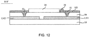
- the light-emitting substrate 100 further includes an insulating layer 50.
- the first power supply voltage signal line LV1 and the second power supply voltage signal line LV2 are located on a side, proximate to the base 10, of the insulating layer 50, and the light-emitting component 20 and the first control circuit 30 are located on a side, away from the base 10, of the insulating layer 50.
- the insulating layer 50 is provided with first vias 51 and second vias 52.
- the first control circuit 30 is coupled to the first power supply voltage signal line LV1 through a first via 51, and the second electrode of the light-emitting component 20 is coupled to the second power supply voltage signal line LV2 through a second via 52.
- the light-emitting substrate 100 further includes connection patterns 103 disposed on the side, away from the base 10, of the insulating layer 50, and the connection patterns 103 cover the first vias 51 and the second vias 52.
- the first control circuit 30 is coupled to the first power supply voltage signal line LV1 through a connection pattern 103 and the first via 51, and the first control circuit 30 is further coupled to the first electrode of the light-emitting component 20 through the connection pattern 103.
- the second electrode of the light-emitting component 20 is coupled to the second power supply voltage signal line LV2 through a connection pattern 103 and the second via 52.
- the insulating layer 50 may be of an inorganic material including silicon nitride (Si x N y ) or silicon oxide (SiO x ).
- the light-emitting substrate 100 further includes the second control circuit 40, the light-emitting substrate 100 further includes a plurality of connecting leads 60 disposed on the side, away from the base 10, of the insulating layer 50.
- the plurality of connecting leads 60 are configured to couple respective first control circuits 30 with the second control circuit 40.
- a part of the plurality of connecting leads 60 are used to couple the enable signal interfaces E in the second control chip 102 with second interfaces P2 in each row of first control chips 101, and the other part of the plurality of connecting leads 60 are used to couple the light-emission signal interfaces L in the second control chip 102 with first interfaces P1 in the first control chips 101.
- the second interfaces P2 in the first control chips 101 in the first row are coupled to the enable signal interface E(1) in the second control chip 102 through the connecting lead 60, and the second interfaces P2 in the first control chips 101 in the n-th row are coupled to the enable signal interface E(n) in the second control chip 102 through the connecting lead 60; and the first interface P1 in the first control chip 101 in the first row and the first column is coupled to the light-emission signal interface L(1_1) in the second control chip 102 through the connecting lead 60, and the first interface P1 in the first control chip 101 in the n-th row and the m-th column is coupled to the light-emission signal interface L(m_n) in the second control chip 102 through the connecting lead 60.
- connection lead 60 may be of a metal material including copper (Cu) or aluminum (Al).
- the light-emitting component 20 includes: a plurality of light-emitting devices 21 and a plurality of conductive patterns 22.
- the plurality of light-emitting devices 21 are arranged in an array.
- the plurality of conductive patterns 22 sequentially connect the plurality of light-emitting devices 21 in series.
- a cathode of one of two light-emitting devices 31 located at both ends of the line is the first electrode of the light-emitting component 20, and an anode of the other light-emitting device 31 of the two light-emitting devices is the second electrode of the light-emitting component 20.
- the light-emitting device 31 may be an inorganic light-emitting device including a micro light-emitting diode (micro LED) or a mini light-emitting diode (mini LED).
- micro LED micro light-emitting diode
- mini LED mini light-emitting diode
- the plurality of light-emitting devices 21 are sequentially connected, which may mean that the plurality of light-emitting devices 21 are connected in series with each other.
- the plurality of light-emitting devices 21 may be connected in parallel with each other; alternatively, a part of the plurality of light-emitting devices 21 are connected in series and then connected in parallel with the other part of the light-emitting devices 21.
- Those skilled in the art can select a connection manner of the light-emitting devices 21 in the light-emitting area S according to actual conditions, which is not limited in the present disclosure.
- a shape of each of conductive pattern(s) 22 connecting light-emitting devices 21 in series in a same row is in a fold line shape, and a shape of each of conductive pattern(s) 22 connecting light-emitting devices 21 in series in a same column is in a stripe shape;
- the shape of each of the conductive pattern(s) 22 connecting the light-emitting devices 21 in series in the same column is in the fold line shape, and the shape of each of the conductive pattern(s) 22 connecting the light-emitting devices 21 in series in the same row is in the stripe shape.
- the plurality of conductive patterns 22 are located on a side, away from the base 10, of the first power supply voltage signal lines LV1 and the second power supply voltage signal lines LV2, and the plurality of conductive patterns 22 are located in a different layer from that of the first power supply voltage signal lines LV1 and the second power supply voltage signal lines LV2, the conductive patterns 22 have little effect on a wiring space of the first power supply voltage signal lines LV1 and the second power supply voltage signal lines LV2.
- widths of the first power supply voltage signal lines LV1 and the second power supply voltage signal lines LV2 are reduced due to a reduction of a wiring gap between the first power supply voltage signal lines LV1 and the second power supply voltage signal lines LV2, which causes impedances of the first power supply voltage signal lines LV1 and the second power supply voltage signal lines LV2 to increase, and affects the signal transmission.
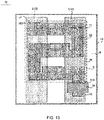
- the conductive patterns 22 and the connection patterns 103 are made of a same material and disposed in a same layer. In terms of process, the conductive patterns 22 and the connection patterns 103 are formed through a same one film forming process. It will be noted that in some embodiments of the present disclosure, the first control circuit 30 may be disposed outside the light-emitting area S and adjacent to the light-emitting component 20. As shown in FIG. 13 , in some other embodiments of the present disclosure, the first control circuit 30 may be directly disposed within the light-emitting area S.
- an orthographic projection of the first control circuit 30 on the base and an orthographic projection of any one of the conductive pattern 22, the connection pattern 103, the light-emitting device 31, the first power supply voltage signal line LV1 and the second power supply voltage signal line LV2 on the base may not overlap.
- the orthographic projection of the first control circuit 30 on the base may partially overlap the orthographic projection of any one of the conductive pattern 22, the connection pattern 103, the light-emitting device 31, the first power supply voltage signal line LV1 and the second power supply voltage signal line LV2 on the base.
- Some embodiments of the present disclosure provide a light-emitting module 200, as shown in FIG. 14 , which includes: the light-emitting substrate 100 as described in any one of the above embodiments, a flexible circuit board 201 and a power supply chip 202.
- the light-emitting substrate 100 includes the first power supply voltage signal lines LV1 and the second power supply voltage signal lines LV2.
- the power supply chip 202 is bonded to the light-emitting substrate 100 through the flexible circuit board 201.
- the power supply chip 202 is configured to transmit the first power supply voltage signal to the first power supply voltage signal line LV1 and transmit the second power supply voltage signal to the second power supply voltage signal line LV2.
- the power supply chip 202 is configured to transmit a third power supply voltage signal and a fourth supply power supply voltage signal to the second control circuit 40.
- the second control chip 102 further includes a third power supply voltage signal interface VDD and a fourth power supply voltage signal interface GND.
- the third power supply voltage signal interface VDD is configured to receive the third power supply voltage signal from the power supply chip 202
- the fourth power supply voltage signal interface GND is configured to receive the fourth power supply voltage signal from the power supply chip 202.
- the third power supply voltage signal is a direct current high voltage signal, such as a signal from a positive pole of a power source
- the fourth power supply voltage signal is a direct current low voltage signal, such as a signal from the negative electrode of the power supply.
- a potential of the third power supply voltage signal is higher than a potential of the second power supply voltage signal.
- a potential of the fourth power supply voltage signal is equal to a potential of the first power supply voltage signal.
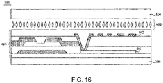
- the embodiments of the present disclosure further provide a display apparatus 300, as shown in FIG. 15 , which includes: the light-emitting module 200 as described in any one of the above embodiments and a driving chip 301.
- the light-emitting substrate 100 in the light-emitting module 200 includes the plurality of first control circuits 30 and the second control circuit 40.
- the driving chip 301 is coupled to the second control circuit 40.
- the driving chip 301 is configured to transmit the driving signal to the second control circuit 40.
- the driving chip 301 may be a SOC or a T-con.
- the driving chip 301 transmits the driving signal to the second control circuit 40.
- the second control circuit 40 receives the driving signal, and transmits the first light-emission signal and the first enable signal to each first control circuit 30 according to the driving signal.
- the first control circuit 30 receives the first light-emission signal and the first enable signal, and transmits the first power supply voltage signal to the first electrode of the light-emitting component 20 coupled to the first control circuit 30 according to the first light-emission signal and the first enable signal, so as to control the amplitude of the current flowing through the light-emitting component 20 and thus to control the light-emitting brightness of the light-emitting component 20.
- the light-emitting module 200 is a backlight module.
- the display apparatus 300 further includes an array substrate 400, a counter substrate 500 and a liquid crystal layer 600.
- the counter substrate 500 is disposed opposite to the array substrate 400, and the light-emitting module 200 is disposed on a side, away from the counter substrate 500, of the array substrate 400.
- the liquid crystal layer 600 is located between the counter substrate 500 and the array substrate 400.
- liquid crystal molecules in the liquid crystal layer 600 are deflected due an action of an electric field formed between a pixel electrode 401 and a common electrode 402 in the array substrate 400, and light emitted by the light-emitting module 200 passes through the liquid crystal layer 600 and exits from a side, away from the light-emitting module 200, of the counter substrate 500.
- the display apparatus 300 can be any apparatus that can display an image, moving (for example a video) or still (for example a static image), literal or graphical. More specifically, it is contemplated that the described embodiments may be implemented in or associated with a variety of electronic apparatus.
- the variety of electronic apparatuses may include (but not limit to), for example, mobile telephones, wireless apparatus, personal data assistant (PAD), hand-held or portable computers, global positioning system (GPS) receivers/navigators, cameras, MPEG-4 Part 14 (MP4) video players, a vidicon, game consoles, watches, clocks, calculators, TV monitors, flat panel displays, computer monitors, car displays (such as odometer display etc.), navigators, cockpit controllers and/or displays, camera view displays (such as rear view camera display in a vehicle), electronic photos, electronic billboards or signages, projectors, building structures, packaging and aesthetic structures (such as a display for an image of a piece of jewelry) etc.
- PDA personal data assistant
- GPS global positioning system
- MP4 MPEG-4 Part 14
- the light-emitting substrate is the light-emitting substrate 100 as described in any one of the above embodiments.
- the light-emitting substrate 100 includes the first control circuits 30 and the second control circuit 40.
- the method for driving the light-emitting substrate 100 includes the following steps.
- the second control circuit 40 receives the driving signal DRV, and transmits the first light-emission signal EM1 and the first enable signal PW1 to each first control circuit 30 according to the driving signal DRV.
- the first control circuit 30 transmits the first power supply voltage signal V1 from the first power supply voltage signal line LV1 to the first electrode of the light-emitting component 20 coupled to the first control circuit 30 according to the first light-emission signal EM1 and the first enable signal PW1, so as to control the amplitude of current flowing through the light-emitting component 20.
- the second control circuit 40 transmits the first light-emission signal EM1 and the first enable signal PW1 to the first control circuit 30 coupled to the light-emitting component 20 in the light-emitting area S according to the driving signal DRV.
- Potentials of the first light-emission signals EM1 received by the first control circuits 30 coupled to different light-emitting components 20 are not completely the same, and potentials of the first enable signals PW1 received by the first control circuits 30 coupled to the different light-emitting components 20 are not completely the same.
- the first control circuit 30 transmits the first power supply voltage signal V1 to the first electrode of the light-emitting component 20 coupled to the first control circuit 30 according to the first enable signal PW1 and the first light-emission signal EM1.
- the potential of the first light-emission signal EM1 By adjusting the potential of the first light-emission signal EM1, the operating duration of the light-emitting component 20 is controlled, and by adjusting the potential of the first enable signal PW1, the amplitude of the current flowing through the light-emitting component 20 is controlled, so that the light-emitting brightnesses of the light-emitting components 20 in respective light-emitting areas S are controlled.
- transmitting, by the second control circuit 40, the first enable signal PW1 to each first control circuit 30 includes the following step.
- the second control circuit 40 transmits the first enable signal PW1 to each row of first control circuits row by row, so as to control all rows of first control circuits 30 to be turned on sequentially. And a previous row of first control circuits to be turned off before a current row of the control circuits is turned on.
- the plurality of light-emitting areas (S(1_1) ... S(m_n)) are arranged in the n rows and the m columns.
- a light-emitting area S(1_1) is a light-emitting area in the first row and the m-th column
- the light-emitting area S(m_n) is a light-emitting area in the n-th row and the m-th column
- the plurality of first control circuits 30 are arranged in the n rows and the m columns.
- the second control circuit 40 transmits the first enable signals (PW1(1) ...
- the second control circuit 40 transmits the first light-emission signal EM1 to each first control circuit 30. For example, when the first row of first control circuits 30 receive the first enable signal PW1(1), the second control circuit 40 transmits the first light-emission signals EM1 to the first control circuits 30 in the first row from the first column to the m-th column.
- the first control circuit 30 is turned on under the control of the first enable signal PW1 and the first light-emission signal EM1, and transmits the first power supply voltage signal V1 from the first power supply voltage signal line LV1 to the first electrode of the light-emitting component 20 in the light-emitting area S coupled to the first control circuit 30, so as to cause the light-emitting component 20 to operate.
- the enable signal interfaces E in the second control chip 102 are coupled to the second interfaces P2 in the first control chips 101, and each enable signal interface E is coupled to one row of first control circuits 30.
- the enable signal interface E(1) is coupled to the first row of first control circuits 30
- the enable signal interface E(2) is coupled to the second row of first control circuits 30
- the enable signal interface E(n) is coupled to the n-th row of first control circuits 30.
- E(n-1), E(n)) of the second control chip 102 sequentially transmit the first enable signals (PW1(1) ... PW1(n)) to the first control circuits 30 in the first row to the n-th row to control the first control circuits 30 in the first row to the n-th row to be turned on sequentially.
- the light-emission signal interfaces L in the second control chip 102 are coupled to the first interfaces P1 in the first control chips 101, each light-emission signal interface L is coupled to one first control circuit 30, and transmits the first light-emission signal EM1 to the first control circuit 30 coupled thereto.
- the light-emission signal interface L(m_n) is coupled to the first control circuit 30 in the n-th row and the m-th column, and the light-emission signal interface L(m_n) transmits the first light-emission signal corresponding to the light-emitting area S(m_n) in the n-th row and the m-th column to the first control circuit 30 in the n-th row and the m-th column.
- the first control circuit 30 is turned on under the control of the first light-emission signal EM1 and the first enable signal PW1, and transmits the first power supply voltage signal V1 to the first electrode of the light-emitting component 20 coupled thereto to cause the light-emitting component 20 to operate.
- the previous row of first control circuits is turned off before the current row of the first control circuit is turned on.
- the second row of first control circuits 30 is turned on; after the second row of first control circuits 30 is turned off, the third row of first control circuits 30 is turned on; and so on until the (n-1)-th row of first control circuits 30 is turned off, and the n-th row of first control circuits 30 is turned on.
- the light-emitting components 20 in the first row to the n-th row in the light-emitting substrate 100 operate row by row, which shortens the operating duration of each row of light-emitting components 20, and reduces a power consumption of the light-emitting substrate 100.
- transmitting, by the second control circuit 40, the first enable signal PW1 to each first control circuit 30 includes the following step.
- the second control circuit 40 simultaneously transmits the first enable signals PW1 to all rows of first control circuits to control the all rows of first control circuits to be turned on simultaneously. And each row of first control circuits is turned off in the current driving period before each row of first control circuits is turned on in the next driving period.
- the plurality of first control circuits 30 are arranged in the n rows and the m columns.
- the second control circuit 40 simultaneously transmits the first enable signals PW1 to the first control circuits 30 from the first row to the n-th row, and controls all row of first control circuits 30 to be turned on simultaneously.
- the second control circuit 40 transmits the first light-emission signal EM1 to each first control circuit 30.
- the first control circuit 30 is turned on under the control of the first enable signal PW1 and the first light-emission signal EM1, and transmits the first power supply voltage signal V1 from the first power supply voltage signal line LV1 to the first electrode of the light-emitting component 20 in the light-emitting area S coupled to the first control circuit 30, so as to cause the light-emitting component 20 to operate.
- each enable signal interface E is coupled to a row of first control circuits 30, the plurality of enable signal interfaces (E(1), E(2) ... E(n-1), E(n)) of the second control chip 102 simultaneously transmit the first enable signals (PW1(1) ... PW1(n)) to the first control circuits 30 in the first row to the n-th row, so as to control the first control circuits 30 in the first row to the n-th row to be turned on simultaneously.
- Each light-emission signal interface L in the second control chip 102 is coupled to one first control circuit 30, and transmit the first light-emission signal EM1 to the first control circuit 30 coupled thereto.
- the first control circuit 30 is turned on under the control of the first light-emission signal PW1 and the first enable signal EM1, and transmits the first power supply voltage signal V1 to the first electrode of the light-emitting component 20 coupled thereto to cause the light-emitting component 20 to operate.
- transmitting, by the second control circuit 40, the first enable signal PW1 to each first control circuit 30 includes the following step.
- the second control circuit 40 sequentially transmits the first enable signal PW1 to each row of first control circuits to control all rows of first control circuits to be turned on sequentially. And each row of first control circuits is turned off in the current driving period before each row of first control circuits is turned on in the next driving period.
- the plurality of first control circuits 30 are arranged in the n rows and the m columns.
- the second control circuit 40 transmits the first enable signals (PW1(1) ... PW1(n)) row by row to the first control circuits 30 from the first row to the n-th row, and controls all rows of first control circuits 30 to be turned on sequentially.
- the second control circuit 40 transmits the first light-emission signal EM1 to each first control circuit 30, the first control circuit 30 is turned on under the control of the first enable signal PW1 and the first light-emission signal EM1, and transmits the first power supply voltage signal V1 from the first power supply voltage signal line LV1 to the first electrode of the light-emitting component 20 in the light-emitting area S coupled to the first control circuit 30 to cause the light-emitting component 20 to operate.
- each enable signal interface E is coupled to a row of first control circuits 30, the plurality of enable signal interfaces (E(1), E(2) ... E(n-1), E(n)) of the second control chip 102 sequentially transmit the first enable signals (PW1(1) ... PW1(n)) to the first control circuits 30 in the first row to the n-th row to control the first control circuits 30 in the first row to the n-th row to be turned on sequentially.
- Each light-emission signal interface L in the second control chip 102 is coupled to a first control circuit 30, and transmits the first light-emission signal EM1 to the first control circuit 30 coupled thereto.
- the first control circuit 30 is turned on under the control of the first light-emission signal EM1 and the first enable signal PW1, and transmits the first power supply voltage signal V1 to the first electrode of the light-emitting component 20 coupled thereto to cause the light-emitting component 20 to operate.
- each row of first control circuits is turned off in the current driving period before each row of first control circuits is turned on in the next driving period.
- the first control circuits 30 in the first row to the n-th row are turned on sequentially, and the operating durations of the first control circuits 30 in the first row to the n-th row are the same.
- each row of first control circuits 30 is delayed to be turned on at the beginning of a driving period.
- the enable signal interface E(1) transmits the first enable signal to the first row of first control circuits 30 coupled thereto, so that there is a first delay time t1 for turning on the first row of first control circuits 30.
- the enable signal interface E(1) transmits the first enable signal to the first row of first control circuits 30 coupled thereto, so that there is a second delay time t2 for turning off the first row of the first control circuit 30.
- a state of the liquid crystal molecules may be adjusted in the first delay time t1 and the second delay time t2, so that the liquid crystal molecule is in a stable state when the light-emitting component 20 operates, which avoids a ghosting problem on a displayed image due to unstable liquid crystal molecules when the light-emitting component 20 operates, and improves a display performance.
- a light-emitting duration of the light-emitting component 20 may be guaranteed, and loss of electro optic conversion efficiency may be reduced.
- the first enable signal transmitted by the enable signal interface E(1) to the first row of first control circuits 30 coupled thereto is represented by PW1(1)
- the first enable signal transmitted by the enable signal interface E(2) to the second row of first control circuit 30s coupled thereto is represented by PW1(2)
- the first enable signal transmitted by the enable signal interface E(n) to the n-th row of first control circuit 30 coupled thereto is represented by PW1(n).
- the vertical frame synchronization signal received by the vertical frame synchronization signal interface Vsync is also represented by Vsync, but the same reference number does not mean that the two are the same component.
- the first control circuit 30 includes the processor 31, the analog-to-digital converter ADC and the first output sub-circuit 32.
- transmitting, by the first control circuit 30, the first power supply voltage signal V1 from the first power supply voltage signal line LV1 to the first electrode of the light-emitting component 20 coupled to the first control circuit 30 according to the first light-emission signal EM1 and the first enable signal PW1 includes:
- the first output sub-circuit 32 is turned on under the control of the second light-emission signal EM2 and the reference signal REF, and transmits the first power supply voltage signal V1 to the first electrode of the light-emitting component 20. Since the potentials of the second light-emission signals EM2 generated by respective first control circuits 30 are not completely the same, and the potentials of the reference signals REF generated by the respective first control circuits 30 are not completely the same, the duration for which the first power supply voltage signal V1 is transmitted to the first electrode of the light-emitting component 20 by the first control circuit 30 may be controlled by adjusting the potential of the second light-emission signal EM2, and then the operating time of the light-emitting component 20 is controlled, and the amplitude of the current flowing through the light-emitting component 20 is controlled by adjusting the potential of the reference signal REF.
- the second control circuit 40 includes the timing control sub-circuit 41, the data processing sub-circuit 42, the memory 43 and the amplifier sub-circuit 44.
- receiving the driving signal DRV, by the second control circuit 40, and transmitting, by the second control circuit 40, the first light-emission signal EM1 and the first enable signal PW1 to each first control circuit 30 according to the driving signal DRV includes:
- the timing control sub-circuit 41 when the second control circuit 40 starts to operate, the timing control sub-circuit 41 generates the clock signal, and the data processing sub-circuit 42 transmits the first light-emission signals EM1 to the plurality of first control circuits 30 according to the clock signal and the received driving signal DRV, and transmits the second enable signals PW2 to the amplifier sub-circuit 44.
- the amplifier sub-circuit 44 amplifies the power of each of the second enable signals PW2 according to the timing data and the light-emission current data for the preset lighting mode stored in the memory 43, generates the first enable signals PW1, transmits the first enable signals PW1 to the plurality of first control circuits 30, and controls the magnitude of the current of each first control circuit 30 to drive the plurality of first control circuits 30 to operate, so as to realize a control of an operation state of the light-emitting component 20 coupled to the first control circuit 30.
Landscapes
- Engineering & Computer Science (AREA)
- Computer Hardware Design (AREA)
- General Physics & Mathematics (AREA)
- Theoretical Computer Science (AREA)
- Physics & Mathematics (AREA)
- Control Of Indicators Other Than Cathode Ray Tubes (AREA)
- Devices For Indicating Variable Information By Combining Individual Elements (AREA)
- Led Devices (AREA)
- Led Device Packages (AREA)
- Arrangement Of Elements, Cooling, Sealing, Or The Like Of Lighting Devices (AREA)
- Circuit Arrangement For Electric Light Sources In General (AREA)
- Liquid Crystal (AREA)
- Electroluminescent Light Sources (AREA)
- Control Of El Displays (AREA)
Applications Claiming Priority (1)
| Application Number | Priority Date | Filing Date | Title |
|---|---|---|---|
| PCT/CN2020/077881 WO2021174473A1 (zh) | 2020-03-05 | 2020-03-05 | 发光基板及其驱动方法、发光模组、显示装置 |
Publications (3)
| Publication Number | Publication Date |
|---|---|
| EP4099088A1 true EP4099088A1 (de) | 2022-12-07 |
| EP4099088A4 EP4099088A4 (de) | 2023-06-14 |
| EP4099088B1 EP4099088B1 (de) | 2025-09-17 |
Family
ID=77613798
Family Applications (1)
| Application Number | Title | Priority Date | Filing Date |
|---|---|---|---|
| EP20922728.9A Active EP4099088B1 (de) | 2020-03-05 | 2020-03-05 | Lichtemittierendes substrat und ansteuerverfahren dafür, lichtemittierendes modul und anzeigevorrichtung |
Country Status (6)
| Country | Link |
|---|---|
| US (1) | US11357083B2 (de) |
| EP (1) | EP4099088B1 (de) |
| JP (1) | JP7497445B2 (de) |
| KR (1) | KR102725682B1 (de) |
| CN (1) | CN113614625B (de) |
| WO (1) | WO2021174473A1 (de) |
Families Citing this family (9)
| Publication number | Priority date | Publication date | Assignee | Title |
|---|---|---|---|---|
| EP3905326B1 (de) * | 2020-04-28 | 2023-01-04 | Nichia Corporation | Lichtemittierende vorrichtung |
| CN114185200B (zh) * | 2021-12-13 | 2022-11-08 | Tcl华星光电技术有限公司 | 光源模块及显示装置 |
| CN114397781A (zh) * | 2021-12-21 | 2022-04-26 | 苏州华星光电技术有限公司 | 背光模组及其制备方法和显示装置 |
| US12293698B2 (en) | 2022-04-26 | 2025-05-06 | Fuzhou Boe Optoelectronics Technology Co., Ltd. | Method for driving light-emitting substrate with light-emitting sub-regions, driving circuit and display apparatus |
| CN114967231B (zh) * | 2022-05-16 | 2024-07-09 | 高创(苏州)电子有限公司 | 发光组件、背光模组及其驱动方法、显示装置 |
| TWI823609B (zh) * | 2022-10-12 | 2023-11-21 | 友達光電股份有限公司 | 顯示裝置及其操作方法 |
| WO2024108403A1 (zh) * | 2022-11-22 | 2024-05-30 | 京东方科技集团股份有限公司 | 显示装置及其驱动电路、驱动方法 |
| DE112023005855T5 (de) * | 2023-02-23 | 2025-12-11 | Boe Technology Group Co., Ltd. | Lichtemittierendes Substrat und lichtemittierende Vorrichtung |
| CN117497677A (zh) * | 2023-03-31 | 2024-02-02 | 惠州华星光电显示有限公司 | 背光模组及显示装置 |
Family Cites Families (15)
| Publication number | Priority date | Publication date | Assignee | Title |
|---|---|---|---|---|
| JP2005252222A (ja) * | 2004-02-03 | 2005-09-15 | Matsushita Electric Ind Co Ltd | 半導体発光装置、照明モジュール、照明装置、表示素子、および半導体発光装置の製造方法 |
| JP4494298B2 (ja) * | 2005-06-24 | 2010-06-30 | シャープ株式会社 | 駆動回路 |
| CN101442856B (zh) * | 2007-11-22 | 2012-04-04 | 宇威光电股份有限公司 | 发光装置 |
| JP5642347B2 (ja) * | 2008-03-07 | 2014-12-17 | ミツミ電機株式会社 | 液晶バックライト装置 |
| WO2011071559A1 (en) * | 2009-12-09 | 2011-06-16 | Nano And Advanced Materials Institute Limited | Method for manufacturing a monolithic led micro-display on an active matrix panel using flip-chip technology and display apparatus having the monolithic led micro-display |
| TWI429331B (zh) * | 2010-07-23 | 2014-03-01 | Au Optronics Corp | 發光二極體驅動方法及驅動電路 |
| US9153171B2 (en) * | 2012-12-17 | 2015-10-06 | LuxVue Technology Corporation | Smart pixel lighting and display microcontroller |
| KR102126534B1 (ko) * | 2013-10-31 | 2020-06-25 | 엘지디스플레이 주식회사 | 광원 구동장치 및 이를 이용한 액정표시장치 |
| CN104637447B (zh) * | 2015-02-06 | 2017-06-27 | 京东方科技集团股份有限公司 | 数据驱动电路、电学补偿方法、阵列基板及显示装置 |
| JP2016148744A (ja) * | 2015-02-12 | 2016-08-18 | 株式会社半導体エネルギー研究所 | 発光パネル、表示モジュール、表示装置 |
| CN105609058B (zh) | 2016-01-04 | 2018-09-04 | 京东方科技集团股份有限公司 | 背光源及显示装置 |
| JP2018124458A (ja) * | 2017-02-01 | 2018-08-09 | パナソニック液晶ディスプレイ株式会社 | 液晶バックライト装置及び表示装置 |
| CN108957852A (zh) * | 2018-07-16 | 2018-12-07 | 上海中航光电子有限公司 | 显示模组和显示装置 |
| US10885830B2 (en) * | 2018-07-24 | 2021-01-05 | Innolux Corporation | Electronic device capable of reducing color shift |
| CN110164879B (zh) * | 2019-07-03 | 2022-04-22 | 京东方科技集团股份有限公司 | 阵列基板、显示装置 |
-
2020
- 2020-03-05 CN CN202080000224.6A patent/CN113614625B/zh active Active
- 2020-03-05 KR KR1020227017340A patent/KR102725682B1/ko active Active
- 2020-03-05 EP EP20922728.9A patent/EP4099088B1/de active Active
- 2020-03-05 WO PCT/CN2020/077881 patent/WO2021174473A1/zh not_active Ceased
- 2020-03-05 US US17/255,060 patent/US11357083B2/en active Active
- 2020-03-05 JP JP2022547796A patent/JP7497445B2/ja active Active
Also Published As
| Publication number | Publication date |
|---|---|
| JP2023525189A (ja) | 2023-06-15 |
| CN113614625B (zh) | 2022-09-13 |
| EP4099088B1 (de) | 2025-09-17 |
| US20220053615A1 (en) | 2022-02-17 |
| US11357083B2 (en) | 2022-06-07 |
| CN113614625A (zh) | 2021-11-05 |
| KR20220150271A (ko) | 2022-11-10 |
| WO2021174473A9 (zh) | 2022-07-14 |
| WO2021174473A1 (zh) | 2021-09-10 |
| KR102725682B1 (ko) | 2024-11-05 |
| JP7497445B2 (ja) | 2024-06-10 |
| EP4099088A4 (de) | 2023-06-14 |
Similar Documents
| Publication | Publication Date | Title |
|---|---|---|
| EP4099088B1 (de) | Lichtemittierendes substrat und ansteuerverfahren dafür, lichtemittierendes modul und anzeigevorrichtung | |
| CN111048041B (zh) | 像素电路及其驱动方法、显示面板和显示装置 | |
| CN111128079B (zh) | 像素电路及其驱动方法、显示面板和显示装置 | |
| US9318047B2 (en) | Organic light emitting display unit structure and organic light emitting display unit circuit | |
| EP4145434B1 (de) | Pixelschaltung und ansteuerungsverfahren dafür, anzeigetafel und anzeigevorrichtung | |
| KR101281926B1 (ko) | 액정표시장치 | |
| WO2021223579A1 (zh) | 像素驱动电路及驱动方法、移位寄存器电路、显示装置 | |
| CN108122524B (zh) | 具有集成型扫描驱动器的显示装置 | |
| KR100449305B1 (ko) | 표시 모듈 | |
| WO2015140861A1 (ja) | 画像表示装置及び表示制御方法 | |
| CN114141204A (zh) | 背光驱动电路及显示装置 | |
| CN115050301A (zh) | 一种显示面板及显示装置 | |
| WO2022110238A1 (zh) | 发光基板及显示装置 | |
| WO2022104752A1 (zh) | 发光基板及显示装置 | |
| WO2023205935A1 (zh) | 电子设备及显示驱动方法 | |
| CN112967681B (zh) | 一种驱动电路、发光组件和显示装置 | |
| TWI853332B (zh) | 驅動器電路及其驅動方法、陣列基板、顯示裝置 | |
| KR20190067454A (ko) | 소스 드라이버 ic 및 이를 포함하는 유기 발광 표시 장치 | |
| US11488543B2 (en) | Gate driving circuit and display device | |
| CN111179864B (zh) | 像素驱动电路及其驱动方法、显示装置、电子设备 | |
| WO2025140633A1 (zh) | 集成电路板、显示装置、显示设备和显示方法 | |
| KR20200089328A (ko) | 액정 표시 패널 및 그 eoa 모듈 | |
| US20200226979A1 (en) | Display device and electronic apparatus | |
| CN223956271U (zh) | 像素电路、显示面板、显示模组及电子设备 | |
| CN113990252B (zh) | 驱动电路及显示模组 |
Legal Events
| Date | Code | Title | Description |
|---|---|---|---|
| STAA | Information on the status of an ep patent application or granted ep patent |
Free format text: STATUS: THE INTERNATIONAL PUBLICATION HAS BEEN MADE |
|
| PUAI | Public reference made under article 153(3) epc to a published international application that has entered the european phase |
Free format text: ORIGINAL CODE: 0009012 |
|
| STAA | Information on the status of an ep patent application or granted ep patent |
Free format text: STATUS: REQUEST FOR EXAMINATION WAS MADE |
|
| 17P | Request for examination filed |
Effective date: 20220729 |
|
| AK | Designated contracting states |
Kind code of ref document: A1 Designated state(s): AL AT BE BG CH CY CZ DE DK EE ES FI FR GB GR HR HU IE IS IT LI LT LU LV MC MK MT NL NO PL PT RO RS SE SI SK SM TR |
|
| REG | Reference to a national code |
Ref legal event code: R079 Free format text: PREVIOUS MAIN CLASS: G02F0001133570 Ipc: G09G0003320000 Ref country code: DE Ref legal event code: R079 Ref document number: 602020059175 Country of ref document: DE Free format text: PREVIOUS MAIN CLASS: G02F0001133570 Ipc: G09G0003320000 |
|
| RIC1 | Information provided on ipc code assigned before grant |
Ipc: H01L 25/16 19740701ALI20230112BHEP Ipc: H05B 33/26 19680901ALI20230112BHEP Ipc: G09G 3/34 19800101ALI20230112BHEP Ipc: G02F 1/13357 20000101ALI20230112BHEP Ipc: G09G 3/32 19800101AFI20230112BHEP |
|
| A4 | Supplementary search report drawn up and despatched |
Effective date: 20230517 |
|
| DAV | Request for validation of the european patent (deleted) | ||
| DAX | Request for extension of the european patent (deleted) | ||
| RIC1 | Information provided on ipc code assigned before grant |
Ipc: H01L 25/16 20060101ALI20230511BHEP Ipc: H05B 33/26 20060101ALI20230511BHEP Ipc: G09G 3/34 20060101ALI20230511BHEP Ipc: G02F 1/13357 20060101ALI20230511BHEP Ipc: G09G 3/32 20160101AFI20230511BHEP |
|
| GRAP | Despatch of communication of intention to grant a patent |
Free format text: ORIGINAL CODE: EPIDOSNIGR1 |
|
| STAA | Information on the status of an ep patent application or granted ep patent |
Free format text: STATUS: GRANT OF PATENT IS INTENDED |
|
| INTG | Intention to grant announced |
Effective date: 20250519 |
|
| GRAS | Grant fee paid |
Free format text: ORIGINAL CODE: EPIDOSNIGR3 |
|
| GRAA | (expected) grant |
Free format text: ORIGINAL CODE: 0009210 |
|
| STAA | Information on the status of an ep patent application or granted ep patent |
Free format text: STATUS: THE PATENT HAS BEEN GRANTED |
|
| AK | Designated contracting states |
Kind code of ref document: B1 Designated state(s): AL AT BE BG CH CY CZ DE DK EE ES FI FR GB GR HR HU IE IS IT LI LT LU LV MC MK MT NL NO PL PT RO RS SE SI SK SM TR |
|
| REG | Reference to a national code |
Ref country code: GB Ref legal event code: FG4D |
|
| REG | Reference to a national code |
Ref country code: CH Ref legal event code: EP |
|
| REG | Reference to a national code |
Ref country code: IE Ref legal event code: FG4D |
|
| REG | Reference to a national code |
Ref country code: DE Ref legal event code: R096 Ref document number: 602020059175 Country of ref document: DE |
|
| PG25 | Lapsed in a contracting state [announced via postgrant information from national office to epo] |
Ref country code: NO Free format text: LAPSE BECAUSE OF FAILURE TO SUBMIT A TRANSLATION OF THE DESCRIPTION OR TO PAY THE FEE WITHIN THE PRESCRIBED TIME-LIMIT Effective date: 20251217 |
|
| REG | Reference to a national code |
Ref country code: LT Ref legal event code: MG9D |
|
| PG25 | Lapsed in a contracting state [announced via postgrant information from national office to epo] |
Ref country code: FI Free format text: LAPSE BECAUSE OF FAILURE TO SUBMIT A TRANSLATION OF THE DESCRIPTION OR TO PAY THE FEE WITHIN THE PRESCRIBED TIME-LIMIT Effective date: 20250917 |
|
| PG25 | Lapsed in a contracting state [announced via postgrant information from national office to epo] |
Ref country code: HR Free format text: LAPSE BECAUSE OF FAILURE TO SUBMIT A TRANSLATION OF THE DESCRIPTION OR TO PAY THE FEE WITHIN THE PRESCRIBED TIME-LIMIT Effective date: 20250917 |
|
| PG25 | Lapsed in a contracting state [announced via postgrant information from national office to epo] |
Ref country code: GR Free format text: LAPSE BECAUSE OF FAILURE TO SUBMIT A TRANSLATION OF THE DESCRIPTION OR TO PAY THE FEE WITHIN THE PRESCRIBED TIME-LIMIT Effective date: 20251218 |
|
| PG25 | Lapsed in a contracting state [announced via postgrant information from national office to epo] |
Ref country code: SE Free format text: LAPSE BECAUSE OF FAILURE TO SUBMIT A TRANSLATION OF THE DESCRIPTION OR TO PAY THE FEE WITHIN THE PRESCRIBED TIME-LIMIT Effective date: 20250917 |
|
| REG | Reference to a national code |
Ref country code: NL Ref legal event code: MP Effective date: 20250917 |
|
| PG25 | Lapsed in a contracting state [announced via postgrant information from national office to epo] |
Ref country code: LV Free format text: LAPSE BECAUSE OF FAILURE TO SUBMIT A TRANSLATION OF THE DESCRIPTION OR TO PAY THE FEE WITHIN THE PRESCRIBED TIME-LIMIT Effective date: 20250917 |
|
| PG25 | Lapsed in a contracting state [announced via postgrant information from national office to epo] |
Ref country code: BG Free format text: LAPSE BECAUSE OF FAILURE TO SUBMIT A TRANSLATION OF THE DESCRIPTION OR TO PAY THE FEE WITHIN THE PRESCRIBED TIME-LIMIT Effective date: 20250917 |
|
| PG25 | Lapsed in a contracting state [announced via postgrant information from national office to epo] |
Ref country code: RS Free format text: LAPSE BECAUSE OF FAILURE TO SUBMIT A TRANSLATION OF THE DESCRIPTION OR TO PAY THE FEE WITHIN THE PRESCRIBED TIME-LIMIT Effective date: 20251217 |
|
| PG25 | Lapsed in a contracting state [announced via postgrant information from national office to epo] |
Ref country code: NL Free format text: LAPSE BECAUSE OF FAILURE TO SUBMIT A TRANSLATION OF THE DESCRIPTION OR TO PAY THE FEE WITHIN THE PRESCRIBED TIME-LIMIT Effective date: 20250917 |
|
| REG | Reference to a national code |
Ref country code: AT Ref legal event code: MK05 Ref document number: 1839065 Country of ref document: AT Kind code of ref document: T Effective date: 20250917 |
|
| PG25 | Lapsed in a contracting state [announced via postgrant information from national office to epo] |
Ref country code: SM Free format text: LAPSE BECAUSE OF FAILURE TO SUBMIT A TRANSLATION OF THE DESCRIPTION OR TO PAY THE FEE WITHIN THE PRESCRIBED TIME-LIMIT Effective date: 20250917 |
|
| PG25 | Lapsed in a contracting state [announced via postgrant information from national office to epo] |
Ref country code: ES Free format text: LAPSE BECAUSE OF FAILURE TO SUBMIT A TRANSLATION OF THE DESCRIPTION OR TO PAY THE FEE WITHIN THE PRESCRIBED TIME-LIMIT Effective date: 20250917 |
|
| PGFP | Annual fee paid to national office [announced via postgrant information from national office to epo] |
Ref country code: DE Payment date: 20260320 Year of fee payment: 7 |
|
| PG25 | Lapsed in a contracting state [announced via postgrant information from national office to epo] |
Ref country code: AT Free format text: LAPSE BECAUSE OF FAILURE TO SUBMIT A TRANSLATION OF THE DESCRIPTION OR TO PAY THE FEE WITHIN THE PRESCRIBED TIME-LIMIT Effective date: 20250917 |
|
| PG25 | Lapsed in a contracting state [announced via postgrant information from national office to epo] |
Ref country code: IT Free format text: LAPSE BECAUSE OF FAILURE TO SUBMIT A TRANSLATION OF THE DESCRIPTION OR TO PAY THE FEE WITHIN THE PRESCRIBED TIME-LIMIT Effective date: 20250917 |
|
| PG25 | Lapsed in a contracting state [announced via postgrant information from national office to epo] |
Ref country code: IS Free format text: LAPSE BECAUSE OF FAILURE TO SUBMIT A TRANSLATION OF THE DESCRIPTION OR TO PAY THE FEE WITHIN THE PRESCRIBED TIME-LIMIT Effective date: 20260117 |