EP4089918A1 - Bulk acoustic wave resonator and manufacturing method, bulk acoustic wave resonator unit, filter and electronic device - Google Patents
Bulk acoustic wave resonator and manufacturing method, bulk acoustic wave resonator unit, filter and electronic device Download PDFInfo
- Publication number
- EP4089918A1 EP4089918A1 EP20896703.4A EP20896703A EP4089918A1 EP 4089918 A1 EP4089918 A1 EP 4089918A1 EP 20896703 A EP20896703 A EP 20896703A EP 4089918 A1 EP4089918 A1 EP 4089918A1
- Authority
- EP
- European Patent Office
- Prior art keywords
- layer
- monocrystalline
- bottom electrode
- resonator
- substrate
- Prior art date
- Legal status (The legal status is an assumption and is not a legal conclusion. Google has not performed a legal analysis and makes no representation as to the accuracy of the status listed.)
- Pending
Links
Images


Classifications
-
- H—ELECTRICITY
- H03—ELECTRONIC CIRCUITRY
- H03H—IMPEDANCE NETWORKS, e.g. RESONANT CIRCUITS; RESONATORS
- H03H9/00—Networks comprising electromechanical or electro-acoustic elements; Electromechanical resonators
- H03H9/15—Constructional features of resonators consisting of piezoelectric or electrostrictive material
- H03H9/17—Constructional features of resonators consisting of piezoelectric or electrostrictive material having a single resonator
- H03H9/171—Constructional features of resonators consisting of piezoelectric or electrostrictive material having a single resonator implemented with thin-film techniques, i.e. of the film bulk acoustic resonator [FBAR] type
-
- H—ELECTRICITY
- H03—ELECTRONIC CIRCUITRY
- H03H—IMPEDANCE NETWORKS, e.g. RESONANT CIRCUITS; RESONATORS
- H03H9/00—Networks comprising electromechanical or electro-acoustic elements; Electromechanical resonators
- H03H9/02—Details
- H03H9/02007—Details of bulk acoustic wave devices
- H03H9/02086—Means for compensation or elimination of undesirable effects
- H03H9/02118—Means for compensation or elimination of undesirable effects of lateral leakage between adjacent resonators
-
- H—ELECTRICITY
- H03—ELECTRONIC CIRCUITRY
- H03H—IMPEDANCE NETWORKS, e.g. RESONANT CIRCUITS; RESONATORS
- H03H3/00—Apparatus or processes specially adapted for the manufacture of impedance networks, resonating circuits, resonators
- H03H3/007—Apparatus or processes specially adapted for the manufacture of impedance networks, resonating circuits, resonators for the manufacture of electromechanical resonators or networks
- H03H3/02—Apparatus or processes specially adapted for the manufacture of impedance networks, resonating circuits, resonators for the manufacture of electromechanical resonators or networks for the manufacture of piezoelectric or electrostrictive resonators or networks
-
- H—ELECTRICITY
- H03—ELECTRONIC CIRCUITRY
- H03H—IMPEDANCE NETWORKS, e.g. RESONANT CIRCUITS; RESONATORS
- H03H9/00—Networks comprising electromechanical or electro-acoustic elements; Electromechanical resonators
- H03H9/02—Details
- H03H9/02007—Details of bulk acoustic wave devices
-
- H—ELECTRICITY
- H03—ELECTRONIC CIRCUITRY
- H03H—IMPEDANCE NETWORKS, e.g. RESONANT CIRCUITS; RESONATORS
- H03H9/00—Networks comprising electromechanical or electro-acoustic elements; Electromechanical resonators
- H03H9/02—Details
- H03H9/05—Holders or supports
- H03H9/0504—Holders or supports for bulk acoustic wave devices
- H03H9/0514—Holders or supports for bulk acoustic wave devices consisting of mounting pads or bumps
- H03H9/0523—Holders or supports for bulk acoustic wave devices consisting of mounting pads or bumps for flip-chip mounting
-
- H—ELECTRICITY
- H03—ELECTRONIC CIRCUITRY
- H03H—IMPEDANCE NETWORKS, e.g. RESONANT CIRCUITS; RESONATORS
- H03H9/00—Networks comprising electromechanical or electro-acoustic elements; Electromechanical resonators
- H03H9/02—Details
- H03H9/05—Holders or supports
- H03H9/10—Mounting in enclosures
- H03H9/1007—Mounting in enclosures for bulk acoustic wave [BAW] devices
- H03H9/105—Mounting in enclosures for bulk acoustic wave [BAW] devices the enclosure being defined by a cover cap mounted on an element forming part of the BAW device
-
- H—ELECTRICITY
- H03—ELECTRONIC CIRCUITRY
- H03H—IMPEDANCE NETWORKS, e.g. RESONANT CIRCUITS; RESONATORS
- H03H9/00—Networks comprising electromechanical or electro-acoustic elements; Electromechanical resonators
- H03H9/15—Constructional features of resonators consisting of piezoelectric or electrostrictive material
- H03H9/17—Constructional features of resonators consisting of piezoelectric or electrostrictive material having a single resonator
- H03H9/171—Constructional features of resonators consisting of piezoelectric or electrostrictive material having a single resonator implemented with thin-film techniques, i.e. of the film bulk acoustic resonator [FBAR] type
- H03H9/172—Means for mounting on a substrate, i.e. means constituting the material interface confining the waves to a volume
- H03H9/173—Air-gaps
-
- H—ELECTRICITY
- H03—ELECTRONIC CIRCUITRY
- H03H—IMPEDANCE NETWORKS, e.g. RESONANT CIRCUITS; RESONATORS
- H03H9/00—Networks comprising electromechanical or electro-acoustic elements; Electromechanical resonators
- H03H9/15—Constructional features of resonators consisting of piezoelectric or electrostrictive material
- H03H9/17—Constructional features of resonators consisting of piezoelectric or electrostrictive material having a single resonator
- H03H9/171—Constructional features of resonators consisting of piezoelectric or electrostrictive material having a single resonator implemented with thin-film techniques, i.e. of the film bulk acoustic resonator [FBAR] type
- H03H9/172—Means for mounting on a substrate, i.e. means constituting the material interface confining the waves to a volume
- H03H9/174—Membranes
-
- H—ELECTRICITY
- H03—ELECTRONIC CIRCUITRY
- H03H—IMPEDANCE NETWORKS, e.g. RESONANT CIRCUITS; RESONATORS
- H03H9/00—Networks comprising electromechanical or electro-acoustic elements; Electromechanical resonators
- H03H9/46—Filters
- H03H9/54—Filters comprising resonators of piezoelectric or electrostrictive material
-
- H—ELECTRICITY
- H03—ELECTRONIC CIRCUITRY
- H03H—IMPEDANCE NETWORKS, e.g. RESONANT CIRCUITS; RESONATORS
- H03H3/00—Apparatus or processes specially adapted for the manufacture of impedance networks, resonating circuits, resonators
- H03H3/007—Apparatus or processes specially adapted for the manufacture of impedance networks, resonating circuits, resonators for the manufacture of electromechanical resonators or networks
- H03H3/02—Apparatus or processes specially adapted for the manufacture of impedance networks, resonating circuits, resonators for the manufacture of electromechanical resonators or networks for the manufacture of piezoelectric or electrostrictive resonators or networks
- H03H2003/021—Apparatus or processes specially adapted for the manufacture of impedance networks, resonating circuits, resonators for the manufacture of electromechanical resonators or networks for the manufacture of piezoelectric or electrostrictive resonators or networks the resonators or networks being of the air-gap type
-
- H—ELECTRICITY
- H03—ELECTRONIC CIRCUITRY
- H03H—IMPEDANCE NETWORKS, e.g. RESONANT CIRCUITS; RESONATORS
- H03H3/00—Apparatus or processes specially adapted for the manufacture of impedance networks, resonating circuits, resonators
- H03H3/007—Apparatus or processes specially adapted for the manufacture of impedance networks, resonating circuits, resonators for the manufacture of electromechanical resonators or networks
- H03H3/02—Apparatus or processes specially adapted for the manufacture of impedance networks, resonating circuits, resonators for the manufacture of electromechanical resonators or networks for the manufacture of piezoelectric or electrostrictive resonators or networks
- H03H2003/023—Apparatus or processes specially adapted for the manufacture of impedance networks, resonating circuits, resonators for the manufacture of electromechanical resonators or networks for the manufacture of piezoelectric or electrostrictive resonators or networks the resonators or networks being of the membrane type
-
- H—ELECTRICITY
- H03—ELECTRONIC CIRCUITRY
- H03H—IMPEDANCE NETWORKS, e.g. RESONANT CIRCUITS; RESONATORS
- H03H9/00—Networks comprising electromechanical or electro-acoustic elements; Electromechanical resonators
- H03H9/02—Details
- H03H9/05—Holders or supports
- H03H9/0538—Constructional combinations of supports or holders with electromechanical or other electronic elements
- H03H9/0547—Constructional combinations of supports or holders with electromechanical or other electronic elements consisting of a vertical arrangement
- H03H9/0561—Constructional combinations of supports or holders with electromechanical or other electronic elements consisting of a vertical arrangement consisting of a multilayered structure
Definitions
- Embodiments of the present disclosure relates to the field of semiconductors, and in particular, to a bulk acoustic wave resonator, a filter having the resonator, a bulk acoustic wave resonator unit, and an electronic apparatus having the resonator or the filter.
- a traditional radio frequency filter cannot meet requirements for high-frequency communication due to limitation on the structure and performance.
- a film bulk acoustic resonator (FBAR) used as a new type of MEMS device is adapted to development of wireless communication systems, such that the FBAR technology becomes a research hotspot in the communication field.
- the FBAR has advantages such as a small volume, light weight, low insertion loss, a wide bandwidth, and a high quality factor, and gradually occupies the market.
- the film bulk acoustic resonator mainly includes a "sandwich" structure composed of electrode-piezoelectric film-electrode, i.e., the piezoelectric film is sandwiched between the two metal electrodes.
- the FBAR converts an input electrical signal into a mechanical resonance through an inverse piezoelectric effect, and then converts the mechanical resonance into an electrical signal output through a piezoelectric effect.
- the film bulk acoustic resonator mainly utilizes a longitudinal piezoelectric coefficient (d33) of the piezoelectric film to generate the piezoelectric effect, and thus mainly operates in a thickness extensional mode in a thickness direction.
- the conventional structure is shown in FIG. 1A , in which a substrate is indicated by 01, a cavity is indicated by 02, a bottom electrode is indicated by 03 and spans both sides of the cavity, a piezoelectric layer is indicated by 04, and a top electrode is indicated by 05.
- piezoelectric films used in the traditional film bulk acoustic resonators are polycrystalline nitride films prepared by physical or chemical deposition techniques such as magnetron sputtering, which have poor piezoelectric property (mainly indicated by a low electromechanical coupling coefficient of the resonator), a high defect density (mainly indicated by a low quality factor of the resonator), and poor heat dissipation (mainly indicated by a low power capacity of the resonator).
- etched inclined end faces 06 are formed at both ends of the bottom electrode of the resonator, as shown in FIG. 1 .
- the etched inclined end face has a generally rough surface, defects in the piezoelectric layer deposited on the inclined end faces at the both ends of the bottom electrode may be further increased as shown in a region d in FIG. 1 . These defects may lead to acoustic loss, thereby reducing a Q-factor of the resonator. Moreover, such the resonator cannot meet technical indexes such as lower insertion loss and larger bandwidth required in future mobile communication technologies.
- a bulk acoustic wave resonator that includes a substrate, an acoustic mirror, a bottom electrode connected to a bottom electrode pin, a top electrode connected to a top electrode pin, and a piezoelectric layer provided between the bottom electrode and the top electrode.
- the piezoelectric layer is a monocrystalline piezoelectric film layer.
- a non-pin end of the top electrode and a non-pin end of the bottom electrode are both spaced apart from an edge of the acoustic mirror in a projection of the resonator in a thickness direction.
- the acoustic mirror is an acoustic mirror cavity arranged at an upper side of the substrate and is a blind hole cavity.
- An embodiment of the present disclosure further relates to a bulk acoustic wave resonator unit, which includes the bulk acoustic wave resonator described above and a packaging substrate.
- the packaging substrate is provided with a circuit device that is electrically connected to the top electrode and the bottom electrode of the resonator, respectively.
- the present disclosure also relates to a method of manufacturing a monocrystalline film bulk acoustic wave resonator.
- the monocrystalline film bulk acoustic wave resonator includes a substrate, an acoustic mirror, a bottom electrode connected to a bottom electrode pin, a top electrode connected to a top electrode pin, and a monocrystalline piezoelectric film layer provided between the bottom electrode and the top electrode.
- the method includes: forming the top electrode in such a manner that a non-pin end of the top electrode is spaced apart from an edge of the acoustic mirror in a projection of the resonator in a thickness direction; and forming the bottom electrode in such a manner that a non-pin end of the bottom electrode is spaced apart from the edge of the acoustic mirror in the projection of the resonator in the thickness direction.
- An embodiment of the present disclosure also relates to a filter, which includes the above monocrystalline film bulk acoustic wave resonator, the above monocrystalline film bulk acoustic wave resonator unit, or the monocrystalline film bulk acoustic wave resonator manufactured by the method described above.
- An embodiment of the present disclosure also relates to an electronic apparatus including the above filter, the above resonator, or the above resonator unit.
- FIG. 1B is a top view of a monocrystalline piezoelectric film bulk acoustic wave resonator according to an exemplary embodiment of the present disclosure.
- the reference sign 16 denotes an air gap or cavity of the monocrystalline film resonator.
- the reference sign 13 denotes a bottom electrode of the monocrystalline film resonator above the air gap.
- the reference sign 12 denotes a monocrystalline piezoelectric film layer of the resonator.
- the reference sign 17 denotes a top electrode of the monocrystalline film resonator above the monocrystalline piezoelectric layer.
- the reference sign 19a denotes an electrode connection structure on the top electrode.
- the reference sign 19b denotes an electrode connection structure on the bottom electrode.
- FIG. 1B it is different from the conventional structure shown in FIG. 1A in that the bottom electrode of the monocrystalline film resonator is located in the cavity in a vertical direction. In the conventional structure, the bottom electrode is located above the cavity in the vertical direction.
- FIG. 1C is a schematic partial sectional view along A-A in FIG. 1B .
- the reference sign 15 denotes a substrate
- the reference sign 16 denotes an air gap or cavity
- the reference sign 13 denotes a bottom electrode
- the reference sign 12 denotes a monocrystalline piezoelectric film layer.
- a surface of the monocrystalline piezoelectric film layer may or may not be provided with a seed layer.
- the reference sign 14 denotes an electrode connection structure of the bottom electrode
- the reference sign 17 denotes a top electrode
- the reference sign 18 denotes a bottom electrode pin layer located on an upper surface of the monocrystalline piezoelectric layer.
- a region where the bottom electrode, the monocrystalline piezoelectric film layer and the top electrode overlap with each other in a thickness direction of the resonator is an effective region of the monocrystalline film resonator, that is, a region indicated by D in FIG. 1C .
- a cavity structure in the related art is generally a through hole passing through the substrate, but the deep etched through hole has disadvantages, such as poor control precision of a cavity shape and dimension, a complex process, complicated electrode connection, and a requirement for an additional packaging process to cover the through hole.
- the acoustic mirror cavity 16 is a blind hole, and in other words, the acoustic mirror cavity is sealed from below. In this way, a process flow is simplified, the cost is reduced, control precision of the shape and dimension is improved, the electrode connection is more reliable, and an additional through-hole packaging process is unnecessary.
- top electrode and the bottom electrode in the effective region are both located within the cavity in the vertical direction.
- a non-pin end of the top electrode and a non-pin end of the bottom electrode are both spaced apart from an edge of the acoustic mirror in a projection of the monocrystalline film resonator in the thickness direction. This can avoid influence of secondary resonance and spurs generated by the overlapping portion of the top electrode and the bottom electrode in the vertical direction at an edge portion outside the effective region of the monocrystalline film resonator, to effectively improve a Q value of the monocrystalline film resonator.
- a material of the piezoelectric layer is a monocrystalline piezoelectric film material, such that the defects of the traditional piezoelectric film material can be compensated, and properties of the resonator, such as an electromechanical coupling coefficient Kt 2 , a quality factor Q value, and a power capacity, can be greatly improved. Moreover, properties of a filter formed by the monocrystalline piezoelectric film resonator of a monocrystalline piezoelectric film material, such as insertion loss and a suppression ratio of adjacent frequency bands, are also greatly improved.
- FIG. 2 is a sectional view of a monocrystalline film bulk acoustic wave resonator according to another embodiment of the present disclosure.
- a structure of the monocrystalline film resonator shown in FIG. 2 is similar to that of the embodiment shown in FIG. 1C , except that a frame structure, i.e., a bulge structure 20 and a recess structure 21, is provided at edges of the top electrode 17 and the bottom electrode 13.
- the frame structure has a first acoustic impedance, and an effective region D of the monocrystalline film resonator has a second acoustic impedance.
- the transmission of sound waves is discontinuous at a boundary due to mismatch of the first acoustic impedance and the second acoustic impedance in the frame structure. Accordingly, a part of sound energy at the boundary is coupled and reflected into an effective excitation region, and is converted into a piston acoustic mode perpendicular to a surface of the piezoelectric layer, thereby improving the Q factor of the resonator.
- the acoustic mirror is a cavity.
- the present disclosure is not limited thereto, and other forms such as a Bragg reflection layer may be adopted.
- the acoustic mirror is a cavity as shown in FIGS. 1C and 2
- the cavity is located between the substrate and a sandwich structure of the monocrystalline film resonator and the bottom electrode is located in the cavity.
- FIG. 3 is a schematic sectional view of a monocrystalline film bulk acoustic wave resonator unit according to an exemplary embodiment of the present disclosure, in which a packaging structure of the monocrystalline film bulk acoustic wave resonator is shown.
- the monocrystalline film resonator unit in FIG. 3 is different from the monocrystalline film resonator in FIG. 1C in that a packaging structure is provided above the monocrystalline film resonator and is formed by a bonding layer 30, connecting pillars 31, solder balls 32, and a packaging substrate 33.
- the monocrystalline film resonator is isolated from external environment by the packaging structure, and external environmental pollutants, such as external gas, steam, fluid and/or particles, can be prevented from entering an internal space or volume.
- the bottom electrode 13 is located in the cavity 15 in an embodiment.
- FIG. 4 is a schematic sectional view of a monocrystalline film bulk acoustic wave resonator unit according to another exemplary embodiment of the present disclosure, in which a packaging structure of the monocrystalline film bulk acoustic wave resonator is shown.
- the monocrystalline film resonator unit in FIG. 4 is similar to the monocrystalline film resonator unit in FIG. 3 , except that an insertion layer 40 is provided on a substrate 15 and is made of a material same as or different from that of the substrate 15.
- the insertion layer is provided to increase mechanical strength and stability of the monocrystalline film resonator, so that the monocrystalline film resonator can be applied in complex environment. Further, when the material of the insertion layer is the same as that of the substrate, the substrate is better able to be bonded to the insertion layer, to improve the sealing performance.
- the bottom electrode 13 and the piezoelectric layer 12 are both located in the cavity 16 in an embodiment.
- the bottom electrode and the monocrystalline piezoelectric layer of the conventional structure are both located in the cavity in the vertical direction, but the bottom electrode and the piezoelectric layer are both located above the cavity in the vertical direction.
- the non-pin end of the top electrode and the non-pin end of the bottom electrode are both spaced apart from the edge of the acoustic mirror in the projection of the monocrystalline film resonator in the thickness direction. In this way, generation of spurs in the monocrystalline film resonator can be further avoided, the sound waves can be limited in the effective region of the monocrystalline film resonator, and the Q value of the monocrystalline film resonator can be improved.
- the bottom electrode pin 14 passes through the monocrystalline piezoelectric layer 12 to be connected to the bottom electrode 13, and the bottom electrode pin 14 and the bottom electrode 13 are connected to each other in the same layer in the acoustic mirror cavity.
- the bottom electrode pin 14 passes through the monocrystalline piezoelectric layer 12 to be connected to the bottom electrode 13, but the bottom electrode pin 14 and the bottom electrode 13 are stacked and connected with each other in the acoustic mirror cavity.
- a portion 18 of the bottom electrode pin 14 located at an upper side of the monocrystalline piezoelectric layer 12 is arranged in the same layer as the top electrode 17.
- the resonator further includes the insertion layer 40 between the monocrystalline piezoelectric layer and the bottom electrode pin located at the upper side of the monocrystalline piezoelectric layer and between the monocrystalline piezoelectric layer and the top electrode located at the upper side of the monocrystalline piezoelectric layer. Accordingly, as shown in FIG. 4 , a portion of the bottom electrode pin located at the upper side of the monocrystalline piezoelectric layer is arranged in the same layer as the top electrode pin.
- the monocrystalline piezoelectric film bulk acoustic wave resonator has a relatively high electromechanical coupling coefficient and a relatively high Q value, and a part of properties of the monocrystalline piezoelectric film bulk acoustic wave resonator is superior to those of the conventional bulk acoustic resonator formed by a piezoelectric film material.
- the monocrystalline piezoelectric film cannot be grown by the simple physical or chemical deposition, so that the resonator structure with the monocrystalline piezoelectric film and the manufacturing method thereof are completely different from the resonator with the polycrystalline piezoelectric film. This means that the resonator structure and processing method are required to be innovated.
- the traditional FBAR structure and its manufacturing method are changed in a way that the piezoelectric layer of the resonator is made of a monocrystalline piezoelectric material, which can greatly improve the electromechanical coupling coefficient of the resonator and reduce the insertion loss of the filter.
- FIGS. 5A to 5D are process diagrams of a method of manufacturing a monocrystalline film bulk acoustic wave resonator according to an exemplary embodiment of the present disclosure. Referring to FIGS. 5A to 5D , a processing flow of the monocrystalline piezoelectric film bulk acoustic wave resonator is illustrated below.
- a monocrystalline piezoelectric layer 12 is firstly epitaxially grown on a substrate 50.
- the monocrystalline piezoelectric layer 12 may be grown by an epitaxial growth method, such as MOCVD (Metal Organic Chemical Vapor Deposition), MBE (Molecular Beam Epitaxy), CBE (Chemical Molecular Beam Epitaxy), and LPE (Liquid Phase Epitaxy).
- MOCVD Metal Organic Chemical Vapor Deposition
- MBE Molecular Beam Epitaxy
- CBE Chemical Molecular Beam Epitaxy
- LPE Liquid Phase Epitaxy
- a bottom electrode layer 13 is deposited on the monocrystalline piezoelectric layer by a film deposition process, such as CVD (Chemical Vapor Deposition), PVD (Physical Vapor Deposition), PECVD (Plasma Enhanced Chemical Vapor Deposition), evaporation, and sputtering.
- CVD Chemical Vapor Deposition
- PVD Physical Vapor Deposition
- PECVD Pullasma Enhanced Chemical Vapor Deposition
- evaporation evaporation
- sputtering a film deposition process
- a bottom electrode connection layer is formed, as shown in FIG. 5B .
- a through hole is formed in the monocrystalline piezoelectric layer 12 by photolithography and etching, and an electrode connection layer 14 is formed to be connected with the bottom electrode 13 by a thin film deposition process.
- a substrate 33 is attached to the monocrystalline piezoelectric layer 12 by bonding, and an auxiliary layer may be provided between the substrate 33 and the monocrystalline piezoelectric layer 12 to improve the bonding strength or stick the substrate 33 and the monocrystalline piezoelectric layer 12 with each other.
- An air gap 13 is formed between the substrate and the bottom electrode 13. The air gap 13 is functions to confine the sound waves in the resonator. Since the acoustic impedance of air is nearly zero and does not match the acoustic impedance in the resonator, the sound waves can be reflected back into the effective region of the resonator and the Q factor of the resonator can be improved.
- the substrate 50 is removed to form a top electrode 17 and a pin layer 18 of the bottom electrode.
- the structure in FIG. 5C is then turned upside down to make the substrate facing upwards.
- the substrate 50 is thinned by mechanical grinding, and the remaining part of the substrate is then completely removed by etching. After that, a thin film is deposited by photolithography and etching processes to form the top electrode 17 and the pin layer 18 of the bottom electrode.
- the pin layer is electrically connected to the bottom electrode connection layer 14.
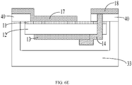
- FIGS. 6A to 6E are process diagrams of a method of manufacturing a monocrystalline film bulk acoustic wave resonator according to another exemplary embodiment of the present disclosure. Referring to FIGS. 6A to 6E , a processing flow of the monocrystalline piezoelectric film bulk acoustic wave resonator is illustrated below.
- a monocrystalline piezoelectric layer and a bottom electrode are formed, as shown in FIG. 6A .
- a monocrystalline seed layer 11 is firstly grown epitaxially on a substrate 50.
- the monocrystalline seed layer may be grown by an epitaxial growth method, such as MOCVD (Metal Organic Chemical Vapor Deposition), MBE (Molecular Beam Epitaxy), CBE (Chemical Molecular Beam Epitaxy), and LPE (Liquid Phase Epitaxy).
- MOCVD Metal Organic Chemical Vapor Deposition
- MBE Molecular Beam Epitaxy
- CBE Chemical Molecular Beam Epitaxy
- LPE Liquid Phase Epitaxy
- a monocrystalline seed layer is provided to promote growth of the monocrystalline piezoelectric layer on the substrate.
- the material of the seed layer may be different from that of the piezoelectric layer 11.
- the seed layer can be used as a barrier layer of the etching process to prevent the piezoelectric layer from being etched in a subsequent process. Further, the monocrystalline seed layer can facilitate the piezoelectric layer to have a good crystal orientation during the epitaxial growth process.
- a monocrystalline piezoelectric layer 12 is then epitaxially grown. After that, a bottom electrode layer 13 is deposited on the monocrystalline piezoelectric layer by a film deposition process, such as CVD (Chemical Vapor Deposition), PVD (Physical Vapor Deposition), PECVD (Plasma Enhanced Chemical Vapor Deposition), evaporation, and sputtering.
- a bottom electrode connection layer is formed, as shown in FIG. 6B . Redundant parts of the monocrystalline piezoelectric material and the seed layer are etched away by photolithography and etching processes, and two sides of the substrate 50 are exposed. It is necessary to form a through hole for forming a bottom electrode connection layer 14 in the monocrystalline seed layer and the substrate. Referring to FIG. 6B , the through hole passes through the monocrystalline seed layer 11 and extends into the substrate 50. The electrode connection layer 14 is then formed to be connected with the bottom electrode 13 through a film deposition process.
- a substrate 33 is attached to the substrate 33.
- a direct bonding technology such as Si-Si bonding, may be adopted between the substrates 33 and 50, or an auxiliary layer may be provided to improve the bonding strength or stick the substrates 33 and 50 with each other.
- An air gap 13 is formed between the substrate 33 and the bottom electrode 13. The air gap 13 functions to confine the sound waves in the resonator. Since the acoustic impedance of air is nearly zero and does not match the acoustic impedance in the resonator, the sound waves can be reflected back into the effective region of the resonator and the Q factor of the resonator can be improved.
- the substrate 50 is then removed, and an insertion layer 40 is formed through which the through hole passes as shown in the figure.
- the structure in FIG. 6C is then turned upside down such that the substrate faces upwards.
- the substrate 50 is thinned by mechanical grinding, and a part of the substrate is then completely removed by etching to form the insertion layer structure 40.
- the insertion layer can increase the mechanical strength and stability of the monocrystalline film resonator, which can make it is used in complex environment. Further, when the material of the insertion layer is the same as that of the substrate, the substrate can be better bonded to the insertion layer, and the sealing performance can be improved. Meanwhile, damage to the monocrystalline piezoelectric layer 12 at the bottom can be prevented due to the seed layer 11 during the etching process of removing the substrate.
- top electrode 17 and the pin layer 18 of the bottom electrode are formed.
- An electrode film is firstly deposited, and the top electrode 17 and the pin layer 18 of the bottom electrode are then formed by photolithography and etching processes. Referring to FIG. 6E , the pin layer 18 is electrically connected to the through hole or the electrode connection layer 14 of the bottom electrode.
- the material of the monocrystalline piezoelectric layer may be monocrystalline aluminum nitride, monocrystalline lithium niobate, monocrystalline lead zirconate titanate, monocrystalline potassium niobate, monocrystalline quartz film, monocrystalline lithium tantalate or the like.
- the material of the top electrode may be following metals or alloys thereof, such as gold, tungsten, molybdenum, platinum, ruthenium, iridium, germanium, copper, titanium, titanium tungsten, aluminum, chromium, and arsenic doped gold.
- the material of the bottom electrode is following metals or alloys thereof, such as gold, tungsten, molybdenum, platinum, ruthenium, iridium, germanium, copper, titanium, titanium tungsten, aluminum, chromium, and arsenic doped gold.
- the materials of the top electrode and the bottom electrode are generally the same, but they may be different.
- the material of the substrate includes Si, quartz, monocrystalline AlN, LiNbO 3 , TaNbO 3 , SiC, GaN, GaAs, PZT, sapphire, diamond or the like.
- a numerical range mentioned in the present disclosure encompass not only end values, but also a median value or other values between the end values, all of which fall within the scope of the present disclosure.
- the bulk acoustic wave resonator according to the present disclosure can be used to form a filter or other semiconductor devices.
Landscapes
- Physics & Mathematics (AREA)
- Acoustics & Sound (AREA)
- Engineering & Computer Science (AREA)
- Manufacturing & Machinery (AREA)
- Piezo-Electric Or Mechanical Vibrators, Or Delay Or Filter Circuits (AREA)
Abstract
Description
- Embodiments of the present disclosure relates to the field of semiconductors, and in particular, to a bulk acoustic wave resonator, a filter having the resonator, a bulk acoustic wave resonator unit, and an electronic apparatus having the resonator or the filter.
- With development of 5G communication technologies, increasingly higher requirements have been posed for communication frequency bands. A traditional radio frequency filter cannot meet requirements for high-frequency communication due to limitation on the structure and performance. A film bulk acoustic resonator (FBAR) used as a new type of MEMS device is adapted to development of wireless communication systems, such that the FBAR technology becomes a research hotspot in the communication field. Compared with the traditional bulk wave acoustic resonator, the FBAR has advantages such as a small volume, light weight, low insertion loss, a wide bandwidth, and a high quality factor, and gradually occupies the market.
- The film bulk acoustic resonator mainly includes a "sandwich" structure composed of electrode-piezoelectric film-electrode, i.e., the piezoelectric film is sandwiched between the two metal electrodes. When a sinusoidal signal is input between the two electrodes, the FBAR converts an input electrical signal into a mechanical resonance through an inverse piezoelectric effect, and then converts the mechanical resonance into an electrical signal output through a piezoelectric effect. The film bulk acoustic resonator mainly utilizes a longitudinal piezoelectric coefficient (d33) of the piezoelectric film to generate the piezoelectric effect, and thus mainly operates in a thickness extensional mode in a thickness direction. The conventional structure is shown in
FIG. 1A , in which a substrate is indicated by 01, a cavity is indicated by 02, a bottom electrode is indicated by 03 and spans both sides of the cavity, a piezoelectric layer is indicated by 04, and a top electrode is indicated by 05. - So far most of the piezoelectric films used in the traditional film bulk acoustic resonators are polycrystalline nitride films prepared by physical or chemical deposition techniques such as magnetron sputtering, which have poor piezoelectric property (mainly indicated by a low electromechanical coupling coefficient of the resonator), a high defect density (mainly indicated by a low quality factor of the resonator), and poor heat dissipation (mainly indicated by a low power capacity of the resonator). Moreover, etched
inclined end faces 06 are formed at both ends of the bottom electrode of the resonator, as shown inFIG. 1 . Since the etched inclined end face has a generally rough surface, defects in the piezoelectric layer deposited on the inclined end faces at the both ends of the bottom electrode may be further increased as shown in a region d inFIG. 1 . These defects may lead to acoustic loss, thereby reducing a Q-factor of the resonator. Moreover, such the resonator cannot meet technical indexes such as lower insertion loss and larger bandwidth required in future mobile communication technologies. - In order to alleviate or solve at least one aspect of above problems in the related art, the present disclosure is provided.
- According to an aspect of embodiments of the present disclosure, there is provided a bulk acoustic wave resonator that includes a substrate, an acoustic mirror, a bottom electrode connected to a bottom electrode pin, a top electrode connected to a top electrode pin, and a piezoelectric layer provided between the bottom electrode and the top electrode. The piezoelectric layer is a monocrystalline piezoelectric film layer. The acoustic mirror, the bottom electrode, the top electrode and the piezoelectric layer overlap with each other in a thickness direction of the resonator to form an overlapping region, and the overlapping region is an effective region of the resonator.
- Optionally, a non-pin end of the top electrode and a non-pin end of the bottom electrode are both spaced apart from an edge of the acoustic mirror in a projection of the resonator in a thickness direction.
- Optionally, the acoustic mirror is an acoustic mirror cavity arranged at an upper side of the substrate and is a blind hole cavity.
- An embodiment of the present disclosure further relates to a bulk acoustic wave resonator unit, which includes the bulk acoustic wave resonator described above and a packaging substrate. The packaging substrate is provided with a circuit device that is electrically connected to the top electrode and the bottom electrode of the resonator, respectively.
- The present disclosure also relates to a method of manufacturing a monocrystalline film bulk acoustic wave resonator. The monocrystalline film bulk acoustic wave resonator includes a substrate, an acoustic mirror, a bottom electrode connected to a bottom electrode pin, a top electrode connected to a top electrode pin, and a monocrystalline piezoelectric film layer provided between the bottom electrode and the top electrode. The method includes: forming the top electrode in such a manner that a non-pin end of the top electrode is spaced apart from an edge of the acoustic mirror in a projection of the resonator in a thickness direction; and forming the bottom electrode in such a manner that a non-pin end of the bottom electrode is spaced apart from the edge of the acoustic mirror in the projection of the resonator in the thickness direction.
- An embodiment of the present disclosure also relates to a filter, which includes the above monocrystalline film bulk acoustic wave resonator, the above monocrystalline film bulk acoustic wave resonator unit, or the monocrystalline film bulk acoustic wave resonator manufactured by the method described above.
- An embodiment of the present disclosure also relates to an electronic apparatus including the above filter, the above resonator, or the above resonator unit.
- The following description and drawings can facilitate to understand these and other features and advantages in various embodiments disclosed in the present disclosure. The same reference signs in the drawings always indicate the same components.
-
FIG. 1A is a schematic sectional view of a conventional bulk acoustic wave resonator. -
FIG. 1B is a schematic top view of a monocrystalline film bulk acoustic wave resonator according to an exemplary embodiment of the present disclosure. -
FIG. 1C is a partial sectional schematic view along A-A inFIG. 1B according to an exemplary embodiment of the present disclosure. -
FIG. 2 is a schematic sectional view of a monocrystalline film bulk acoustic wave resonator according to another exemplary embodiment of the present disclosure. -
FIG. 3 is a schematic sectional view of a monocrystalline film bulk acoustic wave resonator according to an exemplary embodiment of the present disclosure. -
FIG. 4 is a schematic sectional view of a monocrystalline film bulk acoustic wave resonator according to another exemplary embodiment of the present disclosure. -
FIGS. 5A to 5D are process diagrams of a method of manufacturing a monocrystalline film bulk acoustic wave resonator according to an exemplary embodiment of the present disclosure. -
FIGS. 6A to 6E are process diagrams of a method of manufacturing a monocrystalline film bulk acoustic wave resonator according to an exemplary embodiment of the present disclosure. - The technical solutions of the present disclosure will be further described in detail below through embodiments and in conjunction with the drawings. In the specification, the same or similar reference signs refer to the same or similar components. The following description of the embodiments of the present disclosure with reference to the drawings is intended to explain the general inventive concept of the present disclosure, and should not be construed as limitation to the present disclosure.
-
FIG. 1B is a top view of a monocrystalline piezoelectric film bulk acoustic wave resonator according to an exemplary embodiment of the present disclosure. Thereference sign 16 denotes an air gap or cavity of the monocrystalline film resonator. Thereference sign 13 denotes a bottom electrode of the monocrystalline film resonator above the air gap. Thereference sign 12 denotes a monocrystalline piezoelectric film layer of the resonator. Thereference sign 17 denotes a top electrode of the monocrystalline film resonator above the monocrystalline piezoelectric layer. Thereference sign 19a denotes an electrode connection structure on the top electrode. Thereference sign 19b denotes an electrode connection structure on the bottom electrode. InFIG. 1B , it is different from the conventional structure shown inFIG. 1A in that the bottom electrode of the monocrystalline film resonator is located in the cavity in a vertical direction. In the conventional structure, the bottom electrode is located above the cavity in the vertical direction. -
FIG. 1C is a schematic partial sectional view along A-A inFIG. 1B . Thereference sign 15 denotes a substrate, thereference sign 16 denotes an air gap or cavity, thereference sign 13 denotes a bottom electrode, and thereference sign 12 denotes a monocrystalline piezoelectric film layer. A surface of the monocrystalline piezoelectric film layer may or may not be provided with a seed layer. Thereference sign 14 denotes an electrode connection structure of the bottom electrode, thereference sign 17 denotes a top electrode, and thereference sign 18 denotes a bottom electrode pin layer located on an upper surface of the monocrystalline piezoelectric layer. A region where the bottom electrode, the monocrystalline piezoelectric film layer and the top electrode overlap with each other in a thickness direction of the resonator is an effective region of the monocrystalline film resonator, that is, a region indicated by D inFIG. 1C . - In addition, a cavity structure in the related art is generally a through hole passing through the substrate, but the deep etched through hole has disadvantages, such as poor control precision of a cavity shape and dimension, a complex process, complicated electrode connection, and a requirement for an additional packaging process to cover the through hole. In an embodiment of the present disclosure, the
acoustic mirror cavity 16 is a blind hole, and in other words, the acoustic mirror cavity is sealed from below. In this way, a process flow is simplified, the cost is reduced, control precision of the shape and dimension is improved, the electrode connection is more reliable, and an additional through-hole packaging process is unnecessary. - In the embodiment shown in
FIG. 1C , since parts of the top electrode and the bottom electrode in the effective region are both located within the cavity in the vertical direction. In other words, a non-pin end of the top electrode and a non-pin end of the bottom electrode are both spaced apart from an edge of the acoustic mirror in a projection of the monocrystalline film resonator in the thickness direction. This can avoid influence of secondary resonance and spurs generated by the overlapping portion of the top electrode and the bottom electrode in the vertical direction at an edge portion outside the effective region of the monocrystalline film resonator, to effectively improve a Q value of the monocrystalline film resonator. - A material of the piezoelectric layer is a monocrystalline piezoelectric film material, such that the defects of the traditional piezoelectric film material can be compensated, and properties of the resonator, such as an electromechanical coupling coefficient Kt2, a quality factor Q value, and a power capacity, can be greatly improved. Moreover, properties of a filter formed by the monocrystalline piezoelectric film resonator of a monocrystalline piezoelectric film material, such as insertion loss and a suppression ratio of adjacent frequency bands, are also greatly improved.
-
FIG. 2 is a sectional view of a monocrystalline film bulk acoustic wave resonator according to another embodiment of the present disclosure. A structure of the monocrystalline film resonator shown inFIG. 2 is similar to that of the embodiment shown inFIG. 1C , except that a frame structure, i.e., abulge structure 20 and arecess structure 21, is provided at edges of thetop electrode 17 and thebottom electrode 13. The frame structure has a first acoustic impedance, and an effective region D of the monocrystalline film resonator has a second acoustic impedance. The transmission of sound waves is discontinuous at a boundary due to mismatch of the first acoustic impedance and the second acoustic impedance in the frame structure. Accordingly, a part of sound energy at the boundary is coupled and reflected into an effective excitation region, and is converted into a piston acoustic mode perpendicular to a surface of the piezoelectric layer, thereby improving the Q factor of the resonator. - In the embodiments shown in
FIGS. 1C and 2 , the acoustic mirror is a cavity. However, the present disclosure is not limited thereto, and other forms such as a Bragg reflection layer may be adopted. - When the acoustic mirror is a cavity as shown in
FIGS. 1C and 2 , in an embodiment of the present disclosure, the cavity is located between the substrate and a sandwich structure of the monocrystalline film resonator and the bottom electrode is located in the cavity. -
FIG. 3 is a schematic sectional view of a monocrystalline film bulk acoustic wave resonator unit according to an exemplary embodiment of the present disclosure, in which a packaging structure of the monocrystalline film bulk acoustic wave resonator is shown. The monocrystalline film resonator unit inFIG. 3 is different from the monocrystalline film resonator inFIG. 1C in that a packaging structure is provided above the monocrystalline film resonator and is formed by abonding layer 30, connectingpillars 31,solder balls 32, and apackaging substrate 33. The monocrystalline film resonator is isolated from external environment by the packaging structure, and external environmental pollutants, such as external gas, steam, fluid and/or particles, can be prevented from entering an internal space or volume. - As shown in
FIG. 3 , thebottom electrode 13 is located in thecavity 15 in an embodiment. -
FIG. 4 is a schematic sectional view of a monocrystalline film bulk acoustic wave resonator unit according to another exemplary embodiment of the present disclosure, in which a packaging structure of the monocrystalline film bulk acoustic wave resonator is shown. The monocrystalline film resonator unit inFIG. 4 is similar to the monocrystalline film resonator unit inFIG. 3 , except that aninsertion layer 40 is provided on asubstrate 15 and is made of a material same as or different from that of thesubstrate 15. The insertion layer is provided to increase mechanical strength and stability of the monocrystalline film resonator, so that the monocrystalline film resonator can be applied in complex environment. Further, when the material of the insertion layer is the same as that of the substrate, the substrate is better able to be bonded to the insertion layer, to improve the sealing performance. - As shown in
FIG. 4 , thebottom electrode 13 and thepiezoelectric layer 12 are both located in thecavity 16 in an embodiment. - As shown in
FIGS. 3 and 4 , in the monocrystalline film bulk acoustic wave resonator unit according to the present disclosure, the bottom electrode and the monocrystalline piezoelectric layer of the conventional structure are both located in the cavity in the vertical direction, but the bottom electrode and the piezoelectric layer are both located above the cavity in the vertical direction. In other words, the non-pin end of the top electrode and the non-pin end of the bottom electrode are both spaced apart from the edge of the acoustic mirror in the projection of the monocrystalline film resonator in the thickness direction. In this way, generation of spurs in the monocrystalline film resonator can be further avoided, the sound waves can be limited in the effective region of the monocrystalline film resonator, and the Q value of the monocrystalline film resonator can be improved. - As shown in
FIGS. 1C, 2 and3 , in an embodiment of the present disclosure, thebottom electrode pin 14 passes through the monocrystallinepiezoelectric layer 12 to be connected to thebottom electrode 13, and thebottom electrode pin 14 and thebottom electrode 13 are connected to each other in the same layer in the acoustic mirror cavity. - As shown in
FIG. 4 , in an embodiment of the present disclosure, thebottom electrode pin 14 passes through the monocrystallinepiezoelectric layer 12 to be connected to thebottom electrode 13, but thebottom electrode pin 14 and thebottom electrode 13 are stacked and connected with each other in the acoustic mirror cavity. - As shown in
FIGS. 1C, 2 and3 , in an embodiment of the present disclosure, aportion 18 of thebottom electrode pin 14 located at an upper side of the monocrystallinepiezoelectric layer 12 is arranged in the same layer as thetop electrode 17. - As shown in
FIG. 4 , in an embodiment of the present disclosure, the resonator further includes theinsertion layer 40 between the monocrystalline piezoelectric layer and the bottom electrode pin located at the upper side of the monocrystalline piezoelectric layer and between the monocrystalline piezoelectric layer and the top electrode located at the upper side of the monocrystalline piezoelectric layer. Accordingly, as shown inFIG. 4 , a portion of the bottom electrode pin located at the upper side of the monocrystalline piezoelectric layer is arranged in the same layer as the top electrode pin. - The monocrystalline piezoelectric film bulk acoustic wave resonator has a relatively high electromechanical coupling coefficient and a relatively high Q value, and a part of properties of the monocrystalline piezoelectric film bulk acoustic wave resonator is superior to those of the conventional bulk acoustic resonator formed by a piezoelectric film material. However, the monocrystalline piezoelectric film cannot be grown by the simple physical or chemical deposition, so that the resonator structure with the monocrystalline piezoelectric film and the manufacturing method thereof are completely different from the resonator with the polycrystalline piezoelectric film. This means that the resonator structure and processing method are required to be innovated. According to the present disclosure, the traditional FBAR structure and its manufacturing method are changed in a way that the piezoelectric layer of the resonator is made of a monocrystalline piezoelectric material, which can greatly improve the electromechanical coupling coefficient of the resonator and reduce the insertion loss of the filter.
-
FIGS. 5A to 5D are process diagrams of a method of manufacturing a monocrystalline film bulk acoustic wave resonator according to an exemplary embodiment of the present disclosure. Referring toFIGS. 5A to 5D , a processing flow of the monocrystalline piezoelectric film bulk acoustic wave resonator is illustrated below. - Firstly, a monocrystalline piezoelectric layer and a bottom electrode are formed, as shown in
FIG. 5A . Amonocrystalline piezoelectric layer 12 is firstly epitaxially grown on asubstrate 50. The monocrystallinepiezoelectric layer 12 may be grown by an epitaxial growth method, such as MOCVD (Metal Organic Chemical Vapor Deposition), MBE (Molecular Beam Epitaxy), CBE (Chemical Molecular Beam Epitaxy), and LPE (Liquid Phase Epitaxy). In an embodiment, a monocrystalline seed layer is formed. Then, abottom electrode layer 13 is deposited on the monocrystalline piezoelectric layer by a film deposition process, such as CVD (Chemical Vapor Deposition), PVD (Physical Vapor Deposition), PECVD (Plasma Enhanced Chemical Vapor Deposition), evaporation, and sputtering. - After that, a bottom electrode connection layer is formed, as shown in
FIG. 5B . A through hole is formed in the monocrystallinepiezoelectric layer 12 by photolithography and etching, and anelectrode connection layer 14 is formed to be connected with thebottom electrode 13 by a thin film deposition process. - Thereafter, bonding is performed as shown in
FIG. 5C . Asubstrate 33 is attached to the monocrystallinepiezoelectric layer 12 by bonding, and an auxiliary layer may be provided between thesubstrate 33 and the monocrystallinepiezoelectric layer 12 to improve the bonding strength or stick thesubstrate 33 and the monocrystallinepiezoelectric layer 12 with each other. Anair gap 13 is formed between the substrate and thebottom electrode 13. Theair gap 13 is functions to confine the sound waves in the resonator. Since the acoustic impedance of air is nearly zero and does not match the acoustic impedance in the resonator, the sound waves can be reflected back into the effective region of the resonator and the Q factor of the resonator can be improved. - Finally, as shown in
FIG. 5D , thesubstrate 50 is removed to form atop electrode 17 and apin layer 18 of the bottom electrode. The structure inFIG. 5C is then turned upside down to make the substrate facing upwards. Thesubstrate 50 is thinned by mechanical grinding, and the remaining part of the substrate is then completely removed by etching. After that, a thin film is deposited by photolithography and etching processes to form thetop electrode 17 and thepin layer 18 of the bottom electrode. The pin layer is electrically connected to the bottomelectrode connection layer 14. -
FIGS. 6A to 6E are process diagrams of a method of manufacturing a monocrystalline film bulk acoustic wave resonator according to another exemplary embodiment of the present disclosure. Referring toFIGS. 6A to 6E , a processing flow of the monocrystalline piezoelectric film bulk acoustic wave resonator is illustrated below. - Firstly, a monocrystalline piezoelectric layer and a bottom electrode are formed, as shown in
FIG. 6A . Amonocrystalline seed layer 11 is firstly grown epitaxially on asubstrate 50. The monocrystalline seed layer may be grown by an epitaxial growth method, such as MOCVD (Metal Organic Chemical Vapor Deposition), MBE (Molecular Beam Epitaxy), CBE (Chemical Molecular Beam Epitaxy), and LPE (Liquid Phase Epitaxy). A monocrystalline seed layer is provided to promote growth of the monocrystalline piezoelectric layer on the substrate. The material of the seed layer may be different from that of thepiezoelectric layer 11. When the material of the seed layer is different from that of the piezoelectric layer, the seed layer can be used as a barrier layer of the etching process to prevent the piezoelectric layer from being etched in a subsequent process. Further, the monocrystalline seed layer can facilitate the piezoelectric layer to have a good crystal orientation during the epitaxial growth process. Amonocrystalline piezoelectric layer 12 is then epitaxially grown. After that, abottom electrode layer 13 is deposited on the monocrystalline piezoelectric layer by a film deposition process, such as CVD (Chemical Vapor Deposition), PVD (Physical Vapor Deposition), PECVD (Plasma Enhanced Chemical Vapor Deposition), evaporation, and sputtering. - After that, a bottom electrode connection layer is formed, as shown in
FIG. 6B . Redundant parts of the monocrystalline piezoelectric material and the seed layer are etched away by photolithography and etching processes, and two sides of thesubstrate 50 are exposed. It is necessary to form a through hole for forming a bottomelectrode connection layer 14 in the monocrystalline seed layer and the substrate. Referring toFIG. 6B , the through hole passes through themonocrystalline seed layer 11 and extends into thesubstrate 50. Theelectrode connection layer 14 is then formed to be connected with thebottom electrode 13 through a film deposition process. - Thereafter, bonding is performed, as shown in
FIG. 6C . Asubstrate 33 is attached to thesubstrate 33. A direct bonding technology, such as Si-Si bonding, may be adopted between thesubstrates substrates air gap 13 is formed between thesubstrate 33 and thebottom electrode 13. Theair gap 13 functions to confine the sound waves in the resonator. Since the acoustic impedance of air is nearly zero and does not match the acoustic impedance in the resonator, the sound waves can be reflected back into the effective region of the resonator and the Q factor of the resonator can be improved. - Thereafter, the
substrate 50 is then removed, and aninsertion layer 40 is formed through which the through hole passes as shown in the figure. The structure inFIG. 6C is then turned upside down such that the substrate faces upwards. Thesubstrate 50 is thinned by mechanical grinding, and a part of the substrate is then completely removed by etching to form theinsertion layer structure 40. The insertion layer can increase the mechanical strength and stability of the monocrystalline film resonator, which can make it is used in complex environment. Further, when the material of the insertion layer is the same as that of the substrate, the substrate can be better bonded to the insertion layer, and the sealing performance can be improved. Meanwhile, damage to the monocrystallinepiezoelectric layer 12 at the bottom can be prevented due to theseed layer 11 during the etching process of removing the substrate. - Finally, the
top electrode 17 and thepin layer 18 of the bottom electrode are formed. An electrode film is firstly deposited, and thetop electrode 17 and thepin layer 18 of the bottom electrode are then formed by photolithography and etching processes. Referring toFIG. 6E , thepin layer 18 is electrically connected to the through hole or theelectrode connection layer 14 of the bottom electrode. - In the present disclosure, the material of the monocrystalline piezoelectric layer may be monocrystalline aluminum nitride, monocrystalline lithium niobate, monocrystalline lead zirconate titanate, monocrystalline potassium niobate, monocrystalline quartz film, monocrystalline lithium tantalate or the like.
- The material of the top electrode may be following metals or alloys thereof, such as gold, tungsten, molybdenum, platinum, ruthenium, iridium, germanium, copper, titanium, titanium tungsten, aluminum, chromium, and arsenic doped gold. Similarly, the material of the bottom electrode is following metals or alloys thereof, such as gold, tungsten, molybdenum, platinum, ruthenium, iridium, germanium, copper, titanium, titanium tungsten, aluminum, chromium, and arsenic doped gold. The materials of the top electrode and the bottom electrode are generally the same, but they may be different.
- The material of the substrate includes Si, quartz, monocrystalline AlN, LiNbO3, TaNbO3, SiC, GaN, GaAs, PZT, sapphire, diamond or the like.
- A numerical range mentioned in the present disclosure encompass not only end values, but also a median value or other values between the end values, all of which fall within the scope of the present disclosure.
- As can be understood by those skilled in the art, the bulk acoustic wave resonator according to the present disclosure can be used to form a filter or other semiconductor devices.
- In view of the above, the present disclosure provides following technical solutions.
- 1. A bulk acoustic wave resonator includes:
- a substrate;
- an acoustic mirror;
- a bottom electrode connected to a bottom electrode pin;
- a top electrode connected to a top electrode pin; and
- a piezoelectric layer provided between the bottom electrode and the top electrode,
- wherein the piezoelectric layer is a monocrystalline piezoelectric film layer; and
- wherein the acoustic mirror, the bottom electrode, the top electrode and the piezoelectric layer overlap with each other in a thickness direction of the resonator to form an overlapping region, and the overlapping region is an effective region of the resonator.
- 2. The resonator according to 1, wherein
a non-pin end of the top electrode and a non-pin end of the bottom electrode are both spaced apart from an edge of the acoustic mirror in a projection of the resonator in the thickness direction. - 3. The resonator according to 1 or 2, wherein
the acoustic mirror is an acoustic mirror cavity arranged at an upper side of the substrate and is a blind hole. - 4. The resonator according to 3, wherein
the bottom electrode is located in the acoustic mirror cavity, or the bottom electrode and the piezoelectric layer are both located in the acoustic mirror cavity. - 5. The resonator according to 4, wherein
the bottom electrode pin passes through a piezoelectric layer through hole of the piezoelectric layer to be connected to the bottom electrode, and a portion of the bottom electrode pin located at an upper side of the piezoelectric layer is arranged in a same layer as the top electrode. - 6. The resonator according to 4, wherein
- the bottom electrode pin passes through a piezoelectric layer through hole of the piezoelectric layer to be connected to the bottom electrode;
- the resonator further includes an insertion layer, and the insertion layer is provided between the piezoelectric layer and the bottom electrode pin located at an upper side of the piezoelectric layer and between the piezoelectric layer and the top electrode located at the upper side of the piezoelectric layer; and
- a portion of the bottom electrode pin located at the upper side of the piezoelectric layer is arranged in a same layer as the top electrode pin.
- 7. The resonator according to 5 or 6, wherein
- the bottom electrode pin is connected with the bottom electrode in the same layer within the acoustic mirror cavity; or
- the bottom electrode pin and the bottom electrode are connected to and stacked with each other in the acoustic mirror cavity.
- 8. The resonator according to 5 or 6, wherein
the piezoelectric layer through hole is located at an inner side of an edge of the acoustic mirror cavity. - 9. The resonator according to 1 or 2, wherein
an acoustic impedance mismatch structure is provided at a lower side of an edge of the bottom electrode. - 10. The resonator according to 9, wherein
the acoustic impedance mismatch structure includes a bulge structure and a recess structure. - 11. The resonator according to 1 or 2, wherein
a material of the monocrystalline piezoelectric layer is monocrystalline aluminum nitride, monocrystalline lithium niobate, monocrystalline lead zirconate titanate, monocrystalline potassium niobate, monocrystalline quartz film, or monocrystalline lithium tantalate. - 12. A bulk acoustic wave resonator unit includes:
- the resonator according to any one of 1 to 11; and
- a packaging substrate provided with a circuit device, the circuit device being electrically connected to the top electrode and the bottom electrode of the resonator, respectively.
- 13. The resonator unit according to 12, wherein
- the bottom electrode pin passes through the piezoelectric layer to be connected to the bottom electrode, and a portion of the bottom electrode pin located at an upper side of the piezoelectric layer is arranged in a same layer as the top electrode pin; and
- the circuit device includes a bonding layer provided at a lower side of the packaging substrate and a conductive through hole passing through the packaging substrate, and the bonding layer is electrically connected with the conductive through hole and a corresponding one of the bottom electrode pin and the top electrode pin.
- 14. A method of manufacturing a monocrystalline film bulk acoustic wave resonator is provided, in which the monocrystalline film bulk acoustic wave resonator includes a substrate, an acoustic mirror, a bottom electrode connected to a bottom electrode pin, a top electrode connected to a top electrode pin, and a monocrystalline piezoelectric film layer provided between the bottom electrode and the top electrode, the method includes:
- forming the top electrode in such a manner that a non-pin end of the top electrode is spaced apart from an edge of the acoustic mirror in a projection of the monocrystalline film resonator in a thickness direction; and
- forming the bottom electrode in such a manner that a non-pin end of the bottom electrode is spaced apart from the edge of the acoustic mirror in the projection of the monocrystalline film resonator in the thickness direction.
- 15. The method according to 14 further includes:
- sequentially forming the monocrystalline piezoelectric film layer and the bottom electrode on the substrate;
- forming a through hole on the monocrystalline piezoelectric film layer, and forming an electrode connection layer of the bottom electrode at one side of the monocrystalline piezoelectric film layer, in such a manner that the electrode connection layer of the bottom electrode is electrically connected to the bottom electrode and includes a portion located in the through hole;
- providing the substrate on the monocrystalline piezoelectric film layer and forming the acoustic mirror in the substrate, the substrate being formed to be hermetically bonded to the monocrystalline piezoelectric film layer;
- removing the substrate located at another side of the monocrystalline piezoelectric film layer; and
- forming the top electrode and a pin layer electrically connected to a part of the electrode connection layer of the bottom electrode in the through hole at the another side of the monocrystalline piezoelectric film layer.
- 16. The method according to 14 further includes:
- sequentially forming the monocrystalline piezoelectric film layer and the bottom electrode on the substrate;
- forming an electrode connection layer of the bottom electrode at one side of the monocrystalline piezoelectric film layer, in such a manner that the electrode connection layer of the bottom electrode is electrically connected to the bottom electrode;
- providing the substrate on the monocrystalline piezoelectric film layer and forming the acoustic mirror in the substrate, the substrate being formed to be hermetically bonded to the monocrystalline piezoelectric film layer;
- removing the substrate located at another side of the monocrystalline piezoelectric film layer; and
- forming the top electrode and a pin layer electrically connected to the electrode connection layer of the bottom electrode at the another side of the monocrystalline piezoelectric film layer.
- 17. The method according to 15, wherein before the sequentially forming the monocrystalline piezoelectric film layer and the bottom electrode on the substrate, the method further includes forming a monocrystalline seed layer on the substrate;
- in the forming the through hole on the monocrystalline piezoelectric film layer, the through hole passes through the monocrystalline seed layer; and
- in the forming the top electrode at the another side of the monocrystalline piezoelectric film layer, the top electrode is formed on the monocrystalline seed layer located at the another side of the monocrystalline piezoelectric film layer.
- 18. The method according to 15, wherein before the sequentially forming the monocrystalline piezoelectric film layer and the bottom electrode on the substrate, the method further includes forming a monocrystalline seed layer on the substrate; and
in the forming the top electrode at the another side of the monocrystalline piezoelectric film layer, the top electrode is formed on the monocrystalline seed layer located at the another side of the monocrystalline piezoelectric film layer. - 19. The method according to 15 or 16, wherein
- in the forming the through hole in the monocrystalline piezoelectric film layer, the through hole passes through the monocrystalline seed layer and extends into the substrate;
- in the removing the substrate located at the another side of the monocrystalline piezoelectric film layer, the substrate is etched, an insertion layer structure is formed, and the insertion layer structure extends to an inner side of the edge of the acoustic mirror in a lateral direction; and
- in the forming the top electrode and the pin layer electrically connected to the electrode connection layer of the bottom electrode at the another side of the monocrystalline piezoelectric film layer, the top electrode covers the insertion layer structure, the pin layer of the bottom electrode covers the insertion layer structure, and the pin layer of the bottom electrode is electrically connected to the through hole.
- 20. The method according to any one of 14 to 19, wherein
the acoustic mirror is an acoustic mirror cavity, the acoustic mirror cavity is formed between the substrate and the monocrystalline piezoelectric film layer, and the acoustic mirror cavity is a blind hole cavity. - 21. A filter includes the bulk acoustic wave resonator according to any one of 1 to 11, the bulk acoustic wave resonator unit according to 12 or 13, or a monocrystalline film bulk acoustic wave resonator manufactured by the method according to any one of 14 to 20.
- 22. An electronic apparatus includes the filter according to 21, the bulk acoustic wave resonator according to any one of 1 to 11, the bulk acoustic wave resonator unit according to 12 or 13, or a monocrystalline film bulk acoustic wave resonator manufactured by the method according to any one of 14 to 20.
- Although the embodiments of the present disclosure have been shown and described, it should be understood for those skilled in the art that modifications may be made to these embodiments without departing from the principle and spirit of the present disclosure, and the scope thereof is defined by the appended claims and their equivalents.
Claims (22)
- A bulk acoustic wave resonator, comprising:a substrate;an acoustic mirror;a bottom electrode connected to a bottom electrode pin;a top electrode connected to a top electrode pin; anda piezoelectric layer provided between the bottom electrode and the top electrode,wherein the piezoelectric layer is a monocrystalline piezoelectric film layer; andwherein the acoustic mirror, the bottom electrode, the top electrode and the monocrystalline piezoelectric film layer overlap with each other in a thickness direction of the resonator to form an overlapping region, and the overlapping region is an effective region of the resonator.
- The resonator according to claim 1, wherein a non-pin end of the top electrode and a non-pin end of the bottom electrode are both spaced apart from an edge of the acoustic mirror in a projection of the resonator in the thickness direction.
- The resonator according to claim 1 or 2, wherein the acoustic mirror is an acoustic mirror cavity arranged at an upper side of the substrate and is a blind hole cavity.
- The resonator according to claim 3, wherein the bottom electrode is located in the acoustic mirror cavity, or the bottom electrode and the piezoelectric layer are both located in the acoustic mirror cavity.
- The resonator according to claim 4, wherein the bottom electrode pin passes through a piezoelectric layer through hole of the piezoelectric layer to be connected to the bottom electrode, and a portion of the bottom electrode pin located at an upper side of the piezoelectric layer is arranged in a same layer as the top electrode.
- The resonator according to claim 4, wherein the bottom electrode pin passes through a piezoelectric layer through hole of the piezoelectric layer to be connected to the bottom electrode;the resonator further comprises an insertion layer, and the insertion layer is provided between the piezoelectric layer and the bottom electrode pin located at an upper side of the piezoelectric layer and between the piezoelectric layer and the top electrode located at the upper side of the piezoelectric layer; anda portion of the bottom electrode pin located at the upper side of the piezoelectric layer is arranged in a same layer as the top electrode pin.
- The resonator according to claim 5 or 6, wherein the bottom electrode pin is connected with the bottom electrode in the same layer within the acoustic mirror cavity; or
the bottom electrode pin and the bottom electrode are connected to and stacked with each other within the acoustic mirror cavity. - The resonator according to claim 5 or 6, wherein the piezoelectric layer through hole is located at an inner side of an edge of the acoustic mirror cavity.
- The resonator according to claim 1 or 2, further comprising:
an acoustic impedance mismatch structure provided at a lower side of an edge of the bottom electrode. - The resonator according to claim 9, wherein the acoustic impedance mismatch structure comprises a bulge structure and a recess structure.
- The resonator according to claim 1 or 2, wherein a material of the monocrystalline piezoelectric layer is monocrystalline aluminum nitride, monocrystalline lithium niobate, monocrystalline lead zirconate titanate, monocrystalline potassium niobate, monocrystalline quartz film, or monocrystalline lithium tantalate.
- A bulk acoustic wave resonator unit, comprising:the resonator according to any one of claims 1 to 11; anda packaging substrate provided with a circuit device, the circuit device being electrically connected to the top electrode and the bottom electrode of the resonator, respectively.
- The resonator unit according to claim 12, wherein the bottom electrode pin passes through the piezoelectric layer to be connected to the bottom electrode, and a portion of the bottom electrode pin located at an upper side of the piezoelectric layer is arranged in a same layer as the top electrode pin; and
the circuit device comprises a bonding layer provided at a lower side of the packaging substrate and a conductive through hole passing through the packaging substrate, and the bonding layer is electrically connected with the conductive through hole and a corresponding one of the bottom electrode pin and the top electrode pin. - A method of manufacturing a monocrystalline film bulk acoustic wave resonator, wherein the monocrystalline film bulk acoustic wave resonator comprises a substrate, an acoustic mirror, a bottom electrode connected to a bottom electrode pin, a top electrode connected to a top electrode pin, and a monocrystalline piezoelectric film layer provided between the bottom electrode and the top electrode, the method comprises:forming the top electrode in such a manner that a non-pin end of the top electrode is spaced apart from an edge of the acoustic mirror in a projection of the monocrystalline film resonator in a thickness direction; andforming the bottom electrode in such a manner that a non-pin end of the bottom electrode is spaced apart from the edge of the acoustic mirror in the projection of the monocrystalline film resonator in the thickness direction.
- The method according to claim 14, further comprising:sequentially forming the monocrystalline piezoelectric film layer and the bottom electrode on the substrate;forming a through hole on the monocrystalline piezoelectric film layer, and forming an bottom electrode connection layer at one side of the monocrystalline piezoelectric film layer, in such a manner that the bottom electrode connection layer is electrically connected to the bottom electrode and comprises a portion located in the through hole;providing the substrate on the monocrystalline piezoelectric film layer and forming the acoustic mirror in the substrate, the substrate being formed to be hermetically bonded to the monocrystalline piezoelectric film layer;removing the substrate located at another side of the monocrystalline piezoelectric film layer; andforming, at the another side of the monocrystalline piezoelectric film layer, the top electrode and a pin layer electrically connected to a part of the bottom electrode connection layer in the through hole.
- The method according to claim 14, further comprising:sequentially forming the monocrystalline piezoelectric film layer and the bottom electrode on the substrate;forming a bottom electrode connection layer at one side of the monocrystalline piezoelectric film layer, in such a manner that the bottom electrode connection layer is electrically connected to the bottom electrode;providing the substrate on the monocrystalline piezoelectric film layer and forming the acoustic mirror in the substrate, the substrate being formed to be hermetically bonded to the monocrystalline piezoelectric film layer;removing the substrate located at another side of the monocrystalline piezoelectric film layer; andforming the top electrode and a pin layer electrically connected to the bottom electrode connection layer at the another side of the monocrystalline piezoelectric film layer.
- The method according to claim 15, wherein before the sequentially forming the monocrystalline piezoelectric film layer and the bottom electrode on the substrate, the method further comprises forming a monocrystalline seed layer on the substrate;in the forming the through hole on the monocrystalline piezoelectric film layer, the through hole passes through the monocrystalline seed layer; andin the forming the top electrode at the another side of the monocrystalline piezoelectric film layer, the top electrode is formed on the monocrystalline seed layer located at the another side of the monocrystalline piezoelectric film layer.
- The method according to claim 15, wherein before the sequentially forming the monocrystalline piezoelectric film layer and the bottom electrode on the substrate, the method further comprises forming a monocrystalline seed layer on the substrate; and
in the forming the top electrode at the another side of the monocrystalline piezoelectric film layer, the top electrode is formed on the monocrystalline seed layer located at the another side of the monocrystalline piezoelectric film layer. - The method according to claim 15 or 16, wherein in the forming the through hole in the monocrystalline piezoelectric film layer, the through hole passes through the monocrystalline seed layer and extends into the substrate;in the removing the substrate located at the another side of the monocrystalline piezoelectric film layer, the substrate is etched, an insertion layer structure is formed, and the insertion layer structure extends to an inner side of the edge of the acoustic mirror in a lateral direction; andin the forming the top electrode and the pin layer electrically connected to the electrode connection layer of the bottom electrode at the another side of the monocrystalline piezoelectric film layer, the top electrode covers the insertion layer structure, the pin layer of the bottom electrode covers the insertion layer structure, and the pin layer of the bottom electrode is electrically connected to the through hole.
- The method according to any one of claims 14 to 19, wherein the acoustic mirror is an acoustic mirror cavity, the acoustic mirror cavity is formed between the substrate and the monocrystalline piezoelectric film layer, and the acoustic mirror cavity is a blind hole cavity.
- A filter, comprising the bulk acoustic wave resonator according to any one of claims 1 to 11, the bulk acoustic wave resonator unit according to claim 12 or 13, or a monocrystalline film bulk acoustic wave resonator manufactured by the method according to any one of claims 14 to 20.
- An electronic apparatus, comprising the filter according to claim 21, the bulk acoustic wave resonator according to any one of claims 1 to 11, the bulk acoustic wave resonator unit according to claim 11 or 13, or a monocrystalline film bulk acoustic wave resonator manufactured by the method according to any one of claims 14 to 20.
Applications Claiming Priority (2)
| Application Number | Priority Date | Filing Date | Title |
|---|---|---|---|
| CN201911241860.3A CN111245397B (en) | 2019-12-06 | 2019-12-06 | Bulk acoustic wave resonator, method of manufacturing the same, bulk acoustic wave resonator unit, filter, and electronic apparatus |
| PCT/CN2020/086564 WO2021109426A1 (en) | 2019-12-06 | 2020-04-24 | Bulk acoustic wave resonator and manufacturing method, bulk acoustic wave resonator unit, filter and electronic device |
Publications (2)
| Publication Number | Publication Date |
|---|---|
| EP4089918A1 true EP4089918A1 (en) | 2022-11-16 |
| EP4089918A4 EP4089918A4 (en) | 2024-07-10 |
Family
ID=70875852
Family Applications (1)
| Application Number | Title | Priority Date | Filing Date |
|---|---|---|---|
| EP20896703.4A Pending EP4089918A4 (en) | 2019-12-06 | 2020-04-24 | VOLUME ACOUSTIC WAVE RESONATOR AND METHOD FOR MANUFACTURING SAME, VOLUME ACOUSTIC WAVE RESONATOR UNIT, FILTER AND ELECTRONIC DEVICE |
Country Status (3)
| Country | Link |
|---|---|
| EP (1) | EP4089918A4 (en) |
| CN (1) | CN111245397B (en) |
| WO (1) | WO2021109426A1 (en) |
Cited By (1)
| Publication number | Priority date | Publication date | Assignee | Title |
|---|---|---|---|---|
| EP4152610A1 (en) * | 2021-08-31 | 2023-03-22 | National Yang Ming Chiao Tung University | Crystal oscillator, and method for making the same |
Families Citing this family (32)
| Publication number | Priority date | Publication date | Assignee | Title |
|---|---|---|---|---|
| CN113872553B (en) * | 2020-06-30 | 2025-10-17 | 诺思(天津)微系统有限责任公司 | Bulk acoustic wave resonator, method of manufacturing the same, filter, and electronic apparatus |
| CN111969974A (en) * | 2020-07-13 | 2020-11-20 | 深圳市汇芯通信技术有限公司 | Bulk acoustic wave filter, manufacturing method thereof and integrated chip |
| CN112383286B (en) * | 2020-08-04 | 2021-09-21 | 诺思(天津)微系统有限责任公司 | Bulk acoustic wave resonator assembly, method of manufacturing the same, filter, and electronic apparatus |
| CN112532195B (en) * | 2020-12-02 | 2021-11-12 | 海宁波恩斯坦生物科技有限公司 | Passive cavity type single crystal film bulk acoustic resonator structure and preparation method thereof |
| CN114744974B (en) * | 2021-01-07 | 2026-01-02 | 诺思(天津)微系统有限责任公司 | Bulk acoustic resonators and their manufacturing methods, filters and electronic equipment |
| CN113285689B (en) * | 2021-03-05 | 2023-01-31 | 天津大学 | Quartz crystal resonator, method for forming same, and electronic device |
| CN113285685B (en) * | 2021-03-05 | 2022-12-09 | 广州乐仪投资有限公司 | Quartz film bulk acoustic resonator, processing method thereof and electronic equipment |
| CN113037245B (en) * | 2021-03-11 | 2023-02-03 | 天津大学 | Quartz resonator based on piezoelectric thin film transduction and electronic equipment |
| WO2022188100A1 (en) * | 2021-03-11 | 2022-09-15 | 天津大学 | Quartz resonator based on piezoelectric thin-film transduction, and electronic device |
| CN113300689B (en) * | 2021-03-29 | 2023-01-31 | 天津大学 | Quartz resonator with reinforced structure, forming method thereof and electronic equipment |
| CN115250107A (en) * | 2021-04-26 | 2022-10-28 | 诺思(天津)微系统有限责任公司 | Bulk acoustic wave resonator and method of making the same, filter and electronic device |
| CN115250102A (en) * | 2021-04-27 | 2022-10-28 | 诺思(天津)微系统有限责任公司 | Bulk acoustic wave resonator, filter, and electronic device having thickened electrodes |
| CN115250104A (en) * | 2021-04-27 | 2022-10-28 | 诺思(天津)微系统有限责任公司 | Bulk acoustic wave resonator, filter, and electronic device |
| CN113824420A (en) * | 2021-08-23 | 2021-12-21 | 杭州电子科技大学 | Preparation method of single crystal thin film bulk acoustic wave resonator with double ring structure electrodes |
| CN113839637A (en) * | 2021-08-26 | 2021-12-24 | 杭州电子科技大学 | Preparation method of single crystal thin film bulk acoustic wave resonator with electrode with ring groove and strip protrusion |
| CN113839638A (en) * | 2021-08-30 | 2021-12-24 | 杭州电子科技大学 | Method for preparing film bulk acoustic resonator with electrodes provided with double-ring and bridge structures |
| CN116073789B (en) * | 2021-11-01 | 2024-08-23 | 南京大学 | Bulk acoustic wave resonator based on double-layer lithium niobate single crystal thin film |
| CN114759897B (en) * | 2022-04-11 | 2023-05-23 | 浙江星曜半导体有限公司 | Film bulk acoustic resonator and preparation method thereof |
| CN116961611A (en) * | 2022-04-20 | 2023-10-27 | 京东方科技集团股份有限公司 | A bulk acoustic wave resonator, a preparation method of a bulk acoustic wave resonator and electronic equipment |
| CN117548315A (en) * | 2022-08-05 | 2024-02-13 | 天津大学 | PMUT structure integrating transistor unit with PMUT unit with cavity |
| CN117548316A (en) * | 2022-08-05 | 2024-02-13 | 天津大学 | PMUT structure in which the supporting layer is a single crystal thin film layer |
| CN117559941A (en) * | 2022-08-05 | 2024-02-13 | 天津大学 | Quartz resonator with electrode lead-out portions on the same side, manufacturing method thereof, and electronic device |
| CN117559947A (en) * | 2022-08-05 | 2024-02-13 | 天津大学 | Quartz resonator whose piezoelectric layer is an inverted platform structure, its manufacturing method, and electronic device |
| CN115225051A (en) * | 2022-09-20 | 2022-10-21 | 深圳新声半导体有限公司 | Resonator structure, method for making resonator structure |
| CN115632630B (en) * | 2022-11-01 | 2026-04-14 | 常州承芯半导体有限公司 | Method for forming a bulk acoustic resonator |
| CN115589212B (en) * | 2022-12-12 | 2023-04-11 | 成都频岢微电子有限公司 | Bulk acoustic wave resonator with thin film package, manufacturing method and filter |
| CN116155223B (en) * | 2022-12-30 | 2026-04-17 | 苏州汉天下电子有限公司 | A method for manufacturing a bulk acoustic resonator and its application |
| CN116683886A (en) * | 2023-07-28 | 2023-09-01 | 深圳新声半导体有限公司 | A kind of filter and preparation method thereof |
| CN117375560B (en) * | 2023-10-09 | 2024-07-16 | 武汉敏声新技术有限公司 | A bulk acoustic wave resonator device and a method for manufacturing the same |
| CN118100840A (en) * | 2024-03-11 | 2024-05-28 | 睿思微系统(烟台)有限公司 | A method for preparing a bulk acoustic wave resonator and a bulk acoustic wave resonator |
| CN119602739B (en) * | 2024-11-27 | 2025-09-09 | 广州市艾佛光通科技有限公司 | Bulk acoustic wave resonator with high electrical property, preparation method and bulk acoustic wave filter |
| CN120934483B (en) * | 2025-10-13 | 2026-01-06 | 广州市艾佛光通科技有限公司 | A high-Q bulk acoustic resonator, filter, duplexer, and their fabrication method |
Family Cites Families (10)
| Publication number | Priority date | Publication date | Assignee | Title |
|---|---|---|---|---|
| JP3949990B2 (en) * | 2002-03-29 | 2007-07-25 | 株式会社東芝 | Voltage controlled oscillator |
| EP1469599B1 (en) * | 2003-04-18 | 2010-11-03 | Samsung Electronics Co., Ltd. | Air gap type FBAR, duplexer using the FBAR, and fabricating methods thereof |
| CN103296992B (en) * | 2013-06-28 | 2016-02-10 | 中国电子科技集团公司第二十六研究所 | Film bulk acoustic resonator structure and manufacturing method thereof |
| CN205792476U (en) * | 2016-05-31 | 2016-12-07 | 中电科技德清华莹电子有限公司 | A kind of FBAR using ultra-thin piezoelectric single crystal to make |
| US10855250B2 (en) * | 2016-07-11 | 2020-12-01 | Akoustis, Inc. | Communication filter for LTE band 41 |
| CN107222181A (en) * | 2016-12-29 | 2017-09-29 | 杭州左蓝微电子技术有限公司 | FBAR based on SOI Substrate and preparation method thereof |
| CN106788306A (en) * | 2017-03-07 | 2017-05-31 | 杭州左蓝微电子技术有限公司 | A kind of FBAR and preparation method thereof |
| CN108667437B (en) * | 2018-04-19 | 2022-04-26 | 中芯集成电路(宁波)有限公司 | Film bulk acoustic resonator, manufacturing method thereof and electronic device |
| CN109889179A (en) * | 2018-12-26 | 2019-06-14 | 天津大学 | Resonators and Ladder Filters |
| CN110492860A (en) * | 2019-08-27 | 2019-11-22 | 南方科技大学 | Thin film bulk acoustic wave resonator and its manufacturing method |
-
2019
- 2019-12-06 CN CN201911241860.3A patent/CN111245397B/en active Active
-
2020
- 2020-04-24 WO PCT/CN2020/086564 patent/WO2021109426A1/en not_active Ceased
- 2020-04-24 EP EP20896703.4A patent/EP4089918A4/en active Pending
Cited By (1)
| Publication number | Priority date | Publication date | Assignee | Title |
|---|---|---|---|---|
| EP4152610A1 (en) * | 2021-08-31 | 2023-03-22 | National Yang Ming Chiao Tung University | Crystal oscillator, and method for making the same |
Also Published As
| Publication number | Publication date |
|---|---|
| WO2021109426A1 (en) | 2021-06-10 |
| CN111245397B (en) | 2024-08-02 |
| CN111245397A (en) | 2020-06-05 |
| EP4089918A4 (en) | 2024-07-10 |
Similar Documents
| Publication | Publication Date | Title |
|---|---|---|
| CN111245397B (en) | Bulk acoustic wave resonator, method of manufacturing the same, bulk acoustic wave resonator unit, filter, and electronic apparatus | |
| CN111245394B (en) | Bulk acoustic wave resonator, filter and electronic device with electrode with void layer and temperature compensation layer | |
| EP4087130A1 (en) | Bulk acoustic resonator with bottom electrode as gap electrode, and filter and electronic device | |
| US11923826B2 (en) | Film bulk acoustic resonator and fabrication method thereof | |
| CN111245393B (en) | Bulk acoustic wave resonator, method of manufacturing the same, filter, and electronic apparatus | |
| JP7081041B2 (en) | Thin-film bulk acoustic wave resonators and their manufacturing methods, filters, and radio frequency communication systems | |
| WO2021077715A1 (en) | Bulk acoustic wave resonator provided with electrodes having gap layer and protruding structure, filter and electronic device | |
| CN111600569B (en) | Bulk acoustic wave resonator, method of manufacturing the same, filter, and electronic apparatus | |
| CN111010099B (en) | Bulk acoustic resonator with concave structure and convex structure, filter and electronic equipment | |
| US20020079986A1 (en) | Bulk acoustic resonator perimeter reflection system | |
| WO2020098481A1 (en) | Bulk acoustic wave resonator having rough surface, filter, and electronic device | |
| CN111010108B (en) | Bulk acoustic wave resonator, filter and electronic device with concave and air wing structure | |
| EP4050795A1 (en) | Bulk acoustic resonator, filter, and electronic device | |
| JP2022507325A (en) | Bulk acoustic wave resonator and its manufacturing method, filter, radio frequency communication system | |
| WO2021189964A1 (en) | Thin film bulk acoustic resonator and manufacturing method therefor | |
| JP2021503229A (en) | Piezoelectric resonator and manufacturing method of piezoelectric resonator | |
| CN112787614A (en) | Thin film lamb wave resonator, filter and manufacturing method thereof | |
| JP2022507306A (en) | Bulk acoustic wave resonator and its manufacturing method, filter, radio frequency communication system | |
| CN112039483B (en) | Film bulk acoustic resonator | |
| CN112311353A (en) | Firmly-arranged bulk acoustic wave resonator and manufacturing method thereof | |
| WO2020098484A1 (en) | Bulk acoustic wave resonator having fracture structure and manufacturing method therefor, filter, and electronic device | |
| JP2022507221A (en) | Bulk acoustic wave resonator and its manufacturing method, filter, radio frequency communication system | |
| CN116961611A (en) | A bulk acoustic wave resonator, a preparation method of a bulk acoustic wave resonator and electronic equipment | |
| US20230216479A1 (en) | Acoustic resonator in transverse excitation shear mode | |
| US20250357910A1 (en) | Resonator and method for forming the same |
Legal Events
| Date | Code | Title | Description |
|---|---|---|---|
| STAA | Information on the status of an ep patent application or granted ep patent |
Free format text: STATUS: THE INTERNATIONAL PUBLICATION HAS BEEN MADE |
|
| PUAI | Public reference made under article 153(3) epc to a published international application that has entered the european phase |
Free format text: ORIGINAL CODE: 0009012 |
|
| STAA | Information on the status of an ep patent application or granted ep patent |
Free format text: STATUS: REQUEST FOR EXAMINATION WAS MADE |
|
| 17P | Request for examination filed |
Effective date: 20220706 |
|
| AK | Designated contracting states |
Kind code of ref document: A1 Designated state(s): AL AT BE BG CH CY CZ DE DK EE ES FI FR GB GR HR HU IE IS IT LI LT LU LV MC MK MT NL NO PL PT RO RS SE SI SK SM TR |
|
| DAV | Request for validation of the european patent (deleted) | ||
| DAX | Request for extension of the european patent (deleted) | ||
| RIC1 | Information provided on ipc code assigned before grant |
Ipc: H03H 9/05 20060101ALN20240313BHEP Ipc: H03H 9/54 20060101ALI20240313BHEP Ipc: H03H 3/02 20060101ALI20240313BHEP Ipc: H03H 9/02 20060101ALI20240313BHEP Ipc: H03H 9/17 20060101AFI20240313BHEP |
|
| A4 | Supplementary search report drawn up and despatched |
Effective date: 20240611 |
|
| RIC1 | Information provided on ipc code assigned before grant |
Ipc: H03H 9/05 20060101ALN20240605BHEP Ipc: H03H 9/54 20060101ALI20240605BHEP Ipc: H03H 3/02 20060101ALI20240605BHEP Ipc: H03H 9/02 20060101ALI20240605BHEP Ipc: H03H 9/17 20060101AFI20240605BHEP |