EP4085299B1 - Optisches system, isolierverglasung, die ein solches optisches system umfasst, verfahren zum herstellen dieser isolierverglasung und verfahren zum schützen eines optischen systems - Google Patents
Optisches system, isolierverglasung, die ein solches optisches system umfasst, verfahren zum herstellen dieser isolierverglasung und verfahren zum schützen eines optischen systems Download PDFInfo
- Publication number
- EP4085299B1 EP4085299B1 EP20851235.0A EP20851235A EP4085299B1 EP 4085299 B1 EP4085299 B1 EP 4085299B1 EP 20851235 A EP20851235 A EP 20851235A EP 4085299 B1 EP4085299 B1 EP 4085299B1
- Authority
- EP
- European Patent Office
- Prior art keywords
- optical system
- protective layer
- layer
- electrochromic stack
- optical element
- Prior art date
- Legal status (The legal status is an assumption and is not a legal conclusion. Google has not performed a legal analysis and makes no representation as to the accuracy of the status listed.)
- Active
Links
Images

Classifications
-
- G—PHYSICS
- G02—OPTICS
- G02F—OPTICAL DEVICES OR ARRANGEMENTS FOR THE CONTROL OF LIGHT BY MODIFICATION OF THE OPTICAL PROPERTIES OF THE MEDIA OF THE ELEMENTS INVOLVED THEREIN; NON-LINEAR OPTICS; FREQUENCY-CHANGING OF LIGHT; OPTICAL LOGIC ELEMENTS; OPTICAL ANALOGUE/DIGITAL CONVERTERS
- G02F1/00—Devices or arrangements for the control of the intensity, colour, phase, polarisation or direction of light arriving from an independent light source, e.g. switching, gating or modulating; Non-linear optics
- G02F1/01—Devices or arrangements for the control of the intensity, colour, phase, polarisation or direction of light arriving from an independent light source, e.g. switching, gating or modulating; Non-linear optics for the control of the intensity, phase, polarisation or colour
- G02F1/15—Devices or arrangements for the control of the intensity, colour, phase, polarisation or direction of light arriving from an independent light source, e.g. switching, gating or modulating; Non-linear optics for the control of the intensity, phase, polarisation or colour based on an electrochromic effect
- G02F1/153—Constructional details
- G02F1/1533—Constructional details structural features not otherwise provided for
-
- B—PERFORMING OPERATIONS; TRANSPORTING
- B29—WORKING OF PLASTICS; WORKING OF SUBSTANCES IN A PLASTIC STATE IN GENERAL
- B29D—PRODUCING PARTICULAR ARTICLES FROM PLASTICS OR FROM SUBSTANCES IN A PLASTIC STATE
- B29D11/00—Producing optical elements, e.g. lenses or prisms
- B29D11/0074—Production of other optical elements not provided for in B29D11/00009- B29D11/0073
-
- B—PERFORMING OPERATIONS; TRANSPORTING
- B32—LAYERED PRODUCTS
- B32B—LAYERED PRODUCTS, i.e. PRODUCTS BUILT-UP OF STRATA OF FLAT OR NON-FLAT, e.g. CELLULAR OR HONEYCOMB, FORM
- B32B17/00—Layered products essentially comprising sheet glass, or glass, slag, or like fibres
- B32B17/06—Layered products essentially comprising sheet glass, or glass, slag, or like fibres comprising glass as the main or only constituent of a layer, next to another layer of a specific material
- B32B17/10—Layered products essentially comprising sheet glass, or glass, slag, or like fibres comprising glass as the main or only constituent of a layer, next to another layer of a specific material of synthetic resin
- B32B17/10005—Layered products essentially comprising sheet glass, or glass, slag, or like fibres comprising glass as the main or only constituent of a layer, next to another layer of a specific material of synthetic resin laminated safety glass or glazing
- B32B17/10009—Layered products essentially comprising sheet glass, or glass, slag, or like fibres comprising glass as the main or only constituent of a layer, next to another layer of a specific material of synthetic resin laminated safety glass or glazing characterized by the number, the constitution or treatment of glass sheets
- B32B17/10036—Layered products essentially comprising sheet glass, or glass, slag, or like fibres comprising glass as the main or only constituent of a layer, next to another layer of a specific material of synthetic resin laminated safety glass or glazing characterized by the number, the constitution or treatment of glass sheets comprising two outer glass sheets
- B32B17/10045—Layered products essentially comprising sheet glass, or glass, slag, or like fibres comprising glass as the main or only constituent of a layer, next to another layer of a specific material of synthetic resin laminated safety glass or glazing characterized by the number, the constitution or treatment of glass sheets comprising two outer glass sheets with at least one intermediate layer consisting of a glass sheet
- B32B17/10055—Layered products essentially comprising sheet glass, or glass, slag, or like fibres comprising glass as the main or only constituent of a layer, next to another layer of a specific material of synthetic resin laminated safety glass or glazing characterized by the number, the constitution or treatment of glass sheets comprising two outer glass sheets with at least one intermediate layer consisting of a glass sheet with at least one intermediate air space
-
- B—PERFORMING OPERATIONS; TRANSPORTING
- B32—LAYERED PRODUCTS
- B32B—LAYERED PRODUCTS, i.e. PRODUCTS BUILT-UP OF STRATA OF FLAT OR NON-FLAT, e.g. CELLULAR OR HONEYCOMB, FORM
- B32B17/00—Layered products essentially comprising sheet glass, or glass, slag, or like fibres
- B32B17/06—Layered products essentially comprising sheet glass, or glass, slag, or like fibres comprising glass as the main or only constituent of a layer, next to another layer of a specific material
- B32B17/10—Layered products essentially comprising sheet glass, or glass, slag, or like fibres comprising glass as the main or only constituent of a layer, next to another layer of a specific material of synthetic resin
- B32B17/10005—Layered products essentially comprising sheet glass, or glass, slag, or like fibres comprising glass as the main or only constituent of a layer, next to another layer of a specific material of synthetic resin laminated safety glass or glazing
- B32B17/10165—Functional features of the laminated safety glass or glazing
- B32B17/10174—Coatings of a metallic or dielectric material on a constituent layer of glass or polymer
- B32B17/10201—Dielectric coatings
- B32B17/10211—Doped dielectric layer, electrically conductive, e.g. SnO2:F
-
- B—PERFORMING OPERATIONS; TRANSPORTING
- B32—LAYERED PRODUCTS
- B32B—LAYERED PRODUCTS, i.e. PRODUCTS BUILT-UP OF STRATA OF FLAT OR NON-FLAT, e.g. CELLULAR OR HONEYCOMB, FORM
- B32B17/00—Layered products essentially comprising sheet glass, or glass, slag, or like fibres
- B32B17/06—Layered products essentially comprising sheet glass, or glass, slag, or like fibres comprising glass as the main or only constituent of a layer, next to another layer of a specific material
- B32B17/10—Layered products essentially comprising sheet glass, or glass, slag, or like fibres comprising glass as the main or only constituent of a layer, next to another layer of a specific material of synthetic resin
- B32B17/10005—Layered products essentially comprising sheet glass, or glass, slag, or like fibres comprising glass as the main or only constituent of a layer, next to another layer of a specific material of synthetic resin laminated safety glass or glazing
- B32B17/10165—Functional features of the laminated safety glass or glazing
- B32B17/10431—Specific parts for the modulation of light incorporated into the laminated safety glass or glazing
- B32B17/10467—Variable transmission
- B32B17/10495—Variable transmission optoelectronic, i.e. optical valve
- B32B17/10513—Electrochromic layer
-
- C—CHEMISTRY; METALLURGY
- C03—GLASS; MINERAL OR SLAG WOOL
- C03B—MANUFACTURE, SHAPING, OR SUPPLEMENTARY PROCESSES
- C03B27/00—Tempering or quenching glass products
-
- C—CHEMISTRY; METALLURGY
- C03—GLASS; MINERAL OR SLAG WOOL
- C03C—CHEMICAL COMPOSITION OF GLASSES, GLAZES OR VITREOUS ENAMELS; SURFACE TREATMENT OF GLASS; SURFACE TREATMENT OF FIBRES OR FILAMENTS MADE FROM GLASS, MINERALS OR SLAGS; JOINING GLASS TO GLASS OR OTHER MATERIALS
- C03C17/00—Surface treatment of glass, not in the form of fibres or filaments, by coating
- C03C17/34—Surface treatment of glass, not in the form of fibres or filaments, by coating with at least two coatings having different compositions
- C03C17/36—Surface treatment of glass, not in the form of fibres or filaments, by coating with at least two coatings having different compositions at least one coating being a metal
- C03C17/3602—Surface treatment of glass, not in the form of fibres or filaments, by coating with at least two coatings having different compositions at least one coating being a metal the metal being present as a layer
- C03C17/3657—Surface treatment of glass, not in the form of fibres or filaments, by coating with at least two coatings having different compositions at least one coating being a metal the metal being present as a layer the multilayer coating having optical properties
-
- C—CHEMISTRY; METALLURGY
- C03—GLASS; MINERAL OR SLAG WOOL
- C03C—CHEMICAL COMPOSITION OF GLASSES, GLAZES OR VITREOUS ENAMELS; SURFACE TREATMENT OF GLASS; SURFACE TREATMENT OF FIBRES OR FILAMENTS MADE FROM GLASS, MINERALS OR SLAGS; JOINING GLASS TO GLASS OR OTHER MATERIALS
- C03C17/00—Surface treatment of glass, not in the form of fibres or filaments, by coating
- C03C17/34—Surface treatment of glass, not in the form of fibres or filaments, by coating with at least two coatings having different compositions
- C03C17/36—Surface treatment of glass, not in the form of fibres or filaments, by coating with at least two coatings having different compositions at least one coating being a metal
- C03C17/3602—Surface treatment of glass, not in the form of fibres or filaments, by coating with at least two coatings having different compositions at least one coating being a metal the metal being present as a layer
- C03C17/3668—Surface treatment of glass, not in the form of fibres or filaments, by coating with at least two coatings having different compositions at least one coating being a metal the metal being present as a layer the multilayer coating having electrical properties
- C03C17/3671—Surface treatment of glass, not in the form of fibres or filaments, by coating with at least two coatings having different compositions at least one coating being a metal the metal being present as a layer the multilayer coating having electrical properties specially adapted for use as electrodes
-
- C—CHEMISTRY; METALLURGY
- C03—GLASS; MINERAL OR SLAG WOOL
- C03C—CHEMICAL COMPOSITION OF GLASSES, GLAZES OR VITREOUS ENAMELS; SURFACE TREATMENT OF GLASS; SURFACE TREATMENT OF FIBRES OR FILAMENTS MADE FROM GLASS, MINERALS OR SLAGS; JOINING GLASS TO GLASS OR OTHER MATERIALS
- C03C17/00—Surface treatment of glass, not in the form of fibres or filaments, by coating
- C03C17/34—Surface treatment of glass, not in the form of fibres or filaments, by coating with at least two coatings having different compositions
- C03C17/36—Surface treatment of glass, not in the form of fibres or filaments, by coating with at least two coatings having different compositions at least one coating being a metal
- C03C17/3602—Surface treatment of glass, not in the form of fibres or filaments, by coating with at least two coatings having different compositions at least one coating being a metal the metal being present as a layer
- C03C17/3681—Surface treatment of glass, not in the form of fibres or filaments, by coating with at least two coatings having different compositions at least one coating being a metal the metal being present as a layer the multilayer coating being used in glazing, e.g. windows or windscreens
-
- G—PHYSICS
- G02—OPTICS
- G02F—OPTICAL DEVICES OR ARRANGEMENTS FOR THE CONTROL OF LIGHT BY MODIFICATION OF THE OPTICAL PROPERTIES OF THE MEDIA OF THE ELEMENTS INVOLVED THEREIN; NON-LINEAR OPTICS; FREQUENCY-CHANGING OF LIGHT; OPTICAL LOGIC ELEMENTS; OPTICAL ANALOGUE/DIGITAL CONVERTERS
- G02F1/00—Devices or arrangements for the control of the intensity, colour, phase, polarisation or direction of light arriving from an independent light source, e.g. switching, gating or modulating; Non-linear optics
- G02F1/01—Devices or arrangements for the control of the intensity, colour, phase, polarisation or direction of light arriving from an independent light source, e.g. switching, gating or modulating; Non-linear optics for the control of the intensity, phase, polarisation or colour
- G02F1/13—Devices or arrangements for the control of the intensity, colour, phase, polarisation or direction of light arriving from an independent light source, e.g. switching, gating or modulating; Non-linear optics for the control of the intensity, phase, polarisation or colour based on liquid crystals, e.g. single liquid crystal display cells
- G02F1/133—Constructional arrangements; Operation of liquid crystal cells; Circuit arrangements
- G02F1/1333—Constructional arrangements; Manufacturing methods
- G02F1/133345—Insulating layers
-
- G—PHYSICS
- G02—OPTICS
- G02F—OPTICAL DEVICES OR ARRANGEMENTS FOR THE CONTROL OF LIGHT BY MODIFICATION OF THE OPTICAL PROPERTIES OF THE MEDIA OF THE ELEMENTS INVOLVED THEREIN; NON-LINEAR OPTICS; FREQUENCY-CHANGING OF LIGHT; OPTICAL LOGIC ELEMENTS; OPTICAL ANALOGUE/DIGITAL CONVERTERS
- G02F1/00—Devices or arrangements for the control of the intensity, colour, phase, polarisation or direction of light arriving from an independent light source, e.g. switching, gating or modulating; Non-linear optics
- G02F1/01—Devices or arrangements for the control of the intensity, colour, phase, polarisation or direction of light arriving from an independent light source, e.g. switching, gating or modulating; Non-linear optics for the control of the intensity, phase, polarisation or colour
- G02F1/15—Devices or arrangements for the control of the intensity, colour, phase, polarisation or direction of light arriving from an independent light source, e.g. switching, gating or modulating; Non-linear optics for the control of the intensity, phase, polarisation or colour based on an electrochromic effect
- G02F1/1514—Devices or arrangements for the control of the intensity, colour, phase, polarisation or direction of light arriving from an independent light source, e.g. switching, gating or modulating; Non-linear optics for the control of the intensity, phase, polarisation or colour based on an electrochromic effect characterised by the electrochromic material, e.g. by the electrodeposited material
- G02F1/1523—Devices or arrangements for the control of the intensity, colour, phase, polarisation or direction of light arriving from an independent light source, e.g. switching, gating or modulating; Non-linear optics for the control of the intensity, phase, polarisation or colour based on an electrochromic effect characterised by the electrochromic material, e.g. by the electrodeposited material comprising inorganic material
- G02F1/1525—Devices or arrangements for the control of the intensity, colour, phase, polarisation or direction of light arriving from an independent light source, e.g. switching, gating or modulating; Non-linear optics for the control of the intensity, phase, polarisation or colour based on an electrochromic effect characterised by the electrochromic material, e.g. by the electrodeposited material comprising inorganic material characterised by a particular ion transporting layer, e.g. electrolyte
-
- G—PHYSICS
- G02—OPTICS
- G02F—OPTICAL DEVICES OR ARRANGEMENTS FOR THE CONTROL OF LIGHT BY MODIFICATION OF THE OPTICAL PROPERTIES OF THE MEDIA OF THE ELEMENTS INVOLVED THEREIN; NON-LINEAR OPTICS; FREQUENCY-CHANGING OF LIGHT; OPTICAL LOGIC ELEMENTS; OPTICAL ANALOGUE/DIGITAL CONVERTERS
- G02F1/00—Devices or arrangements for the control of the intensity, colour, phase, polarisation or direction of light arriving from an independent light source, e.g. switching, gating or modulating; Non-linear optics
- G02F1/01—Devices or arrangements for the control of the intensity, colour, phase, polarisation or direction of light arriving from an independent light source, e.g. switching, gating or modulating; Non-linear optics for the control of the intensity, phase, polarisation or colour
- G02F1/15—Devices or arrangements for the control of the intensity, colour, phase, polarisation or direction of light arriving from an independent light source, e.g. switching, gating or modulating; Non-linear optics for the control of the intensity, phase, polarisation or colour based on an electrochromic effect
- G02F1/153—Constructional details
- G02F1/155—Electrodes
-
- B—PERFORMING OPERATIONS; TRANSPORTING
- B32—LAYERED PRODUCTS
- B32B—LAYERED PRODUCTS, i.e. PRODUCTS BUILT-UP OF STRATA OF FLAT OR NON-FLAT, e.g. CELLULAR OR HONEYCOMB, FORM
- B32B2419/00—Buildings or parts thereof
-
- B—PERFORMING OPERATIONS; TRANSPORTING
- B32—LAYERED PRODUCTS
- B32B—LAYERED PRODUCTS, i.e. PRODUCTS BUILT-UP OF STRATA OF FLAT OR NON-FLAT, e.g. CELLULAR OR HONEYCOMB, FORM
- B32B2605/00—Vehicles
- B32B2605/08—Cars
-
- B—PERFORMING OPERATIONS; TRANSPORTING
- B32—LAYERED PRODUCTS
- B32B—LAYERED PRODUCTS, i.e. PRODUCTS BUILT-UP OF STRATA OF FLAT OR NON-FLAT, e.g. CELLULAR OR HONEYCOMB, FORM
- B32B2605/00—Vehicles
- B32B2605/10—Trains
-
- B—PERFORMING OPERATIONS; TRANSPORTING
- B32—LAYERED PRODUCTS
- B32B—LAYERED PRODUCTS, i.e. PRODUCTS BUILT-UP OF STRATA OF FLAT OR NON-FLAT, e.g. CELLULAR OR HONEYCOMB, FORM
- B32B2605/00—Vehicles
- B32B2605/18—Aircraft
-
- C—CHEMISTRY; METALLURGY
- C03—GLASS; MINERAL OR SLAG WOOL
- C03C—CHEMICAL COMPOSITION OF GLASSES, GLAZES OR VITREOUS ENAMELS; SURFACE TREATMENT OF GLASS; SURFACE TREATMENT OF FIBRES OR FILAMENTS MADE FROM GLASS, MINERALS OR SLAGS; JOINING GLASS TO GLASS OR OTHER MATERIALS
- C03C2217/00—Coatings on glass
- C03C2217/70—Properties of coatings
- C03C2217/78—Coatings specially designed to be durable, e.g. scratch-resistant
-
- C—CHEMISTRY; METALLURGY
- C03—GLASS; MINERAL OR SLAG WOOL
- C03C—CHEMICAL COMPOSITION OF GLASSES, GLAZES OR VITREOUS ENAMELS; SURFACE TREATMENT OF GLASS; SURFACE TREATMENT OF FIBRES OR FILAMENTS MADE FROM GLASS, MINERALS OR SLAGS; JOINING GLASS TO GLASS OR OTHER MATERIALS
- C03C2218/00—Methods for coating glass
- C03C2218/30—Aspects of methods for coating glass not covered above
- C03C2218/355—Temporary coating
-
- G—PHYSICS
- G02—OPTICS
- G02F—OPTICAL DEVICES OR ARRANGEMENTS FOR THE CONTROL OF LIGHT BY MODIFICATION OF THE OPTICAL PROPERTIES OF THE MEDIA OF THE ELEMENTS INVOLVED THEREIN; NON-LINEAR OPTICS; FREQUENCY-CHANGING OF LIGHT; OPTICAL LOGIC ELEMENTS; OPTICAL ANALOGUE/DIGITAL CONVERTERS
- G02F1/00—Devices or arrangements for the control of the intensity, colour, phase, polarisation or direction of light arriving from an independent light source, e.g. switching, gating or modulating; Non-linear optics
- G02F1/01—Devices or arrangements for the control of the intensity, colour, phase, polarisation or direction of light arriving from an independent light source, e.g. switching, gating or modulating; Non-linear optics for the control of the intensity, phase, polarisation or colour
- G02F1/13—Devices or arrangements for the control of the intensity, colour, phase, polarisation or direction of light arriving from an independent light source, e.g. switching, gating or modulating; Non-linear optics for the control of the intensity, phase, polarisation or colour based on liquid crystals, e.g. single liquid crystal display cells
- G02F1/133—Constructional arrangements; Operation of liquid crystal cells; Circuit arrangements
- G02F1/1333—Constructional arrangements; Manufacturing methods
- G02F1/1343—Electrodes
- G02F1/13439—Electrodes characterised by their electrical, optical, physical properties; materials therefor; method of making
-
- G—PHYSICS
- G02—OPTICS
- G02F—OPTICAL DEVICES OR ARRANGEMENTS FOR THE CONTROL OF LIGHT BY MODIFICATION OF THE OPTICAL PROPERTIES OF THE MEDIA OF THE ELEMENTS INVOLVED THEREIN; NON-LINEAR OPTICS; FREQUENCY-CHANGING OF LIGHT; OPTICAL LOGIC ELEMENTS; OPTICAL ANALOGUE/DIGITAL CONVERTERS
- G02F1/00—Devices or arrangements for the control of the intensity, colour, phase, polarisation or direction of light arriving from an independent light source, e.g. switching, gating or modulating; Non-linear optics
- G02F1/01—Devices or arrangements for the control of the intensity, colour, phase, polarisation or direction of light arriving from an independent light source, e.g. switching, gating or modulating; Non-linear optics for the control of the intensity, phase, polarisation or colour
- G02F1/15—Devices or arrangements for the control of the intensity, colour, phase, polarisation or direction of light arriving from an independent light source, e.g. switching, gating or modulating; Non-linear optics for the control of the intensity, phase, polarisation or colour based on an electrochromic effect
- G02F1/153—Constructional details
- G02F1/161—Gaskets; Spacers; Sealing of cells; Filling or closing of cells
-
- G—PHYSICS
- G02—OPTICS
- G02F—OPTICAL DEVICES OR ARRANGEMENTS FOR THE CONTROL OF LIGHT BY MODIFICATION OF THE OPTICAL PROPERTIES OF THE MEDIA OF THE ELEMENTS INVOLVED THEREIN; NON-LINEAR OPTICS; FREQUENCY-CHANGING OF LIGHT; OPTICAL LOGIC ELEMENTS; OPTICAL ANALOGUE/DIGITAL CONVERTERS
- G02F1/00—Devices or arrangements for the control of the intensity, colour, phase, polarisation or direction of light arriving from an independent light source, e.g. switching, gating or modulating; Non-linear optics
- G02F1/01—Devices or arrangements for the control of the intensity, colour, phase, polarisation or direction of light arriving from an independent light source, e.g. switching, gating or modulating; Non-linear optics for the control of the intensity, phase, polarisation or colour
- G02F1/15—Devices or arrangements for the control of the intensity, colour, phase, polarisation or direction of light arriving from an independent light source, e.g. switching, gating or modulating; Non-linear optics for the control of the intensity, phase, polarisation or colour based on an electrochromic effect
- G02F1/153—Constructional details
- G02F1/1533—Constructional details structural features not otherwise provided for
- G02F2001/1536—Constructional details structural features not otherwise provided for additional, e.g. protective, layer inside the cell
-
- G—PHYSICS
- G02—OPTICS
- G02F—OPTICAL DEVICES OR ARRANGEMENTS FOR THE CONTROL OF LIGHT BY MODIFICATION OF THE OPTICAL PROPERTIES OF THE MEDIA OF THE ELEMENTS INVOLVED THEREIN; NON-LINEAR OPTICS; FREQUENCY-CHANGING OF LIGHT; OPTICAL LOGIC ELEMENTS; OPTICAL ANALOGUE/DIGITAL CONVERTERS
- G02F1/00—Devices or arrangements for the control of the intensity, colour, phase, polarisation or direction of light arriving from an independent light source, e.g. switching, gating or modulating; Non-linear optics
- G02F1/01—Devices or arrangements for the control of the intensity, colour, phase, polarisation or direction of light arriving from an independent light source, e.g. switching, gating or modulating; Non-linear optics for the control of the intensity, phase, polarisation or colour
- G02F1/15—Devices or arrangements for the control of the intensity, colour, phase, polarisation or direction of light arriving from an independent light source, e.g. switching, gating or modulating; Non-linear optics for the control of the intensity, phase, polarisation or colour based on an electrochromic effect
- G02F1/153—Constructional details
- G02F1/155—Electrodes
- G02F2001/1557—Side by side arrangements of working and counter electrodes
Definitions
- the present invention relates to an optical system, an insulating glazing comprising such an optical system, a method of manufacturing this insulating glazing and a method of protecting an associated optical system.
- Electrochromic devices are electrochemical devices with electrocontrollable optical and/or energetic properties. These devices have certain characteristics that can be modified under the effect of an appropriate power supply to change the state of the electrochromic device between a clear state and a dyed state. Said modifiable characteristics are in particular the following: transmission, absorption, reflection in certain wavelengths of electromagnetic radiation, in particular in the visible and/or in the infrared, or even light diffusion.
- the transmission variation generally occurs in the optical domain (infrared, visible, ultraviolet) and/or in other domains of electromagnetic radiation, hence the name of device with variable optical and/or energetic properties, the optical domain does not not necessarily being the only area concerned.
- these devices used as glazing make it possible on a thermal/energetic level to control the solar input inside the rooms or passenger compartments/compartments when they are mounted in exterior glazing of buildings or windows of means of transport such as cars, train, plane, and to avoid excessive heating of these in the event of strong sunlight.
- electrochromic devices require the preparation of glass substrates, for example glass, coated on one side with a stack of several thin layers of different thickness and nature called in the present application "electrochromic stack".
- the preparation of such substrates for the manufacture of electrochromic devices and therefore insulating glazing often involves various transformation, treatment, handling, cutting, transport, washing and/or storage operations. It is indeed common and practical to carry out the assembly and/or various processing in a place other than that where the substrates carrying the electrochromic stack are manufactured.
- These different operations can thus cause alterations/defects such as scratches and any other contamination.
- Some of these operations can also cause short circuits within the electrochromic stack, causing an absence of local color that is very visible to an observer. Contamination or damage reduces the viability and efficiency of the electrochromic stack, in other words causes a reduction in the optical and energetic/thermal properties conferred by said stack on the substrates.
- the invention relates to an optical system according to claim 1 attached.
- the electrochromic stack of the optical system according to the invention is protected in a simple and effective manner against friction and therefore against scratches which may result.
- the protective layer also limits the risk of damage to the electrochromic stack due to chemical corrosion.
- this method comprises at least one of the following steps: a step of cutting the substrate with a glass function, or a step of quenching the substrate with a glass function after the step of forming the electrochromic stack.
- the invention finally relates to a method of protecting an optical element according to claim 19 attached.
- the electrode and the counter-electrode comprising a step of arranging a protective layer on said electrochromic stack, said protective layer comprising an inorganic lubricating compound.
- This additional protection layer provides temporary additional protection, limited to certain stages of use of the optical element.
- the protective layer 3 can in particular be deposited on said electrochromic stack 2.
- the order of the layers between the two transparent conductive layers can be reversed: counter electrode then electrolyte and finally electrochromic material.
- the arrangement of one layer “above” or “below” another does not necessarily mean that these two layers are in direct contact with each other.
- the terms “above” and “below” here refer to the order of arrangement of these different elements.
- the order of arrangement of the layers is chosen arbitrarily with respect to the glass function substrate. Alternatively, such an order of arrangement can be reversed, with respect to this same substrate.
- two layers deposited one above the other can for example be physically separated by one or more intermediate layers.
- the expression "formed on” is used to express the fact that a layer is disposed on a given side of another layer. This expression does not imply that the layer considered is formed “directly” on the other layer.
- Other intermediate layers can be arranged between said layer and the other layer.
- the electrochromic stack 2 comprises the two electrodes interposed between the two transparent electroconductive layers. At least one of these electrodes is made of an electrochromic material which, by definition, is adapted to reversibly and simultaneously insert ions and electrons, the oxidation states corresponding to the inserted and de-inserted states being of distinct coloring, a states with higher light transmission than the other.
- the insertion or deinsertion reaction is controlled by means of the two transparent conductive layers whose electrical supply is provided by a current generator or a voltage generator.
- the two electrodes include a working electrode and a counter electrode.
- the working electrode here is preferably made of a cathode electrochromic material suitable for capturing ions when a voltage is applied across the terminals of the electrochromic system.
- the tinted state of the working electrode corresponds to its most reduced state.
- the cathodic electrochrome material is preferably based on tungsten oxide WOx or tungsten lithium oxide LiWOx.
- the electrochromic material of the working electrode may be an anodic electrochromic material based on iridium oxide.
- electrochromic materials can insert cations, notably protons or lithium ions.
- the counter electrode is also capable of reversibly inserting cations, symmetrically in relation to the working electrode. In other words, this counter electrode is thus adapted to release ions when a voltage is applied across the terminals of the electrochromic system.
- This counter-electrode consists of a neutral layer in coloring, or at least transparent or little colored when the working electrode is in the clear state, and preferentially presents a coloring in the oxidized state so as to increase the total contrast of the electrochromic stack, between its tinted state and its clear state.
- the counter electrode is preferably based on an oxide of an element chosen from tungsten, nickel, iridium, chromium, iron, cobalt, rhodium, or based on a mixed oxide of at least two of these elements, in particular mixed oxide of nickel and tungsten.
- the working electrode and the counter electrode are separated by an interfacial region commonly called "electrolyte" (in English: Ion-Conductor (IC)) having a dual function of ionic conductor and electrical insulator.
- IC Ion-Conductor
- the ionic conduction layer therefore prevents any short circuit between the working electrode and the counter electrode. It also allows the two electrodes to retain a charge and thus maintain their clear and tinted states.
- the ionic conductor layer is formed by deposition between the working electrode and the counter electrode of a distinct intermediate layer.
- the boundaries between these three layers are defined by abrupt changes in composition and/or microstructure.
- Such electrochromic stacks therefore have at least three distinct layers separated by two distinct abrupt interfaces.
- the electrolyte may be in the form of a polymer or a gel, in particular a polymer with proton conduction, for example such as those described in European patents EP 0 253 713 And EP 0 670 346 , or a polymer with lithium ion conduction, for example such as those described in the patents EP 0 382 623 , EP 0 518 754 Or EP 0 532 408 .
- a polymer with proton conduction for example such as those described in European patents EP 0 253 713 And EP 0 670 346
- a polymer with lithium ion conduction for example such as those described in the patents EP 0 382 623 , EP 0 518 754 Or EP 0 532 408 .
- This electrolyte can also consist of a mineral layer forming an ionic conductor which is electrically insulated, for example such as those described in European patents EP 0 867 752 And EP 0 831 360 . We then speak of an “all-solid” electrochromic stack.
- the electrochromic stack can also be of the "all-polymer" type, in which two conductive layers are arranged on either side of a stack comprising a cathode-colored polymer, an ionic conductive electronic insulating polymer (of H+ or Li+ all particularly) and finally a polymer with anodic coloring (such as polyaniline or polypyrrole).
- the ionic conductor layer may be in the form of a gelled solution and/or an ionic conductive polymer and/or one or more mineral layer(s) deposited by magnetron cathode sputtering, for example chemical vapor deposition (CVD in English) or sol-gel process.
- CVD chemical vapor deposition
- the ionic conductor layer here preferably comprises a layer of silicon oxide SiOx.
- the working electrode and the counter electrode are deposited one above the other and generally in contact with one another, and a transition region having the function of electrolyte does not is formed only later, by migration of components within the electrodes during the manufacturing process and in particular during the heating phases of the electrochromic stack 2.
- the electrochromic stack may also comprise various layers, in particular underlayers preferably based on oxides, overlayers preferably based on oxides or intermediate layers, intended for example to facilitate the deposition of a layer subsequent, or to protect certain layers against mechanical or chemical attacks (resistance to corrosion, abrasion, etc.). Some of these undercoats and overcoats are described in more detail later.
- conductive layer we mean here an electrically conductive layer, in other words, an electroconductive layer.
- Each layer is preferably deposited by magnetic field-assisted sputtering.
- each layer could be obtained by thermal evaporation or assisted by a flow of electrons, by laser ablation, by chemical vapor deposition (CVD in English), possibly assisted by plasma or by microwaves, or by a technique at atmospheric pressure, in particular by deposition of layers by sol-gel synthesis, in particular of the dipped type, spray coating (spray-coating in English) or laminar coating.
- the optical system 10 is adapted to undergo quenching after deposition of the electrochromic stack 2.
- the optical system 10 then preferably comprises an electrochromic stack 2 adapted to resist the quenching steps, that is to say, i.e. to withstand heat treatment with heating to a temperature of at least 650° Celsius.
- the electrochromic stack 2 is directly in contact with said substrate 1.
- one or more intermediate layers can be arranged between the substrate 1 and the electrochromic stack 2.
- the substrate 1 with glass function can in particular be made of any material suitable for the manufacture of glazing. It may in particular be a vitrified material, glass or a suitable plastic material.
- the glass substrate of the optical system according to the invention is in particular a silicon-soda-lime type substrate and has a thickness of between 1.5 millimeters (mm) to 6 mm, preferably a thickness equal to 2.1 mm.
- the glass substrate is preferably of the float type, that is to say likely to have been obtained by a process consisting of pouring the molten glass onto a bath of molten tin (“float” bath).
- Substrate 1 may or may not be soaked. It can have any thickness. It may have any optical characteristic; notably be tinted or not.
- the protective layer 3 is directly in contact with the electrochromic stack 2.
- one or more intermediate layers can be arranged between the electrochromic stack 2 and the protective layer 3.
- the protective layer 3 can form the external face of the optical system 10.
- one or more additional layers can be arranged above the protective layer 3 and form the external face of the optical system, as is the case by example in the embodiment of the invention shown in the figure 1 .
- the optical system 10 of the figure 1 here includes an additional layer 4 which will be described in more detail later.
- the protective layer 3 comprises at least one inorganic lubricating compound.
- the optical system comprises a single protective layer comprising said inorganic lubricating compound.
- This protective layer is preferably arranged in direct contact with the electrochromic stack and forms the external face of the optical system.
- the optical system comprises a plurality of protective layers each comprising an inorganic lubricating compound.
- This plurality of protective layers is preferably arranged in direct contact with the electrochromic stack and forms the external face of the optical system.
- the optical system 10 comprises a plurality of protective layers, at least one of which comprises said inorganic lubricating compound.
- the optical system 10 according to the invention may comprise the protective layer: 3 containing the inorganic lubricating compound and the additional layer 4 which comprises another compound, for example an organic compound, as for example shown schematically on the figure 1 .
- the additional layer 4 is arranged above the protective layer 3.
- This additional layer 4 here forms the external face 11 of the optical system 10.
- the protective layer is preferably arranged in direct contact with the electrochromic stack 2, between this and the additional layer 4.
- the protective layer 3 When the protective layer 3 is in direct contact with the electrochromic stack, this means that it is in contact with one of the two transparent conductive layers or with the over-layer arranged above the most transparent conductive layer. away from the substrate 1.
- said inorganic lubricating compound of the protective layer 3 preferably comprises at least one of the following compounds: titanium oxide TiOx, tin and zinc oxide SnZnOx, titanium oxide and strontium TiSrOx, titanium zirconium oxynitride TiZrOxNy, zirconium oxide ZrOx, Hafnium oxide HfOx, Cerium oxide CeOx.
- the protective layer 3 has a thickness of between 1 and 30 nanometers, preferably between 2 and 15 nanometers, preferably between 2 and 10 nanometers.
- the characteristics of the protective layer 3 such as its chemical composition and its thickness are determined such that the difference in light transmission between the optical element and the assembly comprising the optical element and said protective layer is lower. or equal to 5% of the transmission of the optical element, preferably less than or equal to 4%, preferably less than or equal to 3%, preferably less than or equal to 2%, preferably less than or equal to 1% of the transmission of the optical element.
- the light transmission of the optical element 20 is defined as the ratio of the light intensity of a light beam having passed through this optical element 20 and the light intensity of the light beam incident on the corresponding optical element 20.
- the protective layer 3 is preferably transparent.
- the electrochromic stack 2 alone already has a thickness typically between 1 and 2 micrometers, i.e. a thickness approximately 100 times greater than that of the layer of protection 3.
- the protective layer 3 which is caused to remain on the electrochromic stack 2 not only during the glazing manufacturing process, but also during the use of the glazing when it is installed in a building, has a limited effect on the light transmission of the assembly comprising the optical element 20 and the protective layer 3.
- the reduction of Light transmission due to the presence of the protective layer is limited.
- the optical system 10 obtained has optical characteristics suitable for its use in building glazing.
- the protective layer 3 protects the optical assembly 20, and in particular the electrochromic stack 2, against scratches due to friction which could damage the electrochromic stack after its arrangement on the substrate 1 and during all subsequent stages of handling the assembly. comprising the optical element 20 and the protective layer 3, that is to say all the steps implemented after the arrangement of the protective layer on the electrochromic stack.
- the protective layer 3 protects the electrochromic stack 2 thanks to its lubricating effect.
- This lubricating effect is quantified by the reduction in the coefficient of friction ⁇ of the external face 11 of the optical system 10 compared to the coefficient of friction ⁇ i of the external face of the electrochromic stack 2 without a protective layer.
- the assembly comprising the optical element 20 and the protective layer 3 has a reduced friction coefficient ⁇ compared to the friction coefficient ⁇ i of the optical element 20 without protective layer, these friction coefficients being determined by standardized tribometric measurements.
- the tribometer makes it possible to measure the tangential force Ft of a wiper as a function of its movement on a given surface for a known applied normal force Fn.
- the ratio between the tangential force and the normal force then gives the friction coefficient m.
- the tribometer includes a measuring arm and a sample holder support.
- the measuring arm is connected to a frame. It has at its end a pin provided at its free end with a wiper. A mass is attached to the end of the arm, to the right of the pawn.
- the support extends in a plane orthogonal to the axis of the pin, under it, and is movable at least in one direction of this plane, preferably in two orthogonal directions of this plane.
- the support comprises a motorized plate adapted to be moved in two orthogonal directions, in both directions for each direction.
- the sample here an optical system 10 according to the invention, is placed on the sample holder support.
- the substrate is placed against the support and the external face 11 of the optical system 10 whose coefficient of friction must be determined is placed opposite the support, in contact with the pin.
- the mass then applies to the sample placed under the pin, in contact with it, a normal force equal to its weight.
- the sample is moved.
- the tangential force exerted by the pin on the surface is measured.
- a plurality of tests is preferably carried out.
- the pin wiper is pressed against the sample to be tested by application of the normal force and the support is moved in one of the two orthogonal directions, along a track of predetermined length.
- Each test is carried out on a different track.
- the track length is 10 mm and two tracks are separated by at least 3 mm, preferably between 3 and 5 mm, in the direction orthogonal to the tracks.
- a different wiper is used for each sample to improve reproducibility.
- the wiper is cleaned using clean paper soaked in ethanol between each sample.
- Metallic wipers can be used, for example stainless steel or plastic, for example polyacetal.
- the measured tangential force has an identical standard during the outward and return of the test, but it is oriented in opposite directions during the two phases of this movement. Consequently, the measured tangential force is equal to Ft in the forward direction and -Ft in the return direction of the test.
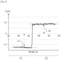
- the first level P1 brings together all the points recorded during the first passage of the wiper (outward) and the second P2 those recorded during the return of the wiper on the same track.
- )/2 and Fn 3N.
- the standard deviation of the points located on each level P1, P2 must be less than 0.1 to ensure good measurement accuracy. It is generally 0.05 for a tangential force equal to 0.5N. Consequently, if the standard deviation of the experimental data corresponding to the points of each level P1, P2 is greater than 0.1, these experimental data are not taken into account.
- This measurement mode consisting of a single round trip makes it possible to damage the surface tested as little as possible and to obtain reproducible measurements most often and depending on the type of friction pad.
- the appearance of the experimental data collected for a measurement of the friction coefficient of the electrochromic stack protected by the protective layer are for example represented on the Figure 3 .
- the coefficient of friction determined from the experimental data shown in this figure is equal to approximately 0.5.
- Scratch resistance is for example measured using a scratch resistance testing device such as those marketed by the Erichsen company.
- the assembly comprising the optical element 20 and the protective layer 3 has a coefficient of friction ⁇ which decreases more quickly than the coefficient of friction ⁇ i of the optical element 20 without a protective layer following organic contamination, this coefficient of friction being determined by a standardized tribometric measurement such as that described above.
- the assembly comprising the optical element 20 and the protective layer 3 has a coefficient of friction which reaches a value less than 0.5, preferably less than 0.4, preferably less than 0.3 in a time including between 1 and 100 hours.
- the progressive reduction in the coefficient of friction of the external face 11 of the optical system 10 according to the invention is due to the capacity of this layer protection 3 to adsorb organic compounds such as hydrocarbon compounds on its surface.
- organic compounds help to reduce the coefficient of friction and increase scratch resistance because the organic compounds adsorbed on the surface of the protective layer act as an additional sacrificial layer during friction.
- the optical system 10 according to the invention may further comprise an additional protective layer 4 comprising an organic compound which covers said protective layer 3. This is the case for example in the optical system 10 of the figure 1 .
- This organic compound comprises, for example, carbon, in particular amorphous carbon or diamond-type carbon.
- This additional protective layer 4 has for example a thickness of between 1 and 10 nanometers, preferably between 2 and 5 nanometers, preferably between 2 and 4 nanometers, preferably between 2 and 3 nanometers.
- the additional protective layer 4 is preferably removable by heat treatment at a temperature between 300 and 500°C.
- the additional protection layer 4 protects the electrochromic stack 2 and the protection layer 3 for all the processing steps and all the manipulations of the optical system 10 occurring before the quenching of this optical system 10.
- the optical system 10 is heated to temperatures typically above 500°Celsius, for example around 650°Celsius, and then cooled rapidly. This makes it possible to improve the mechanical properties of the substrate, particularly when it is made of glass.
- This quenching step eliminates the additional protective layer 4.
- the protective layer 3 is on the contrary retained. This protective layer 3 remains on the surface of the electrochromic stack 2 after quenching and continues to protect it during the processing steps and manipulations of the optical system 10 occurring after quenching.
- the additional protective layer 4 being eliminated by the tempering of the optical system 10, it can have any optical characteristic, in particular being opaque, that is to say having a very low transmission coefficient, for example less than 50%.
- this additional protection layer 4 is eliminated by a processing step of the already existing optical system. It is therefore not necessary to modify the processing of the optical system.
- the optical system 10 may further comprise, between said substrate 1 and the first transparent conductive layer of the electrochronic stack 2, a sub-layer preferably comprising an alternation of layers of high index material, for example a layer based on nobium oxide or titanium oxide and layers of a low index material, for example a layer based on silicon oxide.
- Said sublayer preferably has a thickness less than or equal to 100 nanometers, preferably less than or equal to 90 nanometers, preferably less than or equal to 80 nanometers, preferably less than or equal to 70 nanometers, preferably less than or equal to 60 nanometers, preferably less than or equal to 50 nanometers, preferably less than or equal to 40 nanometers, preferably less than or equal to 30 nanometers, preferably less than or equal to 30 nanometers, preferably less than or equal to 20 nanometers, preferably less or equal to 10 nanometers.
- This sublayer comprises for example a layer of 10 nanometers of niobium oxide or titanium oxide and a layer of 20 nanometers of silica oxide.
- Such an underlayer makes it possible in particular to prevent the diffusion of alkalis from the substrate towards the electrochromic stack.
- the optical system 10 can also comprise an over-layer arranged, for example deposited, on the second transparent conductive layer of the electrochronic stack 2 preferably comprising a layer of a low index material, for example a layer of carbon oxide. silicon, or an alternation of layers of high index and low index material, for example an alternation of layers based on silicon nitride and silicon oxide.
- Said over-layer preferably has a thickness less than or equal to 100 nanometers, preferably less than or equal to 90 nanometers, preferably less than or equal to 80 nanometers, preferably less than or equal to 70 nanometers, preferably less than or equal to 60 nanometers, preferably less than or equal to 50 nanometers, preferably less than or equal to 40 nanometers, preferably less than or equal to 30 nanometers, preferably less than or equal to 20 nanometers, preferably less than or equal to 10 nanometers.
- This over-layer includes, for example, a layer of 70 nanometers of silicon dioxide. Such an over-layer makes it possible in particular to control the color in transmission and the light transmission of the electrochromic stack.
- the term low index material means a material with an index less than 1.8.
- the optical system 10 described above can in particular be used in building glazing, in particular exterior glazing of internal partition or glass door, as glazing equipping internal partitions or windows of means of transport of the train type , plane, car, boat, as display screen glazing of the computer or television screen type, for camera lenses or solar panel protections.
- the invention thus also relates to insulating glazing comprising an optical system 10 as described above, a spacer and another substrate with a glass function assembled together.
- the inert gas may in particular be argon.
- the method according to the invention also comprises a step S3 of arranging the additional protective layer 4 on the protective layer 3.
- this method comprises at least one of the following steps: a cutting step S4 of the substrate 1 with a glass function, and/or a step of quenching S5 of the substrate 1 with a glass function after the step of forming the stack electrochromic 2.
- the cutting step takes place after the arrangement of the protective layer 3 and possibly the additional protective layer 4, before the quenching step SS of the optical system.
- the invention finally relates to a method of protecting the optical element 20 comprising the substrate 1 with a glass function and the electrochromic stack 2 formed on this substrate 1, comprising a step of arranging the protective layer 3 on said electrochromic stack 2.
- This may in particular be a step of deposition of the protective layer 3, in particular a step of magnetron deposition.
- the method according to the invention it is possible to protect the optical element 20 comprising the electrochromic stack 2 in a simple and effective manner, in particular for all the handling steps necessary during the manufacture and installation of glazing comprising such an optical element 10 taking place after the arrangement of the protective layer.
- This additional protection layer 4 provides temporary additional protection, limited to certain stages of use of the optical element.
- the electrochromic stack of the optical system according to the invention is protected in a simple and effective manner against friction and therefore against scratches which may be caused by this friction.
- the protective layer also limits the risk of damage to the electrochromic stack due to chemical corrosion.
Landscapes
- Physics & Mathematics (AREA)
- Chemical & Material Sciences (AREA)
- Nonlinear Science (AREA)
- Engineering & Computer Science (AREA)
- General Physics & Mathematics (AREA)
- Optics & Photonics (AREA)
- Chemical Kinetics & Catalysis (AREA)
- Materials Engineering (AREA)
- Organic Chemistry (AREA)
- Life Sciences & Earth Sciences (AREA)
- General Chemical & Material Sciences (AREA)
- Geochemistry & Mineralogy (AREA)
- Thermal Sciences (AREA)
- Health & Medical Sciences (AREA)
- Manufacturing & Machinery (AREA)
- Ophthalmology & Optometry (AREA)
- Mechanical Engineering (AREA)
- Electrochemistry (AREA)
- Inorganic Chemistry (AREA)
- Mathematical Physics (AREA)
- Crystallography & Structural Chemistry (AREA)
- Electrochromic Elements, Electrophoresis, Or Variable Reflection Or Absorption Elements (AREA)
- Surface Treatment Of Glass (AREA)
- Laminated Bodies (AREA)
Claims (20)
- Optisches System (10), umfassend:- ein optisches Element (20), umfassend ein Substrat (1) mit Glasfunktion und einen elektrochromen Stapel (2), der auf diesem Substrat (1) ausgebildet ist, wobei dieser elektrochrome Stapel (2) beinhaltet: eine erste transparente leitende Schicht, eine Arbeitselektrode, die über der ersten transparenten leitenden Schicht angeordnet ist, eine Gegenelektrode, die über der Arbeitselektrode angeordnet ist, eine zweite transparente leitende Schicht, die über der Gegenelektrode angeordnet ist, Lithiumionen, die in den elektrochromen Stapel eingeführt werden, und vorzugsweise eine Schicht aus einem separaten lonenleiter, die zwischen der Elektrode und der Gegenelektrode eingefügt ist,- eine Schutzschicht (3), die auf dem elektrochromen Stapel (2) angeordnet ist, die Schutzschicht (3) umfassend eine anorganische Schmiermittelverbindung, dadurch gekennzeichnet, dass die Schutzschicht (3) eine Dicke, die zwischen 1 und 30 Nanometer, vorzugsweise zwischen 2 und 15 Nanometer, vorzugsweise zwischen 2 und 10 Nanometer, vorzugsweise zwischen 2 und 5 Nanometer, liegt, aufweist.
- Optisches System (10) nach Anspruch 1, wobei die anorganische Schmiermittelverbindung mindestens eine der folgenden Verbindungen umfasst: Titanoxid TiOx, Zinn-Zink-Oxid SnZnOx, Titan-Strontium-Oxid TiSrOx, Titan-Zirkonium-Oxynitrid TiZrOxNy, Zirkoniumoxid ZrOx.
- Optisches System (10) nach einem der Ansprüche 1 und 2, wobei der Unterschied in der Lichtdurchlässigkeit zwischen dem optischen Element (20) und der Baugruppe, umfassend das optische Element (20) und die Schutzschicht (3), kleiner als oder gleich 5 % der Durchlässigkeit des optischen Elements (20), vorzugsweise kleiner als oder gleich 4 % der Durchlässigkeit des optischen Elements, vorzugsweise kleiner als oder gleich 3 % der Durchlässigkeit des optischen Elements, vorzugsweise kleiner als oder gleich 2 % der Durchlässigkeit des optischen Elements, vorzugsweise kleiner als oder gleich 1 % der Durchlässigkeit des optischen Elements ist.
- Optisches System (10) nach einem der Ansprüche 1 bis 3, wobei die Schutzschicht (3) auf dem elektrochromen Stapel (2) so angeordnet ist, dass sie einem Härtungsschritt standhält, bei dem das optische System (10) auf Temperaturen von mehr als 500 °Celsius, zum Beispiel etwa 650 °Celsius, erhitzt und dann schnell abgekühlt wird.
- Optisches System (10) nach einem der Ansprüche 1 bis 4, wobei die Baugruppe, umfassend das optische Element (10) und die Schutzschicht (3), einen Reibungskoeffizienten (µ) aufweist, der in Bezug auf den Reibungskoeffizienten (µi) des optischen Elements (20) ohne Schutzschicht (3) reduziert ist, wobei jeder Reibungskoeffizient durch eine standardisierte tribometrische Messung bestimmt wird.
- Optisches System (10) nach einem der Ansprüche 1 bis 5, wobei die Baugruppe, umfassend das optische Element (20) und die Schutzschicht (3), einen Reibungskoeffizienten (µ) aufweist, der den Reibungskoeffizienten (µi) des optischen Elements (20) ohne Schutzschicht (3) infolge organischer Verunreinigungen verringert, wobei jeder Reibungskoeffizient durch eine standardisierte tribometrische Messung bestimmt wird.
- Optisches System (10) nach einem der Ansprüche 1 bis 6, wobei die Baugruppe, umfassend das optische Element (20) und die Schutzschicht (3), einen Reibungskoeffizienten (µ) aufweist, der einen Wert von kleiner als 0,5, vorzugsweise kleiner als 0,4, vorzugsweise kleiner als 0,3, in einer Zeit, die zwischen 1 und 100 Stunden liegt, erreicht.
- Optisches System (10) nach einem der Ansprüche 1 bis 7, wobei das Substrat (1) gehärtet ist.
- Optisches System (10) nach einem der Ansprüche 1 bis 8, wobei eine zusätzliche Schutzschicht (4) vorgesehen ist, umfassend eine organische Verbindung, die die Schutzschicht (3) bedeckt.
- Optisches System (10) nach Anspruch 9, wobei die organische Verbindung Kohlenstoff umfasst.
- Optisches System (10) nach einem der Ansprüche 9 und 10, wobei die zusätzliche Schutzschicht (4) eine Dicke, die zwischen 1 und 10 Nanometer, vorzugsweise zwischen 2 und 5 Nanometer, liegt, aufweist.
- Optisches System (10) nach einem der Ansprüche 9 bis 11, wobei die zusätzliche Schutzschicht (4) durch eine Wärmebehandlung bei einer Temperatur, die zwischen 300 und 500 °C liegt, entfernbar ist.
- Optisches System (10) nach einem der Ansprüche 1 bis 12, wobei:- die Arbeitselektrode aus einem elektrochromen Material, vorzugsweise basierend auf Wolframoxid WOx oder Wolfram-Lithium-Oxid LiWOx, gefertigt ist, und die Gegenelektrode vorzugsweise aus einem Oxid einer Wolfram-NickelLegierung gefertigt ist,- die lonenleiterschicht vorzugsweise eine Schicht aus Siliziumoxid SiOx umfasst,- die erste und eine zweite transparente leitende Schicht vorzugsweise basierend auf Indium-Zinn-Oxid (ITO) gefertigt sind.
- Optisches System (10) nach Anspruch 13, ferner umfassend, zwischen dem Substrat (1) und der ersten transparenten leitenden Schicht, eine Unterschicht, umfassend vorzugsweise eine Abfolge aus mindestens einer Schicht basierend auf Nobiumoxid und mindestens einer Schicht basierend auf Siliziumoxid.
- Optisches System (10) nach einem der Ansprüche 13 und 14, ferner umfassend eine Überschicht, die auf der zweiten transparenten leitenden Schicht angeordnet ist, umfassend vorzugsweise eine Schicht basierend auf Siliziumoxid.
- Isolierverglasung, umfassend ein optisches System (10) nach einem der Ansprüche 1 bis 15, einen Abstandhalter und ein weiteres Substrat mit Glasfunktion, die miteinander zusammengefügt sind.
- Verfahren zum Herstellen einer Isolierverglasung, umfassend ein optisches System (10) nach einem der Ansprüche 1 bis 15, das Verfahren umfassend die folgenden Schritte:- Ausbilden des elektrochromen Stapels (2) auf dem Substrat (1) mit Glasfunktion,- Anordnen der Schutzschicht (3) auf dem elektrochromen Stapel (2),- Manipulieren und/oder Bearbeiten und/oder Behandeln und/oder Transportieren und/oder Waschen und/oder Lagern des optischen Systems (10),- vorzugsweise Zusammenbauen durch Laminieren der Fläche des Substrats (1) mit Glasfunktion, die derjenigen gegenüberliegt, die auf der Seite des elektrochromen Stapels (2) liegt, mit einem Gegensubstrat,- Zusammenbauen des optischen Systems (10), das optional laminiert ist, mit einem Abstandhalter und einem zweiten Substrat mit Glasfunktion, um die Isolierverglasung auszubilden.
- Verfahren zum Herstellen einer Isolierverglasung nach Anspruch 17, umfassend mindestens einen der folgenden Schritte:- einen Schritt zum Schneiden des Substrats (1) mit Glasfunktion,- einen Schritt des Härtens des Substrats (1) mit Glasfunktion nach dem Schritt des Ausbildens des elektrochromen Stapels (2).
- Verfahren zum Schützen eines optischen Elements (10), umfassend ein Substrat (1) mit Glasfunktion und einen elektrochromen Stapel (2), der auf diesem Substrat (1) ausgebildet wird, wobei dieser elektrochrome Stapel beinhaltet: eine erste transparente leitende Schicht, eine Arbeitselektrode, die über der ersten transparenten leitenden Schicht angeordnet ist, eine Gegenelektrode, die über der Arbeitselektrode angeordnet ist, eine zweite transparente leitende Schicht, die über der Gegenelektrode angeordnet ist, Lithiumionen, die innerhalb des elektrochromen Stapels eingeführt werden, und vorzugsweise eine Schicht eines separaten lonenleiters, die zwischen der Elektrode und der Gegenelektrode eingefügt ist, das Verfahren umfassend einen Schritt des Anordnens einer Schutzschicht (3) auf dem elektrochromen Stapel (2), die Schutzschicht (3) umfassend eine anorganische Schmiermittelverbindung, dadurch gekennzeichnet, dass die Schutzschicht (3) eine Dicke, die zwischen 1 und 30 Nanometer, vorzugsweise zwischen 2 und 15 Nanometer, vorzugsweise zwischen 2 und 10 Nanometer, vorzugsweise zwischen 2 und 5 Nanometer, liegt, aufweist.
- Verfahren nach Anspruch 19, wobei ein zusätzlicher Schritt des Anordnens einer zusätzlichen Schutzschicht (4), die die Schutzschicht (3) bedeckt, vorgesehen ist, die zusätzliche Schutzschicht (4) umfassend eine organische Verbindung und einen nachfolgenden Schritt des Entfernens der zusätzlichen Schutzschicht (4) durch eine Wärmebehandlung bei einer Temperatur, die zwischen 300 und 500 °C liegt.
Applications Claiming Priority (2)
| Application Number | Priority Date | Filing Date | Title |
|---|---|---|---|
| FR2000008A FR3106006B1 (fr) | 2020-01-02 | 2020-01-02 | Système optique, vitrage isolant comportant un tel système optique, procédé de fabrication de ce vitrage isolant et procédé de protection d’un système optique |
| PCT/FR2020/052635 WO2021136914A1 (fr) | 2020-01-02 | 2020-12-28 | Système optique, vitrage isolant comportant un tel système optique, procédé de fabrication de ce vitrage isolant et procédé de protection d'un système optique |
Publications (2)
| Publication Number | Publication Date |
|---|---|
| EP4085299A1 EP4085299A1 (de) | 2022-11-09 |
| EP4085299B1 true EP4085299B1 (de) | 2023-11-08 |
Family
ID=69903610
Family Applications (1)
| Application Number | Title | Priority Date | Filing Date |
|---|---|---|---|
| EP20851235.0A Active EP4085299B1 (de) | 2020-01-02 | 2020-12-28 | Optisches system, isolierverglasung, die ein solches optisches system umfasst, verfahren zum herstellen dieser isolierverglasung und verfahren zum schützen eines optischen systems |
Country Status (7)
| Country | Link |
|---|---|
| US (1) | US20230033668A1 (de) |
| EP (1) | EP4085299B1 (de) |
| JP (1) | JP2023509393A (de) |
| CN (1) | CN114787706A (de) |
| FR (1) | FR3106006B1 (de) |
| TW (1) | TW202136169A (de) |
| WO (1) | WO2021136914A1 (de) |
Families Citing this family (1)
| Publication number | Priority date | Publication date | Assignee | Title |
|---|---|---|---|---|
| CN116880107A (zh) * | 2023-05-06 | 2023-10-13 | 浙江景昇薄膜科技有限公司 | 一种电致变色材料及其制备方法 |
Family Cites Families (20)
| Publication number | Priority date | Publication date | Assignee | Title |
|---|---|---|---|---|
| FR2601150B1 (fr) | 1986-07-04 | 1991-05-31 | Saint Gobain Vitrage | Vitrage a transmission variable du type electrochrome |
| FR2642890B1 (fr) | 1989-02-09 | 1991-04-12 | Saint Gobain Vitrage | Materiau colloide conducteur de cations alcalins et applications a titre d'electrolytes |
| FR2677800B1 (fr) | 1991-06-14 | 1993-08-20 | Saint Gobain Vitrage Int | Materiau solide conducteur ionique, a partir d'un polymere et d'un sel de cation alcalin, application comme electrolyte. |
| EP0532408A1 (de) | 1991-09-13 | 1993-03-17 | Saint-Gobain Vitrage International | Protonenleitendes Polymer und seine Verwendung als Elektrolyt in elektrochemischen Verbindungen |
| RU2117971C1 (ru) * | 1992-04-10 | 1998-08-20 | Сан Эктив Гласс Электрокромикс, Инк. | Электрохромное устройство (варианты) и способ его изготовления (варианты) |
| FR2716457B1 (fr) | 1994-02-23 | 1996-05-24 | Saint Gobain Vitrage Int | Matériau électrolyte conducteur protonique. |
| FR2746934B1 (fr) | 1996-03-27 | 1998-05-07 | Saint Gobain Vitrage | Dispositif electrochimique |
| FR2753545B1 (fr) | 1996-09-18 | 1998-10-16 | Saint Gobain Vitrage | Dispositif electrochimique |
| KR19980070792A (ko) * | 1997-01-23 | 1998-10-26 | 오오자와 히데지로오 | 일렉트로크로믹 장치 |
| FR2791147B1 (fr) | 1999-03-19 | 2002-08-30 | Saint Gobain Vitrage | Dispositif electrochimique du type dispositif electrocommandable a proprietes optiques et/ou energetiques variables |
| US6770321B2 (en) * | 2002-01-25 | 2004-08-03 | Afg Industries, Inc. | Method of making transparent articles utilizing protective layers for optical coatings |
| WO2012177790A2 (en) * | 2011-06-21 | 2012-12-27 | Soladigm, Inc. | Temperable electrochromic devices |
| WO2016203305A1 (ja) * | 2015-06-15 | 2016-12-22 | 王子ホールディングス株式会社 | 加飾用積層体 |
| AT15220U1 (de) * | 2016-03-07 | 2017-03-15 | Ceratizit Austria Gmbh | Verfahren zur Herstellung einer Hartstoffschicht auf einem Substrat, Hartstoffschicht, Zerspanwerkzeug sowie Beschichtungsquelle |
| US20190177219A1 (en) * | 2016-06-03 | 2019-06-13 | Raymond Miller Karam | Method and apparatus for vacuum insulated glazings |
| JP7175607B2 (ja) * | 2017-12-27 | 2022-11-21 | 株式会社パイロットコーポレーション | 筆記シート |
| CN108227328B (zh) * | 2018-01-30 | 2024-12-13 | 林嘉佑 | 一种改良型电控全固态智能调光装置 |
| CN207875047U (zh) * | 2018-02-08 | 2018-09-18 | 杭州富阳诚科通信材料有限公司 | 一种防静电色母粒 |
| CN110223604A (zh) * | 2019-05-27 | 2019-09-10 | 武汉华星光电半导体显示技术有限公司 | 一种显示面板用的柔性盖板及其制备方法、显示装置 |
| JP6609085B1 (ja) * | 2019-07-05 | 2019-11-20 | 中部電力株式会社 | 漏油検出材 |
-
2020
- 2020-01-02 FR FR2000008A patent/FR3106006B1/fr active Active
- 2020-12-28 US US17/788,122 patent/US20230033668A1/en active Pending
- 2020-12-28 CN CN202080089270.8A patent/CN114787706A/zh active Pending
- 2020-12-28 WO PCT/FR2020/052635 patent/WO2021136914A1/fr not_active Ceased
- 2020-12-28 EP EP20851235.0A patent/EP4085299B1/de active Active
- 2020-12-28 JP JP2022538467A patent/JP2023509393A/ja active Pending
- 2020-12-30 TW TW109146883A patent/TW202136169A/zh unknown
Also Published As
| Publication number | Publication date |
|---|---|
| FR3106006A1 (fr) | 2021-07-09 |
| CN114787706A (zh) | 2022-07-22 |
| JP2023509393A (ja) | 2023-03-08 |
| TW202136169A (zh) | 2021-10-01 |
| US20230033668A1 (en) | 2023-02-02 |
| WO2021136914A1 (fr) | 2021-07-08 |
| FR3106006B1 (fr) | 2023-10-27 |
| EP4085299A1 (de) | 2022-11-09 |
Similar Documents
| Publication | Publication Date | Title |
|---|---|---|
| EP1012662B1 (de) | Verfahren zur behandlung einer elektrochemischen vorrichtung | |
| EP2307926B1 (de) | Elektrochromes bauelement mit gesteuerter infrarotreflexion | |
| EP1952194B1 (de) | Elektrochromes system auf einem kunststoffsubstrat | |
| EP0486387A1 (de) | Elektrochromes Fenster | |
| FR2753545A1 (fr) | Dispositif electrochimique | |
| FR2962818A1 (fr) | Dispositif electrochimique a proprietes de transmission optique et/ou energetique electrocommandables. | |
| WO2003048843A2 (fr) | Electrode de dispositifs electrochimiques/electrocommandables | |
| EP2084574A2 (de) | Transparente schicht mit hoher elektrischer leitfähigkeit mit metallgitter mit optimiertem elektrochemischem widerstand | |
| WO2012076799A1 (fr) | Dipositif electrochimique a proprietes de transmission optique et/ou energetique electrococommandables | |
| WO2006092532A2 (fr) | Dispositif electrocommandable a proprietes optiques et/ou energetique variables et son procede d'alimentation | |
| EP4085299B1 (de) | Optisches system, isolierverglasung, die ein solches optisches system umfasst, verfahren zum herstellen dieser isolierverglasung und verfahren zum schützen eines optischen systems | |
| CA2003386A1 (fr) | Contre-electrode pour systemes electrochromes | |
| FR2669122A1 (fr) | Vitrage electrochrome. | |
| WO2021123267A1 (fr) | Trempe thermique d'une electrode travail | |
| EP3938332A1 (de) | Verfahren zum schützen eines mit einem elektrochromen stapel beschichteten glassubstrats und verfahren zur herstellung einer isolierverglasung | |
| WO2012076800A1 (fr) | Dispositif electrochimique a proprietes de transmission optique et/ou energetique electrocommandables | |
| EP4081858B1 (de) | Optisches system mit einer elektrochemischen funktionsvorrichtung mit elektrisch steuerbaren optischen und/oder energetischen eigenschaften und einer beschichtung zum steuern der farbe in reflexion und zugehörige verfahren | |
| WO2010004158A1 (fr) | Electrode isolante pour dispositif électrochimique | |
| EP4602434A1 (de) | Elektrochrome verglasung | |
| EP0770900A1 (de) | Elektrochrome Verglasung | |
| EP4543818A1 (de) | Transparenter glasartikel für ein kühlfach und mehrfachverglasungseinheit mit dem artikel | |
| FR3137084A1 (fr) | Article verrier transparent pour compartiment froid et vitrage multiple incorporant ledit article. | |
| EP4602435A1 (de) | Elektrochrome verglasung | |
| FR2719914A1 (fr) | Vitrage électrochrome. |
Legal Events
| Date | Code | Title | Description |
|---|---|---|---|
| STAA | Information on the status of an ep patent application or granted ep patent |
Free format text: STATUS: UNKNOWN |
|
| STAA | Information on the status of an ep patent application or granted ep patent |
Free format text: STATUS: THE INTERNATIONAL PUBLICATION HAS BEEN MADE |
|
| PUAI | Public reference made under article 153(3) epc to a published international application that has entered the european phase |
Free format text: ORIGINAL CODE: 0009012 |
|
| STAA | Information on the status of an ep patent application or granted ep patent |
Free format text: STATUS: REQUEST FOR EXAMINATION WAS MADE |
|
| 17P | Request for examination filed |
Effective date: 20220802 |
|
| AK | Designated contracting states |
Kind code of ref document: A1 Designated state(s): AL AT BE BG CH CY CZ DE DK EE ES FI FR GB GR HR HU IE IS IT LI LT LU LV MC MK MT NL NO PL PT RO RS SE SI SK SM TR |
|
| DAV | Request for validation of the european patent (deleted) | ||
| DAX | Request for extension of the european patent (deleted) | ||
| GRAP | Despatch of communication of intention to grant a patent |
Free format text: ORIGINAL CODE: EPIDOSNIGR1 |
|
| STAA | Information on the status of an ep patent application or granted ep patent |
Free format text: STATUS: GRANT OF PATENT IS INTENDED |
|
| RIC1 | Information provided on ipc code assigned before grant |
Ipc: B32B 17/06 20060101ALI20230508BHEP Ipc: B32B 17/10 20060101ALI20230508BHEP Ipc: G02F 1/153 20060101AFI20230508BHEP |
|
| INTG | Intention to grant announced |
Effective date: 20230601 |
|
| GRAS | Grant fee paid |
Free format text: ORIGINAL CODE: EPIDOSNIGR3 |
|
| GRAA | (expected) grant |
Free format text: ORIGINAL CODE: 0009210 |
|
| STAA | Information on the status of an ep patent application or granted ep patent |
Free format text: STATUS: THE PATENT HAS BEEN GRANTED |
|
| AK | Designated contracting states |
Kind code of ref document: B1 Designated state(s): AL AT BE BG CH CY CZ DE DK EE ES FI FR GB GR HR HU IE IS IT LI LT LU LV MC MK MT NL NO PL PT RO RS SE SI SK SM TR |
|
| REG | Reference to a national code |
Ref country code: GB Ref legal event code: FG4D Free format text: NOT ENGLISH |
|
| REG | Reference to a national code |
Ref country code: CH Ref legal event code: EP |
|
| REG | Reference to a national code |
Ref country code: DE Ref legal event code: R096 Ref document number: 602020020865 Country of ref document: DE |
|
| REG | Reference to a national code |
Ref country code: IE Ref legal event code: FG4D Free format text: LANGUAGE OF EP DOCUMENT: FRENCH |
|
| REG | Reference to a national code |
Ref country code: NL Ref legal event code: FP |
|
| P01 | Opt-out of the competence of the unified patent court (upc) registered |
Effective date: 20231124 |
|
| PGFP | Annual fee paid to national office [announced via postgrant information from national office to epo] |
Ref country code: NL Payment date: 20231215 Year of fee payment: 4 |
|
| REG | Reference to a national code |
Ref country code: LT Ref legal event code: MG9D |
|
| PGFP | Annual fee paid to national office [announced via postgrant information from national office to epo] |
Ref country code: BE Payment date: 20231219 Year of fee payment: 4 |
|
| PG25 | Lapsed in a contracting state [announced via postgrant information from national office to epo] |
Ref country code: GR Free format text: LAPSE BECAUSE OF FAILURE TO SUBMIT A TRANSLATION OF THE DESCRIPTION OR TO PAY THE FEE WITHIN THE PRESCRIBED TIME-LIMIT Effective date: 20240209 |
|
| PG25 | Lapsed in a contracting state [announced via postgrant information from national office to epo] |
Ref country code: IS Free format text: LAPSE BECAUSE OF FAILURE TO SUBMIT A TRANSLATION OF THE DESCRIPTION OR TO PAY THE FEE WITHIN THE PRESCRIBED TIME-LIMIT Effective date: 20240308 |
|
| PG25 | Lapsed in a contracting state [announced via postgrant information from national office to epo] |
Ref country code: LT Free format text: LAPSE BECAUSE OF FAILURE TO SUBMIT A TRANSLATION OF THE DESCRIPTION OR TO PAY THE FEE WITHIN THE PRESCRIBED TIME-LIMIT Effective date: 20231108 |
|
| REG | Reference to a national code |
Ref country code: AT Ref legal event code: MK05 Ref document number: 1630152 Country of ref document: AT Kind code of ref document: T Effective date: 20231108 |
|
| PG25 | Lapsed in a contracting state [announced via postgrant information from national office to epo] |
Ref country code: AT Free format text: LAPSE BECAUSE OF FAILURE TO SUBMIT A TRANSLATION OF THE DESCRIPTION OR TO PAY THE FEE WITHIN THE PRESCRIBED TIME-LIMIT Effective date: 20231108 |
|
| PG25 | Lapsed in a contracting state [announced via postgrant information from national office to epo] |
Ref country code: ES Free format text: LAPSE BECAUSE OF FAILURE TO SUBMIT A TRANSLATION OF THE DESCRIPTION OR TO PAY THE FEE WITHIN THE PRESCRIBED TIME-LIMIT Effective date: 20231108 |
|
| PG25 | Lapsed in a contracting state [announced via postgrant information from national office to epo] |
Ref country code: LT Free format text: LAPSE BECAUSE OF FAILURE TO SUBMIT A TRANSLATION OF THE DESCRIPTION OR TO PAY THE FEE WITHIN THE PRESCRIBED TIME-LIMIT Effective date: 20231108 Ref country code: IS Free format text: LAPSE BECAUSE OF FAILURE TO SUBMIT A TRANSLATION OF THE DESCRIPTION OR TO PAY THE FEE WITHIN THE PRESCRIBED TIME-LIMIT Effective date: 20240308 Ref country code: GR Free format text: LAPSE BECAUSE OF FAILURE TO SUBMIT A TRANSLATION OF THE DESCRIPTION OR TO PAY THE FEE WITHIN THE PRESCRIBED TIME-LIMIT Effective date: 20240209 Ref country code: ES Free format text: LAPSE BECAUSE OF FAILURE TO SUBMIT A TRANSLATION OF THE DESCRIPTION OR TO PAY THE FEE WITHIN THE PRESCRIBED TIME-LIMIT Effective date: 20231108 Ref country code: BG Free format text: LAPSE BECAUSE OF FAILURE TO SUBMIT A TRANSLATION OF THE DESCRIPTION OR TO PAY THE FEE WITHIN THE PRESCRIBED TIME-LIMIT Effective date: 20240208 Ref country code: AT Free format text: LAPSE BECAUSE OF FAILURE TO SUBMIT A TRANSLATION OF THE DESCRIPTION OR TO PAY THE FEE WITHIN THE PRESCRIBED TIME-LIMIT Effective date: 20231108 Ref country code: PT Free format text: LAPSE BECAUSE OF FAILURE TO SUBMIT A TRANSLATION OF THE DESCRIPTION OR TO PAY THE FEE WITHIN THE PRESCRIBED TIME-LIMIT Effective date: 20240308 |
|
| PG25 | Lapsed in a contracting state [announced via postgrant information from national office to epo] |
Ref country code: SE Free format text: LAPSE BECAUSE OF FAILURE TO SUBMIT A TRANSLATION OF THE DESCRIPTION OR TO PAY THE FEE WITHIN THE PRESCRIBED TIME-LIMIT Effective date: 20231108 Ref country code: RS Free format text: LAPSE BECAUSE OF FAILURE TO SUBMIT A TRANSLATION OF THE DESCRIPTION OR TO PAY THE FEE WITHIN THE PRESCRIBED TIME-LIMIT Effective date: 20231108 Ref country code: PL Free format text: LAPSE BECAUSE OF FAILURE TO SUBMIT A TRANSLATION OF THE DESCRIPTION OR TO PAY THE FEE WITHIN THE PRESCRIBED TIME-LIMIT Effective date: 20231108 Ref country code: NO Free format text: LAPSE BECAUSE OF FAILURE TO SUBMIT A TRANSLATION OF THE DESCRIPTION OR TO PAY THE FEE WITHIN THE PRESCRIBED TIME-LIMIT Effective date: 20240208 Ref country code: LV Free format text: LAPSE BECAUSE OF FAILURE TO SUBMIT A TRANSLATION OF THE DESCRIPTION OR TO PAY THE FEE WITHIN THE PRESCRIBED TIME-LIMIT Effective date: 20231108 Ref country code: HR Free format text: LAPSE BECAUSE OF FAILURE TO SUBMIT A TRANSLATION OF THE DESCRIPTION OR TO PAY THE FEE WITHIN THE PRESCRIBED TIME-LIMIT Effective date: 20231108 |
|
| PG25 | Lapsed in a contracting state [announced via postgrant information from national office to epo] |
Ref country code: DK Free format text: LAPSE BECAUSE OF FAILURE TO SUBMIT A TRANSLATION OF THE DESCRIPTION OR TO PAY THE FEE WITHIN THE PRESCRIBED TIME-LIMIT Effective date: 20231108 |
|
| PG25 | Lapsed in a contracting state [announced via postgrant information from national office to epo] |
Ref country code: CZ Free format text: LAPSE BECAUSE OF FAILURE TO SUBMIT A TRANSLATION OF THE DESCRIPTION OR TO PAY THE FEE WITHIN THE PRESCRIBED TIME-LIMIT Effective date: 20231108 |
|
| PG25 | Lapsed in a contracting state [announced via postgrant information from national office to epo] |
Ref country code: SK Free format text: LAPSE BECAUSE OF FAILURE TO SUBMIT A TRANSLATION OF THE DESCRIPTION OR TO PAY THE FEE WITHIN THE PRESCRIBED TIME-LIMIT Effective date: 20231108 |
|
| PG25 | Lapsed in a contracting state [announced via postgrant information from national office to epo] |
Ref country code: SM Free format text: LAPSE BECAUSE OF FAILURE TO SUBMIT A TRANSLATION OF THE DESCRIPTION OR TO PAY THE FEE WITHIN THE PRESCRIBED TIME-LIMIT Effective date: 20231108 Ref country code: SK Free format text: LAPSE BECAUSE OF FAILURE TO SUBMIT A TRANSLATION OF THE DESCRIPTION OR TO PAY THE FEE WITHIN THE PRESCRIBED TIME-LIMIT Effective date: 20231108 Ref country code: RO Free format text: LAPSE BECAUSE OF FAILURE TO SUBMIT A TRANSLATION OF THE DESCRIPTION OR TO PAY THE FEE WITHIN THE PRESCRIBED TIME-LIMIT Effective date: 20231108 Ref country code: IT Free format text: LAPSE BECAUSE OF FAILURE TO SUBMIT A TRANSLATION OF THE DESCRIPTION OR TO PAY THE FEE WITHIN THE PRESCRIBED TIME-LIMIT Effective date: 20231108 Ref country code: EE Free format text: LAPSE BECAUSE OF FAILURE TO SUBMIT A TRANSLATION OF THE DESCRIPTION OR TO PAY THE FEE WITHIN THE PRESCRIBED TIME-LIMIT Effective date: 20231108 Ref country code: DK Free format text: LAPSE BECAUSE OF FAILURE TO SUBMIT A TRANSLATION OF THE DESCRIPTION OR TO PAY THE FEE WITHIN THE PRESCRIBED TIME-LIMIT Effective date: 20231108 Ref country code: CZ Free format text: LAPSE BECAUSE OF FAILURE TO SUBMIT A TRANSLATION OF THE DESCRIPTION OR TO PAY THE FEE WITHIN THE PRESCRIBED TIME-LIMIT Effective date: 20231108 |
|
| REG | Reference to a national code |
Ref country code: DE Ref legal event code: R097 Ref document number: 602020020865 Country of ref document: DE |
|
| PG25 | Lapsed in a contracting state [announced via postgrant information from national office to epo] |
Ref country code: LU Free format text: LAPSE BECAUSE OF NON-PAYMENT OF DUE FEES Effective date: 20231228 |
|
| PG25 | Lapsed in a contracting state [announced via postgrant information from national office to epo] |
Ref country code: MC Free format text: LAPSE BECAUSE OF FAILURE TO SUBMIT A TRANSLATION OF THE DESCRIPTION OR TO PAY THE FEE WITHIN THE PRESCRIBED TIME-LIMIT Effective date: 20231108 |
|
| PG25 | Lapsed in a contracting state [announced via postgrant information from national office to epo] |
Ref country code: MC Free format text: LAPSE BECAUSE OF FAILURE TO SUBMIT A TRANSLATION OF THE DESCRIPTION OR TO PAY THE FEE WITHIN THE PRESCRIBED TIME-LIMIT Effective date: 20231108 Ref country code: LU Free format text: LAPSE BECAUSE OF NON-PAYMENT OF DUE FEES Effective date: 20231228 |
|
| PLBE | No opposition filed within time limit |
Free format text: ORIGINAL CODE: 0009261 |
|
| STAA | Information on the status of an ep patent application or granted ep patent |
Free format text: STATUS: NO OPPOSITION FILED WITHIN TIME LIMIT |
|
| REG | Reference to a national code |
Ref country code: IE Ref legal event code: MM4A |
|
| PG25 | Lapsed in a contracting state [announced via postgrant information from national office to epo] |
Ref country code: IE Free format text: LAPSE BECAUSE OF NON-PAYMENT OF DUE FEES Effective date: 20231228 |
|
| 26N | No opposition filed |
Effective date: 20240809 |
|
| PG25 | Lapsed in a contracting state [announced via postgrant information from national office to epo] |
Ref country code: SI Free format text: LAPSE BECAUSE OF FAILURE TO SUBMIT A TRANSLATION OF THE DESCRIPTION OR TO PAY THE FEE WITHIN THE PRESCRIBED TIME-LIMIT Effective date: 20231108 |
|
| PG25 | Lapsed in a contracting state [announced via postgrant information from national office to epo] |
Ref country code: SI Free format text: LAPSE BECAUSE OF FAILURE TO SUBMIT A TRANSLATION OF THE DESCRIPTION OR TO PAY THE FEE WITHIN THE PRESCRIBED TIME-LIMIT Effective date: 20231108 Ref country code: IE Free format text: LAPSE BECAUSE OF NON-PAYMENT OF DUE FEES Effective date: 20231228 |
|
| PGFP | Annual fee paid to national office [announced via postgrant information from national office to epo] |
Ref country code: CH Payment date: 20250101 Year of fee payment: 5 |
|
| PG25 | Lapsed in a contracting state [announced via postgrant information from national office to epo] |
Ref country code: FI Free format text: LAPSE BECAUSE OF FAILURE TO SUBMIT A TRANSLATION OF THE DESCRIPTION OR TO PAY THE FEE WITHIN THE PRESCRIBED TIME-LIMIT Effective date: 20231108 |
|
| PG25 | Lapsed in a contracting state [announced via postgrant information from national office to epo] |
Ref country code: CY Free format text: LAPSE BECAUSE OF FAILURE TO SUBMIT A TRANSLATION OF THE DESCRIPTION OR TO PAY THE FEE WITHIN THE PRESCRIBED TIME-LIMIT; INVALID AB INITIO Effective date: 20201228 |
|
| REG | Reference to a national code |
Ref country code: NL Ref legal event code: MM Effective date: 20250101 |
|
| PG25 | Lapsed in a contracting state [announced via postgrant information from national office to epo] |
Ref country code: HU Free format text: LAPSE BECAUSE OF FAILURE TO SUBMIT A TRANSLATION OF THE DESCRIPTION OR TO PAY THE FEE WITHIN THE PRESCRIBED TIME-LIMIT; INVALID AB INITIO Effective date: 20201228 |
|
| GBPC | Gb: european patent ceased through non-payment of renewal fee |
Effective date: 20241228 |
|
| PG25 | Lapsed in a contracting state [announced via postgrant information from national office to epo] |
Ref country code: NL Free format text: LAPSE BECAUSE OF NON-PAYMENT OF DUE FEES Effective date: 20250101 |
|
| REG | Reference to a national code |
Ref country code: BE Ref legal event code: MM Effective date: 20241231 |
|
| PG25 | Lapsed in a contracting state [announced via postgrant information from national office to epo] |
Ref country code: GB Free format text: LAPSE BECAUSE OF NON-PAYMENT OF DUE FEES Effective date: 20241228 Ref country code: BE Free format text: LAPSE BECAUSE OF NON-PAYMENT OF DUE FEES Effective date: 20241231 |
|
| PG25 | Lapsed in a contracting state [announced via postgrant information from national office to epo] |
Ref country code: TR Free format text: LAPSE BECAUSE OF FAILURE TO SUBMIT A TRANSLATION OF THE DESCRIPTION OR TO PAY THE FEE WITHIN THE PRESCRIBED TIME-LIMIT Effective date: 20231108 |
|
| REG | Reference to a national code |
Ref country code: CH Ref legal event code: U11 Free format text: ST27 STATUS EVENT CODE: U-0-0-U10-U11 (AS PROVIDED BY THE NATIONAL OFFICE) Effective date: 20260101 |
|
| PGFP | Annual fee paid to national office [announced via postgrant information from national office to epo] |
Ref country code: DE Payment date: 20251104 Year of fee payment: 6 |
|
| PGFP | Annual fee paid to national office [announced via postgrant information from national office to epo] |
Ref country code: FR Payment date: 20251110 Year of fee payment: 6 |