EP4080590A1 - Light emitting device - Google Patents
Light emitting device Download PDFInfo
- Publication number
- EP4080590A1 EP4080590A1 EP22168969.8A EP22168969A EP4080590A1 EP 4080590 A1 EP4080590 A1 EP 4080590A1 EP 22168969 A EP22168969 A EP 22168969A EP 4080590 A1 EP4080590 A1 EP 4080590A1
- Authority
- EP
- European Patent Office
- Prior art keywords
- light emitting
- base
- upper face
- emitting element
- emitting device
- Prior art date
- Legal status (The legal status is an assumption and is not a legal conclusion. Google has not performed a legal analysis and makes no representation as to the accuracy of the status listed.)
- Granted
Links
Images


Classifications
-
- H—ELECTRICITY
- H10—SEMICONDUCTOR DEVICES; ELECTRIC SOLID-STATE DEVICES NOT OTHERWISE PROVIDED FOR
- H10H—INORGANIC LIGHT-EMITTING SEMICONDUCTOR DEVICES HAVING POTENTIAL BARRIERS
- H10H20/00—Individual inorganic light-emitting semiconductor devices having potential barriers, e.g. light-emitting diodes [LED]
- H10H20/80—Constructional details
- H10H20/85—Packages
- H10H20/857—Interconnections, e.g. lead-frames, bond wires or solder balls
-
- H—ELECTRICITY
- H10—SEMICONDUCTOR DEVICES; ELECTRIC SOLID-STATE DEVICES NOT OTHERWISE PROVIDED FOR
- H10H—INORGANIC LIGHT-EMITTING SEMICONDUCTOR DEVICES HAVING POTENTIAL BARRIERS
- H10H20/00—Individual inorganic light-emitting semiconductor devices having potential barriers, e.g. light-emitting diodes [LED]
- H10H20/80—Constructional details
- H10H20/84—Coatings, e.g. passivation layers or antireflective coatings
-
- H—ELECTRICITY
- H10—SEMICONDUCTOR DEVICES; ELECTRIC SOLID-STATE DEVICES NOT OTHERWISE PROVIDED FOR
- H10H—INORGANIC LIGHT-EMITTING SEMICONDUCTOR DEVICES HAVING POTENTIAL BARRIERS
- H10H20/00—Individual inorganic light-emitting semiconductor devices having potential barriers, e.g. light-emitting diodes [LED]
- H10H20/80—Constructional details
- H10H20/85—Packages
- H10H20/8506—Containers
-
- H—ELECTRICITY
- H10—SEMICONDUCTOR DEVICES; ELECTRIC SOLID-STATE DEVICES NOT OTHERWISE PROVIDED FOR
- H10H—INORGANIC LIGHT-EMITTING SEMICONDUCTOR DEVICES HAVING POTENTIAL BARRIERS
- H10H20/00—Individual inorganic light-emitting semiconductor devices having potential barriers, e.g. light-emitting diodes [LED]
- H10H20/80—Constructional details
- H10H20/85—Packages
- H10H20/852—Encapsulations
-
- H—ELECTRICITY
- H10—SEMICONDUCTOR DEVICES; ELECTRIC SOLID-STATE DEVICES NOT OTHERWISE PROVIDED FOR
- H10H—INORGANIC LIGHT-EMITTING SEMICONDUCTOR DEVICES HAVING POTENTIAL BARRIERS
- H10H20/00—Individual inorganic light-emitting semiconductor devices having potential barriers, e.g. light-emitting diodes [LED]
- H10H20/80—Constructional details
- H10H20/85—Packages
- H10H20/852—Encapsulations
- H10H20/854—Encapsulations characterised by their material, e.g. epoxy or silicone resins
-
- H—ELECTRICITY
- H10—SEMICONDUCTOR DEVICES; ELECTRIC SOLID-STATE DEVICES NOT OTHERWISE PROVIDED FOR
- H10H—INORGANIC LIGHT-EMITTING SEMICONDUCTOR DEVICES HAVING POTENTIAL BARRIERS
- H10H20/00—Individual inorganic light-emitting semiconductor devices having potential barriers, e.g. light-emitting diodes [LED]
- H10H20/01—Manufacture or treatment
- H10H20/034—Manufacture or treatment of coatings
Definitions
- the present disclosure relates to a light emitting device.
- Japanese Patent Publication No. 2018-6456 describes a light emitting device that includes a package, a light emitting element disposed in the package, a bonding member disposed on the upper face of the package, and a light transmissive member bonded to the upper face of the package by the bonding member.
- the embodiments described below are backlights shown as examples for the purpose of embodying the technical ideas of the present invention.
- the present invention is not limited to the examples described below.
- the dimensions, materials, shapes, and relative positions of the constituent elements described below are not meant to limit the scope of the invention unless otherwise specifically noted, but are intended to provide examples.
- the content described with reference to one embodiment or example is applicable to another embodiment or example.
- the sizes of and positional relationships between the members shown in the drawings might be exaggerated for clarity of explanation.
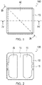
- FIG. 1 is a schematic upper face view of a light emitting device according to Embodiment 1.
- FIG. 2 is a schematic lower face view of the light emitting device of the embodiment.
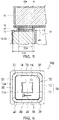
- FIG. 3 is a schematic cross-sectional view taken along line III-III in FIG. 1 .
- FIG. 4 is a schematic end face view only showing the cross section along line IV-IV in FIG. 1 .
- FIG. 5 is a schematic cross-sectional view enlarging a portion of the bonding member and the vicinity thereof in the light emitting device according to the embodiment.
- the light emitting device 100 shown in FIG. 3 includes a base 10 having an upper face 10a, a light emitting element 20 mounted on the upper face 10a, bonding members 30 disposed on the upper face 10a outward of the light emitting element 20, a light transmissive member 40 bonded to a portion of the upper face 10a by the bonding members 30, and a protective film 60 covering the upper face 10a of the base 10 and the light emitting element 20.
- the device has, between the upper face 10a of the base 10 and the lower face 40b of the light transmissive member 40, gaps 70 that allow the space in which the light emitting element 20 is mounted to be in communication with the outside of the light emitting device 100.
- the gaps 70 are defined by the upper face 10a of the base 10, the lower face 40b of the light transmissive member 40, and the bonding members 30.
- the protective film 60 continuously covers the light emitting element 20, the upper face 10a of the base 10, the lateral faces 30c of the bonding members 30, and the lower face 40b of the light transmissive member 40.
- the base 10 has a flat sheet-shaped base part 11, and a lateral wall part 12 disposed on the base part 11.
- the base part 11 and the lateral wall part 12 may be formed integrally, or as separate parts.
- the base part 11 and the lateral wall part 12 define a first recessed part.
- the first upper face 11a of the base part 11 is the bottom of the first recessed part.
- the light emitting element 20 is disposed on the first upper face 11a.
- the shape of the first upper face 11a when viewed from above is quadrangular, for example.
- the second upper face 12a which is the upper face of the lateral wall part 12, is positioned outward of the light emitting element 20 when viewed from above.
- the second upper face 12a is frame shaped having, for example, a quadrangular outline when viewed from above.
- Positive and negative first wires 14 are arranged on the first upper face 11a of the base 10.
- the light emitting element 20 is flip-chip mounted on the base 10. Specifically, using a light emitting element 20 having positive and negative electrodes on the same face, the positive and negative electrodes of the light emitting element 20 are electrically connected to the positive and negative first wires 14 of the base 10, respectively, via conductive members.
- conductive members for example, (i) eutectic solder using gold and tin, or tin, silver, and copper as main components, (ii) conductive paste containing silver, gold, or palladium, or (iii) bumps containing silver or gold can be used.
- the light emitting element 20 may be connected to the first wires 14 of the base 10 using wires (mounted face up).
- Second wires 15 are arranged on the lower face 10b of the base 10.
- the base part 11 of the base 10 has through holes, and internal wires (not shown) are disposed in the through holes.
- the first wires 14 and the second wires 15 are connected using the internal wires.
- the base 10 may or may not have second recessed parts 16 on the lower face 10b side.
- the second recessed parts 16 are provided from the lower face 10b to the outer lateral faces 10c of the base 10.
- the second wires 15 are also disposed on the outer lateral faces 16c of the base 10 that define the second recessed parts 16.
- a light transmissive member 40 is a member having light transmissivity that transmits at least the light from the light emitting element 20, transmitting at least 60%, preferably at least 90% of the emitted light from the light emitting element 20.
- the shape of the light transmissive member 40 is, for example, quadrangular when viewed from above.
- the light transmissive member 40 besides the flat sheet shape shown in FIG. 1 and FIG. 2 , may be such that the upper face and/or the lower face are/is spherical or aspherical lens shaped.
- a bonding member 30 bonds the second upper face 12a of the lateral wall part 12 of the base 10 and the light transmissive member 40. Because the lateral wall part 12 is disposed to surround the light emitting element 20 when viewed from above, the bonding member 30 is preferably disposed to surround the light emitting element 20 as well. The bonding member 30 is disposed on a portion of the second upper face 12a, not across the entire surface, of the base 10. In the portions in which the bonding members 30 are not disposed, as shown in FIG. 4 , there are gaps 70 between the second upper face 12a of the base 10 and the lower face of the light transmissive member 40 that are defined by the second upper face 12a of the base 10, the lower face 40b of the light transmissive member 40, and the bonding members 30.
- the gaps 70 allow the space in which the light emitting element 20 is disposed to be in communication with the outside of the light emitting device 100. In other words, the space in which the light emitting element 20 is disposed is not an airtight space in the light emitting device 100.
- a plurality of bonding members 30 are arranged.
- the bonding members 30 are disposed at the four corners of the second upper face 12a that is quadrangular when viewed from above.
- arranging them to have point symmetry about the center of the base 10 or line symmetry using the line connecting the centers of two opposing sides of the base 10 when viewed from above can increase the bonding quality between the base 10 and the light transmissive member 40.
- the bonding members 30 are arranged such that two pieces are present per side of the base 10.
- the bonding members 30 may be arranged such that one, three, or more pieces are present per side of the base 10.
- a bonding member 30 may be disposed in any position other than the four corners of the base 10, such as the center of a side of the base 10.
- a bonding member 30 may be disposed continuously over two or more sides. For example, one bonding member 30 can be disposed over three or four sides while leaving a gap at one location. In the case of disposing multiple bonding members 30, at least one bonding member 30 may be disposed over two or more sides of the base 10.
- one gap 70 is provided per side of the base 10. There may be a single gap 70, or multiple gaps 70 per side of the base 10. Two or more gaps 70 may be provided per side of the base 10.
- the height of a gap 70 (the thickness of the bonding member 30 between the second upper face 12a and the lower face 40b of the light transmissive member 40) can be set, for example, in a range of 1 ⁇ m to 100 ⁇ m.
- the height of a gap 70 is preferably set as 10 ⁇ m to 50 ⁇ m. In the case in which the first metal film 51 and the second metal film 52 described below are included, the height refers to the thickness of the bonding member 30 between the first metal film 51 and the second metal film 52.
- the percentage of the width of the bonding member 30 (30W in FIG. 5 ) of the base 10 in the width of the second upper face 12a (12W in FIG. 5 ) in the direction perpendicular to the sides of the base 10 is preferably set, for example, as at least 50%.
- the width of the second upper face 12a in the direction perpendicular to the sides of the base 10 can be set, for example, in a range of 0.3 mm to 0.7 mm.
- the width of the bonding member 30 in the direction perpendicular to the sides of the base 10 can be set, for example, in a range of 0.2 mm to 0.5 mm.
- a first metal film 51 may be disposed or not.
- the first metal film 51 is positioned between the bonding members 30 and the second upper face 12a of the base 10.
- the first metal film is quadrangular frame shaped when viewed from above, and the four corners are rounded.
- the bonding members 30 are disposed on the first metal film 51.
- a second metal film 52 may be disposed or not.
- the second metal film 52 is disposed between the bonding members 30 and the lower face 40b of the light transmissive member 40.
- the second meal film 52 opposes the second upper face 12a of the base 10.
- the second metal film 52 is frame-shaped and has a quadrangular outline with arc-shaped chamfers (indentations) at the corners in a plan view of the lower face 40b of the light transmissive member 40.
- the bonding members 30 are bonded to the second metal film 52.
- a protective film 60 is made of an inorganic material and continuously covers the base 10, the light emitting element 20, the bonding members 30, and the light transmissive member 40.
- the protective film 60 in the example shown in FIG. 3 and FIG. 4 covers the lower face 10b excluding the surfaces of the second wires 15 and the outer lateral faces 10c of the base 10, the lateral faces 30c of the bonding members 30, and the surfaces of the light transmissive member 40, making up the lower face and the lateral faces in part and the upper face among the outer surfaces of the light emitting device 100.
- the protective film 60 preferably also covers the downward facing face 16b of the base 10 that defines the second recessed part 16.
- the protective film 60 covers the inner lateral faces 10d of the lateral wall part 12 and the first upper face 11a of the base part 11 of the base 10 that define the first recessed part of the base 10. Moreover, under the light emitting element 20, the protective film 60 covers the lower face of the light emitting element 20, the lateral faces of the conductive members, and the first upper face 11a of the base 10 positioned under the light emitting element 20.
- the protective film 60 preferably covers the light emitting element 20, the second upper face 12a of the base 10, the lateral faces 30c of the bonding members 30 interposed between the second upper face 12a of the base 10 and the lower face of the light transmissive member 40, and the lower face 40b of the light transmissive member 40 without any gap, such as an opening or break.
- the protective film 60 covers the surfaces of the base 10 excluding the surfaces of the second wires 15, the surfaces of the light emitting element 20, the lateral faces 30c of the bonding members 30, and the surfaces of the light transmissive member 40.
- the light emitting device 100 may have a protective device, such as a Zener diode, or not.
- a protective device 80 is disposed on the first upper face 11a of the base 10.
- a base 10 is provided for mounting a light emitting element 20.
- the base 10 has a flat sheet shaped base part 11 and a lateral wall part 12 disposed on the base part 11.
- a light emitting element 20 is disposed on the first upper face 11a of the base part 11, and bonding members 30 are disposed on the second upper face 12a of the lateral wall part 12.
- the shape of the first upper face 11a of the base part 11 defined by the lateral wall part 12 when viewed from above is, for example, quadrangular.
- the base 10 includes an insulation base material, first wires 14, and second wires 15.
- the insulation base materials include ceramics, glass epoxy, and resins.
- ceramics a highly heat resistant and highly weather resistant material is preferably used.
- ceramics include alumina, aluminum nitride, mullite and the like.
- the first upper face 11a of the base 10 has first wires 14.
- the lower face 10b of the base 10 has second wires 15.
- the first wires 14 and the second wires 15 can be formed of any material known in the art.
- a metal such as copper, aluminum, gold, silver, or the like can be used.
- a light emitting element 20 is disposed on the first upper face 11a of the base part 11 of the base 10.
- a light emitting diode, laser diode, or the like can be used for the light emitting element 20.
- the peak emission wavelength for the light emitting element 20 there is no particular restriction for the peak emission wavelength for the light emitting element 20, and any peak emission wavelength can be suitably selected, for example, 250 nm to 600 nm.
- a light emitting diode that emits ultraviolet light can be used as a light source for sterilization or sanitization purposes.
- the peak emission wavelength for an ultraviolet light emitting element 20 is, for example, 400 nm at most. Because an ultraviolet light emitting element 20 tends to be readily degraded by moisture or the like, covering the element with a protective film 60 can notably improve the effect of reducing such degradation.
- the light emitting element 20 is preferably made of nitride semiconductor layers, such as In X Al Y Ga 1-X-Y N (0 ⁇ X, 0 ⁇ Y, X+Y ⁇ 1), for example.
- a light emitting element that emits light in the deep ultraviolet to ultraviolet wavelength range it preferably includes a nitride semiconductor layer containing at least Al.
- the light emitting element 20 includes semiconductor layers that include at least an emission layer, and positive and negative electrodes. In the light emitting element 20 according to this embodiment, the positive and negative electrodes are disposed on the same face.
- the light emitting element 20 can be flip-chip mounted on the base 10, thereby reducing the size of the light emitting device 100 as compared to the case in which the light emitting element 20 and the base 10 are electrically connected using wires.
- the face of the light emitting element that is opposite the face having the electrodes can be bonded to the first upper face 11a of the base 10 while electrically connecting the positive and negative electrodes of the light emitting element 20 to the positive and negative first wires 14 using wires, respectively.
- a light emitting element having one of the positive and negative electrodes on the upper face and the other electrode on the lower face can be used.
- the light emitting element 20 can have a substrate for growing a semiconductor layer in addition to the semiconductor layers and the electrodes described above.
- a substrate for growing a semiconductor layer in addition to the semiconductor layers and the electrodes described above.
- a substrate include an insulating substrate, such as sapphire, lithium niobate, or neodymium gallate, or a conductive substrate, such as SiC, ZnO, Si, GaAs, or the like.
- the substrate preferably has light transmissivity.
- the substrate may be removed by utilizing a laser lift-off technique or the like.
- the light emitting element 20 is disposed in the center of the first upper face 11a.
- the light emitting device 100 has one light emitting element 20.
- the light emitting device 100 may have multiple light emitting elements 20 arranged therein.
- the light emitting element 20 in a top view can have a quadrangular shape, for example.
- the length of a side of the light emitting element 20 when viewed from above is preferably in a range of 50 ⁇ m to 3,000 ⁇ m, for example, more preferably 300 ⁇ m to 2,000 ⁇ m.
- the top view shape of the light emitting element 20 may be another polygon, such as a triangle, hexagon, or the like.
- a bonding member 30 bonds the base 10 and the light transmissive member 40.
- the bonding member 30 include solder, low melting point glass, resins, and the like.
- solder include Au-Sn, Au-In, and the like.
- resins include silicone resins, epoxy resins, and the like.
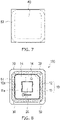
- FIG. 8 is a schematic top view showing another layout of the bonding members 30.
- multiple bonding members 30 are annularly arranged at certain intervals.
- the bonding members 30 are arranged in the regions excluding the four corners of the base 10.
- three or more bonding members 30 are arranged per side of the base 10. This can increase the bonding strength between the base 10 and the light transmissive member 40.
- a light transmissive member 40 has the function of transmitting the light from the light emitting element 20 disposed on the base 10 to be output from the light emitting device 100.
- the light transmissive member 40 preferably transmits at least 60%, more preferably at least 90% of the emitted light from the light emitting element 20.
- materials for use as the light transmissive member 40 include an inorganic material made of at least one selected from the group consisting of sapphire, borosilicate glass, quartz glass, calcium fluoride glass, aluminoborosilicate glass, oxynitride glass, and chalcogenide glass.
- the thickness of the light transmissive member 40 may be, for example, in a range of 0.1 mm to 7 mm.
- a protective film 60 has the function of protecting the light emitting element, the base, and the bonding members from dust and moisture.
- the protective film 60 has light transmissivity and insulation properties, and as shown in FIG. 2 , continuously covers at least the light emitting element 20, the upper face 10a of the base 10, and the lateral faces of the bonding members 30.
- the protective film 60 preferably covers substantially all surfaces of the light emitting device 100 except for the lower face. This can reduce the chance of allowing the protective film 60 to be separated from the surfaces of the light emitting device 100.
- the protective film 60 examples include inorganic materials, such as aluminum oxide, silicon dioxide, tantalum oxide, niobium oxide, titanium oxide, aluminum nitride, silicon nitride, and the like.
- the protective film 60 preferably is a film that contains aluminum oxide or silicon dioxide as a primary component.
- the protective film 60 can be of a single layer film of one material, or a multilayer film made of two or more different materials. Specifically, it is preferable to use a stack composed of a layer made of aluminum oxide as a primary component and a layer made of silicon dioxide as a primary component, or a stack in which these layers are repeatedly alternately stacked.
- the thickness of the protective film 60 is, for example, in a range of 3 nm to 250 nm.
- the thickness of the protective film 60 is preferably in a range of 40 nm to 150 nm. In the case of employing a multilayer film for the protective film 60, the total thickness of all layers is preferably set to fall within the ranges described
- the light emitting device 100 is such that the light emitting element 20, the base 10, and the lateral faces of the bonding members 30 are continuously covered by the protective film 60 to protect these members from the external factors, such as dust and moisture. Thus, deterioration attributable to oxidation or the like can be prevented. Accordingly, a highly reliable light emitting device 100 can be provided.
- FIG. 9A and FIG. 9B are schematic cross-sectional views explaining a method of manufacturing a light emitting device 100 of Embodiment 1.
- an intermediate body 110 which includes a base 10 having an upper face 10a, a light emitting element 20 mounted on the upper face 10a, a bonding member 30 disposed on the upper face 10a outward of the light emitting element 20, and a light transmissive member 40 bonded to a portion of the upper face 10a by the bonding member 30, is prepared.
- the intermediate body 110 has, between the upper face 10a of the base 10 and the lower face 40b of the light transmissive member 40, a gap 70 that allows the space in which the light emitting element 20 is mounted to be in communication with the outside of the intermediate body 110.
- the gap 70 is created by the bonding member 30 interposed between the upper face 10a of the base 10 and the lower face 40b of the light transmissive member 40.
- a light emitting element 20 is mounted on the first upper face 11a of the base 10.
- a bonding member 30 is disposed on a portion of the second upper face 12a outward of the light emitting element 20.
- an intermediate body 110 like that shown in FIG. 9A is obtained.
- Such an intermediate body 110 may be purchased, or prepared by following the intermediate body preparation process in part or whole.
- a protective film 60 that covers the upper face 10a of the base 10 and the light emitting element 20 is formed.
- the protective film 60 is preferably formed by atomic layer deposition (ALD). Forming the protective film 60 by atomic layer deposition can thinly form a dense protective film 60 across all surfaces that extend in different planar directions. Employing atomic layer deposition allows the gaseous raw material for forming the protective film 60 to be supplied through the gap created between the upper face 10a of the base 10 and the lower face 40b of the light transmissive member 40.
- ALD atomic layer deposition
- the protective film 60 can be formed to continuously cover at least the upper face 10a of the base 10, the light emitting element 20, and the lateral faces of the bonding member 30, but is preferably formed to substantially cover all surfaces of the light emitting device excluding the second wires 15 as shown in FIG. 9B .
- Examples of methods of selectively forming the protective film 60 as described above include one that forms a protective film 60 on all surfaces of the light emitting device 100 followed by removing the protective film 60 positioned on the second wires 15 by grinding or laser beam irradiation, one that uses a mask to cover the second wires 15 before forming a protective film 60, and the like.
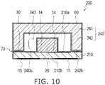
- FIG. 10 is a schematic end face view showing only a cross section of a light emitting device 200 according to Embodiment 2.
- the light emitting device 200 has a light emitting element 20 and a light transmissive member 240 on a flat sheet shaped base 210.
- the light transmissive member 240 has a flat sheet part 241, and a lateral wall part 242 positioned under the flat sheet part 241.
- the lower face 242b of the lateral wall part 242 is bonded to the base 210 via a bonding member 30.
- the flat sheet part 241 and the lateral wall part 242 of the light transmissive member 240 can be formed integrally.
- a light emitting element is positioned in the recessed part 243 defined by the flat sheet part 241 and the lateral wall part 242.
- the shape of the opening of the recessed part 243 is, for example, quadrangular.
- a gap 70 that allows the space in which the light emitting element 20 is mounted to be in communication with the outside of the light emitting device 100 is present between the base 210 and the lower face 242b of the light transmissive member 240.
- the gap 70 is defined by the upper face 10a of the base 10, the lower face 240b of the light transmissive member 240, and the bonding member 30.
- the protective film 60 covers the surfaces of the base 210, the surfaces of the light emitting element 20, the lateral faces of the bonding member 30, and the surfaces of the light transmissive member.
- the light emitting element 20, the base 210, and the lateral faces of the bonding member 30, which are continuously covered by the protective film 60 can be protected from dust and moisture to thereby prevent the deterioration attributable to oxidation and the like.
Landscapes
- Led Device Packages (AREA)
Abstract
Description
- The present disclosure relates to a light emitting device.
-
Japanese Patent Publication No. 2018-6456 -
-
FIG. 1 is a schematic upper face view of a light emitting device according toEmbodiment 1. -
FIG. 2 is a schematic lower face view of the light emitting device according toEmbodiment 1. -
FIG. 3 is a schematic cross-sectional view taken along line III-III inFIG. 1 . -
FIG. 4 is a schematic end face view, showing only the cross section along line IV-IV inFIG. 1 . -
FIG. 5 is a schematic cross-sectional view, enlarging a portion of the bonding member and the vicinity thereof in the light emitting device according toEmbodiment 1. -
FIG. 6 is a schematic upper face view showing the layout of bonding members. -
FIG. 7 is a schematic lower face view of a light transmissive member. -
FIG. 8 is a schematic upper face view showing another layout of bondingmembers 30. -
FIG. 9A is a schematic cross-sectional view explaining a method of manufacturing a light emitting device according toEmbodiment 1. -
FIG. 9B is a schematic cross-sectional view explaining a method of manufacturing a light emitting device according toEmbodiment 1. -
FIG. 10 is a schematic end face view showing only a cross section of a light emitting device according to Embodiment 2. - Certain embodiments of the present invention will be explained below with reference to the accompanying drawings. The embodiments explained below are provided for the purpose of giving shape to the technical ideas of the present invention, which do not limit the present invention unless otherwise specifically noted. The sizes of and positional relationships between the members shown in the drawings might be exaggerated for clarity of explanation.
- The present invention will be explained in detail below based on the drawings. In the explanation below, terms indicating specific directions or positions (e.g., "upper," "lower," or terms including these words) will be used as needed. These terms are used to make the embodiments in the drawings more easily understood, and the meaning of such terms does not restrict the technical scope of the present invention. The members or parts denoted by the same reference numerals are the same or equivalent members or parts.
- Furthermore, the embodiments described below are backlights shown as examples for the purpose of embodying the technical ideas of the present invention. However, the present invention is not limited to the examples described below. The dimensions, materials, shapes, and relative positions of the constituent elements described below are not meant to limit the scope of the invention unless otherwise specifically noted, but are intended to provide examples. The content described with reference to one embodiment or example is applicable to another embodiment or example. Moreover, the sizes of and positional relationships between the members shown in the drawings might be exaggerated for clarity of explanation.
-
FIG. 1 is a schematic upper face view of a light emitting device according toEmbodiment 1.FIG. 2 is a schematic lower face view of the light emitting device of the embodiment.FIG. 3 is a schematic cross-sectional view taken along line III-III inFIG. 1 .FIG. 4 is a schematic end face view only showing the cross section along line IV-IV inFIG. 1 .FIG. 5 is a schematic cross-sectional view enlarging a portion of the bonding member and the vicinity thereof in the light emitting device according to the embodiment. - The
light emitting device 100 shown inFIG. 3 includes abase 10 having anupper face 10a, alight emitting element 20 mounted on theupper face 10a, bondingmembers 30 disposed on theupper face 10a outward of thelight emitting element 20, a lighttransmissive member 40 bonded to a portion of theupper face 10a by thebonding members 30, and aprotective film 60 covering theupper face 10a of thebase 10 and thelight emitting element 20. The device has, between theupper face 10a of thebase 10 and thelower face 40b of the lighttransmissive member 40,gaps 70 that allow the space in which thelight emitting element 20 is mounted to be in communication with the outside of thelight emitting device 100. Thegaps 70 are defined by theupper face 10a of thebase 10, thelower face 40b of the lighttransmissive member 40, and thebonding members 30. Theprotective film 60 continuously covers thelight emitting element 20, theupper face 10a of thebase 10, thelateral faces 30c of thebonding members 30, and thelower face 40b of the lighttransmissive member 40. - In the example shown in
FIG. 1 , thebase 10 has a flat sheet-shaped base part 11, and alateral wall part 12 disposed on thebase part 11. Thebase part 11 and thelateral wall part 12 may be formed integrally, or as separate parts. Thebase part 11 and thelateral wall part 12 define a first recessed part. The firstupper face 11a of thebase part 11 is the bottom of the first recessed part. Thelight emitting element 20 is disposed on the firstupper face 11a. The shape of the firstupper face 11a when viewed from above is quadrangular, for example. As shown inFIG. 6 , the secondupper face 12a, which is the upper face of thelateral wall part 12, is positioned outward of thelight emitting element 20 when viewed from above. The secondupper face 12a is frame shaped having, for example, a quadrangular outline when viewed from above. - Positive and negative
first wires 14 are arranged on the firstupper face 11a of thebase 10. Thelight emitting element 20 is flip-chip mounted on thebase 10. Specifically, using alight emitting element 20 having positive and negative electrodes on the same face, the positive and negative electrodes of thelight emitting element 20 are electrically connected to the positive and negativefirst wires 14 of thebase 10, respectively, via conductive members. For the conductive members, for example, (i) eutectic solder using gold and tin, or tin, silver, and copper as main components, (ii) conductive paste containing silver, gold, or palladium, or (iii) bumps containing silver or gold can be used. Thelight emitting element 20 may be connected to thefirst wires 14 of thebase 10 using wires (mounted face up).Second wires 15 are arranged on thelower face 10b of thebase 10. Thebase part 11 of thebase 10 has through holes, and internal wires (not shown) are disposed in the through holes. Thefirst wires 14 and thesecond wires 15 are connected using the internal wires. Thebase 10 may or may not have secondrecessed parts 16 on thelower face 10b side. The second recessedparts 16 are provided from thelower face 10b to the outerlateral faces 10c of thebase 10. In the case in which secondrecessed parts 16 are provided, thesecond wires 15 are also disposed on the outerlateral faces 16c of thebase 10 that define the second recessedparts 16. When bonding thesecond wires 15 of thelight emitting device 100 to another mounting substrate or the like by using solder or the like, the solder can enter the secondrecessed part 16. This can electrically connect thesecond wires 15 in a more stable manner. - A light
transmissive member 40 is a member having light transmissivity that transmits at least the light from thelight emitting element 20, transmitting at least 60%, preferably at least 90% of the emitted light from thelight emitting element 20. The shape of the lighttransmissive member 40 is, for example, quadrangular when viewed from above. The lighttransmissive member 40, besides the flat sheet shape shown inFIG. 1 and FIG. 2 , may be such that the upper face and/or the lower face are/is spherical or aspherical lens shaped. - A bonding
member 30 bonds the secondupper face 12a of thelateral wall part 12 of thebase 10 and thelight transmissive member 40. Because thelateral wall part 12 is disposed to surround thelight emitting element 20 when viewed from above, the bondingmember 30 is preferably disposed to surround thelight emitting element 20 as well. The bondingmember 30 is disposed on a portion of the secondupper face 12a, not across the entire surface, of thebase 10. In the portions in which thebonding members 30 are not disposed, as shown inFIG. 4 , there aregaps 70 between the secondupper face 12a of thebase 10 and the lower face of thelight transmissive member 40 that are defined by the secondupper face 12a of thebase 10, thelower face 40b of thelight transmissive member 40, and thebonding members 30. Thegaps 70 allow the space in which thelight emitting element 20 is disposed to be in communication with the outside of thelight emitting device 100. In other words, the space in which thelight emitting element 20 is disposed is not an airtight space in thelight emitting device 100. - In the example shown in
FIG. 6 , a plurality ofbonding members 30 are arranged. Thebonding members 30 are disposed at the four corners of the secondupper face 12a that is quadrangular when viewed from above. In the case of arranging a plurality ofbonding member 30 as described above, arranging them to have point symmetry about the center of the base 10 or line symmetry using the line connecting the centers of two opposing sides of the base 10 when viewed from above can increase the bonding quality between the base 10 and thelight transmissive member 40. There is no particular restriction on the number and positions of thebonding members 30, as long as thegaps 70 secured after bonding thelight transmissive member 40 and the base 10 are large enough to allow a gaseous raw material to be supplied to the space in which thelight emitting element 20 is disposed during the process of forming aprotective film 60 described below. In the example shown inFIG. 6 , thebonding members 30 are arranged such that two pieces are present per side of thebase 10. Thebonding members 30 may be arranged such that one, three, or more pieces are present per side of thebase 10. A bondingmember 30 may be disposed in any position other than the four corners of thebase 10, such as the center of a side of thebase 10. A bondingmember 30 may be disposed continuously over two or more sides. For example, onebonding member 30 can be disposed over three or four sides while leaving a gap at one location. In the case of disposingmultiple bonding members 30, at least onebonding member 30 may be disposed over two or more sides of thebase 10. - In the example shown in
FIG. 6 , onegap 70 is provided per side of thebase 10. There may be asingle gap 70, ormultiple gaps 70 per side of thebase 10. Two ormore gaps 70 may be provided per side of thebase 10. The height of a gap 70 (the thickness of thebonding member 30 between the secondupper face 12a and thelower face 40b of the light transmissive member 40) can be set, for example, in a range of 1 µm to 100 µm. The height of agap 70 is preferably set as 10 µm to 50 µm. In the case in which thefirst metal film 51 and thesecond metal film 52 described below are included, the height refers to the thickness of thebonding member 30 between thefirst metal film 51 and thesecond metal film 52. There is no particular restriction on the width of agap 70, as long as it is large enough to allow a gaseous raw material to be supplied through thegap 70 into the space in which thelight emitting element 20 is disposed in the process of forming aprotective film 60 described below. The percentage of the width of the bonding member 30 (30W inFIG. 5 ) of the base 10 in the width of the secondupper face 12a (12W inFIG. 5 ) in the direction perpendicular to the sides of thebase 10 is preferably set, for example, as at least 50%. The width of the secondupper face 12a in the direction perpendicular to the sides of the base 10 can be set, for example, in a range of 0.3 mm to 0.7 mm. The width of thebonding member 30 in the direction perpendicular to the sides of the base 10 can be set, for example, in a range of 0.2 mm to 0.5 mm. - On the second
upper face 12a of thebase 10, afirst metal film 51 may be disposed or not. In the example shown inFIG. 6 , thefirst metal film 51 is positioned between thebonding members 30 and the secondupper face 12a of thebase 10. The first metal film is quadrangular frame shaped when viewed from above, and the four corners are rounded. In the case in which afirst metal film 51 is provided, thebonding members 30 are disposed on thefirst metal film 51. - In the peripheral portion of the
lower face 40b of thelight transmissive member 40, asecond metal film 52 may be disposed or not. In the example shown inFIG. 7 , thesecond metal film 52 is disposed between thebonding members 30 and thelower face 40b of thelight transmissive member 40. Thesecond meal film 52 opposes the secondupper face 12a of thebase 10. Thesecond metal film 52 is frame-shaped and has a quadrangular outline with arc-shaped chamfers (indentations) at the corners in a plan view of thelower face 40b of thelight transmissive member 40. In the case in which asecond metal film 52 is provided, thebonding members 30 are bonded to thesecond metal film 52. - A
protective film 60 is made of an inorganic material and continuously covers thebase 10, thelight emitting element 20, thebonding members 30, and thelight transmissive member 40. Theprotective film 60 in the example shown inFIG. 3 and FIG. 4 covers thelower face 10b excluding the surfaces of thesecond wires 15 and the outer lateral faces 10c of thebase 10, the lateral faces 30c of thebonding members 30, and the surfaces of thelight transmissive member 40, making up the lower face and the lateral faces in part and the upper face among the outer surfaces of thelight emitting device 100. In the case in which a second recessedpart 16 is provided, theprotective film 60 preferably also covers the downward facingface 16b of the base 10 that defines the second recessedpart 16. Furthermore, theprotective film 60 covers the inner lateral faces 10d of thelateral wall part 12 and the firstupper face 11a of thebase part 11 of the base 10 that define the first recessed part of thebase 10. Moreover, under thelight emitting element 20, theprotective film 60 covers the lower face of thelight emitting element 20, the lateral faces of the conductive members, and the firstupper face 11a of the base 10 positioned under thelight emitting element 20. Theprotective film 60 preferably covers thelight emitting element 20, the secondupper face 12a of thebase 10, the lateral faces 30c of thebonding members 30 interposed between the secondupper face 12a of thebase 10 and the lower face of thelight transmissive member 40, and thelower face 40b of thelight transmissive member 40 without any gap, such as an opening or break. In thelight emitting device 100 shown inFIG. 3 and FIG. 4 , theprotective film 60 covers the surfaces of the base 10 excluding the surfaces of thesecond wires 15, the surfaces of thelight emitting element 20, the lateral faces 30c of thebonding members 30, and the surfaces of thelight transmissive member 40. - The
light emitting device 100 may have a protective device, such as a Zener diode, or not. In the example shown inFIG. 6 , aprotective device 80 is disposed on the firstupper face 11a of thebase 10. - Each constituent element of the
light emitting device 100 will be explained below. - A
base 10 is provided for mounting alight emitting element 20. In the example shown inFIG. 3 , thebase 10 has a flat sheet shapedbase part 11 and alateral wall part 12 disposed on thebase part 11. Alight emitting element 20 is disposed on the firstupper face 11a of thebase part 11, andbonding members 30 are disposed on the secondupper face 12a of thelateral wall part 12. The shape of the firstupper face 11a of thebase part 11 defined by thelateral wall part 12 when viewed from above is, for example, quadrangular. - The
base 10 includes an insulation base material,first wires 14, andsecond wires 15. Examples of the insulation base materials include ceramics, glass epoxy, and resins. For ceramics, a highly heat resistant and highly weather resistant material is preferably used. Examples of such ceramics include alumina, aluminum nitride, mullite and the like. - The first
upper face 11a of thebase 10 hasfirst wires 14. Thelower face 10b of thebase 10 hassecond wires 15. Thefirst wires 14 and thesecond wires 15 can be formed of any material known in the art. For thefirst wires 14 and thesecond wires 15, for example, a metal, such as copper, aluminum, gold, silver, or the like can be used. - A
light emitting element 20 is disposed on the firstupper face 11a of thebase part 11 of thebase 10. For thelight emitting element 20, a light emitting diode, laser diode, or the like can be used. - There is no particular restriction for the peak emission wavelength for the
light emitting element 20, and any peak emission wavelength can be suitably selected, for example, 250 nm to 600 nm. For example, a light emitting diode that emits ultraviolet light can be used as a light source for sterilization or sanitization purposes. The peak emission wavelength for an ultravioletlight emitting element 20 is, for example, 400 nm at most. Because an ultravioletlight emitting element 20 tends to be readily degraded by moisture or the like, covering the element with aprotective film 60 can notably improve the effect of reducing such degradation. - The
light emitting element 20 is preferably made of nitride semiconductor layers, such as InXAlYGa1-X-YN (0≤X, 0≤Y, X+Y≤1), for example. In the case of using a light emitting element that emits light in the deep ultraviolet to ultraviolet wavelength range, it preferably includes a nitride semiconductor layer containing at least Al. Thelight emitting element 20 includes semiconductor layers that include at least an emission layer, and positive and negative electrodes. In thelight emitting element 20 according to this embodiment, the positive and negative electrodes are disposed on the same face. Accordingly, thelight emitting element 20 can be flip-chip mounted on thebase 10, thereby reducing the size of thelight emitting device 100 as compared to the case in which thelight emitting element 20 and the base 10 are electrically connected using wires. The face of the light emitting element that is opposite the face having the electrodes can be bonded to the firstupper face 11a of the base 10 while electrically connecting the positive and negative electrodes of thelight emitting element 20 to the positive and negativefirst wires 14 using wires, respectively. - Alternatively, a light emitting element having one of the positive and negative electrodes on the upper face and the other electrode on the lower face can be used.
- The
light emitting element 20 can have a substrate for growing a semiconductor layer in addition to the semiconductor layers and the electrodes described above. Examples of such a substrate include an insulating substrate, such as sapphire, lithium niobate, or neodymium gallate, or a conductive substrate, such as SiC, ZnO, Si, GaAs, or the like. The substrate preferably has light transmissivity. The substrate may be removed by utilizing a laser lift-off technique or the like. - In the example shown in
FIG. 6 , thelight emitting element 20 is disposed in the center of the firstupper face 11a. In the example shown inFIG. 6 , moreover, thelight emitting device 100 has onelight emitting element 20. Thelight emitting device 100 may have multiplelight emitting elements 20 arranged therein. Thelight emitting element 20 in a top view can have a quadrangular shape, for example. In this case, the length of a side of thelight emitting element 20 when viewed from above is preferably in a range of 50 µm to 3,000 µm, for example, more preferably 300 µm to 2,000 µm. The top view shape of thelight emitting element 20 may be another polygon, such as a triangle, hexagon, or the like. - A bonding
member 30 bonds thebase 10 and thelight transmissive member 40. The bondingmember 30, in the case in which thelight emitting device 100 includes afirst metal film 51 and asecond metal film 52, is disposed between thefirst metal film 51 and thesecond metal film 52. Examples of thebonding member 30 include solder, low melting point glass, resins, and the like. Examples of solder include Au-Sn, Au-In, and the like. Examples of resins include silicone resins, epoxy resins, and the like. -
FIG. 8 is a schematic top view showing another layout of thebonding members 30. In the example shown inFIG. 8 ,multiple bonding members 30 are annularly arranged at certain intervals. Thebonding members 30 are arranged in the regions excluding the four corners of thebase 10. In the example shown inFIG. 8 , three ormore bonding members 30 are arranged per side of thebase 10. This can increase the bonding strength between the base 10 and thelight transmissive member 40. - A
light transmissive member 40 has the function of transmitting the light from thelight emitting element 20 disposed on the base 10 to be output from thelight emitting device 100. Thelight transmissive member 40 preferably transmits at least 60%, more preferably at least 90% of the emitted light from thelight emitting element 20. Examples of materials for use as thelight transmissive member 40 include an inorganic material made of at least one selected from the group consisting of sapphire, borosilicate glass, quartz glass, calcium fluoride glass, aluminoborosilicate glass, oxynitride glass, and chalcogenide glass. The thickness of thelight transmissive member 40 may be, for example, in a range of 0.1 mm to 7 mm. - A
protective film 60 has the function of protecting the light emitting element, the base, and the bonding members from dust and moisture. Theprotective film 60 has light transmissivity and insulation properties, and as shown inFIG. 2 , continuously covers at least thelight emitting element 20, theupper face 10a of thebase 10, and the lateral faces of thebonding members 30. As shown inFIG. 2 , theprotective film 60 preferably covers substantially all surfaces of thelight emitting device 100 except for the lower face. This can reduce the chance of allowing theprotective film 60 to be separated from the surfaces of thelight emitting device 100. - Examples of materials for the
protective film 60 include inorganic materials, such as aluminum oxide, silicon dioxide, tantalum oxide, niobium oxide, titanium oxide, aluminum nitride, silicon nitride, and the like. Theprotective film 60 preferably is a film that contains aluminum oxide or silicon dioxide as a primary component. Theprotective film 60 can be of a single layer film of one material, or a multilayer film made of two or more different materials. Specifically, it is preferable to use a stack composed of a layer made of aluminum oxide as a primary component and a layer made of silicon dioxide as a primary component, or a stack in which these layers are repeatedly alternately stacked. The thickness of theprotective film 60 is, for example, in a range of 3 nm to 250 nm. The thickness of theprotective film 60 is preferably in a range of 40 nm to 150 nm. In the case of employing a multilayer film for theprotective film 60, the total thickness of all layers is preferably set to fall within the ranges described above. - The
light emitting device 100 according to this embodiment is such that thelight emitting element 20, thebase 10, and the lateral faces of thebonding members 30 are continuously covered by theprotective film 60 to protect these members from the external factors, such as dust and moisture. Thus, deterioration attributable to oxidation or the like can be prevented. Accordingly, a highly reliable lightemitting device 100 can be provided. -
FIG. 9A and FIG. 9B are schematic cross-sectional views explaining a method of manufacturing alight emitting device 100 ofEmbodiment 1. - As shown in
FIG. 9A , anintermediate body 110, which includes a base 10 having anupper face 10a, alight emitting element 20 mounted on theupper face 10a, abonding member 30 disposed on theupper face 10a outward of thelight emitting element 20, and alight transmissive member 40 bonded to a portion of theupper face 10a by the bondingmember 30, is prepared. Theintermediate body 110 has, between theupper face 10a of thebase 10 and thelower face 40b of thelight transmissive member 40, agap 70 that allows the space in which thelight emitting element 20 is mounted to be in communication with the outside of theintermediate body 110. Thegap 70 is created by the bondingmember 30 interposed between theupper face 10a of thebase 10 and thelower face 40b of thelight transmissive member 40. - One example of the method of manufacturing such an
intermediate body 110 will be explained. First, alight emitting element 20 is mounted on the firstupper face 11a of thebase 10. A bondingmember 30 is disposed on a portion of the secondupper face 12a outward of thelight emitting element 20. Subsequently, by bonding the portion of the secondupper face 12a and thelight transmissive member 40 using thebonding member 30, anintermediate body 110 like that shown inFIG. 9A is obtained. Such anintermediate body 110 may be purchased, or prepared by following the intermediate body preparation process in part or whole. - Next, as shown in
FIG. 9B , aprotective film 60 that covers theupper face 10a of thebase 10 and thelight emitting element 20 is formed. - The
protective film 60 is preferably formed by atomic layer deposition (ALD). Forming theprotective film 60 by atomic layer deposition can thinly form a denseprotective film 60 across all surfaces that extend in different planar directions. Employing atomic layer deposition allows the gaseous raw material for forming theprotective film 60 to be supplied through the gap created between theupper face 10a of thebase 10 and thelower face 40b of thelight transmissive member 40. - The
protective film 60 can be formed to continuously cover at least theupper face 10a of thebase 10, thelight emitting element 20, and the lateral faces of thebonding member 30, but is preferably formed to substantially cover all surfaces of the light emitting device excluding thesecond wires 15 as shown inFIG. 9B . Examples of methods of selectively forming theprotective film 60 as described above include one that forms aprotective film 60 on all surfaces of thelight emitting device 100 followed by removing theprotective film 60 positioned on thesecond wires 15 by grinding or laser beam irradiation, one that uses a mask to cover thesecond wires 15 before forming aprotective film 60, and the like. -
FIG. 10 is a schematic end face view showing only a cross section of alight emitting device 200 according to Embodiment 2. - The
light emitting device 200 has alight emitting element 20 and alight transmissive member 240 on a flat sheet shapedbase 210. Thelight transmissive member 240 has aflat sheet part 241, and alateral wall part 242 positioned under theflat sheet part 241. Thelower face 242b of thelateral wall part 242 is bonded to thebase 210 via abonding member 30. Theflat sheet part 241 and thelateral wall part 242 of thelight transmissive member 240 can be formed integrally. A light emitting element is positioned in the recessedpart 243 defined by theflat sheet part 241 and thelateral wall part 242. The shape of the opening of the recessedpart 243 is, for example, quadrangular. Agap 70 that allows the space in which thelight emitting element 20 is mounted to be in communication with the outside of thelight emitting device 100 is present between the base 210 and thelower face 242b of thelight transmissive member 240. Thegap 70 is defined by theupper face 10a of thebase 10, thelower face 240b of thelight transmissive member 240, and thebonding member 30. Theprotective film 60 covers the surfaces of thebase 210, the surfaces of thelight emitting element 20, the lateral faces of thebonding member 30, and the surfaces of the light transmissive member. In thelight emitting device 200 shown inFIG. 10 , thelight emitting element 20, thebase 210, and the lateral faces of thebonding member 30, which are continuously covered by theprotective film 60, can be protected from dust and moisture to thereby prevent the deterioration attributable to oxidation and the like.
Claims (7)
- A light emitting device (100) characterized by comprising:a base (10) having an upper face;a light emitting element (20) mounted on the upper face of the base;one or more bonding members (30) disposed on the upper face of the base outward of the light emitting element;a light transmissive member (40) bonded to a portion of the upper face of the base by the one or more bonding members; anda protective film (60) that continuously covers the light emitting element, the upper face of the base, lateral faces of the one or more bonding members, and a lower face of the light transmissive member; wherein:
a gap (70) is located between the upper face of the base and the lower face of the light transmissive member and configured to allow a space in which the light emitting element is mounted to communicate with an outside of the light emitting device, wherein the gap is defined by the upper face of the base, the lower face of the light transmissive member, and the one or more bonding members. - The light emitting device (100) according to claim 1, characterized in that the one or more bonding members (30) comprise a plurality of bonding members.
- The light emitting device (100) according to claim 1 or 2 characterized by further comprising a first metal film (51) between the one or more bonding members (30) and the upper face of the base, wherein the protective film (60) continuously covers the one or more bonding members, the first metal film, and the base (10).
- The light emitting device (100) according to any of claims 1 to 3 characterized by further comprising a second metal film (52) between the one or more bonding members (30) and the lower face of the light transmissive member (40), wherein the protective film (60) continuously covers the one or more bonding members, the second metal film, and the lower face of the light transmissive member.
- The light emitting device (100) according to any of claims 1 to 4, characterized in that:the base (10) has a flat sheet shaped base part (11) and a lateral wall part (12) disposed on the base part (10), the base part and the lateral wall part defining a recessed part ();the light emitting element (20) is disposed in the recessed part; andthe protective film covers (60) inner lateral faces of the lateral wall part and an upper face of the base part that define the recessed part.
- The light emitting device (100) according to any of claims 1 to 5, characterized in that the protective film (60) is made of an inorganic material.
- The light emitting device (100) according to any of claims 1 to 6, characterized in that the protective film (60) is a multilayer film.
Applications Claiming Priority (1)
| Application Number | Priority Date | Filing Date | Title |
|---|---|---|---|
| JP2021071348A JP7387978B2 (en) | 2021-04-20 | 2021-04-20 | light emitting device |
Publications (2)
| Publication Number | Publication Date |
|---|---|
| EP4080590A1 true EP4080590A1 (en) | 2022-10-26 |
| EP4080590B1 EP4080590B1 (en) | 2024-02-28 |
Family
ID=81344371
Family Applications (1)
| Application Number | Title | Priority Date | Filing Date |
|---|---|---|---|
| EP22168969.8A Active EP4080590B1 (en) | 2021-04-20 | 2022-04-20 | Light emitting device |
Country Status (4)
| Country | Link |
|---|---|
| US (1) | US12243972B2 (en) |
| EP (1) | EP4080590B1 (en) |
| JP (1) | JP7387978B2 (en) |
| CN (1) | CN115224174B (en) |
Families Citing this family (1)
| Publication number | Priority date | Publication date | Assignee | Title |
|---|---|---|---|---|
| EP4603916A1 (en) | 2022-10-14 | 2025-08-20 | Canon Kabushiki Kaisha | Toner cartridge and image-forming device |
Citations (3)
| Publication number | Priority date | Publication date | Assignee | Title |
|---|---|---|---|---|
| JP2018006456A (en) | 2016-06-29 | 2018-01-11 | 日本電気硝子株式会社 | Airtight package and manufacturing method thereof |
| EP3664166A1 (en) * | 2018-12-05 | 2020-06-10 | Lite-On Opto Technology (Changzhou) Co., Ltd. | Light emitting package structure and method of manufacturing the same |
| US20200343425A1 (en) * | 2017-12-27 | 2020-10-29 | Innolux Corporation | Display device |
Family Cites Families (30)
| Publication number | Priority date | Publication date | Assignee | Title |
|---|---|---|---|---|
| JPH0548361U (en) | 1991-11-29 | 1993-06-25 | ホーヤ株式会社 | Photoelectric conversion device |
| JP3045913B2 (en) * | 1993-12-24 | 2000-05-29 | 松下電子工業株式会社 | Semiconductor laser device and method of manufacturing the same |
| JP2005175039A (en) | 2003-12-09 | 2005-06-30 | Kenichiro Miyahara | Light emitting element mounting substrate and light emitting element |
| US7348193B2 (en) | 2005-06-30 | 2008-03-25 | Corning Incorporated | Hermetic seals for micro-electromechanical system devices |
| JP2009016383A (en) | 2007-06-29 | 2009-01-22 | Fujitsu Ltd | Packaged device and packaged device manufacturing method |
| DE102008038748B4 (en) | 2008-08-12 | 2022-08-04 | OSRAM Opto Semiconductors Gesellschaft mit beschränkter Haftung | Surface-mount optoelectronic semiconductor component |
| US20100167002A1 (en) | 2008-12-30 | 2010-07-01 | Vitex Systems, Inc. | Method for encapsulating environmentally sensitive devices |
| WO2011013581A1 (en) * | 2009-07-30 | 2011-02-03 | 日亜化学工業株式会社 | Light emitting device and method for manufacturing same |
| DE102009058796A1 (en) | 2009-12-18 | 2011-06-22 | OSRAM Opto Semiconductors GmbH, 93055 | Optoelectronic component and method for producing an optoelectronic component |
| JP2012060039A (en) | 2010-09-13 | 2012-03-22 | Sanyo Electric Co Ltd | Semiconductor laser device and optical device |
| JP5864089B2 (en) | 2010-08-25 | 2016-02-17 | 日亜化学工業株式会社 | Method for manufacturing light emitting device |
| US9240524B2 (en) | 2012-03-05 | 2016-01-19 | Seoul Viosys Co., Ltd. | Light-emitting device and method of manufacturing the same |
| JP6128938B2 (en) | 2013-04-26 | 2017-05-17 | 株式会社トクヤマ | Semiconductor light emitting device package |
| JP2015018873A (en) | 2013-07-09 | 2015-01-29 | 日機装株式会社 | Semiconductor module |
| JP6232792B2 (en) | 2013-07-17 | 2017-11-22 | 日亜化学工業株式会社 | Light emitting device |
| JP6602622B2 (en) | 2014-09-25 | 2019-11-06 | 山村フォトニクス株式会社 | Optical device apparatus and protective cover for covering optical device |
| EP3038173B1 (en) | 2014-12-23 | 2019-05-22 | LG Innotek Co., Ltd. | Light emitting device |
| JP6557970B2 (en) | 2014-12-26 | 2019-08-14 | 日亜化学工業株式会社 | Light emitting device |
| KR102305234B1 (en) | 2015-01-28 | 2021-09-29 | 쑤저우 레킨 세미컨덕터 컴퍼니 리미티드 | Lighting source unit |
| JP6327232B2 (en) | 2015-10-30 | 2018-05-23 | 日亜化学工業株式会社 | LIGHT EMITTING DEVICE AND LIGHT EMITTING MODULE MANUFACTURING METHOD |
| CN106848031A (en) | 2015-12-04 | 2017-06-13 | 财团法人工业技术研究院 | Packaging structure of ultraviolet light emitting diode |
| CN107195751B (en) | 2016-03-14 | 2020-01-14 | 光宝光电(常州)有限公司 | Light emitting diode packaging structure |
| TW201742271A (en) | 2016-05-23 | 2017-12-01 | 聯京光電股份有限公司 | Ultraviolet light emitting diode package structure |
| TWI686966B (en) | 2016-06-06 | 2020-03-01 | 行政院原子能委員會核能研究所 | Packaging structure of ultraviolet light emitting diode element |
| JP6920602B2 (en) | 2016-09-28 | 2021-08-18 | 日亜化学工業株式会社 | Light emitting device and manufacturing method of light emitting device |
| CN110476261A (en) | 2017-04-06 | 2019-11-19 | 日本碍子株式会社 | Optical component and the transparent body |
| JP6939690B2 (en) | 2018-04-23 | 2021-09-22 | セイコーエプソン株式会社 | Light source device and projector |
| JP6848931B2 (en) | 2018-04-23 | 2021-03-24 | セイコーエプソン株式会社 | Light source device and projector |
| JP7152666B2 (en) * | 2019-03-08 | 2022-10-13 | 日亜化学工業株式会社 | Light-emitting device and manufacturing method thereof |
| EP4160704B1 (en) * | 2021-09-29 | 2024-12-18 | Nichia Corporation | Light emitting device and method of manufacturing light emitting device |
-
2021
- 2021-04-20 JP JP2021071348A patent/JP7387978B2/en active Active
-
2022
- 2022-04-19 CN CN202210408724.4A patent/CN115224174B/en active Active
- 2022-04-19 US US17/724,139 patent/US12243972B2/en active Active
- 2022-04-20 EP EP22168969.8A patent/EP4080590B1/en active Active
Patent Citations (3)
| Publication number | Priority date | Publication date | Assignee | Title |
|---|---|---|---|---|
| JP2018006456A (en) | 2016-06-29 | 2018-01-11 | 日本電気硝子株式会社 | Airtight package and manufacturing method thereof |
| US20200343425A1 (en) * | 2017-12-27 | 2020-10-29 | Innolux Corporation | Display device |
| EP3664166A1 (en) * | 2018-12-05 | 2020-06-10 | Lite-On Opto Technology (Changzhou) Co., Ltd. | Light emitting package structure and method of manufacturing the same |
Also Published As
| Publication number | Publication date |
|---|---|
| US20220336722A1 (en) | 2022-10-20 |
| JP2022165826A (en) | 2022-11-01 |
| US12243972B2 (en) | 2025-03-04 |
| CN115224174A (en) | 2022-10-21 |
| EP4080590B1 (en) | 2024-02-28 |
| CN115224174B (en) | 2026-01-09 |
| JP7387978B2 (en) | 2023-11-29 |
Similar Documents
| Publication | Publication Date | Title |
|---|---|---|
| JP7054025B2 (en) | Light emitting device | |
| US11710810B2 (en) | Light-emitting device | |
| CN107968147B (en) | light-emitting device | |
| KR102236796B1 (en) | Light emitting device | |
| JP6175952B2 (en) | Light emitting device | |
| JP6773162B2 (en) | Light emitting device | |
| US10629790B2 (en) | Light-emitting device | |
| EP3067944B1 (en) | Semiconductor light emitting device and method of manufacturing the same | |
| EP2669962B1 (en) | Semiconductor light meitting device | |
| US20180151781A1 (en) | Light emitting device package structure and manufacturing method thereof | |
| KR102447343B1 (en) | light emitting device | |
| US10224468B2 (en) | Method of manufacturing light emitting device | |
| EP4080590B1 (en) | Light emitting device | |
| US10847693B2 (en) | Light emitting device and lead frame with resin | |
| US20250056938A1 (en) | Semiconductor light-emitting apparatus | |
| HK1190822A (en) | Semiconductor light emitting device and method for manufacturing same |
Legal Events
| Date | Code | Title | Description |
|---|---|---|---|
| PUAI | Public reference made under article 153(3) epc to a published international application that has entered the european phase |
Free format text: ORIGINAL CODE: 0009012 |
|
| STAA | Information on the status of an ep patent application or granted ep patent |
Free format text: STATUS: REQUEST FOR EXAMINATION WAS MADE |
|
| 17P | Request for examination filed |
Effective date: 20220420 |
|
| AK | Designated contracting states |
Kind code of ref document: A1 Designated state(s): AL AT BE BG CH CY CZ DE DK EE ES FI FR GB GR HR HU IE IS IT LI LT LU LV MC MK MT NL NO PL PT RO RS SE SI SK SM TR |
|
| P01 | Opt-out of the competence of the unified patent court (upc) registered |
Effective date: 20230522 |
|
| GRAP | Despatch of communication of intention to grant a patent |
Free format text: ORIGINAL CODE: EPIDOSNIGR1 |
|
| STAA | Information on the status of an ep patent application or granted ep patent |
Free format text: STATUS: GRANT OF PATENT IS INTENDED |
|
| INTG | Intention to grant announced |
Effective date: 20230919 |
|
| GRAS | Grant fee paid |
Free format text: ORIGINAL CODE: EPIDOSNIGR3 |
|
| GRAA | (expected) grant |
Free format text: ORIGINAL CODE: 0009210 |
|
| STAA | Information on the status of an ep patent application or granted ep patent |
Free format text: STATUS: THE PATENT HAS BEEN GRANTED |
|
| AK | Designated contracting states |
Kind code of ref document: B1 Designated state(s): AL AT BE BG CH CY CZ DE DK EE ES FI FR GB GR HR HU IE IS IT LI LT LU LV MC MK MT NL NO PL PT RO RS SE SI SK SM TR |
|
| REG | Reference to a national code |
Ref country code: GB Ref legal event code: FG4D |
|
| REG | Reference to a national code |
Ref country code: CH Ref legal event code: EP |
|
| REG | Reference to a national code |
Ref country code: DE Ref legal event code: R096 Ref document number: 602022002105 Country of ref document: DE |
|
| REG | Reference to a national code |
Ref country code: IE Ref legal event code: FG4D |
|
| REG | Reference to a national code |
Ref country code: LT Ref legal event code: MG9D |
|
| PG25 | Lapsed in a contracting state [announced via postgrant information from national office to epo] |
Ref country code: IS Free format text: LAPSE BECAUSE OF FAILURE TO SUBMIT A TRANSLATION OF THE DESCRIPTION OR TO PAY THE FEE WITHIN THE PRESCRIBED TIME-LIMIT Effective date: 20240628 |
|
| REG | Reference to a national code |
Ref country code: NL Ref legal event code: MP Effective date: 20240228 |
|
| PG25 | Lapsed in a contracting state [announced via postgrant information from national office to epo] |
Ref country code: LT Free format text: LAPSE BECAUSE OF FAILURE TO SUBMIT A TRANSLATION OF THE DESCRIPTION OR TO PAY THE FEE WITHIN THE PRESCRIBED TIME-LIMIT Effective date: 20240228 |
|
| PG25 | Lapsed in a contracting state [announced via postgrant information from national office to epo] |
Ref country code: GR Free format text: LAPSE BECAUSE OF FAILURE TO SUBMIT A TRANSLATION OF THE DESCRIPTION OR TO PAY THE FEE WITHIN THE PRESCRIBED TIME-LIMIT Effective date: 20240529 |
|
| PG25 | Lapsed in a contracting state [announced via postgrant information from national office to epo] |
Ref country code: HR Free format text: LAPSE BECAUSE OF FAILURE TO SUBMIT A TRANSLATION OF THE DESCRIPTION OR TO PAY THE FEE WITHIN THE PRESCRIBED TIME-LIMIT Effective date: 20240228 Ref country code: RS Free format text: LAPSE BECAUSE OF FAILURE TO SUBMIT A TRANSLATION OF THE DESCRIPTION OR TO PAY THE FEE WITHIN THE PRESCRIBED TIME-LIMIT Effective date: 20240528 Ref country code: NL Free format text: LAPSE BECAUSE OF FAILURE TO SUBMIT A TRANSLATION OF THE DESCRIPTION OR TO PAY THE FEE WITHIN THE PRESCRIBED TIME-LIMIT Effective date: 20240228 |
|
| PG25 | Lapsed in a contracting state [announced via postgrant information from national office to epo] |
Ref country code: ES Free format text: LAPSE BECAUSE OF FAILURE TO SUBMIT A TRANSLATION OF THE DESCRIPTION OR TO PAY THE FEE WITHIN THE PRESCRIBED TIME-LIMIT Effective date: 20240228 |
|
| PG25 | Lapsed in a contracting state [announced via postgrant information from national office to epo] |
Ref country code: RS Free format text: LAPSE BECAUSE OF FAILURE TO SUBMIT A TRANSLATION OF THE DESCRIPTION OR TO PAY THE FEE WITHIN THE PRESCRIBED TIME-LIMIT Effective date: 20240528 Ref country code: NO Free format text: LAPSE BECAUSE OF FAILURE TO SUBMIT A TRANSLATION OF THE DESCRIPTION OR TO PAY THE FEE WITHIN THE PRESCRIBED TIME-LIMIT Effective date: 20240528 Ref country code: NL Free format text: LAPSE BECAUSE OF FAILURE TO SUBMIT A TRANSLATION OF THE DESCRIPTION OR TO PAY THE FEE WITHIN THE PRESCRIBED TIME-LIMIT Effective date: 20240228 Ref country code: LT Free format text: LAPSE BECAUSE OF FAILURE TO SUBMIT A TRANSLATION OF THE DESCRIPTION OR TO PAY THE FEE WITHIN THE PRESCRIBED TIME-LIMIT Effective date: 20240228 Ref country code: IS Free format text: LAPSE BECAUSE OF FAILURE TO SUBMIT A TRANSLATION OF THE DESCRIPTION OR TO PAY THE FEE WITHIN THE PRESCRIBED TIME-LIMIT Effective date: 20240628 Ref country code: HR Free format text: LAPSE BECAUSE OF FAILURE TO SUBMIT A TRANSLATION OF THE DESCRIPTION OR TO PAY THE FEE WITHIN THE PRESCRIBED TIME-LIMIT Effective date: 20240228 Ref country code: GR Free format text: LAPSE BECAUSE OF FAILURE TO SUBMIT A TRANSLATION OF THE DESCRIPTION OR TO PAY THE FEE WITHIN THE PRESCRIBED TIME-LIMIT Effective date: 20240529 Ref country code: FI Free format text: LAPSE BECAUSE OF FAILURE TO SUBMIT A TRANSLATION OF THE DESCRIPTION OR TO PAY THE FEE WITHIN THE PRESCRIBED TIME-LIMIT Effective date: 20240228 Ref country code: ES Free format text: LAPSE BECAUSE OF FAILURE TO SUBMIT A TRANSLATION OF THE DESCRIPTION OR TO PAY THE FEE WITHIN THE PRESCRIBED TIME-LIMIT Effective date: 20240228 Ref country code: BG Free format text: LAPSE BECAUSE OF FAILURE TO SUBMIT A TRANSLATION OF THE DESCRIPTION OR TO PAY THE FEE WITHIN THE PRESCRIBED TIME-LIMIT Effective date: 20240228 |
|
| PG25 | Lapsed in a contracting state [announced via postgrant information from national office to epo] |
Ref country code: PL Free format text: LAPSE BECAUSE OF FAILURE TO SUBMIT A TRANSLATION OF THE DESCRIPTION OR TO PAY THE FEE WITHIN THE PRESCRIBED TIME-LIMIT Effective date: 20240228 Ref country code: PT Free format text: LAPSE BECAUSE OF FAILURE TO SUBMIT A TRANSLATION OF THE DESCRIPTION OR TO PAY THE FEE WITHIN THE PRESCRIBED TIME-LIMIT Effective date: 20240628 |
|
| REG | Reference to a national code |
Ref country code: AT Ref legal event code: MK05 Ref document number: 1662065 Country of ref document: AT Kind code of ref document: T Effective date: 20240228 |
|
| PG25 | Lapsed in a contracting state [announced via postgrant information from national office to epo] |
Ref country code: SE Free format text: LAPSE BECAUSE OF FAILURE TO SUBMIT A TRANSLATION OF THE DESCRIPTION OR TO PAY THE FEE WITHIN THE PRESCRIBED TIME-LIMIT Effective date: 20240228 Ref country code: PT Free format text: LAPSE BECAUSE OF FAILURE TO SUBMIT A TRANSLATION OF THE DESCRIPTION OR TO PAY THE FEE WITHIN THE PRESCRIBED TIME-LIMIT Effective date: 20240628 Ref country code: PL Free format text: LAPSE BECAUSE OF FAILURE TO SUBMIT A TRANSLATION OF THE DESCRIPTION OR TO PAY THE FEE WITHIN THE PRESCRIBED TIME-LIMIT Effective date: 20240228 Ref country code: LV Free format text: LAPSE BECAUSE OF FAILURE TO SUBMIT A TRANSLATION OF THE DESCRIPTION OR TO PAY THE FEE WITHIN THE PRESCRIBED TIME-LIMIT Effective date: 20240228 |
|
| PG25 | Lapsed in a contracting state [announced via postgrant information from national office to epo] |
Ref country code: DK Free format text: LAPSE BECAUSE OF FAILURE TO SUBMIT A TRANSLATION OF THE DESCRIPTION OR TO PAY THE FEE WITHIN THE PRESCRIBED TIME-LIMIT Effective date: 20240228 |
|
| PG25 | Lapsed in a contracting state [announced via postgrant information from national office to epo] |
Ref country code: SM Free format text: LAPSE BECAUSE OF FAILURE TO SUBMIT A TRANSLATION OF THE DESCRIPTION OR TO PAY THE FEE WITHIN THE PRESCRIBED TIME-LIMIT Effective date: 20240228 |
|
| PG25 | Lapsed in a contracting state [announced via postgrant information from national office to epo] |
Ref country code: EE Free format text: LAPSE BECAUSE OF FAILURE TO SUBMIT A TRANSLATION OF THE DESCRIPTION OR TO PAY THE FEE WITHIN THE PRESCRIBED TIME-LIMIT Effective date: 20240228 Ref country code: CZ Free format text: LAPSE BECAUSE OF FAILURE TO SUBMIT A TRANSLATION OF THE DESCRIPTION OR TO PAY THE FEE WITHIN THE PRESCRIBED TIME-LIMIT Effective date: 20240228 |
|
| PG25 | Lapsed in a contracting state [announced via postgrant information from national office to epo] |
Ref country code: AT Free format text: LAPSE BECAUSE OF FAILURE TO SUBMIT A TRANSLATION OF THE DESCRIPTION OR TO PAY THE FEE WITHIN THE PRESCRIBED TIME-LIMIT Effective date: 20240228 |
|
| PG25 | Lapsed in a contracting state [announced via postgrant information from national office to epo] |
Ref country code: SK Free format text: LAPSE BECAUSE OF FAILURE TO SUBMIT A TRANSLATION OF THE DESCRIPTION OR TO PAY THE FEE WITHIN THE PRESCRIBED TIME-LIMIT Effective date: 20240228 |
|
| PG25 | Lapsed in a contracting state [announced via postgrant information from national office to epo] |
Ref country code: SM Free format text: LAPSE BECAUSE OF FAILURE TO SUBMIT A TRANSLATION OF THE DESCRIPTION OR TO PAY THE FEE WITHIN THE PRESCRIBED TIME-LIMIT Effective date: 20240228 Ref country code: SK Free format text: LAPSE BECAUSE OF FAILURE TO SUBMIT A TRANSLATION OF THE DESCRIPTION OR TO PAY THE FEE WITHIN THE PRESCRIBED TIME-LIMIT Effective date: 20240228 Ref country code: RO Free format text: LAPSE BECAUSE OF FAILURE TO SUBMIT A TRANSLATION OF THE DESCRIPTION OR TO PAY THE FEE WITHIN THE PRESCRIBED TIME-LIMIT Effective date: 20240228 Ref country code: EE Free format text: LAPSE BECAUSE OF FAILURE TO SUBMIT A TRANSLATION OF THE DESCRIPTION OR TO PAY THE FEE WITHIN THE PRESCRIBED TIME-LIMIT Effective date: 20240228 Ref country code: DK Free format text: LAPSE BECAUSE OF FAILURE TO SUBMIT A TRANSLATION OF THE DESCRIPTION OR TO PAY THE FEE WITHIN THE PRESCRIBED TIME-LIMIT Effective date: 20240228 Ref country code: CZ Free format text: LAPSE BECAUSE OF FAILURE TO SUBMIT A TRANSLATION OF THE DESCRIPTION OR TO PAY THE FEE WITHIN THE PRESCRIBED TIME-LIMIT Effective date: 20240228 Ref country code: AT Free format text: LAPSE BECAUSE OF FAILURE TO SUBMIT A TRANSLATION OF THE DESCRIPTION OR TO PAY THE FEE WITHIN THE PRESCRIBED TIME-LIMIT Effective date: 20240228 |
|
| PG25 | Lapsed in a contracting state [announced via postgrant information from national office to epo] |
Ref country code: MC Free format text: LAPSE BECAUSE OF FAILURE TO SUBMIT A TRANSLATION OF THE DESCRIPTION OR TO PAY THE FEE WITHIN THE PRESCRIBED TIME-LIMIT Effective date: 20240228 |
|
| REG | Reference to a national code |
Ref country code: DE Ref legal event code: R079 Ref document number: 602022002105 Country of ref document: DE Free format text: PREVIOUS MAIN CLASS: H01L0033440000 Ipc: H10H0020840000 |
|
| PG25 | Lapsed in a contracting state [announced via postgrant information from national office to epo] |
Ref country code: MC Free format text: LAPSE BECAUSE OF FAILURE TO SUBMIT A TRANSLATION OF THE DESCRIPTION OR TO PAY THE FEE WITHIN THE PRESCRIBED TIME-LIMIT Effective date: 20240228 |
|
| REG | Reference to a national code |
Ref country code: DE Ref legal event code: R097 Ref document number: 602022002105 Country of ref document: DE |
|
| PG25 | Lapsed in a contracting state [announced via postgrant information from national office to epo] |
Ref country code: IT Free format text: LAPSE BECAUSE OF FAILURE TO SUBMIT A TRANSLATION OF THE DESCRIPTION OR TO PAY THE FEE WITHIN THE PRESCRIBED TIME-LIMIT Effective date: 20240228 |
|
| PG25 | Lapsed in a contracting state [announced via postgrant information from national office to epo] |
Ref country code: LU Free format text: LAPSE BECAUSE OF NON-PAYMENT OF DUE FEES Effective date: 20240420 |
|
| REG | Reference to a national code |
Ref country code: BE Ref legal event code: MM Effective date: 20240430 |
|
| PG25 | Lapsed in a contracting state [announced via postgrant information from national office to epo] |
Ref country code: LU Free format text: LAPSE BECAUSE OF NON-PAYMENT OF DUE FEES Effective date: 20240420 Ref country code: IT Free format text: LAPSE BECAUSE OF FAILURE TO SUBMIT A TRANSLATION OF THE DESCRIPTION OR TO PAY THE FEE WITHIN THE PRESCRIBED TIME-LIMIT Effective date: 20240228 |
|
| PLBE | No opposition filed within time limit |
Free format text: ORIGINAL CODE: 0009261 |
|
| STAA | Information on the status of an ep patent application or granted ep patent |
Free format text: STATUS: NO OPPOSITION FILED WITHIN TIME LIMIT |
|
| PG25 | Lapsed in a contracting state [announced via postgrant information from national office to epo] |
Ref country code: BE Free format text: LAPSE BECAUSE OF NON-PAYMENT OF DUE FEES Effective date: 20240430 |
|
| PG25 | Lapsed in a contracting state [announced via postgrant information from national office to epo] |
Ref country code: BE Free format text: LAPSE BECAUSE OF NON-PAYMENT OF DUE FEES Effective date: 20240430 |
|
| 26N | No opposition filed |
Effective date: 20241129 |
|
| PG25 | Lapsed in a contracting state [announced via postgrant information from national office to epo] |
Ref country code: IE Free format text: LAPSE BECAUSE OF NON-PAYMENT OF DUE FEES Effective date: 20240420 |
|
| PG25 | Lapsed in a contracting state [announced via postgrant information from national office to epo] |
Ref country code: SI Free format text: LAPSE BECAUSE OF FAILURE TO SUBMIT A TRANSLATION OF THE DESCRIPTION OR TO PAY THE FEE WITHIN THE PRESCRIBED TIME-LIMIT Effective date: 20240228 |
|
| PGFP | Annual fee paid to national office [announced via postgrant information from national office to epo] |
Ref country code: DE Payment date: 20250305 Year of fee payment: 4 |
|
| PG25 | Lapsed in a contracting state [announced via postgrant information from national office to epo] |
Ref country code: CY Free format text: LAPSE BECAUSE OF FAILURE TO SUBMIT A TRANSLATION OF THE DESCRIPTION OR TO PAY THE FEE WITHIN THE PRESCRIBED TIME-LIMIT; INVALID AB INITIO Effective date: 20220420 |
|
| PG25 | Lapsed in a contracting state [announced via postgrant information from national office to epo] |
Ref country code: HU Free format text: LAPSE BECAUSE OF FAILURE TO SUBMIT A TRANSLATION OF THE DESCRIPTION OR TO PAY THE FEE WITHIN THE PRESCRIBED TIME-LIMIT; INVALID AB INITIO Effective date: 20220420 |
|
| REG | Reference to a national code |
Ref country code: CH Ref legal event code: H13 Free format text: ST27 STATUS EVENT CODE: U-0-0-H10-H13 (AS PROVIDED BY THE NATIONAL OFFICE) Effective date: 20251125 |
|
| PG25 | Lapsed in a contracting state [announced via postgrant information from national office to epo] |
Ref country code: CH Free format text: LAPSE BECAUSE OF NON-PAYMENT OF DUE FEES Effective date: 20250430 |
|
| PGFP | Annual fee paid to national office [announced via postgrant information from national office to epo] |
Ref country code: GB Payment date: 20260313 Year of fee payment: 5 |
|
| PGFP | Annual fee paid to national office [announced via postgrant information from national office to epo] |
Ref country code: FR Payment date: 20260309 Year of fee payment: 5 |