US10847693B2 - Light emitting device and lead frame with resin - Google Patents
Light emitting device and lead frame with resin Download PDFInfo
- Publication number
- US10847693B2 US10847693B2 US16/019,408 US201816019408A US10847693B2 US 10847693 B2 US10847693 B2 US 10847693B2 US 201816019408 A US201816019408 A US 201816019408A US 10847693 B2 US10847693 B2 US 10847693B2
- Authority
- US
- United States
- Prior art keywords
- lead
- lateral surface
- external lateral
- light emitting
- emitting device
- Prior art date
- Legal status (The legal status is an assumption and is not a legal conclusion. Google has not performed a legal analysis and makes no representation as to the accuracy of the status listed.)
- Active, expires
Links
- 229920005989 resin Polymers 0.000 title claims abstract description 162
- 239000011347 resin Substances 0.000 title claims abstract description 162
- 230000005611 electricity Effects 0.000 claims description 2
- 238000005520 cutting process Methods 0.000 description 16
- 239000010410 layer Substances 0.000 description 16
- 239000000463 material Substances 0.000 description 12
- 229910052751 metal Inorganic materials 0.000 description 12
- 239000002184 metal Substances 0.000 description 12
- 238000005452 bending Methods 0.000 description 9
- 238000007789 sealing Methods 0.000 description 9
- PXHVJJICTQNCMI-UHFFFAOYSA-N Nickel Chemical compound [Ni] PXHVJJICTQNCMI-UHFFFAOYSA-N 0.000 description 8
- 230000002093 peripheral effect Effects 0.000 description 7
- BQCADISMDOOEFD-UHFFFAOYSA-N Silver Chemical compound [Ag] BQCADISMDOOEFD-UHFFFAOYSA-N 0.000 description 6
- 229910052709 silver Inorganic materials 0.000 description 6
- 239000004332 silver Substances 0.000 description 6
- OKTJSMMVPCPJKN-UHFFFAOYSA-N Carbon Chemical compound [C] OKTJSMMVPCPJKN-UHFFFAOYSA-N 0.000 description 5
- 239000003822 epoxy resin Substances 0.000 description 5
- 239000000203 mixture Substances 0.000 description 5
- 229920000647 polyepoxide Polymers 0.000 description 5
- 229910052693 Europium Inorganic materials 0.000 description 4
- OGPBJKLSAFTDLK-UHFFFAOYSA-N europium atom Chemical compound [Eu] OGPBJKLSAFTDLK-UHFFFAOYSA-N 0.000 description 4
- 229910052759 nickel Inorganic materials 0.000 description 4
- 230000001681 protective effect Effects 0.000 description 4
- 229920002050 silicone resin Polymers 0.000 description 4
- 239000000758 substrate Substances 0.000 description 4
- 238000000034 method Methods 0.000 description 3
- 229920001187 thermosetting polymer Polymers 0.000 description 3
- 239000004925 Acrylic resin Substances 0.000 description 2
- 229920000178 Acrylic resin Polymers 0.000 description 2
- 229910052684 Cerium Inorganic materials 0.000 description 2
- RYGMFSIKBFXOCR-UHFFFAOYSA-N Copper Chemical compound [Cu] RYGMFSIKBFXOCR-UHFFFAOYSA-N 0.000 description 2
- 208000020401 Depressive disease Diseases 0.000 description 2
- XEEYBQQBJWHFJM-UHFFFAOYSA-N Iron Chemical compound [Fe] XEEYBQQBJWHFJM-UHFFFAOYSA-N 0.000 description 2
- UQSXHKLRYXJYBZ-UHFFFAOYSA-N Iron oxide Chemical compound [Fe]=O UQSXHKLRYXJYBZ-UHFFFAOYSA-N 0.000 description 2
- KDLHZDBZIXYQEI-UHFFFAOYSA-N Palladium Chemical compound [Pd] KDLHZDBZIXYQEI-UHFFFAOYSA-N 0.000 description 2
- 239000004734 Polyphenylene sulfide Substances 0.000 description 2
- 239000004954 Polyphthalamide Substances 0.000 description 2
- VYPSYNLAJGMNEJ-UHFFFAOYSA-N Silicium dioxide Chemical compound O=[Si]=O VYPSYNLAJGMNEJ-UHFFFAOYSA-N 0.000 description 2
- 229910045601 alloy Inorganic materials 0.000 description 2
- 239000000956 alloy Substances 0.000 description 2
- 229910052782 aluminium Inorganic materials 0.000 description 2
- XAGFODPZIPBFFR-UHFFFAOYSA-N aluminium Chemical compound [Al] XAGFODPZIPBFFR-UHFFFAOYSA-N 0.000 description 2
- 238000000149 argon plasma sintering Methods 0.000 description 2
- ZMIGMASIKSOYAM-UHFFFAOYSA-N cerium Chemical compound [Ce][Ce][Ce][Ce][Ce][Ce][Ce][Ce][Ce][Ce][Ce][Ce][Ce][Ce][Ce][Ce][Ce][Ce][Ce][Ce][Ce][Ce][Ce][Ce][Ce][Ce][Ce][Ce][Ce][Ce][Ce][Ce][Ce][Ce][Ce][Ce][Ce][Ce] ZMIGMASIKSOYAM-UHFFFAOYSA-N 0.000 description 2
- 229910052802 copper Inorganic materials 0.000 description 2
- 239000010949 copper Substances 0.000 description 2
- 238000009826 distribution Methods 0.000 description 2
- PCHJSUWPFVWCPO-UHFFFAOYSA-N gold Chemical compound [Au] PCHJSUWPFVWCPO-UHFFFAOYSA-N 0.000 description 2
- 229910052737 gold Inorganic materials 0.000 description 2
- 239000010931 gold Substances 0.000 description 2
- NUJOXMJBOLGQSY-UHFFFAOYSA-N manganese dioxide Chemical compound O=[Mn]=O NUJOXMJBOLGQSY-UHFFFAOYSA-N 0.000 description 2
- 238000004519 manufacturing process Methods 0.000 description 2
- 239000002245 particle Substances 0.000 description 2
- 229920001721 polyimide Polymers 0.000 description 2
- 239000009719 polyimide resin Substances 0.000 description 2
- 229920000069 polyphenylene sulfide Polymers 0.000 description 2
- 229920006375 polyphtalamide Polymers 0.000 description 2
- 239000011241 protective layer Substances 0.000 description 2
- 239000011342 resin composition Substances 0.000 description 2
- 229910052814 silicon oxide Inorganic materials 0.000 description 2
- 239000002356 single layer Substances 0.000 description 2
- 238000003892 spreading Methods 0.000 description 2
- 229920005992 thermoplastic resin Polymers 0.000 description 2
- 229910000906 Bronze Inorganic materials 0.000 description 1
- OYPRJOBELJOOCE-UHFFFAOYSA-N Calcium Chemical compound [Ca] OYPRJOBELJOOCE-UHFFFAOYSA-N 0.000 description 1
- VYZAMTAEIAYCRO-UHFFFAOYSA-N Chromium Chemical compound [Cr] VYZAMTAEIAYCRO-UHFFFAOYSA-N 0.000 description 1
- PWHULOQIROXLJO-UHFFFAOYSA-N Manganese Chemical compound [Mn] PWHULOQIROXLJO-UHFFFAOYSA-N 0.000 description 1
- BPQQTUXANYXVAA-UHFFFAOYSA-N Orthosilicate Chemical compound [O-][Si]([O-])([O-])[O-] BPQQTUXANYXVAA-UHFFFAOYSA-N 0.000 description 1
- OAICVXFJPJFONN-UHFFFAOYSA-N Phosphorus Chemical compound [P] OAICVXFJPJFONN-UHFFFAOYSA-N 0.000 description 1
- ZLMJMSJWJFRBEC-UHFFFAOYSA-N Potassium Chemical compound [K] ZLMJMSJWJFRBEC-UHFFFAOYSA-N 0.000 description 1
- 239000005084 Strontium aluminate Substances 0.000 description 1
- NINIDFKCEFEMDL-UHFFFAOYSA-N Sulfur Chemical compound [S] NINIDFKCEFEMDL-UHFFFAOYSA-N 0.000 description 1
- GWEVSGVZZGPLCZ-UHFFFAOYSA-N Titan oxide Chemical compound O=[Ti]=O GWEVSGVZZGPLCZ-UHFFFAOYSA-N 0.000 description 1
- 239000006230 acetylene black Substances 0.000 description 1
- 229920000122 acrylonitrile butadiene styrene Polymers 0.000 description 1
- JNDMLEXHDPKVFC-UHFFFAOYSA-N aluminum;oxygen(2-);yttrium(3+) Chemical compound [O-2].[O-2].[O-2].[Al+3].[Y+3] JNDMLEXHDPKVFC-UHFFFAOYSA-N 0.000 description 1
- 230000005540 biological transmission Effects 0.000 description 1
- 239000010974 bronze Substances 0.000 description 1
- 229910052791 calcium Inorganic materials 0.000 description 1
- 239000011575 calcium Substances 0.000 description 1
- 235000012215 calcium aluminium silicate Nutrition 0.000 description 1
- 239000000404 calcium aluminium silicate Substances 0.000 description 1
- WNCYAPRTYDMSFP-UHFFFAOYSA-N calcium aluminosilicate Chemical compound [Al+3].[Al+3].[Ca+2].[O-][Si]([O-])=O.[O-][Si]([O-])=O.[O-][Si]([O-])=O.[O-][Si]([O-])=O WNCYAPRTYDMSFP-UHFFFAOYSA-N 0.000 description 1
- 229940078583 calcium aluminosilicate Drugs 0.000 description 1
- 229910052799 carbon Inorganic materials 0.000 description 1
- 229910052804 chromium Inorganic materials 0.000 description 1
- 239000011651 chromium Substances 0.000 description 1
- 238000005253 cladding Methods 0.000 description 1
- 229910000428 cobalt oxide Inorganic materials 0.000 description 1
- IVMYJDGYRUAWML-UHFFFAOYSA-N cobalt(ii) oxide Chemical compound [Co]=O IVMYJDGYRUAWML-UHFFFAOYSA-N 0.000 description 1
- 150000001875 compounds Chemical class 0.000 description 1
- IYRDVAUFQZOLSB-UHFFFAOYSA-N copper iron Chemical compound [Fe].[Cu] IYRDVAUFQZOLSB-UHFFFAOYSA-N 0.000 description 1
- KUNSUQLRTQLHQQ-UHFFFAOYSA-N copper tin Chemical compound [Cu].[Sn] KUNSUQLRTQLHQQ-UHFFFAOYSA-N 0.000 description 1
- 238000002845 discoloration Methods 0.000 description 1
- 238000005530 etching Methods 0.000 description 1
- 239000000945 filler Substances 0.000 description 1
- 239000002223 garnet Substances 0.000 description 1
- 229910002804 graphite Inorganic materials 0.000 description 1
- 239000010439 graphite Substances 0.000 description 1
- 230000012447 hatching Effects 0.000 description 1
- 230000017525 heat dissipation Effects 0.000 description 1
- 229910052742 iron Inorganic materials 0.000 description 1
- 239000007788 liquid Substances 0.000 description 1
- -1 lutetium aluminum Chemical compound 0.000 description 1
- 229910052748 manganese Inorganic materials 0.000 description 1
- 239000011572 manganese Substances 0.000 description 1
- 229910044991 metal oxide Inorganic materials 0.000 description 1
- 150000004706 metal oxides Chemical class 0.000 description 1
- 230000005012 migration Effects 0.000 description 1
- 238000013508 migration Methods 0.000 description 1
- 229910000476 molybdenum oxide Inorganic materials 0.000 description 1
- 150000004767 nitrides Chemical class 0.000 description 1
- QJGQUHMNIGDVPM-UHFFFAOYSA-N nitrogen group Chemical group [N] QJGQUHMNIGDVPM-UHFFFAOYSA-N 0.000 description 1
- 239000012860 organic pigment Substances 0.000 description 1
- TWNQGVIAIRXVLR-UHFFFAOYSA-N oxo(oxoalumanyloxy)alumane Chemical compound O=[Al]O[Al]=O TWNQGVIAIRXVLR-UHFFFAOYSA-N 0.000 description 1
- PQQKPALAQIIWST-UHFFFAOYSA-N oxomolybdenum Chemical compound [Mo]=O PQQKPALAQIIWST-UHFFFAOYSA-N 0.000 description 1
- RVTZCBVAJQQJTK-UHFFFAOYSA-N oxygen(2-);zirconium(4+) Chemical compound [O-2].[O-2].[Zr+4] RVTZCBVAJQQJTK-UHFFFAOYSA-N 0.000 description 1
- 229910052763 palladium Inorganic materials 0.000 description 1
- 239000005011 phenolic resin Substances 0.000 description 1
- 229920005668 polycarbonate resin Polymers 0.000 description 1
- 239000004431 polycarbonate resin Substances 0.000 description 1
- 229920001225 polyester resin Polymers 0.000 description 1
- 239000004645 polyester resin Substances 0.000 description 1
- 229920000642 polymer Polymers 0.000 description 1
- 229910052700 potassium Inorganic materials 0.000 description 1
- 239000011591 potassium Substances 0.000 description 1
- 238000003825 pressing Methods 0.000 description 1
- 229910052703 rhodium Inorganic materials 0.000 description 1
- 239000010948 rhodium Substances 0.000 description 1
- MHOVAHRLVXNVSD-UHFFFAOYSA-N rhodium atom Chemical compound [Rh] MHOVAHRLVXNVSD-UHFFFAOYSA-N 0.000 description 1
- 230000000630 rising effect Effects 0.000 description 1
- 229920006395 saturated elastomer Polymers 0.000 description 1
- 239000004065 semiconductor Substances 0.000 description 1
- 238000004544 sputter deposition Methods 0.000 description 1
- 229910052712 strontium Inorganic materials 0.000 description 1
- FNWBQFMGIFLWII-UHFFFAOYSA-N strontium aluminate Chemical compound [O-2].[O-2].[O-2].[O-2].[O-2].[Al+3].[Al+3].[Sr+2].[Sr+2] FNWBQFMGIFLWII-UHFFFAOYSA-N 0.000 description 1
- CIOAGBVUUVVLOB-UHFFFAOYSA-N strontium atom Chemical group [Sr] CIOAGBVUUVVLOB-UHFFFAOYSA-N 0.000 description 1
- 229910052717 sulfur Inorganic materials 0.000 description 1
- 239000011593 sulfur Substances 0.000 description 1
- OGIDPMRJRNCKJF-UHFFFAOYSA-N titanium oxide Inorganic materials [Ti]=O OGIDPMRJRNCKJF-UHFFFAOYSA-N 0.000 description 1
- 229920006337 unsaturated polyester resin Polymers 0.000 description 1
- 229910019901 yttrium aluminum garnet Inorganic materials 0.000 description 1
- 229910001928 zirconium oxide Inorganic materials 0.000 description 1
Images


Classifications
-
- H—ELECTRICITY
- H01—ELECTRIC ELEMENTS
- H01L—SEMICONDUCTOR DEVICES NOT COVERED BY CLASS H10
- H01L33/00—Semiconductor devices having potential barriers specially adapted for light emission; Processes or apparatus specially adapted for the manufacture or treatment thereof or of parts thereof; Details thereof
- H01L33/48—Semiconductor devices having potential barriers specially adapted for light emission; Processes or apparatus specially adapted for the manufacture or treatment thereof or of parts thereof; Details thereof characterised by the semiconductor body packages
- H01L33/62—Arrangements for conducting electric current to or from the semiconductor body, e.g. lead-frames, wire-bonds or solder balls
-
- H—ELECTRICITY
- H01—ELECTRIC ELEMENTS
- H01L—SEMICONDUCTOR DEVICES NOT COVERED BY CLASS H10
- H01L23/00—Details of semiconductor or other solid state devices
- H01L23/562—Protection against mechanical damage
-
- H—ELECTRICITY
- H01—ELECTRIC ELEMENTS
- H01L—SEMICONDUCTOR DEVICES NOT COVERED BY CLASS H10
- H01L25/00—Assemblies consisting of a plurality of individual semiconductor or other solid state devices ; Multistep manufacturing processes thereof
- H01L25/16—Assemblies consisting of a plurality of individual semiconductor or other solid state devices ; Multistep manufacturing processes thereof the devices being of types provided for in two or more different main groups of groups H01L27/00 - H01L33/00, or in a single subclass of H10K, H10N, e.g. forming hybrid circuits
- H01L25/167—Assemblies consisting of a plurality of individual semiconductor or other solid state devices ; Multistep manufacturing processes thereof the devices being of types provided for in two or more different main groups of groups H01L27/00 - H01L33/00, or in a single subclass of H10K, H10N, e.g. forming hybrid circuits comprising optoelectronic devices, e.g. LED, photodiodes
-
- H—ELECTRICITY
- H01—ELECTRIC ELEMENTS
- H01L—SEMICONDUCTOR DEVICES NOT COVERED BY CLASS H10
- H01L29/00—Semiconductor devices specially adapted for rectifying, amplifying, oscillating or switching and having potential barriers; Capacitors or resistors having potential barriers, e.g. a PN-junction depletion layer or carrier concentration layer; Details of semiconductor bodies or of electrodes thereof ; Multistep manufacturing processes therefor
- H01L29/66—Types of semiconductor device ; Multistep manufacturing processes therefor
- H01L29/86—Types of semiconductor device ; Multistep manufacturing processes therefor controllable only by variation of the electric current supplied, or only the electric potential applied, to one or more of the electrodes carrying the current to be rectified, amplified, oscillated or switched
- H01L29/861—Diodes
- H01L29/866—Zener diodes
-
- H—ELECTRICITY
- H01—ELECTRIC ELEMENTS
- H01L—SEMICONDUCTOR DEVICES NOT COVERED BY CLASS H10
- H01L33/00—Semiconductor devices having potential barriers specially adapted for light emission; Processes or apparatus specially adapted for the manufacture or treatment thereof or of parts thereof; Details thereof
- H01L33/48—Semiconductor devices having potential barriers specially adapted for light emission; Processes or apparatus specially adapted for the manufacture or treatment thereof or of parts thereof; Details thereof characterised by the semiconductor body packages
- H01L33/483—Containers
- H01L33/486—Containers adapted for surface mounting
-
- H—ELECTRICITY
- H01—ELECTRIC ELEMENTS
- H01L—SEMICONDUCTOR DEVICES NOT COVERED BY CLASS H10
- H01L33/00—Semiconductor devices having potential barriers specially adapted for light emission; Processes or apparatus specially adapted for the manufacture or treatment thereof or of parts thereof; Details thereof
- H01L33/48—Semiconductor devices having potential barriers specially adapted for light emission; Processes or apparatus specially adapted for the manufacture or treatment thereof or of parts thereof; Details thereof characterised by the semiconductor body packages
- H01L33/50—Wavelength conversion elements
- H01L33/501—Wavelength conversion elements characterised by the materials, e.g. binder
- H01L33/502—Wavelength conversion materials
-
- H—ELECTRICITY
- H01—ELECTRIC ELEMENTS
- H01L—SEMICONDUCTOR DEVICES NOT COVERED BY CLASS H10
- H01L33/00—Semiconductor devices having potential barriers specially adapted for light emission; Processes or apparatus specially adapted for the manufacture or treatment thereof or of parts thereof; Details thereof
- H01L33/48—Semiconductor devices having potential barriers specially adapted for light emission; Processes or apparatus specially adapted for the manufacture or treatment thereof or of parts thereof; Details thereof characterised by the semiconductor body packages
- H01L33/52—Encapsulations
- H01L33/56—Materials, e.g. epoxy or silicone resin
-
- H—ELECTRICITY
- H01—ELECTRIC ELEMENTS
- H01L—SEMICONDUCTOR DEVICES NOT COVERED BY CLASS H10
- H01L33/00—Semiconductor devices having potential barriers specially adapted for light emission; Processes or apparatus specially adapted for the manufacture or treatment thereof or of parts thereof; Details thereof
- H01L33/48—Semiconductor devices having potential barriers specially adapted for light emission; Processes or apparatus specially adapted for the manufacture or treatment thereof or of parts thereof; Details thereof characterised by the semiconductor body packages
- H01L33/64—Heat extraction or cooling elements
- H01L33/647—Heat extraction or cooling elements the elements conducting electric current to or from the semiconductor body
-
- H—ELECTRICITY
- H01—ELECTRIC ELEMENTS
- H01L—SEMICONDUCTOR DEVICES NOT COVERED BY CLASS H10
- H01L2224/00—Indexing scheme for arrangements for connecting or disconnecting semiconductor or solid-state bodies and methods related thereto as covered by H01L24/00
- H01L2224/01—Means for bonding being attached to, or being formed on, the surface to be connected, e.g. chip-to-package, die-attach, "first-level" interconnects; Manufacturing methods related thereto
- H01L2224/42—Wire connectors; Manufacturing methods related thereto
- H01L2224/44—Structure, shape, material or disposition of the wire connectors prior to the connecting process
- H01L2224/45—Structure, shape, material or disposition of the wire connectors prior to the connecting process of an individual wire connector
- H01L2224/45001—Core members of the connector
- H01L2224/45099—Material
-
- H—ELECTRICITY
- H01—ELECTRIC ELEMENTS
- H01L—SEMICONDUCTOR DEVICES NOT COVERED BY CLASS H10
- H01L2224/00—Indexing scheme for arrangements for connecting or disconnecting semiconductor or solid-state bodies and methods related thereto as covered by H01L24/00
- H01L2224/01—Means for bonding being attached to, or being formed on, the surface to be connected, e.g. chip-to-package, die-attach, "first-level" interconnects; Manufacturing methods related thereto
- H01L2224/42—Wire connectors; Manufacturing methods related thereto
- H01L2224/47—Structure, shape, material or disposition of the wire connectors after the connecting process
- H01L2224/48—Structure, shape, material or disposition of the wire connectors after the connecting process of an individual wire connector
- H01L2224/481—Disposition
- H01L2224/48105—Connecting bonding areas at different heights
- H01L2224/48106—Connecting bonding areas at different heights the connector being orthogonal to a side surface of the semiconductor or solid-state body, e.g. parallel layout
-
- H—ELECTRICITY
- H01—ELECTRIC ELEMENTS
- H01L—SEMICONDUCTOR DEVICES NOT COVERED BY CLASS H10
- H01L2224/00—Indexing scheme for arrangements for connecting or disconnecting semiconductor or solid-state bodies and methods related thereto as covered by H01L24/00
- H01L2224/01—Means for bonding being attached to, or being formed on, the surface to be connected, e.g. chip-to-package, die-attach, "first-level" interconnects; Manufacturing methods related thereto
- H01L2224/42—Wire connectors; Manufacturing methods related thereto
- H01L2224/47—Structure, shape, material or disposition of the wire connectors after the connecting process
- H01L2224/48—Structure, shape, material or disposition of the wire connectors after the connecting process of an individual wire connector
- H01L2224/481—Disposition
- H01L2224/48105—Connecting bonding areas at different heights
- H01L2224/48108—Connecting bonding areas at different heights the connector not being orthogonal to a side surface of the semiconductor or solid-state body, e.g. fanned-out connectors, radial layout
-
- H—ELECTRICITY
- H01—ELECTRIC ELEMENTS
- H01L—SEMICONDUCTOR DEVICES NOT COVERED BY CLASS H10
- H01L2224/00—Indexing scheme for arrangements for connecting or disconnecting semiconductor or solid-state bodies and methods related thereto as covered by H01L24/00
- H01L2224/01—Means for bonding being attached to, or being formed on, the surface to be connected, e.g. chip-to-package, die-attach, "first-level" interconnects; Manufacturing methods related thereto
- H01L2224/42—Wire connectors; Manufacturing methods related thereto
- H01L2224/47—Structure, shape, material or disposition of the wire connectors after the connecting process
- H01L2224/48—Structure, shape, material or disposition of the wire connectors after the connecting process of an individual wire connector
- H01L2224/481—Disposition
- H01L2224/48135—Connecting between different semiconductor or solid-state bodies, i.e. chip-to-chip
- H01L2224/48137—Connecting between different semiconductor or solid-state bodies, i.e. chip-to-chip the bodies being arranged next to each other, e.g. on a common substrate
- H01L2224/48139—Connecting between different semiconductor or solid-state bodies, i.e. chip-to-chip the bodies being arranged next to each other, e.g. on a common substrate with an intermediate bond, e.g. continuous wire daisy chain
-
- H—ELECTRICITY
- H01—ELECTRIC ELEMENTS
- H01L—SEMICONDUCTOR DEVICES NOT COVERED BY CLASS H10
- H01L2224/00—Indexing scheme for arrangements for connecting or disconnecting semiconductor or solid-state bodies and methods related thereto as covered by H01L24/00
- H01L2224/01—Means for bonding being attached to, or being formed on, the surface to be connected, e.g. chip-to-package, die-attach, "first-level" interconnects; Manufacturing methods related thereto
- H01L2224/42—Wire connectors; Manufacturing methods related thereto
- H01L2224/47—Structure, shape, material or disposition of the wire connectors after the connecting process
- H01L2224/48—Structure, shape, material or disposition of the wire connectors after the connecting process of an individual wire connector
- H01L2224/481—Disposition
- H01L2224/48151—Connecting between a semiconductor or solid-state body and an item not being a semiconductor or solid-state body, e.g. chip-to-substrate, chip-to-passive
- H01L2224/48221—Connecting between a semiconductor or solid-state body and an item not being a semiconductor or solid-state body, e.g. chip-to-substrate, chip-to-passive the body and the item being stacked
- H01L2224/48245—Connecting between a semiconductor or solid-state body and an item not being a semiconductor or solid-state body, e.g. chip-to-substrate, chip-to-passive the body and the item being stacked the item being metallic
- H01L2224/48247—Connecting between a semiconductor or solid-state body and an item not being a semiconductor or solid-state body, e.g. chip-to-substrate, chip-to-passive the body and the item being stacked the item being metallic connecting the wire to a bond pad of the item
-
- H—ELECTRICITY
- H01—ELECTRIC ELEMENTS
- H01L—SEMICONDUCTOR DEVICES NOT COVERED BY CLASS H10
- H01L2224/00—Indexing scheme for arrangements for connecting or disconnecting semiconductor or solid-state bodies and methods related thereto as covered by H01L24/00
- H01L2224/01—Means for bonding being attached to, or being formed on, the surface to be connected, e.g. chip-to-package, die-attach, "first-level" interconnects; Manufacturing methods related thereto
- H01L2224/42—Wire connectors; Manufacturing methods related thereto
- H01L2224/47—Structure, shape, material or disposition of the wire connectors after the connecting process
- H01L2224/48—Structure, shape, material or disposition of the wire connectors after the connecting process of an individual wire connector
- H01L2224/481—Disposition
- H01L2224/48151—Connecting between a semiconductor or solid-state body and an item not being a semiconductor or solid-state body, e.g. chip-to-substrate, chip-to-passive
- H01L2224/48221—Connecting between a semiconductor or solid-state body and an item not being a semiconductor or solid-state body, e.g. chip-to-substrate, chip-to-passive the body and the item being stacked
- H01L2224/48245—Connecting between a semiconductor or solid-state body and an item not being a semiconductor or solid-state body, e.g. chip-to-substrate, chip-to-passive the body and the item being stacked the item being metallic
- H01L2224/48257—Connecting between a semiconductor or solid-state body and an item not being a semiconductor or solid-state body, e.g. chip-to-substrate, chip-to-passive the body and the item being stacked the item being metallic connecting the wire to a die pad of the item
-
- H—ELECTRICITY
- H01—ELECTRIC ELEMENTS
- H01L—SEMICONDUCTOR DEVICES NOT COVERED BY CLASS H10
- H01L2224/00—Indexing scheme for arrangements for connecting or disconnecting semiconductor or solid-state bodies and methods related thereto as covered by H01L24/00
- H01L2224/01—Means for bonding being attached to, or being formed on, the surface to be connected, e.g. chip-to-package, die-attach, "first-level" interconnects; Manufacturing methods related thereto
- H01L2224/42—Wire connectors; Manufacturing methods related thereto
- H01L2224/47—Structure, shape, material or disposition of the wire connectors after the connecting process
- H01L2224/49—Structure, shape, material or disposition of the wire connectors after the connecting process of a plurality of wire connectors
- H01L2224/491—Disposition
- H01L2224/4911—Disposition the connectors being bonded to at least one common bonding area, e.g. daisy chain
- H01L2224/49113—Disposition the connectors being bonded to at least one common bonding area, e.g. daisy chain the connectors connecting different bonding areas on the semiconductor or solid-state body to a common bonding area outside the body, e.g. converging wires
-
- H—ELECTRICITY
- H01—ELECTRIC ELEMENTS
- H01L—SEMICONDUCTOR DEVICES NOT COVERED BY CLASS H10
- H01L23/00—Details of semiconductor or other solid state devices
- H01L23/48—Arrangements for conducting electric current to or from the solid state body in operation, e.g. leads, terminal arrangements ; Selection of materials therefor
- H01L23/488—Arrangements for conducting electric current to or from the solid state body in operation, e.g. leads, terminal arrangements ; Selection of materials therefor consisting of soldered or bonded constructions
- H01L23/495—Lead-frames or other flat leads
- H01L23/49541—Geometry of the lead-frame
- H01L23/49548—Cross section geometry
-
- H—ELECTRICITY
- H01—ELECTRIC ELEMENTS
- H01L—SEMICONDUCTOR DEVICES NOT COVERED BY CLASS H10
- H01L23/00—Details of semiconductor or other solid state devices
- H01L23/48—Arrangements for conducting electric current to or from the solid state body in operation, e.g. leads, terminal arrangements ; Selection of materials therefor
- H01L23/488—Arrangements for conducting electric current to or from the solid state body in operation, e.g. leads, terminal arrangements ; Selection of materials therefor consisting of soldered or bonded constructions
- H01L23/498—Leads, i.e. metallisations or lead-frames on insulating substrates, e.g. chip carriers
- H01L23/49861—Lead-frames fixed on or encapsulated in insulating substrates
-
- H—ELECTRICITY
- H01—ELECTRIC ELEMENTS
- H01L—SEMICONDUCTOR DEVICES NOT COVERED BY CLASS H10
- H01L24/00—Arrangements for connecting or disconnecting semiconductor or solid-state bodies; Methods or apparatus related thereto
- H01L24/01—Means for bonding being attached to, or being formed on, the surface to be connected, e.g. chip-to-package, die-attach, "first-level" interconnects; Manufacturing methods related thereto
- H01L24/42—Wire connectors; Manufacturing methods related thereto
- H01L24/47—Structure, shape, material or disposition of the wire connectors after the connecting process
- H01L24/48—Structure, shape, material or disposition of the wire connectors after the connecting process of an individual wire connector
-
- H—ELECTRICITY
- H01—ELECTRIC ELEMENTS
- H01L—SEMICONDUCTOR DEVICES NOT COVERED BY CLASS H10
- H01L25/00—Assemblies consisting of a plurality of individual semiconductor or other solid state devices ; Multistep manufacturing processes thereof
- H01L25/03—Assemblies consisting of a plurality of individual semiconductor or other solid state devices ; Multistep manufacturing processes thereof all the devices being of a type provided for in the same subgroup of groups H01L27/00 - H01L33/00, or in a single subclass of H10K, H10N, e.g. assemblies of rectifier diodes
- H01L25/04—Assemblies consisting of a plurality of individual semiconductor or other solid state devices ; Multistep manufacturing processes thereof all the devices being of a type provided for in the same subgroup of groups H01L27/00 - H01L33/00, or in a single subclass of H10K, H10N, e.g. assemblies of rectifier diodes the devices not having separate containers
- H01L25/075—Assemblies consisting of a plurality of individual semiconductor or other solid state devices ; Multistep manufacturing processes thereof all the devices being of a type provided for in the same subgroup of groups H01L27/00 - H01L33/00, or in a single subclass of H10K, H10N, e.g. assemblies of rectifier diodes the devices not having separate containers the devices being of a type provided for in group H01L33/00
- H01L25/0753—Assemblies consisting of a plurality of individual semiconductor or other solid state devices ; Multistep manufacturing processes thereof all the devices being of a type provided for in the same subgroup of groups H01L27/00 - H01L33/00, or in a single subclass of H10K, H10N, e.g. assemblies of rectifier diodes the devices not having separate containers the devices being of a type provided for in group H01L33/00 the devices being arranged next to each other
-
- H—ELECTRICITY
- H01—ELECTRIC ELEMENTS
- H01L—SEMICONDUCTOR DEVICES NOT COVERED BY CLASS H10
- H01L2924/00—Indexing scheme for arrangements or methods for connecting or disconnecting semiconductor or solid-state bodies as covered by H01L24/00
- H01L2924/0001—Technical content checked by a classifier
- H01L2924/00014—Technical content checked by a classifier the subject-matter covered by the group, the symbol of which is combined with the symbol of this group, being disclosed without further technical details
-
- H—ELECTRICITY
- H01—ELECTRIC ELEMENTS
- H01L—SEMICONDUCTOR DEVICES NOT COVERED BY CLASS H10
- H01L2924/00—Indexing scheme for arrangements or methods for connecting or disconnecting semiconductor or solid-state bodies as covered by H01L24/00
- H01L2924/10—Details of semiconductor or other solid state devices to be connected
- H01L2924/11—Device type
- H01L2924/12—Passive devices, e.g. 2 terminal devices
- H01L2924/1203—Rectifying Diode
- H01L2924/12035—Zener diode
-
- H—ELECTRICITY
- H01—ELECTRIC ELEMENTS
- H01L—SEMICONDUCTOR DEVICES NOT COVERED BY CLASS H10
- H01L2924/00—Indexing scheme for arrangements or methods for connecting or disconnecting semiconductor or solid-state bodies as covered by H01L24/00
- H01L2924/10—Details of semiconductor or other solid state devices to be connected
- H01L2924/11—Device type
- H01L2924/12—Passive devices, e.g. 2 terminal devices
- H01L2924/1204—Optical Diode
- H01L2924/12041—LED
-
- H—ELECTRICITY
- H01—ELECTRIC ELEMENTS
- H01L—SEMICONDUCTOR DEVICES NOT COVERED BY CLASS H10
- H01L2924/00—Indexing scheme for arrangements or methods for connecting or disconnecting semiconductor or solid-state bodies as covered by H01L24/00
- H01L2924/30—Technical effects
- H01L2924/301—Electrical effects
- H01L2924/302—Electrostatic
- H01L2924/30205—Discharge
-
- H—ELECTRICITY
- H01—ELECTRIC ELEMENTS
- H01L—SEMICONDUCTOR DEVICES NOT COVERED BY CLASS H10
- H01L2924/00—Indexing scheme for arrangements or methods for connecting or disconnecting semiconductor or solid-state bodies as covered by H01L24/00
- H01L2924/30—Technical effects
- H01L2924/35—Mechanical effects
- H01L2924/351—Thermal stress
- H01L2924/3511—Warping
-
- H—ELECTRICITY
- H01—ELECTRIC ELEMENTS
- H01L—SEMICONDUCTOR DEVICES NOT COVERED BY CLASS H10
- H01L2933/00—Details relating to devices covered by the group H01L33/00 but not provided for in its subgroups
- H01L2933/0008—Processes
- H01L2933/0033—Processes relating to semiconductor body packages
-
- H—ELECTRICITY
- H01—ELECTRIC ELEMENTS
- H01L—SEMICONDUCTOR DEVICES NOT COVERED BY CLASS H10
- H01L2933/00—Details relating to devices covered by the group H01L33/00 but not provided for in its subgroups
- H01L2933/0091—Scattering means in or on the semiconductor body or semiconductor body package
Definitions
- the present disclosure relates to a light emitting device and a lead frame with resin.
- a large-sized lead frame in which a plurality of pairs of lead parts are connected longitudinally and laterally by connecting portions, and light emitting devices manufactured with the use of the large-sized lead frame have been proposed, for example, in Japanese Unexamined Patent Application Publication No. 2014-022491.
- a lead frame and a light-reflecting mold member are formed in one body, and the connecting portions that are located longitudinally and laterally are cut together with the molded member.
- Individual light emitting devices thus obtained have four external lateral surfaces each having the mold member and portions of the pair of the leads exposed from the mold member.
- the light emitting device described in Japanese Unexamined Patent Application Publication No. 2014-022491 has long sides and short sides in a top view.
- the degree of warpage is generally greater at the long-side lateral surfaces than that at the short-side lateral surfaces. Accordingly, in the light emitting device having hard leads exposed at the long-side lateral surface as described in Japanese Unexamined Patent Application Publication No. 2014-022491, cracks may occur in the mold member near the leads.
- the light emitting device includes a resin package and one or more light emitting elements.
- the resin package includes a lead and a resin part configured to hold the lead.
- the lead includes a first lead and a second lead.
- the one or more light emitting elements are disposed on the lead.
- the resin package has a rectangular shape in a top view, and has two short-side lateral surfaces and two long-side lateral surfaces.
- the two short-side lateral surfaces include a first external surface and a second external surface that is located opposite side from the first external surface.
- the two long-side lateral surfaces include a third external surface and a fourth external lateral surface that is located opposite side from the third external lateral surface.
- the lead is not exposed on the third external lateral surface nor on the fourth external lateral surface.
- the first lead is exposed on the first external lateral surface and at the second external lateral surface, respectively flush with the resin part at the first external lateral surface and the second external lateral surface.
- the second lead is exposed at the second external lateral surface, flush with the resin part at the second external lateral surface.
- the lead frame with resin includes a lead frame including a plurality of lead portions and a resin part integrally holding the plurality of lead portions, and having a plurality of package portions each including one of the plurality of lead portions and a portion of the resin part hold the one of the plurality of lead portions.
- the resin part is integrally formed, connecting adjacent package portions.
- Each package portion has a rectangular shape having long sides and short sides.
- Each of the plurality of lead portions is connected to other portions of the lead frame only with the short sides.
- FIG. 1A is a schematic top view of a light emitting device according to a first embodiment according to the present disclosure, as seen from an upper surface side.
- FIG. 1B is a schematic bottom view of the light emitting device according to the first embodiment according to the present disclosure, as seen from a lower surface side.
- FIG. 1C is a schematic end surface view taken along line 1 C- 1 C of FIG. 1A .
- FIG. 1D is a schematic side view of the light emitting device according to the first embodiment according to the present disclosure, as seen from a first external lateral surface side.
- FIG. 1E is a schematic side view of the light emitting device according to the first embodiment according to the present disclosure, as seen from a second external lateral surface side.
- FIG. 1F is a schematic side view of the light emitting device according to the first embodiment according to the present disclosure, as seen from a third external lateral surface side.
- FIG. 1G is a schematic side view of the light emitting device according to the first embodiment according to the present disclosure, as seen from a fourth external lateral surface side.
- FIG. 2A is a schematic top view showing a shape of a lead of a light emitting device according to the first embodiment according to the present disclosure.
- FIG. 2B is a schematic bottom view of the lead of the light emitting device according to the first embodiment according to the present disclosure.
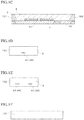
- FIG. 3A is a schematic side view of a light emitting device according to the present disclosure, as seen from a third external lateral surface side.
- FIG. 3B is a schematic side view of a light emitting device according to the present disclosure, as seen from a fourth external lateral surface side.
- FIG. 4A is a schematic side view of a light emitting device according to the present disclosure, as seen from a third external lateral surface side.
- FIG. 4B is a schematic side view of a light emitting device according to the present disclosure, as seen from a fourth external lateral surface side.
- FIG. 4C is a schematic bottom view of a light emitting device according to the present disclosure.
- FIG. 5A is a schematic side view of a light emitting device according to the present disclosure, as seen from a third external lateral surface side.
- FIG. 5B is a schematic side view of a light emitting device according to the present disclosure, as seen from a fourth external lateral surface side.
- FIG. 6A is a schematic top view of a lead frame with resin according to the present disclosure, as seen from an upper surface side.
- FIG. 6B is a schematic top view showing four package portions according to the present disclosure.
- FIG. 6C is a schematic top view showing a lead frame according to the present disclosure.
- FIG. 7 is a schematic top view showing a modified example of a lead frame according to the present disclosure.
- FIG. 8A is a schematic top view of a light emitting device according to a second embodiment according to the present disclosure, as seen from an upper surface side.
- FIG. 8B is a schematic top view showing a shape of a lead of a light emitting device according to the second embodiment according to the present disclosure.
- FIG. 9A is a schematic top view of a light emitting device according to a third embodiment according to the present disclosure, as seen from an upper surface side.
- FIG. 9B is a schematic top view showing a shape of a lead of a light emitting device according to the third embodiment according to the present disclosure.
- a light emitting device and a lead frame with resin according to certain embodiments of the present disclosure will be described in detail below with reference to the drawings.
- the light emitting device and the lead frame with resin described below are intended as illustrative and the present disclosure is not limited to those embodiments described below.
- terms which indicate specific directions or locations for example, “up”, “down” and other terms expressing those) may be applied.
- Those terms are used to express relative directional relationship and positional relationship between the components in a drawing which is referred to for the ease of understanding.
- the sizes and the arrangement relationship of the components in each of drawings are occasionally shown exaggerated for ease of understanding, and may not represent actual dimensions in the light emitting device and/or relationships between the sizes of the components in the actual light emitting device.
- a “long-side direction” indicates a lateral direction (X-direction), which includes the right-direction (X-plus direction) and the left-direction (X-minus direction)
- a “short-side direction” indicates a longitudinal direction (Y-direction), which includes the upward-direction (Y-plus direction) and the downward direction (Y-minus direction), respectively in a drawing which is referred to.
- the terms “package portion” and “lead frame with resin” may be appropriately used both before and after disposing a light emitting element and/or a wire, and/or other components. Also, same terms such as “resin part” may be appropriately used both before and after singulating.
- FIG. 1A is a schematic top view, seen from an upper surface side of a light emitting device 100
- FIG. 1B is a schematic bottom view, seen from a bottom surface side of the light emitting device 100
- FIG. 1C is a schematic end surface view taken along line 1 C- 1 C of FIG. 1A
- FIG. 1D is a schematic side view, seen from a first external lateral surface 101 —side of the light emitting device 100
- FIG. 1E is a schematic side view, seen from a second external lateral surface 102 —side of the light emitting device 100
- FIG. 1D is a schematic side view, seen from a first external lateral surface 101 —side of the light emitting device 100
- FIG. 1E is a schematic side view, seen from a second external lateral surface 102 —side of the light emitting device 100
- FIG. 1D is a schematic side view, seen from a first external lateral surface 101 —side of the light emitting device 100
- FIG. 1E is a
- FIG. 1F is a schematic side view, seen from a third external lateral surface 103 —side of the light emitting device 100
- FIG. 1G is a schematic side view, seen from a fourth external lateral surface 104 —side of the light emitting device 100 .
- the light emitting device 100 includes a resin package 10 having a lead 4 and a resin part 3 , and one or more light emitting elements 1 disposed on the lead 4 .
- the resin package 10 has a rectangular shape when in a top view and has two short-side lateral surfaces and two long-side lateral surfaces.
- the lead 4 is not exposed at the long-side lateral surfaces of the resin package 10 .
- the components of the light emitting device body 100 will be described in detail below.
- the resin package 10 serves as a mounting member of the light emitting elements 1 .
- the resin package 10 includes a lead 4 that includes a first lead 41 and a second lead 42 , and a resin part 3 that holds the lead 4 .
- the resin package 10 shown in FIG. 1A has a recess 2 in the upper surface. Portions of the lead 4 are located at the bottom surface of the recess 2 and the light emitting elements 1 are placed on the first lead 41 of the lead 4 .
- the resin package 10 has a rectangular shape in a top view and having two short-side lateral surfaces and two long-side lateral surfaces.
- the short-side lateral surfaces include a first external lateral surface 101 and a second external lateral surface 102 located opposite side from the first external lateral surface 101 .
- the long-side lateral surfaces include a third external lateral surface 103 and a fourth external lateral surface 104 located opposite side from the third external lateral surface 103 .
- the resin package 10 has an upper surface 10 a and a lower surface 10 b located opposite side from the upper surface 10 a . At the lower surface 10 b of the resin package 10 , a lower surface of the first lead 41 and a lower surface of the second lead 42 are exposed from the resin part 3 .
- the resin package 10 has long-side lateral surfaces and short-side lateral surfaces in which, for example, one or more lateral surfaces among the long-side lateral surfaces and the short-side lateral surfaces may be inclined.
- the resin package 10 may have an anode mark or a cathode mark that is formed by rounding a corner of the opening of the recess.
- the anode mark or the cathode mark serves as a mark indicating a polarity of the lead 4 .
- the lead 4 including the first lead 41 and the second lead 42 has electrically conducting property and serves as electrodes to supply electricity to the light emitting elements 1 .
- the lead 4 may include a third lead 43 in addition to the first lead 41 and the second lead 42 .
- the third lead 43 may serve as a heat dissipating member, or may serve as an electrode like the first lead 41 and the second lead 42 .
- FIG. 2A is a schematic top view showing a shape of the lead 4 of the light emitting device 100
- FIG. 1B is a schematic bottom view showing a shape of the lead 4
- the first lead 41 shown in FIG. 2A has an approximately rectangular main portion 41 a and an approximately rectangular narrow portion 41 b extending from the main portion 41 a in the long-side direction.
- the width of the narrow portion 41 b is smaller than the short-direction width of the main portion 41 a
- the second lead 42 has an approximately rectangular main portion 42 a in a top view, and placed facing a portion of the main portion 41 a and a portion of the narrow portion 41 b of the first lead 41 .
- the first lead 41 has a first lateral side 411 , a second lateral side 412 , a third lateral side 413 , a fourth lateral side 414 , a fifth lateral side 415 , and a sixth lateral side 416 .
- the second lead 42 has a first lateral side 421 , a second lateral side 422 , a third lateral side 423 , and a fourth lateral side 424 .
- the first lateral side 411 of the first lead 41 and the first lateral side 421 of the second lead 42 are located facing the third external lateral surface 103 of the resin package 10 .
- the fourth lateral side 414 of the first lead 41 and the fourth lateral side 424 of the second lead 42 are located facing the second external lateral surface 102 of the resin package 10 .
- the fifth lateral side 415 of the first lead 41 is located facing the fourth external lateral surface 104 of the resin package 10 .
- the sixth lateral side 416 of the first lead 41 is located facing the first external lateral surface 101 of the resin package 10 .
- the first lead 41 is extended from the first external lateral surface 101 of the resin package 10 along the long-side direction to reach the second external lateral surface 102 of the resin package 10 , or is extended from the second external lateral surface 102 of the resin package 10 along the long-side direction to reach the first external lateral surface 101 of the resin package 10 .
- the first lead 41 is extended in the entire long-side direction of the resin package 10 , thus, when a bending stress is experienced in the height direction, the amount of warpage at the long-side lateral surface can be reduced. Accordingly, the strength of the resin package 10 can be improved.
- the first lateral side 411 of the first lead 41 and the first lateral side 421 of the second lead 42 are located in a same plane, or the first lateral side 421 of the second lead 42 is located inward of the first lateral side 411 of the first lead 41 . It is also preferable that, in a top view, the fourth lateral side 414 of the first lead 41 and the fourth lateral side 424 of the second lead 42 are located in a same plane, or the fourth lateral side 424 of the second lead 42 is located inward of the fourth lateral side 414 of the first lead 41 .
- the largest widths of the first lead 41 in the long-side direction and the short-side direction are also the largest widths of the lead 4 in the long-side direction and the short-side direction, respectively.
- reduction in the size of the light emitting device becomes possible.
- the second lateral side 422 of the second lead 42 is spaced apart from the second lateral side 412 of the first lead 41 via a spacing region P.
- the third lateral side 423 of the second lead 42 is spaced apart from the third lateral side 413 of the first lead 41 via a spacing region Q.
- Portions of the resin part 3 are located at the spacing region P and the spacing region Q, respectively.
- the resin part made of a resin material has lower strength than the lead made of a metal member. Thus, when a stress is concentrated near the spacing region P and/or the spacing region Q, cracks may occur in the resin part 3 located below the spacing region P and/or the spacing region Q.
- a portion of the lead 4 is arranged on an imaginary extension line of each of the spacing region P and the spacing region Q. Accordingly, for example, even when a bending stress is experienced near the spacing region P and/or the spacing region Q, the portion of the lead 4 on the imaginary extension line of each of the spacing regions can withstand the stress. Accordingly, the strength of the entire resin package 10 can be improved.
- Each of the main portions 41 a , 42 a , and the narrow portion 41 b may have an extended portion 45 that reaches the first external lateral surface 101 or the second external lateral surface 102 .
- the extended portions 45 are the portions narrower than the corresponding portions of the main portions 41 a , 42 a , and the narrow portion 41 b , respectively.
- the extended portions 45 are provided near the center of the fourth lateral side 414 and the sixth lateral side 416 of the first lead 41 and the fourth lateral side 424 of the second lead 42 , respectively.
- the extended portions 45 are portions of the first lead 41 and the second lead 42 respectively.
- the narrow extended portions 45 increase the respective contact areas of the first lead 41 and the second lead 42 with the resin part 3 and thus tight contact between the lead 4 and the resin part 3 can be increased. Further, when the first external lateral surface 101 and the second external lateral surface 102 is formed by cutting in the lead frame with resin 5 , cutting can be performed at the narrow extended portions 45 and thus stress exerted by cutting can be reduced.
- the lead 4 may have a recessed trough 7 in its upper surface.
- recessed troughs 7 are formed in the upper surfaces of the main portion 41 a and the narrow portion 41 b of the first lead 41 and in the upper surface of the main portion 41 a of the second lead 42 .
- a portion of the resin part 3 is placed in each of the recessed troughs 7 .
- bonding strength between the resin part 3 and the lead 4 can be improved.
- a single recessed trough 7 may be formed in a single lead, or as shown in FIG. 2A , two or more recessed troughs 7 separated by a flat region may be formed in a single lead.
- a lower surface side of each of the first lead 41 and the second lead 42 may be provided with a peripheral depression 8 (indicated by mesh hatching in FIG. 2B ) along the lateral surfaces.
- the peripheral depressions 8 are recessed from the lower surface side toward the upper surface side.
- the peripheral depressions 8 are formed along the first lateral side 411 , the fourth lateral side 414 , the fifth lateral side 415 , and the sixth lateral side 416 of the first lead 41 and along the first lateral side 421 and the fourth lateral side 424 of the second lead 42 , respectively.
- the first lead 41 may be provided with a peripheral depression 8 between the lower surface of the main portion 41 a and the lower surface of the narrow portion 41 b .
- the peripheral depression 8 that separates the lower surface of the main portion 41 a and the lower surface of the narrow portion 41 b , bonding of the resin part 3 and the lead 4 can be improved.
- uneven distribution of the bonding member that is wet-spreading on the surface may result when the lead 41 has an asymmetrical external shape as shown in FIG. 2B .
- the peripheral depression 8 is formed between the lower surface of the main portion 41 a and the lower surface of the narrow portion 41 b , which allows for forming a symmetrical shape such as a rectangular shape of the first lead 41 exposed at the lower surface of the resin package 10 . Accordingly, uneven distribution of the bonding member that is wet-spreading on the surface of the first lead 41 can be reduced.
- the peripheral depression 8 can be formed by etching or pressing.
- the extending portion 45 of the first lead 41 on the first external lateral surface 101 is preferably located on an imaginary straight line passing the center of the light emitting device 100 and extending in the long-side direction.
- the extending portion 45 is exposed on the first external lateral surface 101 or the second external lateral surface 102 , and also approximately flush with the resin part 3 on the first external lateral surface 101 or the second external lateral surface 102 .
- This configuration is obtained by cutting the lead frame with resin 5 at locations corresponding to the short-side lateral surface side (the first external lateral surface 101 and the second external lateral surface 102 ) of the regions to produce each resin package 10 .
- the lower surface of the first lead 41 on the first external lateral surface 101 , the lower surface of the first lead 41 on the second external lateral surface 102 , and the lower surface of the second lead 42 on the second external lateral surface 102 are preferably located spaced apart from the lower surface of the resin package 10 .
- FIG. 3A and FIG. 3B are schematic side views illustrating another example of a light emitting device 100 according to the present disclosure.
- the first lead 41 includes a first upward-opening recess 11 a .
- the first lead 41 includes a second upward-opening recess 11 b and the second lead 42 includes a third upward-opening recess 11 c .
- a portion of the resin part 3 is placed in each of the first upward-opening recess 11 a , the second upward-opening recess 11 b , and the third upward-opening recess 11 c .
- the first upward-opening recess 11 a opens at the first external lateral surface 101 and recessed from the upper surface 10 a side toward the lower surface 10 b side of the resin package 10 .
- the second upward-opening recess 11 b and the third upward-opening recess 11 c respectively open at the second external lateral surface 102 and recessed from the upper surface 10 a side toward the lower surface 10 b side of the resin package 10 .
- the upper surface of the first lead 41 or/and the second lead 42 respectively located on the first external lateral surface 101 and the second external lateral surface 102 are respectively provided with an upward-opening recess and a portion of the resin part 3 is arranged in the upward-opening recess. Accordingly, bonding between the resin part 3 and the lead 4 can be improved.
- FIG. 4A and FIG. 4B are schematic side views and FIG. 4C is a schematic bottom view respectively illustrating another example of the light emitting device 100 .
- the first lead 41 and the second lead 42 are shown exaggerated to illustrate the shapes thereof.
- the lower surface of the first lead 41 on the first external lateral surface 101 and the lower surface of the first lead 41 and the lower surface of the second lead 42 on the second external lateral surface 102 are flush with the lower surface of the resin package 10 . Accordingly, the exposing areas of the first lead 41 and the second lead 42 on the lower surface of the light emitting device 100 can be increased. Accordingly, at the time of bonding the light emitting device 100 on a mounting substrate via a bonding member, the bonding strength between the light emitting device 100 and the mounting substrate can be enhanced.
- the first lead 41 may include a first downward-opening recess 12 a .
- the first lead 41 may include a second downward-opening recess 12 b and the second lead 42 may include a third downward-opening recess 12 c .
- the first downward-opening recess 12 a opens at the lower surface of the resin package 10 and the first external lateral surface 101 , and each of the downward-opening recesses 12 a are recessed from the lower surface toward opposite surface of the lower surface of the resin package 10 .
- the second downward-opening recess 12 b opens both at the lower surface and the second external lateral surface 102 of the resin package 10 and is recessed from the lower surface toward opposite surface of the lower surface of the resin package 10 .
- FIG. 5A and FIG. 5B are schematic side views illustrating a further another example of the light emitting device 100 .
- the lower surface of the first lead 41 or the lower surface of the second lead 42 at the second external lateral surface 102 is located spaced apart from the lower surface of the resin package 10 and the other is located flush with the lower surface of the resin package 10 .
- the lead 4 is not exposed at the third external lateral surface 103 and the fourth external lateral surface 104 that are long-side lateral surfaces.
- the resin part 3 is present at the third external lateral surface 103 and the fourth external lateral surface 104 that are long-side lateral surfaces.
- the lead 4 is not exposed at the long-side lateral surfaces that may be easily bent by bending stress, and thus occurrence of cracks in the resin part 3 that are originated from the lead 4 can be reduced.
- Each of the lead 4 includes a base member and a metal layer that covers the base member.
- the base member preferably has a plate-like shape.
- the base member may include a metal such as copper, aluminum, gold, silver, iron, nickel, or an alloy thereof, phosphor bronze, and iron copper.
- the base member may be made of a single layer or has a layered structure (for example, a cladding material). In particular, copper that is inexpensive and has high heat dissipation performance is preferably used for the base member.
- the metal layer may include, for example, silver, aluminum, nickel, palladium, rhodium, gold, silver, or an alloy thereof.
- the lead 4 may have a region absent of the metal layer.
- the metal layer disposed on the upper surface of the lead 4 and the metal layer disposed on the lower surface of the lead 4 may be different.
- the metal layer disposed on the upper surface of the lead 4 may be a metal layer made of a plurality of layers including a metal layer of nickel
- the metal layer disposed on the lower surface pf the lead 4 may be a metal layer that does not contain a nickel layer.
- a protective layer of such as silicon oxide is preferably provided on the plated layer containing silver. With this arrangement, discoloration of the plated layer containing silver caused by sulfur in the air can be reduced.
- the protective layer can be disposed using a vacuum process such as sputtering, or using another known method.
- a thermosetting resin, a thermoplastic resin, or the like can be used as a base resin material.
- a base resin material includes a cured product of an epoxy resin composition, a silicone resin composition, a modified epoxy resin composition such as a silicone-modified epoxy resin, an unsaturated polyester resin, a saturated polyester resin, a polyimide resin composition, a modified polyimide resin composition, a polyphthalamide (PPA), a polycarbonate resin, a polyphenylene sulfide (PPS), a liquid polymer (LCP), an ABS resin, a phenol resin, an acrylic resin, and a PBT resin.
- a thermosetting resin such as an epoxy resin composition or a modified silicone resin composition is preferably used.
- examples of preferable resin material for the resin part 3 include a silicone resin compound (for example a SMC resin) having good heat-resisting and light-resisting properties.
- the resin part 3 may have a low reflectance to external light (in many cases, sun light) to improve the contrast of the light emitting device.
- a black color or a color close to black is preferable.
- an appropriate filler material can be used according to intended usage. Examples thereof include carbon such as acetylene black, activated carbon, and graphite, a transmission metal oxide such as iron oxide, manganese dioxide, cobalt oxide, and molybdenum oxide, and a chromatic organic pigment.
- One or more light emitting elements 1 are disposed on the upper surface of the lead 4 .
- a light emitting diode element or the like can be employed.
- the light emitting element 1 particularly preferably include a nitride-based semiconductor (In x Al y Ga 1-x-y N, 0 ⁇ x, 0 ⁇ y, x+y ⁇ 1) that can emit light in a range of ultraviolet to visible light.
- the light emitting device has two light emitting elements, but a single light emitting element or three or more light emitting elements can be employed.
- a light emitting element to emit blue light and a light emitting element to emit green light may be employed.
- the light emitting device has three light emitting elements, a light emitting element to emit blue light, a light emitting element to emit green light, and a light emitting element to emit red light may be employed.
- a sealing member may be disposed in the recess 2 .
- the sealing member covers the light emitting element 1 placed at the bottom of the recess 2 , so that the light emitting element 1 can be protected from external force, dusts, moisture, or the like.
- the sealing member can transmit 60% or greater, more preferably 90% or greater light emitted from the light emitting element 1 .
- a resin material used for the resin part 3 can also be used.
- a thermosetting resin, a thermoplastic resin, or the like can be used, and for example, a silicone resin, an epoxy resin, an acrylic resin, or a resin containing one or more of those can be used.
- the sealing member may be formed with a single layer or a plurality of layers. Further, light scattering particles of titanium oxide, silicon oxide, zirconium oxide, or/and aluminum oxide may be dispersed in the sealing member.
- the sealing member may contain a material (such as a fluorescent material) that can convert the wavelength of light emitted from the light emitting element 1 .
- a material such as a fluorescent material
- the fluorescent material include yttrium aluminum garnet activated with cerium, lutetium aluminum garnet activated with cerium, nitrogen-containing calcium aluminosilicate (portion of calcium can be substituted with strontium) activated with europium and/or chromium, sialon activated with europium, silicate activated with europium, strontium aluminate activated with europium, and potassium fluosilicate activated with manganese.
- the light scattering particles and/or the fluorescent material is preferably contained in a range of about 10 to about 100 weight % with respect to the total weight of the sealing member.
- the light emitting device 100 may further include a protective element such as Zener diode.
- the protective element is mounted on the upper surface of the lead 4 at the bottom surface of the recess 2 .
- the first lead 41 has the main portion 41 a and the narrow portion 41 b
- the light emitting element 1 is disposed on the main portion 41 a and the protective element is disposed on the narrow portion 41 b .
- the lead 4 is not exposed at the long-side lateral surface side that may be easily bent by bending stress, so that occurrence of cracks in the resin part 3 that are originated from the lead 4 can be reduced.
- FIG. 6A is a schematic top view of a lead frame with resin 5 seen from above
- FIG. 6B is a schematic top view showing four package portions 50
- FIG. 6C is a schematic top view showing a lead frame 6 .
- the lead frame with resin 5 includes a lead frame 6 and a resin part 3 formed in an integral manner with the lead frame 6 .
- the lead frame with resin 5 defines a plurality of recesses 2 in its upper side.
- first lead portion 61 On the bottom surface of each of the recesses 2 , a portion of the lead frame to be singulated to provide a first lead 41 (hereinafter to be referred to as “first lead portion 61 ”) and a portion of the lead frame to be singluraled to provide a second lead 42 (hereinafter to be referred to as “second lead portion 62 ”) are both located.
- the light emitting element(s) 1 and the sealing member are to be disposed in the recess 2 .
- the lead frame with resin 5 includes a plurality of package portions 50 .
- FIG. 6B four package portions 50 are illustrated.
- Each of the package portions 50 is indicated by the region surrounded by the predetermined cutting lines (dotted lines) extending in the row direction and in the column direction in FIG. 6B .
- Each of the package portions 50 has a rectangular shape having long-sides and short-sides in a top view, and includes the first lead portion 61 , the second lead portion 62 , and a portion of the resin part 3 .
- the resin part 3 is integrally formed connecting a single package portion 50 with its adjacent package portions 50 .
- FIG. 6B four package portions 50 are illustrated.
- Each of the package portions 50 is indicated by the region surrounded by the predetermined cutting lines (dotted lines) extending in the row direction and in the column direction in FIG. 6B .
- Each of the package portions 50 has a rectangular shape having long-sides and short-sides in a top view, and includes the first lead portion 61 , the second lead
- the resin part 3 constituting an upper surface of a single package portion 50 , the resin parts 3 constituting respective upper surfaces of other package portions 50 , and the resin part 3 located in the vicinity of the predetermined cutting lines between two adjacent package portions 50 are flush with each other.
- the lead frame 6 used in the lead frame with resin 5 is illustrated.
- the lead frame 6 includes a plurality of lead portions 60 and a plurality of supporting parts 64 .
- Each of the lead portions 60 is a portion to be singulated to provide the lead 4 .
- the plurality of lead portions 60 are arranged in columns and rows in the lead frame 6 .
- Each of the lead portion 60 includes the first lead portion 61 and the second lead portion 62 arranged in the row direction.
- Each of the first lead portions 61 reaches both the short sides of the package portion 50 .
- the first lead portion 61 is connected to the supporting part 64 at one of the two short-sides of the package portion 50 .
- the first lead portion 61 and the second lead portion 62 are connected to the supporting part 64 at the other of the two short-sides of the package portion 50 . Meanwhile, the lead portion 60 and the supporting part 64 are not connected at the two long-sides of the package portion 50 .
- the lead frame 6 is cut along the supporting part 64 .
- the predetermined cutting lines are indicated by shading.
- the supporting part 64 can be removed in singulating by, for example, using a blade of a dicing saw or the like, having a width greater than the width of the supporting part 64 , such that the supporting part 64 does not remain in the singulated light emitting device 100 .
- the lead frame 6 and the resin part 3 are cut together in singulating the lead frame with resin 5 according to the present disclosure. More specifically, at the two short-sides of the package portion 50 , the resin part 3 , the supporting part 64 , and a portion of the lead portion 60 are cut together. At the two long-sides of the package portion 50 , the resin part 3 and the supporting part 64 are cut together. By such cutting, the resin part 3 and a portion of lead 4 exposed from the resin part 3 are located on the short-side lateral surfaces of the singulated resin package. Meanwhile, only the resin part 3 is present at the long-side lateral surfaces of the resin package 10 .
- Singulating the lead frame with resin 5 can be selected from various methods such as cutting with a lead-cutting mold, cutting with a dicing saw, and cutting with a laser light.
- the lead portion 60 is not present at the two long-side lateral surfaces of the package portion.
- occurrence of cracks originated from the lead portion 60 can be reduced.
- absence of the lead portion 60 at the long-side lateral surfaces that create a large cutting area can reduce the total stress exerted on the lead portion 60 .
- problems such as deformation of the lead portion 60 can be reduced.
- FIG. 7 is a schematic top view showing a modified example of the lead frame 6 .
- the lead frame 6 shown in FIG. 7 differs from the lead frame shown in FIG. 6C in that a single lead portion 60 and adjacent lead portions are directly connected to each other in FIG. 7 without being connected through the supporting part 64 . More specifically, the lead frame 6 shown in FIG. 7 has a first lead unit 60 a , a second lead unit 60 b , and a third lead unit 60 c connected in this order in a row direction.
- the first lead portion 61 of the second lead unit 60 b is directly connected to the first lead portion 61 and the second lead portion 62 of the first lead unit 60 a without being connected through other portions of the lead frame 6 .
- the first lead portion 61 and the second lead portion 62 of the second lead unit 60 b are directly connected to the first lead portion 61 of the third lead unit 60 c without being connected through other portions of the lead frame 6 .
- FIG. 8A is a schematic top view of a light emitting device 200 seen from above
- FIG. 8B is a schematic top view of a lead 4 of the light emitting device 200 .
- the light emitting device 200 according to the second embodiment has a configuration similar to that of the light emitting device 100 according to the first embodiment, except that in the light emitting device 200 , the second lead 42 is exposed at the first external lateral surface 101 and is also flush with the resin part 3 in the first external lateral surface 101 .
- the light emitting device 200 includes a resin package 10 having a first lead 41 , a second lead 42 , and the resin part 3 , and one or more light emitting elements 1 mounted on the resin package 10 .
- the resin package 10 has a rectangular shape in a top view and having two short-side lateral surfaces and two long-side lateral surfaces.
- the first lead 41 and the second lead 42 are exposed at the first external lateral surface 101 and also are flush with the resin part 3 in the first external lateral surface 101 .
- the first lead 41 and the second lead 42 are exposed at the second external lateral surface 102 , and also are flush with the resin part 3 in the second external lateral surface 102 .
- both ends of the first lead 41 and the second lead 42 are respectively reach the first external lateral surface 101 and the second external lateral surface 102 .
- both ends of the first lead 41 and the second lead reach the first external lateral surface 101 and the second external lateral surface 102 , respectively.
- the first lead 41 and the second lead 42 are not exposed from the resin part 3 .
- the lead 4 is not exposed at the long-side lateral surface side that may be easily bent by bending stress, so that occurrence of cracks in the resin part 3 that are originated from the lead 4 can be reduced.
- FIG. 9A is a schematic top view of a light emitting device 300
- FIG. 9B is a schematic top view showing a shape of a lead 4 of the light emitting device 300 .
- the light emitting device 300 according to the third embodiment has a configuration similar to that of the light emitting device 100 according to the first embodiment, except that a third lead 43 is further provided in the light emitting device 300 .
- the light emitting device 300 includes a resin package 10 having a first lead 41 , a second lead 42 , a third lead 43 , and a resin part 3 , and one or more light emitting elements 1 mounted on the resin package 10 .
- the second lead 42 and the third lead 43 are disposed facing the first lead 41 .
- the second lead 42 and the third lead 43 are disposed facing each other.
- the first lead 41 is disposed facing the spacing region, which allows for an improvement in the mechanical strength of the light emitting device 300 .
- the first lead 41 , the second lead 42 , and the third lead 43 are not exposed from the resin part 3 .
- the lead 4 is not exposed at the long-side lateral surface side that may be easily bent by bending stress, so that occurrence of cracks in the resin part 3 that are originated from the lead 4 can be reduced.
Landscapes
- Engineering & Computer Science (AREA)
- Microelectronics & Electronic Packaging (AREA)
- Power Engineering (AREA)
- Computer Hardware Design (AREA)
- Manufacturing & Machinery (AREA)
- Physics & Mathematics (AREA)
- Condensed Matter Physics & Semiconductors (AREA)
- General Physics & Mathematics (AREA)
- Ceramic Engineering (AREA)
- Led Device Packages (AREA)
Abstract
Description
Claims (18)
Applications Claiming Priority (2)
| Application Number | Priority Date | Filing Date | Title |
|---|---|---|---|
| JP2017-125684 | 2017-06-27 | ||
| JP2017125684A JP6680274B2 (en) | 2017-06-27 | 2017-06-27 | Light emitting device and lead frame with resin |
Publications (2)
| Publication Number | Publication Date |
|---|---|
| US20180375004A1 US20180375004A1 (en) | 2018-12-27 |
| US10847693B2 true US10847693B2 (en) | 2020-11-24 |
Family
ID=64692811
Family Applications (1)
| Application Number | Title | Priority Date | Filing Date |
|---|---|---|---|
| US16/019,408 Active 2038-07-03 US10847693B2 (en) | 2017-06-27 | 2018-06-26 | Light emitting device and lead frame with resin |
Country Status (2)
| Country | Link |
|---|---|
| US (1) | US10847693B2 (en) |
| JP (1) | JP6680274B2 (en) |
Citations (16)
| Publication number | Priority date | Publication date | Assignee | Title |
|---|---|---|---|---|
| JPS63159859U (en) | 1987-04-07 | 1988-10-19 | ||
| JP2007288198A (en) | 2006-04-17 | 2007-11-01 | Samsung Electro-Mechanics Co Ltd | Light emitting diode package and its manufacturing method |
| US7982709B2 (en) * | 2005-11-11 | 2011-07-19 | Hitachi Displays, Ltd. | Illuminating device and liquid-crystal display device using the same |
| US20120080674A1 (en) * | 2010-01-29 | 2012-04-05 | Kabushiki Kaisha Toshiba | Led package |
| US20120127720A1 (en) * | 2010-06-28 | 2012-05-24 | Hussell Christopher P | Light emitting devices and methods |
| JP2012182180A (en) | 2011-02-28 | 2012-09-20 | Toppan Printing Co Ltd | Lead frame substrate for led element and light emitting element |
| US20120273826A1 (en) | 2011-04-28 | 2012-11-01 | Kabushiki Kaisha Toshiba | Led package and method for manufacturing same |
| US20120300491A1 (en) * | 2011-01-31 | 2012-11-29 | Hussell Christopher P | High brightness light emitting diode (led) packages, systems and methods with improved resin filling and high adhesion |
| US20130070452A1 (en) * | 2010-04-26 | 2013-03-21 | Panasonic Corporation | Lead frame, wiring board, light emitting unit, and illuminating apparatus |
| US20130214298A1 (en) * | 2011-07-21 | 2013-08-22 | Cree Inc. | Light emitter device packages, components, and methods for improved chemical resistance and related methods |
| JP2014022491A (en) | 2012-07-17 | 2014-02-03 | Citizen Holdings Co Ltd | Semiconductor light-emitting device and manufacturing method of the same |
| US20140043855A1 (en) * | 2012-08-08 | 2014-02-13 | Samsung Display Co., Ltd. | Backlight assembly and display apparatus having the same |
| US20140183574A1 (en) * | 2012-12-29 | 2014-07-03 | Nichia Corporation | Light emitting device package, light emitting device using that package, and illumination device using the light emitting devices |
| US20150129899A1 (en) * | 2013-11-08 | 2015-05-14 | Osram Sylvania Inc. | Led lead frame for laminated led circuits |
| US20160027720A1 (en) * | 2007-10-16 | 2016-01-28 | Kabushiki Kaisha Toshiba | Semiconductor device and lead frame used for the same |
| JP2016021561A (en) | 2014-06-17 | 2016-02-04 | 大日本印刷株式会社 | Lead frame with resin, multifaceted body having lead frame with resin, optical semiconductor device and multifaceted body of optical semiconductor device |
Family Cites Families (9)
| Publication number | Priority date | Publication date | Assignee | Title |
|---|---|---|---|---|
| DE29825062U1 (en) * | 1997-07-29 | 2004-07-22 | Osram Opto Semiconductors Gmbh | Optoelectronic component |
| US7183588B2 (en) * | 2004-01-08 | 2007-02-27 | Avago Technologies Ecbu Ip (Singapore) Pte. Ltd. | Light emission device |
| JP5026848B2 (en) * | 2007-04-19 | 2012-09-19 | スタンレー電気株式会社 | Optical semiconductor device and manufacturing method thereof |
| JP2011071265A (en) * | 2009-09-25 | 2011-04-07 | Toshiba Corp | Light-emitting apparatus |
| JP5010716B2 (en) * | 2010-01-29 | 2012-08-29 | 株式会社東芝 | LED package |
| JP2012124249A (en) * | 2010-12-07 | 2012-06-28 | Toshiba Corp | Led package and manufacturing method thereof |
| JP5693313B2 (en) * | 2011-03-23 | 2015-04-01 | シチズン電子株式会社 | Manufacturing method of semiconductor light emitting device using lead frame |
| JP6268793B2 (en) * | 2013-08-02 | 2018-01-31 | 大日本印刷株式会社 | Multi-sided body of lead frame, multi-sided body of lead frame with resin, multi-sided body of optical semiconductor device, lead frame, lead frame with resin, optical semiconductor device |
| WO2017080605A1 (en) * | 2015-11-12 | 2017-05-18 | Osram Opto Semiconductors Gmbh | Package for an electronic component, electronic component and electronic arrangement |
-
2017
- 2017-06-27 JP JP2017125684A patent/JP6680274B2/en active Active
-
2018
- 2018-06-26 US US16/019,408 patent/US10847693B2/en active Active
Patent Citations (18)
| Publication number | Priority date | Publication date | Assignee | Title |
|---|---|---|---|---|
| JPS63159859U (en) | 1987-04-07 | 1988-10-19 | ||
| US7982709B2 (en) * | 2005-11-11 | 2011-07-19 | Hitachi Displays, Ltd. | Illuminating device and liquid-crystal display device using the same |
| JP2007288198A (en) | 2006-04-17 | 2007-11-01 | Samsung Electro-Mechanics Co Ltd | Light emitting diode package and its manufacturing method |
| US20160027720A1 (en) * | 2007-10-16 | 2016-01-28 | Kabushiki Kaisha Toshiba | Semiconductor device and lead frame used for the same |
| US20120080674A1 (en) * | 2010-01-29 | 2012-04-05 | Kabushiki Kaisha Toshiba | Led package |
| US20130070452A1 (en) * | 2010-04-26 | 2013-03-21 | Panasonic Corporation | Lead frame, wiring board, light emitting unit, and illuminating apparatus |
| US20120127720A1 (en) * | 2010-06-28 | 2012-05-24 | Hussell Christopher P | Light emitting devices and methods |
| US20120300491A1 (en) * | 2011-01-31 | 2012-11-29 | Hussell Christopher P | High brightness light emitting diode (led) packages, systems and methods with improved resin filling and high adhesion |
| JP2012182180A (en) | 2011-02-28 | 2012-09-20 | Toppan Printing Co Ltd | Lead frame substrate for led element and light emitting element |
| JP2012234955A (en) | 2011-04-28 | 2012-11-29 | Toshiba Corp | Led package and method for manufacturing the same |
| US20120273826A1 (en) | 2011-04-28 | 2012-11-01 | Kabushiki Kaisha Toshiba | Led package and method for manufacturing same |
| US20130214298A1 (en) * | 2011-07-21 | 2013-08-22 | Cree Inc. | Light emitter device packages, components, and methods for improved chemical resistance and related methods |
| JP2014022491A (en) | 2012-07-17 | 2014-02-03 | Citizen Holdings Co Ltd | Semiconductor light-emitting device and manufacturing method of the same |
| JP5930893B2 (en) | 2012-07-17 | 2016-06-08 | シチズンホールディングス株式会社 | Manufacturing method of semiconductor light emitting device |
| US20140043855A1 (en) * | 2012-08-08 | 2014-02-13 | Samsung Display Co., Ltd. | Backlight assembly and display apparatus having the same |
| US20140183574A1 (en) * | 2012-12-29 | 2014-07-03 | Nichia Corporation | Light emitting device package, light emitting device using that package, and illumination device using the light emitting devices |
| US20150129899A1 (en) * | 2013-11-08 | 2015-05-14 | Osram Sylvania Inc. | Led lead frame for laminated led circuits |
| JP2016021561A (en) | 2014-06-17 | 2016-02-04 | 大日本印刷株式会社 | Lead frame with resin, multifaceted body having lead frame with resin, optical semiconductor device and multifaceted body of optical semiconductor device |
Also Published As
| Publication number | Publication date |
|---|---|
| JP6680274B2 (en) | 2020-04-15 |
| US20180375004A1 (en) | 2018-12-27 |
| JP2019009363A (en) | 2019-01-17 |
Similar Documents
| Publication | Publication Date | Title |
|---|---|---|
| US8753907B2 (en) | Semiconductor light emitting device and method for manufacturing the same | |
| US9793249B2 (en) | Light emitting device and light unit having the same | |
| US9281460B2 (en) | Light emitting device package and light emitting device having lead-frames | |
| US10340433B2 (en) | Light emitting device | |
| US10629790B2 (en) | Light-emitting device | |
| US20120161180A1 (en) | Led package | |
| US20170213944A1 (en) | Light emitting device | |
| US10622528B2 (en) | Light-emitting device | |
| JP7046796B2 (en) | Light emitting device | |
| US9991237B2 (en) | Light emitting device | |
| JP2012049348A (en) | Light emitting device | |
| JP2014225644A (en) | Light-emitting device | |
| US10332824B2 (en) | Lead frame | |
| US9698328B2 (en) | Light emitting device | |
| US9502618B2 (en) | LED module | |
| US10193028B2 (en) | Light emitting device and method of producing the same | |
| US10847693B2 (en) | Light emitting device and lead frame with resin | |
| US11257994B2 (en) | Resin package and light emitting device | |
| US20220320388A1 (en) | Light emitting device | |
| JP7208490B2 (en) | Resin package and light emitting device | |
| US9997503B2 (en) | Composite substrate and light emitting device | |
| JP2016119464A (en) | Light emitting device | |
| JP6735545B2 (en) | Light emitting device | |
| JP2019216265A (en) | Manufacturing method of light-emitting device |
Legal Events
| Date | Code | Title | Description |
|---|---|---|---|
| AS | Assignment |
Owner name: NICHIA CORPORATION, JAPAN Free format text: ASSIGNMENT OF ASSIGNORS INTEREST;ASSIGNORS:YAMASHITA, RYOHEI;AKAGAWA, SEITARO;HASHIMOTO, TOSHIYUKI;AND OTHERS;SIGNING DATES FROM 20180614 TO 20180615;REEL/FRAME:046208/0678 |
|
| FEPP | Fee payment procedure |
Free format text: ENTITY STATUS SET TO UNDISCOUNTED (ORIGINAL EVENT CODE: BIG.); ENTITY STATUS OF PATENT OWNER: LARGE ENTITY |
|
| STPP | Information on status: patent application and granting procedure in general |
Free format text: DOCKETED NEW CASE - READY FOR EXAMINATION |
|
| STPP | Information on status: patent application and granting procedure in general |
Free format text: NON FINAL ACTION MAILED |
|
| STPP | Information on status: patent application and granting procedure in general |
Free format text: NON FINAL ACTION MAILED |
|
| STPP | Information on status: patent application and granting procedure in general |
Free format text: RESPONSE TO NON-FINAL OFFICE ACTION ENTERED AND FORWARDED TO EXAMINER |
|
| STPP | Information on status: patent application and granting procedure in general |
Free format text: PUBLICATIONS -- ISSUE FEE PAYMENT VERIFIED |
|
| STCF | Information on status: patent grant |
Free format text: PATENTED CASE |
|
| MAFP | Maintenance fee payment |
Free format text: PAYMENT OF MAINTENANCE FEE, 4TH YEAR, LARGE ENTITY (ORIGINAL EVENT CODE: M1551); ENTITY STATUS OF PATENT OWNER: LARGE ENTITY Year of fee payment: 4 |