EP4080249B1 - Auf einer oberfläche eines szintillators angeordnete lichtsensoren - Google Patents
Auf einer oberfläche eines szintillators angeordnete lichtsensoren Download PDFInfo
- Publication number
- EP4080249B1 EP4080249B1 EP22174855.1A EP22174855A EP4080249B1 EP 4080249 B1 EP4080249 B1 EP 4080249B1 EP 22174855 A EP22174855 A EP 22174855A EP 4080249 B1 EP4080249 B1 EP 4080249B1
- Authority
- EP
- European Patent Office
- Prior art keywords
- scintillator
- photosensor
- radiation detector
- discrete
- disposed
- Prior art date
- Legal status (The legal status is an assumption and is not a legal conclusion. Google has not performed a legal analysis and makes no representation as to the accuracy of the status listed.)
- Active
Links
Images




Classifications
-
- G—PHYSICS
- G01—MEASURING; TESTING
- G01T—MEASUREMENT OF NUCLEAR OR X-RADIATION
- G01T1/00—Measuring X-radiation, gamma radiation, corpuscular radiation, or cosmic radiation
- G01T1/16—Measuring radiation intensity
- G01T1/20—Measuring radiation intensity with scintillation detectors
- G01T1/2018—Scintillation-photodiode combinations
- G01T1/20185—Coupling means between the photodiode and the scintillator, e.g. optical couplings using adhesives with wavelength-shifting fibres
-
- G—PHYSICS
- G01—MEASURING; TESTING
- G01T—MEASUREMENT OF NUCLEAR OR X-RADIATION
- G01T1/00—Measuring X-radiation, gamma radiation, corpuscular radiation, or cosmic radiation
- G01T1/16—Measuring radiation intensity
- G01T1/20—Measuring radiation intensity with scintillation detectors
- G01T1/2002—Optical details, e.g. reflecting or diffusing layers
-
- G—PHYSICS
- G01—MEASURING; TESTING
- G01T—MEASUREMENT OF NUCLEAR OR X-RADIATION
- G01T1/00—Measuring X-radiation, gamma radiation, corpuscular radiation, or cosmic radiation
- G01T1/16—Measuring radiation intensity
- G01T1/20—Measuring radiation intensity with scintillation detectors
- G01T1/2018—Scintillation-photodiode combinations
- G01T1/20184—Detector read-out circuitry, e.g. for clearing of traps, compensating for traps or compensating for direct hits
-
- G—PHYSICS
- G01—MEASURING; TESTING
- G01T—MEASUREMENT OF NUCLEAR OR X-RADIATION
- G01T1/00—Measuring X-radiation, gamma radiation, corpuscular radiation, or cosmic radiation
- G01T1/16—Measuring radiation intensity
- G01T1/20—Measuring radiation intensity with scintillation detectors
- G01T1/2018—Scintillation-photodiode combinations
- G01T1/20186—Position of the photodiode with respect to the incoming radiation, e.g. in the front of, below or sideways the scintillator
-
- G—PHYSICS
- G01—MEASURING; TESTING
- G01T—MEASUREMENT OF NUCLEAR OR X-RADIATION
- G01T1/00—Measuring X-radiation, gamma radiation, corpuscular radiation, or cosmic radiation
- G01T1/16—Measuring radiation intensity
- G01T1/20—Measuring radiation intensity with scintillation detectors
- G01T1/2018—Scintillation-photodiode combinations
- G01T1/20187—Position of the scintillator with respect to the photodiode, e.g. photodiode surrounding the crystal, the crystal surrounding the photodiode, shape or size of the scintillator
Definitions
- the present disclosure is directed to the arrangement of photosensors on a scintillator and methods of using such scintillators and photosensors in a radiation detector.
- Scintillator-based detectors are used in a variety of applications, including research in nuclear physics, oil exploration, field spectroscopy, container and baggage scanning, and medical diagnostics.
- a scintillator material of the scintillator-based detector When a scintillator material of the scintillator-based detector is exposed to ionizing radiation, the scintillator material captures energy of incoming radiation and scintillates, emitting the captured energy in the form of photons.
- a photosensor of the scintillator-based detector detects the emitted photons. Radiation detection apparatuses can analyze pulses for many different reasons. Continued improvements are desired.
- the patent publication JP 5150219 B2 discloses a scintillator crystal coupled to a segmented photodiode.
- the term "energy resolution” (also referred to as PHR for pulse height resolution) refers to a parameter measured by recording a spectrum representing the activity of a source as a function of energy, this spectrum describing the full width at half maximum ("FWHM") of a peak which divided by the energy (abscissa of the peak maximum), multiplied by 100%, gives the PHR as a percentage-the lower the PHR, the better the spectral resolution.
- FWHM full width at half maximum
- the terms “comprises,” “comprising,” “includes,” “including,” “has,” “having,” or any other variation thereof, are intended to cover a non-exclusive inclusion.
- a process, method, article, or apparatus that comprises a list of features is not necessarily limited only to those features but may include other features not expressly listed or inherent to such process, method, article, or apparatus.
- “or” refers to an inclusive-or and not to an exclusive-or. For example, a condition A or B is satisfied by any one of the following: A is true (or present) and B is false (or not present), A is false (or not present) and B is true (or present), and both A and B are true (or present).
- a radiation detector 10 can include a scintillator 20 and a photosensor system 30 disposed on a scintillator surface 22.
- the photosensor system 30 is placed only on the scintillator surface 22.
- a photosensor can also be disposed on a side surface 23 of the scintillator 20.
- a total coverage of 15 to 30%, or even 20 to 25% can achieve approximately the same energy resolution as 100% coverage for a NaI(Tl) scintillator.
- the photosensor system 30 does not occupy any area within a distance of the center point of the scintillator surface 22 that is 10% of the distance from the center point of the scintillator surface 22 to the nearest peripheral edge of the scintillator surface 22.
- the cumulative area can represent a total area occupied by the photosensor system or a total active area of the photosensor system.
- a layer of optical coupling material can be disposed on the photosensor 31, the scintillator 20, the optical window 11 if present, or any combination thereof.
- the optical coupling material can include a grease, a resin, an adhesive, or any combination thereof, disposed between the scintillator 20 and the photosensor 31.
- the optical coupling material can also be transmissive to scintillation light given off by the scintillator 20.
- the discrete photosensors 31 can have alternative shapes that generally fit in the area near the corner or along the peripheral edges of scintillator surface 22.
- the discrete photosensors 31 can have a triangular shape such that a corner of the triangular shape is disposed on a corner of scintillator surface 22.
- the shortest distance from the peripheral edge of the discrete photosensor 31 to the nearest peripheral edge of the scintillator surface 22 is at most 3 mm, or at most 2 mm, or at most 1 mm. If not flush, the shortest distance from the peripheral edge of the discrete photosensor 31 to the nearest peripheral edge of the scintillator surface 22 may be at least 1 micron.
- the scintillator surface 22 can have a polygonal shape, an arcuate shape, an irregular shape, or the like.
- the scintillator surface 22 has a polygonal shape having a plurality of corners, such as at least 3 corners, or at least 4 corners.
- the polygonal shape has at most 10 corners, or at most 9 corners, or at most 8 corners.
- the polygonal shape includes a rectangular shape and, in the embodiment illustrated in FIGs. 1 and 2 , the scintillator surface 22 has a square shape.
- the scintillator surface 22 has an oval shape or a circle shape.
- the scintillator surface 22 can have an average width W S calculated by taking an average of the shortest distance from the center point of the scintillator surface 22 to each peripheral edge of the scintillator surface 22.
- the average width W S is calculated by taking an average of the diameter along the major axis and the diameter along the minor axis.
- the scintillator surface 22 has an average width W S of at least 10 mm, or at least 15 mm, or at least 20 mm.
- surface 22 has an average width W S of at most 600 mm, or at most 500 mm, or at most 400 mm.
- surface 22 can have an average width W S in a range of any of the above minimum or maximum values, such as 15 to 600 mm, or 20 to 500, or 20 to 400 mm.
- the photosensor system 30 can be disposed on more than one surface of the scintillator 20. In an embodiment the photosensor system 30 can be disposed on opposing scintillator surfaces, each having discrete photosensors 31 disposed thereon. In the embodiment illustrated in FIG. 2 , the discrete photosensors 31 are only disposed on opposing scintillator surfaces 22 and 24.
- the scintillator surface 24, and a discrete photosensor 31 disposed on the scintillator surface 24, can have one or more of the features described above with respect to the scintillator surface 22, and a discrete photosensor 31 disposed on the scintillator surface 22.
- the size and shape of scintillator surfaces 22 and 24 can be the same or different.
- the shape of the scintillator surfaces 22 and 24 can be the same while the sizes of surfaces 22 and 24 are different, such as a frustum of a cone or pyramid.
- the arrangement of the discrete photosensors 31 on the scintillator surfaces 22 and 24 can be the same or different.
- the scintillator 20 can have a length L measured from the scintillator surface 22 to the scintillator surface 24.
- the length L is greater than or equal to the average width W S of the scintillator surface 22.
- the length L can be at least 10 mm, or at least 20 mm, or at least 30 mm.
- the length L can be at most 5000 mm, or at most 4000 mm, or at most 3000 mm.
- the length L can be in a range of any of the above minimum and maximum values, such as 10 to 5000 mm, or 20 to 4000 mm, or 30 to 3000 mm.
- the scintillator can have a length L within the values discussed above, after reading this specification, a person of ordinary skill in the art will understand how the photosensor system 30 discussed herein could be applied to the surface of a scintillator having a length L that is less than or greater than the values discussed above.
- the scintillator 20 can be a cube having the dimensions of at least 25 mm ⁇ 25 mm ⁇ 25 mm or at least 50 mm ⁇ 50 mm ⁇ 50 mm. In an embodiment, scintillator 20 can be a cuboid having the dimensions of at least 25 mm ⁇ 25 mm ⁇ 50 mm; or at least 50 mm ⁇ 50 mm ⁇ 100 mm; or at least 50 mm ⁇ 100 mm ⁇ 400 mm; or at least 100 mm ⁇ 100 mm ⁇ 400 mm.
- the scintillator 20 can be a cylinder having a diameter of at least 25 mm, or at least 50 mm, or at least 75 mm, or at least 100 mm, or at least 125 mm, and a length of at least 25 mm, or at least 50 mm, or at least 75 mm, or at least 100 mm, or at least 125 mm.
- the length L of the cylinder is the same as the average width W S of the scintillator surface 22 of the cylinder.
- the length L of the cylinder is greater than the diameter of the scintillator surface 22 of the cylinder, even at least twice the diameter of the cylinder.
- the aspect ratio of the scintillator 20 can be within a range of any of the above minimum and maximum values, such as 1.4 to 6.5, or 1.6 to 6, or 1.8 to 5.5.
- scintillator 20 can include a scintillator material that is particularly suited for a particular application, so long as a photosensor 30 can be disposed on scintillator 20.
- the scintillator material is an inorganic scintillator material.
- the inorganic scintillator material can include a sodium iodide, a cesium iodide, a bismuth germinate, a lanthanum bromide, a cerium bromide, a lanthanum chloride, a lutetium oxyorthosilicate, a lutetium yttrium oxyorthosilicate, a cesium lithium lanthanum bromide, a cesium lithium lanthanum bromo-chloride, a cesium lithium yttrium chloride, or any combination thereof.
- the scintillator is an organic scintillator material.
- the organic scintillator material can include a plastic scintillator, an anthracene, a stilbene, or any combination thereof.
- the scintillator 20 can be a monolithic scintillator.
- an advantage of the radiation detector described herein includes achieving improved performance while the photosensor cumulatively occupies less than the full area of the surface of the scintillator.
- the radiation detector 10 can have an improved single-end light collection efficiency and dual-end light collection efficiency.
- single-end at least when used with respect to performance parameters of the radiation detector 10 refers to a measurement taken from a single end surface of the scintillator
- dual-end at least when used with respect to performance parameters of the radiation detector, refers to a measurement taken from a two opposing end surfaces of the scintillator.
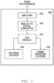
- the radiation detector 10 can further include an analyzer device electrically coupled to the photosensors 30, as illustrated in FIG. 7 .
- the analyzer device 262 can include hardware and can be at least partly implemented in software, firmware, or a combination thereof.
- the hardware can include a plurality of circuits within an field-programmable gate array (FPGA), an application-specific integrated circuit (ASIC), another integrated circuit or on a printed circuit board, or another suitable device, or any combination thereof.
- the analyzer device 262 can also include a buffer to temporarily store data before the data are analyzed, written to storage, read, transmitted to another component or device, another suitable action is performed on the data, or any combination thereof.
- any of the scintillators as previously described can be used in a variety of applications.
- Exemplary applications include radiation detectors for security applications, oil well-logging detectors, gamma ray spectroscopy, isotope identification, Single Positron Emission Computer Tomography (SPECT) or Positron Emission Tomography (PET) analysis, and x-ray imaging.
- the radiation detectors for security applications can include a portal monitor radiation detector, a handheld radiation detector, and a personal radiation detector.
- the simulation was based on cuboidal NaI scintillators having the dimensions of 4 inches (about 10.2 cm) ⁇ 4 inches (about 10.2 cm) ⁇ 16 inches (about 40.6 cm) and plurality of discrete photosensors placed on one or opposing surfaces of the cuboidal NaI scintillators in a corner configuration (see FIG. 4 ), an edge configuration (see FIG. 5 ), and a center configuration (see FIG. 6 ).
- Detector performance is improved when the IRF FWHM is narrow.
- the single-end configurations and R Transfer results are provided in Table 1 and the dual-end configurations and R Transfer results are listed in Table 2.
- SiPM refers to a silicon photomultiplier having an active area of 6 ⁇ 6 mm 2
- PMT refers to a 3.5 inch photomultiplier tube.
- the center configuration appears to the least favorable of the three configurations.
- the R Transfer decreases when the photosensors are in a corner configuration and even more when the photosensors are in an edge configuration, indicating that the photons can be better detected at the corners and the edges of the surface of the scintillator, rather than at the center.
- the simulation was based on cuboidal NaI scintillators having different aspect ratios but each having a volume of about 6.5 cm 2 .
- a plurality of silicon photomultipliers (SiPM) each having an active area of 6 ⁇ 6 mm 2 were placed on one of the end surfaces of the cuboidal scintillator in a corner configuration (see FIG. 4 ).
- the active area of each photosensor was 6 ⁇ 6 mm 2 .
- the detector performance was quantified using R Transfer as described in Example 1.
- FIGs. 10 and 11 include plots of various performance parameters versus aspect ratio.
- the light collection efficiency (%) is on the left axis and represented by the line including circles
- R Transfer (%) is on the right axis and represented by the line including squares, each measured as the aspect ratio on the horizontal axis increases from left to right.
- Light collection efficiency refers to the fraction of photons that reach a photosensor and is proportional to pulse height.
- the PHR at 662 keV (%) is on the left axis and is measured as the aspect ratio on the horizontal axis increases from left to right.
- Light collection efficiency improves as the percentage increases, whereas geometrical nonuniformity and energy resolution improve as the percentage decreases.
- performance increases as the aspect ratio approaches 4, such as in a range of from 1 to 7, or even 1.5 to 6.
Landscapes
- Physics & Mathematics (AREA)
- Health & Medical Sciences (AREA)
- Life Sciences & Earth Sciences (AREA)
- General Physics & Mathematics (AREA)
- High Energy & Nuclear Physics (AREA)
- Molecular Biology (AREA)
- Spectroscopy & Molecular Physics (AREA)
- Chemical & Material Sciences (AREA)
- Crystallography & Structural Chemistry (AREA)
- Measurement Of Radiation (AREA)
- Nuclear Medicine (AREA)
- Analysing Materials By The Use Of Radiation (AREA)
- Apparatus For Radiation Diagnosis (AREA)
Claims (14)
- Strahlungsdetektor (10) umfassend:einen Szintillator (20) mit einer ersten Oberfläche (22); undein Photosensorsystem (30), das einen separaten Photosensor (31) umfasst, der so auf der ersten Oberfläche (22) angeordnet ist, dass eine kürzeste Entfernung von einem peripheren Rand des separaten Photosensors (31) zu einem nächstgelegenen peripheren Rand der ersten Oberfläche (22) höchstens 10% eines kürzesten Abstands von dem nächstgelegenen peripheren Rand der ersten Oberfläche (22) zu einem zentralen Punkt der ersten Oberfläche (22) beträgt, und mindestens eines der folgenden:das Photosensorsystem (30) besetzt eine kumulative Fläche von höchstens 80% eines Oberflächenbereichs der ersten Oberfläche (22); unddas Photosensorsystem (30) besetzt keine Fläche innerhalb eines Abstands des zentralen Punkts der ersten Oberfläche (22), die 10 % des Abstands vom zentralen Punkt der ersten Oberfläche (22) zum nächstgelegenen peripheren Rand der ersten Oberfläche (22) beträgt, wobei der Szintillator (20) ein Seitenverhältnis in einem Bereich von 1,2 bis 7 aufweist, wobei das Seitenverhältnis gleich der Länge (L) des Szintillators (20) geteilt durch die Breite (WS) ersten Oberfläche (22) ist.
- Strahlungsdetektor (10) nach Anspruch 1, wobei der kürzeste Abstand vom peripheren Rand des separaten Photosensors (31) zu dem nächstgelegenen peripheren Rand der ersten Oberfläche (22) höchstens 8 % des kürzesten Abstands vom nächstgelegenen peripheren Rand der ersten Oberfläche (22) zu dem zentralen Punkt der ersten Oberfläche (22) beträgt.
- Strahlungsdetektor (10) nach einem der vorhergehenden Ansprüche, wobei der kürzeste Abstand von dem peripheren Rand des separaten Photosensors (31) zu dem nächstgelegenen peripheren Rand der ersten Oberfläche (22) höchstens 3 mm beträgt.
- Strahlungsdetektor (10) nach einem der vorhergehenden Ansprüche, wobei der Szintillator (20) ein vielflächiger Szintillator ist.
- Strahlungsdetektor (10) nach einem der vorhergehenden Ansprüche, wobei die erste Oberfläche (22) eine Ecke aufweist und der separate Photosensor (31) an der Ecke der ersten Oberfläche (22) angeordnet ist.
- Strahlungsdetektor (10) nach einem der vorhergehenden Ansprüche, wobei das Photosensorsystem (30) eine Vielzahl an separaten Photosensoren (31) auweist, die auf der ersten Oberfläche (22) angeordnet sind.
- Strahlungsdetektor (10) nach Anspruch 6, wobei die erste Oberfläche (22) eine Vielzahl an Ecken und peripheren Rändern, welche die Ecken verbinden, aufweist, und die Vielzahl an separaten Photosensoren (31) nur an den Ecken der ersten Oberfläche (22) angeordnet sind.
- Strahlungsdetektor (10) nach Anspruch 6, wobei die erste Oberfläche (22) eine Vielzahl an Ecken und peripheren Rändern, welche die Ecken verbinden, aufweist, und die Vielzahl an separaten Photosensoren (31) an jeder Ecke und entlang peripherer Ränder der ersten Oberfläche (22) angeordnet sind.
- Strahlungsdetektor (10) nach einem der vorhergehenden Ansprüche, wobei:der Szintillator (20) eine zweite Oberfläche (24) gegenüber der ersten Oberfläche (22) aufweist;das Photosensorsystem (30) eine erste Vielzahl an separaten Photosensoren (31) aufweist, die auf der ersten Oberfläche (22) angeordnet sind, und eine zweite Vielzahl an separaten Photosensoren (31), die auf der zweiten Oberfläche (24) angeordnet sind; unddie erste und zweite Vielzahl an separaten Photosensoren (31) sich jeweils auf der ersten und zweiten Oberfläche (22, 24) in der gleichen Anordnung befinden.
- Strahlungsdetektor (10) nach einem der vorhergehenden Ansprüche, wobei eine aktive Gesamtfläche der separaten Photosensoren (31), die auf der zweiten Oberfläche (24) angeordnet sind, höchstens 60 % des Oberflächenbereichs der zweiten Oberfläche (24) in Anspruch nimmt.
- Strahlungsdetektor (10) nach einem der vorhergehenden Ansprüche, wobei der Szintillator (20) ein Seitenverhältnis von 2 zu 5,5 aufweist, wobei das Seitenverhältnis gleich der Länge (L) des Szintillators (20) geteilt durch die durchschnittliche Breite (WS) ersten Oberfläche (22) ist.
- Strahlungsdetektor (10) nach einem der vorhergehenden Ansprüche, wobei der Szintillator (20) ein Seitenverhältnis in einem Bereich von 1,4 zu 6,5 aufweist, wobei das Seitenverhältnis gleich der Länge (L) des Szintillators (20) geteilt durch die Breite (WS) der ersten Oberfläche (22) ist.
- Strahlungsdetektor (10) nach einem der vorhergehenden Ansprüche, wobei ein optisches Fenster (11) zwischen dem Szintillator (20) und dem Photosensorsystem (30) angeordnet ist.
- Strahlungsdetektionsgerät, umfassend:den Strahlungsdetektor (10) nach einem der vorhergehenden Ansprüche undein Analysegerät (262), das elektrisch mit dem Photosensor (30) gekoppelt ist,wobei das Strahlungsdetektionsgerät eines aus einem Sicherheitsdetektionsgerät, einem Gerät zur Erkennung von Bohrlochverstopfungen, einem Gammastrahlen-Spektroskopiegerät, einem Isotopenidentifizierungsgerät, einem Analysegerät für die Single-Positronen-Emissions-Computertomographie (SPECT), einem Analysegerät für die Positronen-Emissions-Tomographie (PET), und einem Röntgenbildgerät einschließt.
Applications Claiming Priority (4)
| Application Number | Priority Date | Filing Date | Title |
|---|---|---|---|
| US201662323315P | 2016-04-15 | 2016-04-15 | |
| US201662398074P | 2016-09-22 | 2016-09-22 | |
| PCT/US2017/027769 WO2017181112A2 (en) | 2016-04-15 | 2017-04-14 | Photosensors arranged on a surface of a scintillator |
| EP17783315.9A EP3443387B1 (de) | 2016-04-15 | 2017-04-14 | Auf einer oberfläche eines szintillators angeordnete lichtsensoren |
Related Parent Applications (1)
| Application Number | Title | Priority Date | Filing Date |
|---|---|---|---|
| EP17783315.9A Division EP3443387B1 (de) | 2016-04-15 | 2017-04-14 | Auf einer oberfläche eines szintillators angeordnete lichtsensoren |
Publications (2)
| Publication Number | Publication Date |
|---|---|
| EP4080249A1 EP4080249A1 (de) | 2022-10-26 |
| EP4080249B1 true EP4080249B1 (de) | 2025-01-01 |
Family
ID=60041980
Family Applications (2)
| Application Number | Title | Priority Date | Filing Date |
|---|---|---|---|
| EP22174855.1A Active EP4080249B1 (de) | 2016-04-15 | 2017-04-14 | Auf einer oberfläche eines szintillators angeordnete lichtsensoren |
| EP17783315.9A Active EP3443387B1 (de) | 2016-04-15 | 2017-04-14 | Auf einer oberfläche eines szintillators angeordnete lichtsensoren |
Family Applications After (1)
| Application Number | Title | Priority Date | Filing Date |
|---|---|---|---|
| EP17783315.9A Active EP3443387B1 (de) | 2016-04-15 | 2017-04-14 | Auf einer oberfläche eines szintillators angeordnete lichtsensoren |
Country Status (5)
| Country | Link |
|---|---|
| US (2) | US9952336B2 (de) |
| EP (2) | EP4080249B1 (de) |
| JP (2) | JP6775033B2 (de) |
| CN (1) | CN109073764B (de) |
| WO (1) | WO2017181112A2 (de) |
Families Citing this family (10)
| Publication number | Priority date | Publication date | Assignee | Title |
|---|---|---|---|---|
| FR3072783B1 (fr) * | 2017-10-24 | 2020-11-20 | Commissariat Energie Atomique | Systeme de detection de rayonnement ionisant et procede de detection associe |
| JP7176206B2 (ja) * | 2018-03-14 | 2022-11-22 | 富士電機株式会社 | 炭化珪素半導体装置および炭化珪素半導体回路装置 |
| JP2020041944A (ja) * | 2018-09-12 | 2020-03-19 | 株式会社東芝 | 放射線検出器 |
| CN113874758B (zh) | 2019-04-12 | 2025-05-06 | 阿尔克蒂斯辐射探测器有限公司 | 面板辐射检测器 |
| IT201900010638A1 (it) * | 2019-07-02 | 2021-01-02 | St Microelectronics Srl | Rilevatore di radiazione a scintillatore e dosimetro corrispondente |
| US11835477B2 (en) * | 2020-07-14 | 2023-12-05 | Caen Technologies, Inc. | System and method for identifying nuclear threats |
| CA3191565A1 (en) | 2020-09-02 | 2022-03-10 | The Research Foundation For The State University Of New York | Tapered scintillator crystal modules and methods of using the same |
| CN116649990B (zh) * | 2022-02-21 | 2025-12-12 | 上海联影医疗科技股份有限公司 | 一种探测器系统及成像设备 |
| US12013503B2 (en) * | 2022-10-07 | 2024-06-18 | Cintilight, Llc | Lateral crystal photodiode readouts and switched diode networks for processing nuclear events |
| US12449554B2 (en) | 2023-10-05 | 2025-10-21 | Cintilight, Llc | Scintillator detectors and methods for positron emission tomography |
Family Cites Families (51)
| Publication number | Priority date | Publication date | Assignee | Title |
|---|---|---|---|---|
| DE10054678A1 (de) * | 2000-11-03 | 2002-05-16 | Siemens Ag | Verfahren zur Herstellung eines ein- oder mehrdimensionalen Detektorarrays |
| US6979826B2 (en) | 2002-07-29 | 2005-12-27 | Ge Medical Systems Global Technology Company Llc | Scintillator geometry for enhanced radiation detection and reduced error sensitivity |
| US7573035B2 (en) * | 2004-10-29 | 2009-08-11 | Koninklijke Philips Electronics N.V. | GOS ceramic scintillating fiber optics x-ray imaging plate for use in medical DF and RF imaging and in CT |
| JP4534006B2 (ja) * | 2005-09-28 | 2010-09-01 | 独立行政法人放射線医学総合研究所 | 放射線位置検出方法及び装置 |
| US7301153B2 (en) * | 2006-03-23 | 2007-11-27 | Siemens Medical Solutions Usa, Inc. | Photo sensor panel for high resolution PET |
| US7692156B1 (en) * | 2006-08-23 | 2010-04-06 | Radiation Monitoring Devices, Inc. | Beam-oriented pixellated scintillators for radiation imaging |
| CN101669040B (zh) | 2007-04-25 | 2012-11-28 | 皇家飞利浦电子股份有限公司 | 具有分裂层压板光耦合的辐射探测器 |
| US7750306B2 (en) * | 2007-09-07 | 2010-07-06 | Saint-Gobain Ceramics & Plastics, Inc. | Reduced edge effect detector |
| JP5150219B2 (ja) * | 2007-11-14 | 2013-02-20 | 浜松ホトニクス株式会社 | 放射線位置検出器 |
| RU2503974C2 (ru) | 2008-10-07 | 2014-01-10 | Конинклейке Филипс Электроникс, Н.В. | Оболочка для гигроскопического сцинтилляционного кристалла для ядерного построения изображений |
| WO2010078034A2 (en) * | 2008-12-17 | 2010-07-08 | Saint-Gobain Ceramics & Plastics, Inc. | Scintillation array method and apparatus |
| CN102239425B (zh) * | 2008-12-23 | 2014-02-26 | 圣戈本陶瓷及塑料股份有限公司 | 闪烁分离器 |
| WO2010109344A2 (en) | 2009-03-25 | 2010-09-30 | Koninklijke Philips Electronics N.V. | Method to optimize the light extraction from scintillator crystals in a solid-state detector |
| EP2433154A2 (de) | 2009-05-21 | 2012-03-28 | Schlumberger Technology B.V. | Optisches fenster von hoher stärke für strahlungsdetektoren |
| WO2011028459A2 (en) * | 2009-08-24 | 2011-03-10 | Saint-Gobain Ceramics & Plastics, Inc. | Scintillation detector assembly |
| EP2493384A4 (de) | 2009-10-27 | 2017-08-02 | University Of Washington Through Its Center For Commercialization | Strukturierung einer optischen interferenz für strahlungsnachweiskristalle |
| CN102597805B (zh) * | 2009-11-12 | 2016-03-30 | 圣戈本陶瓷及塑料股份有限公司 | 闪烁像素的设计以及工作方法 |
| WO2011121707A1 (ja) * | 2010-03-29 | 2011-10-06 | 独立行政法人放射線医学総合研究所 | 3次元放射線位置検出器、及び、その検出位置特定方法 |
| US8963097B2 (en) * | 2010-07-06 | 2015-02-24 | Koninklijke Philips N.V. | Method for producing a scintillator array with silver (Ag) based spacers |
| CN103069301B (zh) * | 2010-08-30 | 2016-04-27 | 圣戈本陶瓷及塑料股份有限公司 | 包括闪烁体元件阵列的辐射检测系统及其形成方法 |
| CN103220978B (zh) * | 2010-11-18 | 2017-02-22 | 皇家飞利浦电子股份有限公司 | 具有单一探测器的pet‑ct系统 |
| WO2012093526A1 (ja) * | 2011-01-04 | 2012-07-12 | 浜松ホトニクス株式会社 | 放射線検出器 |
| US8993971B2 (en) * | 2011-06-15 | 2015-03-31 | The Board Of Trustees Of The Leland Stanford Junior University | High resolution positron emission tomography |
| US9194959B2 (en) | 2011-07-06 | 2015-11-24 | Siemens Medical Solutions Usa, Inc. | Positron emission tomography detector based on monolithic scintillator crystal |
| WO2013074894A1 (en) * | 2011-11-17 | 2013-05-23 | The Board Of Trustees Of The Leland Stanford Junior University | Dedicated cardiac pet |
| US9075151B2 (en) * | 2011-12-22 | 2015-07-07 | General Electric Company | Detector array and method of manufacturing the same |
| US9164181B2 (en) * | 2011-12-30 | 2015-10-20 | Saint-Gobain Ceramics & Plastics, Inc. | Scintillation crystals having features on a side, radiation detection apparatuses including such scintillation crystals, and processes of forming the same |
| CN104781694B (zh) * | 2012-09-27 | 2017-07-28 | 圣戈本陶瓷及塑料股份有限公司 | 闪烁器阵列、闪烁器、包括闪烁器阵列或闪烁器的辐射检测装置、以及形成它们的方法 |
| WO2014064295A1 (en) * | 2012-10-26 | 2014-05-01 | Universiteit Gent | Calibration of monolithic crystal-based detectors |
| US9564253B2 (en) * | 2012-11-16 | 2017-02-07 | Toray Industries, Inc. | Scintillator panel |
| CN103837881B (zh) * | 2012-11-20 | 2016-06-29 | 李洪弟 | 正电子发射断层成像的检测器模组及其制造方法 |
| ES2727282T3 (es) * | 2012-12-21 | 2019-10-15 | General Equipment For Medical Imaging S A Oncovision | Detector de centelleo de rayos gama que conserva la distribución original de la luz de centelleo |
| US9304211B2 (en) * | 2013-01-18 | 2016-04-05 | University Of Manitoba | Scintillation detector with active light guide |
| JP6734193B2 (ja) * | 2013-09-18 | 2020-08-05 | コーニンクレッカ フィリップス エヌ ヴェKoninklijke Philips N.V. | ディテクタアレイ及び方法 |
| US10036815B2 (en) * | 2013-10-07 | 2018-07-31 | Shimadzu Corporation | Radiation detector, and method for producing the same |
| US9223033B2 (en) * | 2014-02-26 | 2015-12-29 | Saint-Gobain Ceramics & Plastics, Inc. | Scintillator array and methods of forming a scintillator array and a radiation detector |
| US20170014943A1 (en) * | 2014-02-28 | 2017-01-19 | The General Hospital Corporation | System and method for processing radiation detectors using laser beams |
| US10527740B2 (en) * | 2014-04-03 | 2020-01-07 | Siemens Medical Solutions Usa, Inc. | Silicon photomultiplier based TOF-PET detector |
| JP6545565B2 (ja) * | 2014-08-25 | 2019-07-17 | キヤノンメディカルシステムズ株式会社 | 検出器、核医学イメージング装置、pet−ct装置及びpet−mri装置 |
| US9804277B2 (en) * | 2015-01-30 | 2017-10-31 | Hamamatsu Photonics K.K. | Radiation detector |
| EP3271752B1 (de) * | 2015-03-17 | 2018-10-24 | Koninklijke Philips N.V. | Szintillationsereignispositionsbestimmung in einem strahlungsteilchendetektor |
| US11254867B1 (en) * | 2015-04-06 | 2022-02-22 | Radiation Monitoring Devices, Inc. | Thallium-based scintillator materials |
| US9696439B2 (en) * | 2015-08-10 | 2017-07-04 | Shanghai United Imaging Healthcare Co., Ltd. | Apparatus and method for PET detector |
| US20170184728A1 (en) * | 2015-12-29 | 2017-06-29 | General Electric Company | Scintillator configurations and methods for fabricating the same |
| CN109196332B (zh) * | 2016-01-05 | 2021-09-07 | 得克萨斯大学体系董事会 | 用于光学发射检测的装置和方法 |
| WO2019041172A1 (en) * | 2017-08-30 | 2019-03-07 | Shenzhen United Imaging Healthcare Co., Ltd. | SYSTEM, METHOD AND DETECTOR MODULE FOR PET IMAGING |
| JP6995666B2 (ja) * | 2018-03-01 | 2022-01-14 | キヤノン株式会社 | 放射線撮像装置及び放射線撮像システム |
| EP3814451A4 (de) * | 2018-06-29 | 2022-03-16 | Saint-Gobain Ceramics & Plastics, Inc. | Lumineszentes material mit loch- und elektronenfallen und vorrichtung mit solch einem material |
| US20210389286A1 (en) * | 2018-11-09 | 2021-12-16 | Western Sydney University | A chromatography component |
| US11264422B2 (en) * | 2019-08-30 | 2022-03-01 | LightSpin Technologies Inc. | Scalable position-sensitive photodetector device |
| FI3825736T3 (fi) * | 2019-11-22 | 2025-10-02 | Hellma Mat Gmbh | Yksi- ja kaksisuuntaisia comptonin sirontaprosesseja käyttävä kuvantamisilmaisinjärjestelmä gammasäteilyyn |
-
2017
- 2017-04-14 EP EP22174855.1A patent/EP4080249B1/de active Active
- 2017-04-14 EP EP17783315.9A patent/EP3443387B1/de active Active
- 2017-04-14 JP JP2018554402A patent/JP6775033B2/ja active Active
- 2017-04-14 US US15/488,274 patent/US9952336B2/en not_active Ceased
- 2017-04-14 CN CN201780023751.7A patent/CN109073764B/zh active Active
- 2017-04-14 WO PCT/US2017/027769 patent/WO2017181112A2/en not_active Ceased
-
2020
- 2020-04-23 US US16/856,401 patent/USRE49174E1/en active Active
- 2020-10-05 JP JP2020168629A patent/JP7018106B2/ja active Active
Also Published As
| Publication number | Publication date |
|---|---|
| JP6775033B2 (ja) | 2020-10-28 |
| EP3443387A4 (de) | 2019-12-18 |
| CN109073764A (zh) | 2018-12-21 |
| US9952336B2 (en) | 2018-04-24 |
| EP3443387B1 (de) | 2022-06-01 |
| WO2017181112A2 (en) | 2017-10-19 |
| EP4080249A1 (de) | 2022-10-26 |
| WO2017181112A3 (en) | 2017-11-30 |
| USRE49174E1 (en) | 2022-08-16 |
| JP7018106B2 (ja) | 2022-02-09 |
| US20170329024A1 (en) | 2017-11-16 |
| JP2019514008A (ja) | 2019-05-30 |
| CN109073764B (zh) | 2022-08-16 |
| JP2021012206A (ja) | 2021-02-04 |
| EP3443387A2 (de) | 2019-02-20 |
Similar Documents
| Publication | Publication Date | Title |
|---|---|---|
| USRE49174E1 (en) | Photosensors arranged on a surface of a scintillator | |
| CN102227649B (zh) | 闪烁阵列方法以及器具 | |
| US7601963B2 (en) | High-resolution depth-of-interaction PET detector | |
| US8481952B2 (en) | Scintillation separator | |
| US11726216B2 (en) | Radiation detection apparatus having a reflector | |
| US20180252825A1 (en) | Gamma-Ray Compton TOF Camera System | |
| US20120056094A1 (en) | Combined method for detecting and positioning high energy radiation | |
| US9052399B2 (en) | Scintillator pixel array with reduced cross talk | |
| WO2012152587A2 (en) | Gamma detector based on geigermode avalanche photodiodes | |
| CN103492907A (zh) | 利用非均匀隔片的成像阵列的系统、方法和装置 | |
| CN209400708U (zh) | 复合探测装置和系统 | |
| US11686864B2 (en) | Scintillator array with high detective quantum efficiency | |
| EP3236290A1 (de) | Kombinierter szintillationskristall, kombinierter szintillationsdetektor und strahlungsdetektionsvorrichtung | |
| van der Sar et al. | LaBr3: Ce and silicon photomultipliers: towards the optimal scintillating photon-counting detector | |
| US20170293038A1 (en) | Compact radiation detector | |
| US9395451B2 (en) | Apparatus including a light emitting device, a layer having a positive refractive index, and a layer having a negative refractive index | |
| US20120085911A1 (en) | Tomographic imaging methods and systems for digital wave front decimation in time sampling | |
| Ghelman et al. | Design of 4π High-Efficiency Directional Radiation Detector Based on Compton Scattering | |
| Joung et al. | Investigation on a bar detector with 3D position decoding scheme | |
| US20180335527A1 (en) | System for fastening a scintillator device, a scintillator thereof, and a method thereof |
Legal Events
| Date | Code | Title | Description |
|---|---|---|---|
| PUAI | Public reference made under article 153(3) epc to a published international application that has entered the european phase |
Free format text: ORIGINAL CODE: 0009012 |
|
| STAA | Information on the status of an ep patent application or granted ep patent |
Free format text: STATUS: THE APPLICATION HAS BEEN PUBLISHED |
|
| AC | Divisional application: reference to earlier application |
Ref document number: 3443387 Country of ref document: EP Kind code of ref document: P |
|
| AK | Designated contracting states |
Kind code of ref document: A1 Designated state(s): AL AT BE BG CH CY CZ DE DK EE ES FI FR GB GR HR HU IE IS IT LI LT LU LV MC MK MT NL NO PL PT RO RS SE SI SK SM TR |
|
| STAA | Information on the status of an ep patent application or granted ep patent |
Free format text: STATUS: REQUEST FOR EXAMINATION WAS MADE |
|
| 17P | Request for examination filed |
Effective date: 20230426 |
|
| RBV | Designated contracting states (corrected) |
Designated state(s): AL AT BE BG CH CY CZ DE DK EE ES FI FR GB GR HR HU IE IS IT LI LT LU LV MC MK MT NL NO PL PT RO RS SE SI SK SM TR |
|
| RAP1 | Party data changed (applicant data changed or rights of an application transferred) |
Owner name: LUXIUM SOLUTIONS, LLC |
|
| GRAP | Despatch of communication of intention to grant a patent |
Free format text: ORIGINAL CODE: EPIDOSNIGR1 |
|
| STAA | Information on the status of an ep patent application or granted ep patent |
Free format text: STATUS: GRANT OF PATENT IS INTENDED |
|
| INTG | Intention to grant announced |
Effective date: 20240723 |
|
| RIN1 | Information on inventor provided before grant (corrected) |
Inventor name: MENGE, PETER, R. Inventor name: YANG, KAN |
|
| GRAS | Grant fee paid |
Free format text: ORIGINAL CODE: EPIDOSNIGR3 |
|
| GRAA | (expected) grant |
Free format text: ORIGINAL CODE: 0009210 |
|
| STAA | Information on the status of an ep patent application or granted ep patent |
Free format text: STATUS: THE PATENT HAS BEEN GRANTED |
|
| AC | Divisional application: reference to earlier application |
Ref document number: 3443387 Country of ref document: EP Kind code of ref document: P |
|
| AK | Designated contracting states |
Kind code of ref document: B1 Designated state(s): AL AT BE BG CH CY CZ DE DK EE ES FI FR GB GR HR HU IE IS IT LI LT LU LV MC MK MT NL NO PL PT RO RS SE SI SK SM TR |
|
| REG | Reference to a national code |
Ref country code: GB Ref legal event code: FG4D |
|
| REG | Reference to a national code |
Ref country code: CH Ref legal event code: EP |
|
| REG | Reference to a national code |
Ref country code: DE Ref legal event code: R096 Ref document number: 602017087190 Country of ref document: DE |
|
| REG | Reference to a national code |
Ref country code: IE Ref legal event code: FG4D |
|
| P01 | Opt-out of the competence of the unified patent court (upc) registered |
Free format text: CASE NUMBER: APP_5915/2025 Effective date: 20250204 |
|
| P02 | Opt-out of the competence of the unified patent court (upc) changed |
Free format text: CASE NUMBER: APP_5918/2025 Effective date: 20250204 |
|
| REG | Reference to a national code |
Ref country code: LT Ref legal event code: MG9D |
|
| REG | Reference to a national code |
Ref country code: NL Ref legal event code: MP Effective date: 20250101 |
|
| REG | Reference to a national code |
Ref country code: AT Ref legal event code: MK05 Ref document number: 1756796 Country of ref document: AT Kind code of ref document: T Effective date: 20250101 |
|
| PG25 | Lapsed in a contracting state [announced via postgrant information from national office to epo] |
Ref country code: NL Free format text: LAPSE BECAUSE OF FAILURE TO SUBMIT A TRANSLATION OF THE DESCRIPTION OR TO PAY THE FEE WITHIN THE PRESCRIBED TIME-LIMIT Effective date: 20250101 |
|
| PG25 | Lapsed in a contracting state [announced via postgrant information from national office to epo] |
Ref country code: FI Free format text: LAPSE BECAUSE OF FAILURE TO SUBMIT A TRANSLATION OF THE DESCRIPTION OR TO PAY THE FEE WITHIN THE PRESCRIBED TIME-LIMIT Effective date: 20250101 |
|
| PG25 | Lapsed in a contracting state [announced via postgrant information from national office to epo] |
Ref country code: PL Free format text: LAPSE BECAUSE OF FAILURE TO SUBMIT A TRANSLATION OF THE DESCRIPTION OR TO PAY THE FEE WITHIN THE PRESCRIBED TIME-LIMIT Effective date: 20250101 |
|
| PG25 | Lapsed in a contracting state [announced via postgrant information from national office to epo] |
Ref country code: ES Free format text: LAPSE BECAUSE OF FAILURE TO SUBMIT A TRANSLATION OF THE DESCRIPTION OR TO PAY THE FEE WITHIN THE PRESCRIBED TIME-LIMIT Effective date: 20250101 |
|
| PG25 | Lapsed in a contracting state [announced via postgrant information from national office to epo] |
Ref country code: IS Free format text: LAPSE BECAUSE OF FAILURE TO SUBMIT A TRANSLATION OF THE DESCRIPTION OR TO PAY THE FEE WITHIN THE PRESCRIBED TIME-LIMIT Effective date: 20250501 Ref country code: NO Free format text: LAPSE BECAUSE OF FAILURE TO SUBMIT A TRANSLATION OF THE DESCRIPTION OR TO PAY THE FEE WITHIN THE PRESCRIBED TIME-LIMIT Effective date: 20250401 |
|
| PG25 | Lapsed in a contracting state [announced via postgrant information from national office to epo] |
Ref country code: HR Free format text: LAPSE BECAUSE OF FAILURE TO SUBMIT A TRANSLATION OF THE DESCRIPTION OR TO PAY THE FEE WITHIN THE PRESCRIBED TIME-LIMIT Effective date: 20250101 |
|
| PG25 | Lapsed in a contracting state [announced via postgrant information from national office to epo] |
Ref country code: PT Free format text: LAPSE BECAUSE OF FAILURE TO SUBMIT A TRANSLATION OF THE DESCRIPTION OR TO PAY THE FEE WITHIN THE PRESCRIBED TIME-LIMIT Effective date: 20250502 Ref country code: LV Free format text: LAPSE BECAUSE OF FAILURE TO SUBMIT A TRANSLATION OF THE DESCRIPTION OR TO PAY THE FEE WITHIN THE PRESCRIBED TIME-LIMIT Effective date: 20250101 |
|
| PG25 | Lapsed in a contracting state [announced via postgrant information from national office to epo] |
Ref country code: GR Free format text: LAPSE BECAUSE OF FAILURE TO SUBMIT A TRANSLATION OF THE DESCRIPTION OR TO PAY THE FEE WITHIN THE PRESCRIBED TIME-LIMIT Effective date: 20250402 Ref country code: BG Free format text: LAPSE BECAUSE OF FAILURE TO SUBMIT A TRANSLATION OF THE DESCRIPTION OR TO PAY THE FEE WITHIN THE PRESCRIBED TIME-LIMIT Effective date: 20250101 |
|
| PG25 | Lapsed in a contracting state [announced via postgrant information from national office to epo] |
Ref country code: AT Free format text: LAPSE BECAUSE OF FAILURE TO SUBMIT A TRANSLATION OF THE DESCRIPTION OR TO PAY THE FEE WITHIN THE PRESCRIBED TIME-LIMIT Effective date: 20250101 |
|
| PG25 | Lapsed in a contracting state [announced via postgrant information from national office to epo] |
Ref country code: CZ Free format text: LAPSE BECAUSE OF FAILURE TO SUBMIT A TRANSLATION OF THE DESCRIPTION OR TO PAY THE FEE WITHIN THE PRESCRIBED TIME-LIMIT Effective date: 20250101 |
|
| PG25 | Lapsed in a contracting state [announced via postgrant information from national office to epo] |
Ref country code: SE Free format text: LAPSE BECAUSE OF FAILURE TO SUBMIT A TRANSLATION OF THE DESCRIPTION OR TO PAY THE FEE WITHIN THE PRESCRIBED TIME-LIMIT Effective date: 20250101 |
|
| REG | Reference to a national code |
Ref country code: DE Ref legal event code: R097 Ref document number: 602017087190 Country of ref document: DE |
|
| PG25 | Lapsed in a contracting state [announced via postgrant information from national office to epo] |
Ref country code: SM Free format text: LAPSE BECAUSE OF FAILURE TO SUBMIT A TRANSLATION OF THE DESCRIPTION OR TO PAY THE FEE WITHIN THE PRESCRIBED TIME-LIMIT Effective date: 20250101 |
|
| PG25 | Lapsed in a contracting state [announced via postgrant information from national office to epo] |
Ref country code: DK Free format text: LAPSE BECAUSE OF FAILURE TO SUBMIT A TRANSLATION OF THE DESCRIPTION OR TO PAY THE FEE WITHIN THE PRESCRIBED TIME-LIMIT Effective date: 20250101 |
|
| PG25 | Lapsed in a contracting state [announced via postgrant information from national office to epo] |
Ref country code: IT Free format text: LAPSE BECAUSE OF FAILURE TO SUBMIT A TRANSLATION OF THE DESCRIPTION OR TO PAY THE FEE WITHIN THE PRESCRIBED TIME-LIMIT Effective date: 20250101 |
|
| PG25 | Lapsed in a contracting state [announced via postgrant information from national office to epo] |
Ref country code: EE Free format text: LAPSE BECAUSE OF FAILURE TO SUBMIT A TRANSLATION OF THE DESCRIPTION OR TO PAY THE FEE WITHIN THE PRESCRIBED TIME-LIMIT Effective date: 20250101 |
|
| PG25 | Lapsed in a contracting state [announced via postgrant information from national office to epo] |
Ref country code: RO Free format text: LAPSE BECAUSE OF FAILURE TO SUBMIT A TRANSLATION OF THE DESCRIPTION OR TO PAY THE FEE WITHIN THE PRESCRIBED TIME-LIMIT Effective date: 20250101 |
|
| PG25 | Lapsed in a contracting state [announced via postgrant information from national office to epo] |
Ref country code: SK Free format text: LAPSE BECAUSE OF FAILURE TO SUBMIT A TRANSLATION OF THE DESCRIPTION OR TO PAY THE FEE WITHIN THE PRESCRIBED TIME-LIMIT Effective date: 20250101 |
|
| REG | Reference to a national code |
Ref country code: DE Ref legal event code: R119 Ref document number: 602017087190 Country of ref document: DE |
|
| PLBE | No opposition filed within time limit |
Free format text: ORIGINAL CODE: 0009261 |
|
| STAA | Information on the status of an ep patent application or granted ep patent |
Free format text: STATUS: NO OPPOSITION FILED WITHIN TIME LIMIT |
|
| REG | Reference to a national code |
Ref country code: CH Ref legal event code: L10 Free format text: ST27 STATUS EVENT CODE: U-0-0-L10-L00 (AS PROVIDED BY THE NATIONAL OFFICE) Effective date: 20251112 |
|
| REG | Reference to a national code |
Ref country code: CH Ref legal event code: H13 Free format text: ST27 STATUS EVENT CODE: U-0-0-H10-H13 (AS PROVIDED BY THE NATIONAL OFFICE) Effective date: 20251125 |
|
| 26N | No opposition filed |
Effective date: 20251002 |
|
| PG25 | Lapsed in a contracting state [announced via postgrant information from national office to epo] |
Ref country code: LU Free format text: LAPSE BECAUSE OF NON-PAYMENT OF DUE FEES Effective date: 20250414 |
|
| PG25 | Lapsed in a contracting state [announced via postgrant information from national office to epo] |
Ref country code: MC Free format text: LAPSE BECAUSE OF FAILURE TO SUBMIT A TRANSLATION OF THE DESCRIPTION OR TO PAY THE FEE WITHIN THE PRESCRIBED TIME-LIMIT Effective date: 20250101 |
|
| GBPC | Gb: european patent ceased through non-payment of renewal fee |
Effective date: 20250414 |
|
| REG | Reference to a national code |
Ref country code: BE Ref legal event code: MM Effective date: 20250430 |
|
| PG25 | Lapsed in a contracting state [announced via postgrant information from national office to epo] |
Ref country code: DE Free format text: LAPSE BECAUSE OF NON-PAYMENT OF DUE FEES Effective date: 20251104 |
|
| PG25 | Lapsed in a contracting state [announced via postgrant information from national office to epo] |
Ref country code: GB Free format text: LAPSE BECAUSE OF NON-PAYMENT OF DUE FEES Effective date: 20250414 |
|
| PG25 | Lapsed in a contracting state [announced via postgrant information from national office to epo] |
Ref country code: FR Free format text: LAPSE BECAUSE OF NON-PAYMENT OF DUE FEES Effective date: 20250430 |
|
| PG25 | Lapsed in a contracting state [announced via postgrant information from national office to epo] |
Ref country code: BE Free format text: LAPSE BECAUSE OF NON-PAYMENT OF DUE FEES Effective date: 20250430 |
|
| PG25 | Lapsed in a contracting state [announced via postgrant information from national office to epo] |
Ref country code: CH Free format text: LAPSE BECAUSE OF NON-PAYMENT OF DUE FEES Effective date: 20250430 |
|
| PG25 | Lapsed in a contracting state [announced via postgrant information from national office to epo] |
Ref country code: IE Free format text: LAPSE BECAUSE OF NON-PAYMENT OF DUE FEES Effective date: 20250414 |