EP4075488B1 - Verfahren zum herstellen von halbleiterscheiben mit aus der gasphase abgeschiedener epitaktischer schicht in einer abscheidekammer - Google Patents
Verfahren zum herstellen von halbleiterscheiben mit aus der gasphase abgeschiedener epitaktischer schicht in einer abscheidekammer Download PDFInfo
- Publication number
- EP4075488B1 EP4075488B1 EP21167990.7A EP21167990A EP4075488B1 EP 4075488 B1 EP4075488 B1 EP 4075488B1 EP 21167990 A EP21167990 A EP 21167990A EP 4075488 B1 EP4075488 B1 EP 4075488B1
- Authority
- EP
- European Patent Office
- Prior art keywords
- substrate
- susceptor
- deposition chamber
- epitaxial layer
- center
- Prior art date
- Legal status (The legal status is an assumption and is not a legal conclusion. Google has not performed a legal analysis and makes no representation as to the accuracy of the status listed.)
- Active
Links
Images

Classifications
-
- C—CHEMISTRY; METALLURGY
- C30—CRYSTAL GROWTH
- C30B—SINGLE-CRYSTAL GROWTH; UNIDIRECTIONAL SOLIDIFICATION OF EUTECTIC MATERIAL OR UNIDIRECTIONAL DEMIXING OF EUTECTOID MATERIAL; REFINING BY ZONE-MELTING OF MATERIAL; PRODUCTION OF A HOMOGENEOUS POLYCRYSTALLINE MATERIAL WITH DEFINED STRUCTURE; SINGLE CRYSTALS OR HOMOGENEOUS POLYCRYSTALLINE MATERIAL WITH DEFINED STRUCTURE; AFTER-TREATMENT OF SINGLE CRYSTALS OR A HOMOGENEOUS POLYCRYSTALLINE MATERIAL WITH DEFINED STRUCTURE; APPARATUS THEREFOR
- C30B25/00—Single-crystal growth by chemical reaction of reactive gases, e.g. chemical vapour-deposition growth
- C30B25/02—Epitaxial-layer growth
- C30B25/16—Controlling or regulating
-
- C—CHEMISTRY; METALLURGY
- C23—COATING METALLIC MATERIAL; COATING MATERIAL WITH METALLIC MATERIAL; CHEMICAL SURFACE TREATMENT; DIFFUSION TREATMENT OF METALLIC MATERIAL; COATING BY VACUUM EVAPORATION, BY SPUTTERING, BY ION IMPLANTATION OR BY CHEMICAL VAPOUR DEPOSITION, IN GENERAL; INHIBITING CORROSION OF METALLIC MATERIAL OR INCRUSTATION IN GENERAL
- C23C—COATING METALLIC MATERIAL; COATING MATERIAL WITH METALLIC MATERIAL; SURFACE TREATMENT OF METALLIC MATERIAL BY DIFFUSION INTO THE SURFACE, BY CHEMICAL CONVERSION OR SUBSTITUTION; COATING BY VACUUM EVAPORATION, BY SPUTTERING, BY ION IMPLANTATION OR BY CHEMICAL VAPOUR DEPOSITION, IN GENERAL
- C23C16/00—Chemical coating by decomposition of gaseous compounds, without leaving reaction products of surface material in the coating, i.e. chemical vapour deposition [CVD] processes
- C23C16/44—Chemical coating by decomposition of gaseous compounds, without leaving reaction products of surface material in the coating, i.e. chemical vapour deposition [CVD] processes characterised by the method of coating
- C23C16/458—Chemical coating by decomposition of gaseous compounds, without leaving reaction products of surface material in the coating, i.e. chemical vapour deposition [CVD] processes characterised by the method of coating characterised by the method used for supporting substrates in the reaction chamber
-
- H—ELECTRICITY
- H10—SEMICONDUCTOR DEVICES; ELECTRIC SOLID-STATE DEVICES NOT OTHERWISE PROVIDED FOR
- H10P—GENERIC PROCESSES OR APPARATUS FOR THE MANUFACTURE OR TREATMENT OF DEVICES COVERED BY CLASS H10
- H10P72/00—Handling or holding of wafers, substrates or devices during manufacture or treatment thereof
- H10P72/50—Handling or holding of wafers, substrates or devices during manufacture or treatment thereof for positioning, orientation or alignment
-
- B—PERFORMING OPERATIONS; TRANSPORTING
- B25—HAND TOOLS; PORTABLE POWER-DRIVEN TOOLS; MANIPULATORS
- B25J—MANIPULATORS; CHAMBERS PROVIDED WITH MANIPULATION DEVICES
- B25J11/00—Manipulators not otherwise provided for
- B25J11/0095—Manipulators transporting wafers
-
- C—CHEMISTRY; METALLURGY
- C23—COATING METALLIC MATERIAL; COATING MATERIAL WITH METALLIC MATERIAL; CHEMICAL SURFACE TREATMENT; DIFFUSION TREATMENT OF METALLIC MATERIAL; COATING BY VACUUM EVAPORATION, BY SPUTTERING, BY ION IMPLANTATION OR BY CHEMICAL VAPOUR DEPOSITION, IN GENERAL; INHIBITING CORROSION OF METALLIC MATERIAL OR INCRUSTATION IN GENERAL
- C23C—COATING METALLIC MATERIAL; COATING MATERIAL WITH METALLIC MATERIAL; SURFACE TREATMENT OF METALLIC MATERIAL BY DIFFUSION INTO THE SURFACE, BY CHEMICAL CONVERSION OR SUBSTITUTION; COATING BY VACUUM EVAPORATION, BY SPUTTERING, BY ION IMPLANTATION OR BY CHEMICAL VAPOUR DEPOSITION, IN GENERAL
- C23C16/00—Chemical coating by decomposition of gaseous compounds, without leaving reaction products of surface material in the coating, i.e. chemical vapour deposition [CVD] processes
- C23C16/44—Chemical coating by decomposition of gaseous compounds, without leaving reaction products of surface material in the coating, i.e. chemical vapour deposition [CVD] processes characterised by the method of coating
- C23C16/4401—Means for minimising impurities, e.g. dust, moisture or residual gas, in the reaction chamber
- C23C16/4405—Cleaning of reactor or parts inside the reactor by using reactive gases
-
- C—CHEMISTRY; METALLURGY
- C23—COATING METALLIC MATERIAL; COATING MATERIAL WITH METALLIC MATERIAL; CHEMICAL SURFACE TREATMENT; DIFFUSION TREATMENT OF METALLIC MATERIAL; COATING BY VACUUM EVAPORATION, BY SPUTTERING, BY ION IMPLANTATION OR BY CHEMICAL VAPOUR DEPOSITION, IN GENERAL; INHIBITING CORROSION OF METALLIC MATERIAL OR INCRUSTATION IN GENERAL
- C23C—COATING METALLIC MATERIAL; COATING MATERIAL WITH METALLIC MATERIAL; SURFACE TREATMENT OF METALLIC MATERIAL BY DIFFUSION INTO THE SURFACE, BY CHEMICAL CONVERSION OR SUBSTITUTION; COATING BY VACUUM EVAPORATION, BY SPUTTERING, BY ION IMPLANTATION OR BY CHEMICAL VAPOUR DEPOSITION, IN GENERAL
- C23C16/00—Chemical coating by decomposition of gaseous compounds, without leaving reaction products of surface material in the coating, i.e. chemical vapour deposition [CVD] processes
- C23C16/44—Chemical coating by decomposition of gaseous compounds, without leaving reaction products of surface material in the coating, i.e. chemical vapour deposition [CVD] processes characterised by the method of coating
- C23C16/458—Chemical coating by decomposition of gaseous compounds, without leaving reaction products of surface material in the coating, i.e. chemical vapour deposition [CVD] processes characterised by the method of coating characterised by the method used for supporting substrates in the reaction chamber
- C23C16/4582—Rigid and flat substrates, e.g. plates or discs
- C23C16/4583—Rigid and flat substrates, e.g. plates or discs the substrate being supported substantially horizontally
-
- C—CHEMISTRY; METALLURGY
- C23—COATING METALLIC MATERIAL; COATING MATERIAL WITH METALLIC MATERIAL; CHEMICAL SURFACE TREATMENT; DIFFUSION TREATMENT OF METALLIC MATERIAL; COATING BY VACUUM EVAPORATION, BY SPUTTERING, BY ION IMPLANTATION OR BY CHEMICAL VAPOUR DEPOSITION, IN GENERAL; INHIBITING CORROSION OF METALLIC MATERIAL OR INCRUSTATION IN GENERAL
- C23C—COATING METALLIC MATERIAL; COATING MATERIAL WITH METALLIC MATERIAL; SURFACE TREATMENT OF METALLIC MATERIAL BY DIFFUSION INTO THE SURFACE, BY CHEMICAL CONVERSION OR SUBSTITUTION; COATING BY VACUUM EVAPORATION, BY SPUTTERING, BY ION IMPLANTATION OR BY CHEMICAL VAPOUR DEPOSITION, IN GENERAL
- C23C16/00—Chemical coating by decomposition of gaseous compounds, without leaving reaction products of surface material in the coating, i.e. chemical vapour deposition [CVD] processes
- C23C16/44—Chemical coating by decomposition of gaseous compounds, without leaving reaction products of surface material in the coating, i.e. chemical vapour deposition [CVD] processes characterised by the method of coating
- C23C16/52—Controlling or regulating the coating process
-
- C—CHEMISTRY; METALLURGY
- C23—COATING METALLIC MATERIAL; COATING MATERIAL WITH METALLIC MATERIAL; CHEMICAL SURFACE TREATMENT; DIFFUSION TREATMENT OF METALLIC MATERIAL; COATING BY VACUUM EVAPORATION, BY SPUTTERING, BY ION IMPLANTATION OR BY CHEMICAL VAPOUR DEPOSITION, IN GENERAL; INHIBITING CORROSION OF METALLIC MATERIAL OR INCRUSTATION IN GENERAL
- C23C—COATING METALLIC MATERIAL; COATING MATERIAL WITH METALLIC MATERIAL; SURFACE TREATMENT OF METALLIC MATERIAL BY DIFFUSION INTO THE SURFACE, BY CHEMICAL CONVERSION OR SUBSTITUTION; COATING BY VACUUM EVAPORATION, BY SPUTTERING, BY ION IMPLANTATION OR BY CHEMICAL VAPOUR DEPOSITION, IN GENERAL
- C23C16/00—Chemical coating by decomposition of gaseous compounds, without leaving reaction products of surface material in the coating, i.e. chemical vapour deposition [CVD] processes
- C23C16/44—Chemical coating by decomposition of gaseous compounds, without leaving reaction products of surface material in the coating, i.e. chemical vapour deposition [CVD] processes characterised by the method of coating
- C23C16/54—Apparatus specially adapted for continuous coating
-
- C—CHEMISTRY; METALLURGY
- C30—CRYSTAL GROWTH
- C30B—SINGLE-CRYSTAL GROWTH; UNIDIRECTIONAL SOLIDIFICATION OF EUTECTIC MATERIAL OR UNIDIRECTIONAL DEMIXING OF EUTECTOID MATERIAL; REFINING BY ZONE-MELTING OF MATERIAL; PRODUCTION OF A HOMOGENEOUS POLYCRYSTALLINE MATERIAL WITH DEFINED STRUCTURE; SINGLE CRYSTALS OR HOMOGENEOUS POLYCRYSTALLINE MATERIAL WITH DEFINED STRUCTURE; AFTER-TREATMENT OF SINGLE CRYSTALS OR A HOMOGENEOUS POLYCRYSTALLINE MATERIAL WITH DEFINED STRUCTURE; APPARATUS THEREFOR
- C30B25/00—Single-crystal growth by chemical reaction of reactive gases, e.g. chemical vapour-deposition growth
- C30B25/02—Epitaxial-layer growth
-
- H—ELECTRICITY
- H10—SEMICONDUCTOR DEVICES; ELECTRIC SOLID-STATE DEVICES NOT OTHERWISE PROVIDED FOR
- H10P—GENERIC PROCESSES OR APPARATUS FOR THE MANUFACTURE OR TREATMENT OF DEVICES COVERED BY CLASS H10
- H10P72/00—Handling or holding of wafers, substrates or devices during manufacture or treatment thereof
- H10P72/30—Handling or holding of wafers, substrates or devices during manufacture or treatment thereof for conveying, e.g. between different workstations
- H10P72/33—Handling or holding of wafers, substrates or devices during manufacture or treatment thereof for conveying, e.g. between different workstations into and out of processing chamber
- H10P72/3304—Handling or holding of wafers, substrates or devices during manufacture or treatment thereof for conveying, e.g. between different workstations into and out of processing chamber characterised by movements or sequence of movements of transfer devices
Definitions
- the subject of the invention is a method for producing semiconductor wafers with an epitaxial layer deposited from the gas phase in a deposition chamber.
- Semiconductor wafers with an epitaxial layer are required to produce electronic components.
- the deposition of the epitaxial layer usually takes place in a deposition chamber, which is designed as a single-disk reactor.
- the substrate disk to be coated is placed on a susceptor, and a deposition gas is passed at a deposition temperature through the deposition chamber over the substrate disk rotating with the susceptor.
- a quality criterion for semiconductor wafers with an epitaxial layer is the uniformity of the thickness of the epitaxial layer, particularly in the edge region of the semiconductor wafer.
- WO 2017 102 597 A1 is particularly dedicated to the task of improving the edge geometry of a semiconductor wafer with an epitaxial layer. It was found that after etching of the deposition chamber (chamber etching), which is usually carried out regularly, in order to remove material that has deposited in the deposition chamber during previous coating processes, there is an edge drop in semiconductor wafers with an epitaxial layer subsequently produced in the deposition chamber from coating process to coating process increases.
- JP 2016 213 218 A describes a method for producing semiconductor wafers made of single-crystalline silicon with an epitaxial layer made of single-crystalline silicon. It is recommended that a robot that deposits the substrate wafer onto the susceptor of a deposition reactor is moved to a placement position in which the center of the substrate wafer is not above the center due to a correction requirement Center of the susceptor lies. It was found that otherwise the substrate wafers would not be centered on the susceptor during the deposition of the epitaxial layer on a statistical average. If the substrate wafer is not located concentrically in the pocket of the susceptor during the deposition of the epitaxial layer, this has a detrimental effect on the uniformity of the thickness of the epitaxial layer.
- the correction specification is derived from an average value that describes the average deviation of the position of the center of substrate disks from the center of the susceptor during previous coating processes.
- the correction specification is linked to the expectation of achieving a position of the center of the substrate wafer during a coating process that is closer to the center of the susceptor by the amount of the mean deviation than if the correction specification were omitted.
- US 2006/086462 A1 is a prior art method for producing semiconductor wafers.
- the inventor of the present invention has determined that setting the correction specification, which is based solely on the positional deviation of substrate disks during previous coating processes, is in need of improvement.
- the deposition chamber Before the first coating process after a chamber etching, the deposition chamber is in a state in which incoming radiation energy causes a faster temperature increase than before the second and subsequent coating processes.
- the result of this is that the expected misalignment of the substrate wafer is more pronounced, especially for the first substrate wafer after chamber etching, than for substrate wafers that are then coated.
- the correction specification is calculated by averaging the position deviations.
- positional deviation describes the deviation of the position of the center of a deposited substrate disk relative to the center of the susceptor.
- the positional deviations of at least 3 substrate disks of the first category are used to calculate the mean value (arithmetic mean).
- the chamber etches that preceded the substrate wafers of the first category are themselves chamber etches immediately preceded, after which the coating of the first substrate disk to be coated follows.
- Substrate wafers on which an epitaxial layer is deposited according to the invention are semiconductor wafers which contain a dopant, preferably substrate wafers made of single-crystalline silicon.
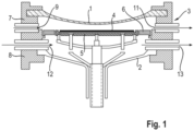
- the device shown for depositing an epitaxial layer on a substrate wafer comprises a deposition chamber 3 with an upper cover 1 and a lower cover 2 and upper and lower liners 7 and 8 which enclose a reaction space.
- Upper and lower lamp banks present outside the deposition chamber 3 are not shown. Using the radiant energy from the lamps, the deposition chamber is brought to the temperature necessary for gas phase deposition.
- a substrate disk 4 is placed on a susceptor 5, which is rotatably held from below by arms of a carrier. Beforehand, the substrate disk is placed on an end effector of a robot and closed by the robot moved to a storage position. A preheating ring 6 is arranged around the susceptor. The substrate disk 4 can be placed on the susceptor 5 by means of lifting pins which are passed through the susceptor 5 and lifted away from the susceptor 5 after coating.
- deposition gas slides through upper gas inlet openings 9, which are provided in the upper lining 7, into the deposition chamber 3 along a flow direction over the substrate disk to an upper gas outlet 11.
- lower gas inlet openings 12 and a lower gas outlet 13 can optionally be provided in order to direct a purge gas under the susceptor 5 to the lower gas outlet 13.
- the storage position for the robot is set such that the center of the substrate disk lies vertically above the center of the susceptor, there is a comparatively high probability that after the substrate disk has been deposited, its center will not be in the center of the susceptor.
- the reason for this is, in particular, thermal stresses that are released, causing the center of the substrate disk to be displaced from the intended position.
- the correction specification which also determines the storage position into which the robot moves a substrate disk before depositing it onto the susceptor.
- the correction specification is calculated for the first substrate disk that is to be coated after a chamber etching by averaging positional deviations of previously coated substrate disks, whereby only positional deviations of substrate disks of the first category are used for the calculation, i.e. of substrate disks that are themselves the first after a Chamber etches were coated.
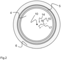
- Fig.2 shows a substrate disk 4, which is placed on a susceptor 5, so that the center 10 of the susceptor 5 and the center of the substrate disk 4 coincide.
- the substrate disk 4 lies concentric to the susceptor 5 and the preheating ring 6.
- the center of the substrate disk would lie at or near the middle position that was calculated for this category, depending on whether it belongs to the first or another category , for example on or near the first middle position 15 in the case of belonging to the first category or on or near the second middle position 14 in the case of belonging to another category.
- positions 14 and 15 are placed unrealistically far from the center 10 of the susceptor in order to be able to represent the invention.
- usual positional deviations are at a distance of no more than 1000 ⁇ m from the center 10 of the susceptor.
- the first middle position 15 is at a distance from the center 10 of the susceptor 5, which corresponds to the length of the vector 17.
- the second middle position 14 has a distance from the center 10 of the susceptor 5, which corresponds to the length of the vector 16. If the vector 16 or the vector 17 is shifted so that its beginning coincides with the center 10 of the susceptor, the tip of the vector points to the storage position into which the robot must move the substrate disk with its center so that an expected positional deviation is compensated for.
- the vector 17 therefore represents the correction specification for the robot in relation to the first substrate disk to be coated after chamber etching, the vector 16 represents the correction specification for the robot in relation to substrate disks of other categories.
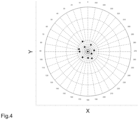
- Fig.3 and Fig.4 show for substrate wafers of the first category (number of coating processes preceding the last chamber etching is zero) or for substrate wafers of another category (number of coating processes preceding since the last chamber etching is 7). Positional deviations in a polar coordinate grid of the boron-doped substrate disks made of single-crystalline silicon with a diameter of 300 mm. The comparison of the distributions of the positional deviations shown makes it clear that the amount of the positional deviation is significantly more pronounced when it comes to substrate disks of the first category that were coated immediately after chamber etching.
Landscapes
- Chemical & Material Sciences (AREA)
- Engineering & Computer Science (AREA)
- General Chemical & Material Sciences (AREA)
- Chemical Kinetics & Catalysis (AREA)
- Materials Engineering (AREA)
- Metallurgy (AREA)
- Organic Chemistry (AREA)
- Mechanical Engineering (AREA)
- Crystallography & Structural Chemistry (AREA)
- Robotics (AREA)
- Chemical Vapour Deposition (AREA)
- Container, Conveyance, Adherence, Positioning, Of Wafer (AREA)
Priority Applications (8)
| Application Number | Priority Date | Filing Date | Title |
|---|---|---|---|
| EP21167990.7A EP4075488B1 (de) | 2021-04-13 | 2021-04-13 | Verfahren zum herstellen von halbleiterscheiben mit aus der gasphase abgeschiedener epitaktischer schicht in einer abscheidekammer |
| IL307321A IL307321B1 (he) | 2021-04-13 | 2022-03-28 | תהליך לייצור פרוסות מוליכות למחצה עם שכבה אפיטקסיאלית שהושקעה מפאזת גז בתא שיקוע |
| PCT/EP2022/058094 WO2022218678A1 (de) | 2021-04-13 | 2022-03-28 | Verfahren zum herstellen von halbleiterscheiben mit aus der gasphase abgeschiedener epitaktischer schicht in einer abscheidekammer |
| CN202280027831.0A CN117280454A (zh) | 2021-04-13 | 2022-03-28 | 在沉积室中制备具有由气相沉积的外延层的半导体晶圆的工艺 |
| KR1020237038943A KR102969957B1 (ko) | 2021-04-13 | 2022-03-28 | 증착 챔버에서 기체상으로부터 증착된 에피택셜 층을 갖는 반도체 웨이퍼를 제조하는 프로세스 |
| US18/554,221 US12662751B2 (en) | 2021-04-13 | 2022-03-28 | Process for manufacturing semiconductor wafers containing a gas-phase epitaxial layer in a deposition chamber |
| JP2023562281A JP7567067B2 (ja) | 2021-04-13 | 2022-03-28 | 堆積チャンバにおいて気相から堆積されるエピタキシャル層を有する半導体ウェーハを製造するためのプロセス |
| TW111112651A TWI801190B (zh) | 2021-04-13 | 2022-03-31 | 在沉積室中製備具有由氣相沉積的磊晶層的半導體晶圓的方法 |
Applications Claiming Priority (1)
| Application Number | Priority Date | Filing Date | Title |
|---|---|---|---|
| EP21167990.7A EP4075488B1 (de) | 2021-04-13 | 2021-04-13 | Verfahren zum herstellen von halbleiterscheiben mit aus der gasphase abgeschiedener epitaktischer schicht in einer abscheidekammer |
Publications (2)
| Publication Number | Publication Date |
|---|---|
| EP4075488A1 EP4075488A1 (de) | 2022-10-19 |
| EP4075488B1 true EP4075488B1 (de) | 2024-02-28 |
Family
ID=75497823
Family Applications (1)
| Application Number | Title | Priority Date | Filing Date |
|---|---|---|---|
| EP21167990.7A Active EP4075488B1 (de) | 2021-04-13 | 2021-04-13 | Verfahren zum herstellen von halbleiterscheiben mit aus der gasphase abgeschiedener epitaktischer schicht in einer abscheidekammer |
Country Status (8)
| Country | Link |
|---|---|
| US (1) | US12662751B2 (he) |
| EP (1) | EP4075488B1 (he) |
| JP (1) | JP7567067B2 (he) |
| KR (1) | KR102969957B1 (he) |
| CN (1) | CN117280454A (he) |
| IL (1) | IL307321B1 (he) |
| TW (1) | TWI801190B (he) |
| WO (1) | WO2022218678A1 (he) |
Family Cites Families (11)
| Publication number | Priority date | Publication date | Assignee | Title |
|---|---|---|---|---|
| JP3437118B2 (ja) * | 1999-04-23 | 2003-08-18 | 東芝機械株式会社 | ウエーハ加熱装置及びその制御方法 |
| JP2002261154A (ja) | 2001-03-02 | 2002-09-13 | Anelva Corp | 基板処理装置における基板のアライメント方法及び基板処理装置 |
| JP4502199B2 (ja) * | 2004-10-21 | 2010-07-14 | ルネサスエレクトロニクス株式会社 | エッチング装置およびエッチング方法 |
| JP2009140188A (ja) | 2007-12-05 | 2009-06-25 | Fujitsu Ltd | 位置教示方法、位置教示プログラムおよび位置教示装置 |
| KR101380179B1 (ko) * | 2011-09-30 | 2014-03-31 | 가부시키가이샤 뉴플레어 테크놀로지 | 성막 장치 및 성막 방법 |
| JP5704461B2 (ja) * | 2012-02-24 | 2015-04-22 | 信越半導体株式会社 | 枚葉式エピタキシャルウェーハ製造装置およびそれを用いたエピタキシャルウェーハの製造方法 |
| US9570334B2 (en) * | 2015-03-31 | 2017-02-14 | Taiwan Semiconductor Manufacturing Co., Ltd. | Method and system for positioning wafer in semiconductor manufacturing fabrication |
| JP6315285B2 (ja) | 2015-04-29 | 2018-04-25 | 信越半導体株式会社 | エピタキシャルウェーハの製造方法及び気相成長装置 |
| JP2018525527A (ja) * | 2015-08-18 | 2018-09-06 | ビーコ・インストゥルメンツ・インコーポレイテッド | 化学気相蒸着システム及びプロセスにおいて熱均一性を向上させるプロセス特異的ウェハーキャリアー補正 |
| DE102015225663A1 (de) | 2015-12-17 | 2017-06-22 | Siltronic Ag | Verfahren zum epitaktischen Beschichten von Halbleiterscheiben und Halbleiterscheibe |
| JP7135841B2 (ja) * | 2018-12-25 | 2022-09-13 | 株式会社Sumco | ウェーハ移載装置、気相成長装置、ウェーハ移載方法およびエピタキシャルシリコンウェーハの製造方法 |
-
2021
- 2021-04-13 EP EP21167990.7A patent/EP4075488B1/de active Active
-
2022
- 2022-03-28 WO PCT/EP2022/058094 patent/WO2022218678A1/de not_active Ceased
- 2022-03-28 IL IL307321A patent/IL307321B1/he unknown
- 2022-03-28 CN CN202280027831.0A patent/CN117280454A/zh active Pending
- 2022-03-28 US US18/554,221 patent/US12662751B2/en active Active
- 2022-03-28 JP JP2023562281A patent/JP7567067B2/ja active Active
- 2022-03-28 KR KR1020237038943A patent/KR102969957B1/ko active Active
- 2022-03-31 TW TW111112651A patent/TWI801190B/zh active
Also Published As
| Publication number | Publication date |
|---|---|
| TW202239999A (zh) | 2022-10-16 |
| TWI801190B (zh) | 2023-05-01 |
| KR20230169316A (ko) | 2023-12-15 |
| KR102969957B1 (ko) | 2026-05-27 |
| EP4075488A1 (de) | 2022-10-19 |
| CN117280454A (zh) | 2023-12-22 |
| IL307321A (he) | 2023-11-01 |
| IL307321B1 (he) | 2026-07-01 |
| JP7567067B2 (ja) | 2024-10-15 |
| US12662751B2 (en) | 2026-06-23 |
| US20240117523A1 (en) | 2024-04-11 |
| JP2024516121A (ja) | 2024-04-12 |
| WO2022218678A1 (de) | 2022-10-20 |
Similar Documents
| Publication | Publication Date | Title |
|---|---|---|
| DE69426679T2 (de) | Vorrichtung und Verfahren zur Sicherstellung der Hitzeübertragung auf BZW von einem ganzen Substrat während der Bearbeitung eines Halbleiterbauteils | |
| DE69635972T2 (de) | Plasma-Ätz-Verfahren | |
| DE69130293T2 (de) | Minimierung der partikelerzeugung in cvd-reaktoren und verfahren | |
| DE3877085T2 (de) | Entfernen von resistschichten. | |
| EP3721469B1 (de) | Verfahren zum abscheiden einer epitaktischen schicht auf einer vorderseite einer halbleiterscheibe und vorrichtung zur durchführung des verfahrens | |
| DE69210942T2 (de) | Halbleiterherstellung | |
| DE69520846T2 (de) | Einkristalliner Hableiterträger | |
| DE69118228T2 (de) | Klemmechanismus für physikalische Dampfniederschlagvorrichtung | |
| DE202010015933U1 (de) | Eine Randringanordnung für Plasmaätzkammern | |
| DE3103177A1 (de) | Verfahren zum herstellen von polysiliziumstrukturen bis in den 1 (my)m-bereich auf integrierte halbleiterschaltungen enthaltenden substraten durch plasmaaetzen | |
| DE112016003399T5 (de) | Verfahren zur Vorbereitung eines Reaktorneustarts zur Herstellung eines epitaktischen Wafers | |
| EP0089382B1 (de) | Plasmareaktor und seine Anwendung beim Ätzen und Beschichten von Substraten | |
| DE112008003535T5 (de) | Suszeptor für das epitaxiale Wachstum | |
| EP3475472A1 (de) | Verfahren und vorrichtung zur herstellung von beschichteten halbleiterscheiben | |
| DE102019207772A1 (de) | Verfahren zum Abscheiden einer epitaktischen Schicht auf einer Vorderseite einer Halbleiterscheibe und Vorrichtung zur Durchführung des Verfahrens | |
| DE1621394A1 (de) | Verfahren und Vorrichtung zum Erhitzen und/oder Beschichten von Werkstuecken | |
| DE2432719A1 (de) | Verfahren zum erzeugen von feinen strukturen aus aufdampfbaren materialien auf einer unterlage | |
| DE102017203255B4 (de) | Reaktor zur Verwendung bei einem System einer chemischen Dampfabscheidung und Verfahren zum Betreiben eines Systems einer chemischen Dampfabscheidung | |
| EP1127176B1 (de) | Vorrichtung zum herstellen und bearbeiten von halbleitersubstraten | |
| EP4075488A1 (de) | Verfahren zum herstellen von halbleiterscheiben mit aus der gasphase abgeschiedener epitaktischer schicht in einer abscheidekammer | |
| EP4075489B1 (de) | Verfahren zum herstellen von halbleiterscheiben mit aus der gasphase abgeschiedener epitaktischer schicht in einer abscheidekammer | |
| DE102014209466B4 (de) | Trockenätzungsvorrichtung und Elektrode davon | |
| WO2022218738A1 (de) | Verfahren zum herstellen von halbleiterscheiben mit aus der gasphase abgeschiedener epitaktischer schicht in einer abscheidekammer | |
| DE3242855A1 (de) | Verfahren und vorrichtung zur konturierung der dicke von aufgespruehten schichten | |
| WO1995013525A1 (de) | Verfahren zum erzeugen wenigstens einer ausnehmung in einer oberfläche eines substrats, vorrichtung zur durchführung des verfahrens und verwendung des verfahrensprodukts |
Legal Events
| Date | Code | Title | Description |
|---|---|---|---|
| PUAI | Public reference made under article 153(3) epc to a published international application that has entered the european phase |
Free format text: ORIGINAL CODE: 0009012 |
|
| STAA | Information on the status of an ep patent application or granted ep patent |
Free format text: STATUS: THE APPLICATION HAS BEEN PUBLISHED |
|
| AK | Designated contracting states |
Kind code of ref document: A1 Designated state(s): AL AT BE BG CH CY CZ DE DK EE ES FI FR GB GR HR HU IE IS IT LI LT LU LV MC MK MT NL NO PL PT RO RS SE SI SK SM TR |
|
| STAA | Information on the status of an ep patent application or granted ep patent |
Free format text: STATUS: REQUEST FOR EXAMINATION WAS MADE |
|
| 17P | Request for examination filed |
Effective date: 20230404 |
|
| RBV | Designated contracting states (corrected) |
Designated state(s): AL AT BE BG CH CY CZ DE DK EE ES FI FR GB GR HR HU IE IS IT LI LT LU LV MC MK MT NL NO PL PT RO RS SE SI SK SM TR |
|
| GRAP | Despatch of communication of intention to grant a patent |
Free format text: ORIGINAL CODE: EPIDOSNIGR1 |
|
| STAA | Information on the status of an ep patent application or granted ep patent |
Free format text: STATUS: GRANT OF PATENT IS INTENDED |
|
| INTG | Intention to grant announced |
Effective date: 20231006 |
|
| GRAS | Grant fee paid |
Free format text: ORIGINAL CODE: EPIDOSNIGR3 |
|
| GRAA | (expected) grant |
Free format text: ORIGINAL CODE: 0009210 |
|
| STAA | Information on the status of an ep patent application or granted ep patent |
Free format text: STATUS: THE PATENT HAS BEEN GRANTED |
|
| AK | Designated contracting states |
Kind code of ref document: B1 Designated state(s): AL AT BE BG CH CY CZ DE DK EE ES FI FR GB GR HR HU IE IS IT LI LT LU LV MC MK MT NL NO PL PT RO RS SE SI SK SM TR |
|
| REG | Reference to a national code |
Ref country code: GB Ref legal event code: FG4D Free format text: NOT ENGLISH |
|
| REG | Reference to a national code |
Ref country code: CH Ref legal event code: EP |
|
| REG | Reference to a national code |
Ref country code: DE Ref legal event code: R096 Ref document number: 502021002799 Country of ref document: DE |
|
| REG | Reference to a national code |
Ref country code: IE Ref legal event code: FG4D Free format text: LANGUAGE OF EP DOCUMENT: GERMAN |
|
| REG | Reference to a national code |
Ref country code: LT Ref legal event code: MG9D |
|
| PG25 | Lapsed in a contracting state [announced via postgrant information from national office to epo] |
Ref country code: IS Free format text: LAPSE BECAUSE OF FAILURE TO SUBMIT A TRANSLATION OF THE DESCRIPTION OR TO PAY THE FEE WITHIN THE PRESCRIBED TIME-LIMIT Effective date: 20240628 |
|
| REG | Reference to a national code |
Ref country code: NL Ref legal event code: MP Effective date: 20240228 |
|
| PG25 | Lapsed in a contracting state [announced via postgrant information from national office to epo] |
Ref country code: LT Free format text: LAPSE BECAUSE OF FAILURE TO SUBMIT A TRANSLATION OF THE DESCRIPTION OR TO PAY THE FEE WITHIN THE PRESCRIBED TIME-LIMIT Effective date: 20240228 |
|
| PG25 | Lapsed in a contracting state [announced via postgrant information from national office to epo] |
Ref country code: GR Free format text: LAPSE BECAUSE OF FAILURE TO SUBMIT A TRANSLATION OF THE DESCRIPTION OR TO PAY THE FEE WITHIN THE PRESCRIBED TIME-LIMIT Effective date: 20240529 |
|
| PG25 | Lapsed in a contracting state [announced via postgrant information from national office to epo] |
Ref country code: RS Free format text: LAPSE BECAUSE OF FAILURE TO SUBMIT A TRANSLATION OF THE DESCRIPTION OR TO PAY THE FEE WITHIN THE PRESCRIBED TIME-LIMIT Effective date: 20240528 Ref country code: HR Free format text: LAPSE BECAUSE OF FAILURE TO SUBMIT A TRANSLATION OF THE DESCRIPTION OR TO PAY THE FEE WITHIN THE PRESCRIBED TIME-LIMIT Effective date: 20240228 Ref country code: NL Free format text: LAPSE BECAUSE OF FAILURE TO SUBMIT A TRANSLATION OF THE DESCRIPTION OR TO PAY THE FEE WITHIN THE PRESCRIBED TIME-LIMIT Effective date: 20240228 |
|
| PG25 | Lapsed in a contracting state [announced via postgrant information from national office to epo] |
Ref country code: ES Free format text: LAPSE BECAUSE OF FAILURE TO SUBMIT A TRANSLATION OF THE DESCRIPTION OR TO PAY THE FEE WITHIN THE PRESCRIBED TIME-LIMIT Effective date: 20240228 |
|
| PG25 | Lapsed in a contracting state [announced via postgrant information from national office to epo] |
Ref country code: RS Free format text: LAPSE BECAUSE OF FAILURE TO SUBMIT A TRANSLATION OF THE DESCRIPTION OR TO PAY THE FEE WITHIN THE PRESCRIBED TIME-LIMIT Effective date: 20240528 Ref country code: NO Free format text: LAPSE BECAUSE OF FAILURE TO SUBMIT A TRANSLATION OF THE DESCRIPTION OR TO PAY THE FEE WITHIN THE PRESCRIBED TIME-LIMIT Effective date: 20240528 Ref country code: NL Free format text: LAPSE BECAUSE OF FAILURE TO SUBMIT A TRANSLATION OF THE DESCRIPTION OR TO PAY THE FEE WITHIN THE PRESCRIBED TIME-LIMIT Effective date: 20240228 Ref country code: LT Free format text: LAPSE BECAUSE OF FAILURE TO SUBMIT A TRANSLATION OF THE DESCRIPTION OR TO PAY THE FEE WITHIN THE PRESCRIBED TIME-LIMIT Effective date: 20240228 Ref country code: IS Free format text: LAPSE BECAUSE OF FAILURE TO SUBMIT A TRANSLATION OF THE DESCRIPTION OR TO PAY THE FEE WITHIN THE PRESCRIBED TIME-LIMIT Effective date: 20240628 Ref country code: HR Free format text: LAPSE BECAUSE OF FAILURE TO SUBMIT A TRANSLATION OF THE DESCRIPTION OR TO PAY THE FEE WITHIN THE PRESCRIBED TIME-LIMIT Effective date: 20240228 Ref country code: GR Free format text: LAPSE BECAUSE OF FAILURE TO SUBMIT A TRANSLATION OF THE DESCRIPTION OR TO PAY THE FEE WITHIN THE PRESCRIBED TIME-LIMIT Effective date: 20240529 Ref country code: FI Free format text: LAPSE BECAUSE OF FAILURE TO SUBMIT A TRANSLATION OF THE DESCRIPTION OR TO PAY THE FEE WITHIN THE PRESCRIBED TIME-LIMIT Effective date: 20240228 Ref country code: ES Free format text: LAPSE BECAUSE OF FAILURE TO SUBMIT A TRANSLATION OF THE DESCRIPTION OR TO PAY THE FEE WITHIN THE PRESCRIBED TIME-LIMIT Effective date: 20240228 Ref country code: BG Free format text: LAPSE BECAUSE OF FAILURE TO SUBMIT A TRANSLATION OF THE DESCRIPTION OR TO PAY THE FEE WITHIN THE PRESCRIBED TIME-LIMIT Effective date: 20240228 |
|
| PG25 | Lapsed in a contracting state [announced via postgrant information from national office to epo] |
Ref country code: PL Free format text: LAPSE BECAUSE OF FAILURE TO SUBMIT A TRANSLATION OF THE DESCRIPTION OR TO PAY THE FEE WITHIN THE PRESCRIBED TIME-LIMIT Effective date: 20240228 Ref country code: PT Free format text: LAPSE BECAUSE OF FAILURE TO SUBMIT A TRANSLATION OF THE DESCRIPTION OR TO PAY THE FEE WITHIN THE PRESCRIBED TIME-LIMIT Effective date: 20240628 |
|
| PG25 | Lapsed in a contracting state [announced via postgrant information from national office to epo] |
Ref country code: SE Free format text: LAPSE BECAUSE OF FAILURE TO SUBMIT A TRANSLATION OF THE DESCRIPTION OR TO PAY THE FEE WITHIN THE PRESCRIBED TIME-LIMIT Effective date: 20240228 Ref country code: PT Free format text: LAPSE BECAUSE OF FAILURE TO SUBMIT A TRANSLATION OF THE DESCRIPTION OR TO PAY THE FEE WITHIN THE PRESCRIBED TIME-LIMIT Effective date: 20240628 Ref country code: PL Free format text: LAPSE BECAUSE OF FAILURE TO SUBMIT A TRANSLATION OF THE DESCRIPTION OR TO PAY THE FEE WITHIN THE PRESCRIBED TIME-LIMIT Effective date: 20240228 Ref country code: LV Free format text: LAPSE BECAUSE OF FAILURE TO SUBMIT A TRANSLATION OF THE DESCRIPTION OR TO PAY THE FEE WITHIN THE PRESCRIBED TIME-LIMIT Effective date: 20240228 |
|
| PG25 | Lapsed in a contracting state [announced via postgrant information from national office to epo] |
Ref country code: DK Free format text: LAPSE BECAUSE OF FAILURE TO SUBMIT A TRANSLATION OF THE DESCRIPTION OR TO PAY THE FEE WITHIN THE PRESCRIBED TIME-LIMIT Effective date: 20240228 |
|
| PG25 | Lapsed in a contracting state [announced via postgrant information from national office to epo] |
Ref country code: SM Free format text: LAPSE BECAUSE OF FAILURE TO SUBMIT A TRANSLATION OF THE DESCRIPTION OR TO PAY THE FEE WITHIN THE PRESCRIBED TIME-LIMIT Effective date: 20240228 |
|
| PG25 | Lapsed in a contracting state [announced via postgrant information from national office to epo] |
Ref country code: EE Free format text: LAPSE BECAUSE OF FAILURE TO SUBMIT A TRANSLATION OF THE DESCRIPTION OR TO PAY THE FEE WITHIN THE PRESCRIBED TIME-LIMIT Effective date: 20240228 Ref country code: CZ Free format text: LAPSE BECAUSE OF FAILURE TO SUBMIT A TRANSLATION OF THE DESCRIPTION OR TO PAY THE FEE WITHIN THE PRESCRIBED TIME-LIMIT Effective date: 20240228 |
|
| PG25 | Lapsed in a contracting state [announced via postgrant information from national office to epo] |
Ref country code: SK Free format text: LAPSE BECAUSE OF FAILURE TO SUBMIT A TRANSLATION OF THE DESCRIPTION OR TO PAY THE FEE WITHIN THE PRESCRIBED TIME-LIMIT Effective date: 20240228 |
|
| PG25 | Lapsed in a contracting state [announced via postgrant information from national office to epo] |
Ref country code: SM Free format text: LAPSE BECAUSE OF FAILURE TO SUBMIT A TRANSLATION OF THE DESCRIPTION OR TO PAY THE FEE WITHIN THE PRESCRIBED TIME-LIMIT Effective date: 20240228 Ref country code: SK Free format text: LAPSE BECAUSE OF FAILURE TO SUBMIT A TRANSLATION OF THE DESCRIPTION OR TO PAY THE FEE WITHIN THE PRESCRIBED TIME-LIMIT Effective date: 20240228 Ref country code: RO Free format text: LAPSE BECAUSE OF FAILURE TO SUBMIT A TRANSLATION OF THE DESCRIPTION OR TO PAY THE FEE WITHIN THE PRESCRIBED TIME-LIMIT Effective date: 20240228 Ref country code: EE Free format text: LAPSE BECAUSE OF FAILURE TO SUBMIT A TRANSLATION OF THE DESCRIPTION OR TO PAY THE FEE WITHIN THE PRESCRIBED TIME-LIMIT Effective date: 20240228 Ref country code: DK Free format text: LAPSE BECAUSE OF FAILURE TO SUBMIT A TRANSLATION OF THE DESCRIPTION OR TO PAY THE FEE WITHIN THE PRESCRIBED TIME-LIMIT Effective date: 20240228 Ref country code: CZ Free format text: LAPSE BECAUSE OF FAILURE TO SUBMIT A TRANSLATION OF THE DESCRIPTION OR TO PAY THE FEE WITHIN THE PRESCRIBED TIME-LIMIT Effective date: 20240228 |
|
| PG25 | Lapsed in a contracting state [announced via postgrant information from national office to epo] |
Ref country code: MC Free format text: LAPSE BECAUSE OF FAILURE TO SUBMIT A TRANSLATION OF THE DESCRIPTION OR TO PAY THE FEE WITHIN THE PRESCRIBED TIME-LIMIT Effective date: 20240228 |
|
| PG25 | Lapsed in a contracting state [announced via postgrant information from national office to epo] |
Ref country code: MC Free format text: LAPSE BECAUSE OF FAILURE TO SUBMIT A TRANSLATION OF THE DESCRIPTION OR TO PAY THE FEE WITHIN THE PRESCRIBED TIME-LIMIT Effective date: 20240228 |
|
| REG | Reference to a national code |
Ref country code: DE Ref legal event code: R097 Ref document number: 502021002799 Country of ref document: DE Ref country code: CH Ref legal event code: PL |
|
| PG25 | Lapsed in a contracting state [announced via postgrant information from national office to epo] |
Ref country code: LU Free format text: LAPSE BECAUSE OF NON-PAYMENT OF DUE FEES Effective date: 20240413 |
|
| REG | Reference to a national code |
Ref country code: BE Ref legal event code: MM Effective date: 20240430 |
|
| PG25 | Lapsed in a contracting state [announced via postgrant information from national office to epo] |
Ref country code: LU Free format text: LAPSE BECAUSE OF NON-PAYMENT OF DUE FEES Effective date: 20240413 |
|
| PLBE | No opposition filed within time limit |
Free format text: ORIGINAL CODE: 0009261 |
|
| STAA | Information on the status of an ep patent application or granted ep patent |
Free format text: STATUS: NO OPPOSITION FILED WITHIN TIME LIMIT |
|
| PG25 | Lapsed in a contracting state [announced via postgrant information from national office to epo] |
Ref country code: BE Free format text: LAPSE BECAUSE OF NON-PAYMENT OF DUE FEES Effective date: 20240430 |
|
| PG25 | Lapsed in a contracting state [announced via postgrant information from national office to epo] |
Ref country code: FR Free format text: LAPSE BECAUSE OF NON-PAYMENT OF DUE FEES Effective date: 20240428 |
|
| PG25 | Lapsed in a contracting state [announced via postgrant information from national office to epo] |
Ref country code: FR Free format text: LAPSE BECAUSE OF NON-PAYMENT OF DUE FEES Effective date: 20240428 Ref country code: BE Free format text: LAPSE BECAUSE OF NON-PAYMENT OF DUE FEES Effective date: 20240430 Ref country code: CH Free format text: LAPSE BECAUSE OF NON-PAYMENT OF DUE FEES Effective date: 20240430 |
|
| 26N | No opposition filed |
Effective date: 20241129 |
|
| PG25 | Lapsed in a contracting state [announced via postgrant information from national office to epo] |
Ref country code: SI Free format text: LAPSE BECAUSE OF FAILURE TO SUBMIT A TRANSLATION OF THE DESCRIPTION OR TO PAY THE FEE WITHIN THE PRESCRIBED TIME-LIMIT Effective date: 20240228 |
|
| PGFP | Annual fee paid to national office [announced via postgrant information from national office to epo] |
Ref country code: AT Payment date: 20250721 Year of fee payment: 5 |
|
| PG25 | Lapsed in a contracting state [announced via postgrant information from national office to epo] |
Ref country code: CY Free format text: LAPSE BECAUSE OF FAILURE TO SUBMIT A TRANSLATION OF THE DESCRIPTION OR TO PAY THE FEE WITHIN THE PRESCRIBED TIME-LIMIT; INVALID AB INITIO Effective date: 20210413 |
|
| PG25 | Lapsed in a contracting state [announced via postgrant information from national office to epo] |
Ref country code: HU Free format text: LAPSE BECAUSE OF FAILURE TO SUBMIT A TRANSLATION OF THE DESCRIPTION OR TO PAY THE FEE WITHIN THE PRESCRIBED TIME-LIMIT; INVALID AB INITIO Effective date: 20210413 |
|
| REG | Reference to a national code |
Ref country code: DE Ref legal event code: R079 Ref document number: 502021002799 Country of ref document: DE Free format text: PREVIOUS MAIN CLASS: H01L0021680000 Ipc: H10P0072500000 |
|
| GBPC | Gb: european patent ceased through non-payment of renewal fee |
Effective date: 20250413 |
|
| PG25 | Lapsed in a contracting state [announced via postgrant information from national office to epo] |
Ref country code: GB Free format text: LAPSE BECAUSE OF NON-PAYMENT OF DUE FEES Effective date: 20250413 |
|
| PG25 | Lapsed in a contracting state [announced via postgrant information from national office to epo] |
Ref country code: TR Free format text: LAPSE BECAUSE OF FAILURE TO SUBMIT A TRANSLATION OF THE DESCRIPTION OR TO PAY THE FEE WITHIN THE PRESCRIBED TIME-LIMIT Effective date: 20240228 |
|
| PGFP | Annual fee paid to national office [announced via postgrant information from national office to epo] |
Ref country code: IT Payment date: 20260422 Year of fee payment: 6 |
|
| PGFP | Annual fee paid to national office [announced via postgrant information from national office to epo] |
Ref country code: DE Payment date: 20260421 Year of fee payment: 6 |
|
| PGFP | Annual fee paid to national office [announced via postgrant information from national office to epo] |
Ref country code: IE Payment date: 20260417 Year of fee payment: 6 |