EP4064367B1 - Structure de contact de passivation de couche d'oxyde à effet tunnel partiel de cellule photovoltaïque et module photovoltaïque - Google Patents
Structure de contact de passivation de couche d'oxyde à effet tunnel partiel de cellule photovoltaïque et module photovoltaïque Download PDFInfo
- Publication number
- EP4064367B1 EP4064367B1 EP19953507.1A EP19953507A EP4064367B1 EP 4064367 B1 EP4064367 B1 EP 4064367B1 EP 19953507 A EP19953507 A EP 19953507A EP 4064367 B1 EP4064367 B1 EP 4064367B1
- Authority
- EP
- European Patent Office
- Prior art keywords
- tunnel oxide
- oxide layer
- polysilicon film
- region
- cell
- Prior art date
- Legal status (The legal status is an assumption and is not a legal conclusion. Google has not performed a legal analysis and makes no representation as to the accuracy of the status listed.)
- Active
Links
Images
Classifications
-
- H—ELECTRICITY
- H10—SEMICONDUCTOR DEVICES; ELECTRIC SOLID-STATE DEVICES NOT OTHERWISE PROVIDED FOR
- H10F—INORGANIC SEMICONDUCTOR DEVICES SENSITIVE TO INFRARED RADIATION, LIGHT, ELECTROMAGNETIC RADIATION OF SHORTER WAVELENGTH OR CORPUSCULAR RADIATION
- H10F77/00—Constructional details of devices covered by this subclass
- H10F77/20—Electrodes
- H10F77/206—Electrodes for devices having potential barriers
- H10F77/211—Electrodes for devices having potential barriers for photovoltaic cells
-
- H—ELECTRICITY
- H10—SEMICONDUCTOR DEVICES; ELECTRIC SOLID-STATE DEVICES NOT OTHERWISE PROVIDED FOR
- H10F—INORGANIC SEMICONDUCTOR DEVICES SENSITIVE TO INFRARED RADIATION, LIGHT, ELECTROMAGNETIC RADIATION OF SHORTER WAVELENGTH OR CORPUSCULAR RADIATION
- H10F10/00—Individual photovoltaic cells, e.g. solar cells
- H10F10/10—Individual photovoltaic cells, e.g. solar cells having potential barriers
- H10F10/14—Photovoltaic cells having only PN homojunction potential barriers
- H10F10/148—Double-emitter photovoltaic cells, e.g. bifacial photovoltaic cells
-
- H—ELECTRICITY
- H10—SEMICONDUCTOR DEVICES; ELECTRIC SOLID-STATE DEVICES NOT OTHERWISE PROVIDED FOR
- H10F—INORGANIC SEMICONDUCTOR DEVICES SENSITIVE TO INFRARED RADIATION, LIGHT, ELECTROMAGNETIC RADIATION OF SHORTER WAVELENGTH OR CORPUSCULAR RADIATION
- H10F10/00—Individual photovoltaic cells, e.g. solar cells
- H10F10/10—Individual photovoltaic cells, e.g. solar cells having potential barriers
- H10F10/14—Photovoltaic cells having only PN homojunction potential barriers
-
- H—ELECTRICITY
- H10—SEMICONDUCTOR DEVICES; ELECTRIC SOLID-STATE DEVICES NOT OTHERWISE PROVIDED FOR
- H10F—INORGANIC SEMICONDUCTOR DEVICES SENSITIVE TO INFRARED RADIATION, LIGHT, ELECTROMAGNETIC RADIATION OF SHORTER WAVELENGTH OR CORPUSCULAR RADIATION
- H10F77/00—Constructional details of devices covered by this subclass
- H10F77/30—Coatings
- H10F77/306—Coatings for devices having potential barriers
- H10F77/311—Coatings for devices having potential barriers for photovoltaic cells
-
- H—ELECTRICITY
- H10—SEMICONDUCTOR DEVICES; ELECTRIC SOLID-STATE DEVICES NOT OTHERWISE PROVIDED FOR
- H10F—INORGANIC SEMICONDUCTOR DEVICES SENSITIVE TO INFRARED RADIATION, LIGHT, ELECTROMAGNETIC RADIATION OF SHORTER WAVELENGTH OR CORPUSCULAR RADIATION
- H10F77/00—Constructional details of devices covered by this subclass
- H10F77/93—Interconnections
- H10F77/933—Interconnections for devices having potential barriers
- H10F77/935—Interconnections for devices having potential barriers for photovoltaic devices or modules
Definitions
- the present disclosure relates to the technical field of photovoltaic cells, in particular to a structure of partial tunnel oxide passivated contact for a photovoltaic cell and a photovoltaic module.
- Tunnel oxide passivated contact is capable to suppress the recombination at the metallic contact region.
- a silicon-based film has strong absorption on sunlight, which restricts application of the tunnel oxide passivated contact on a front surface of the crystalline silicon solar cells. Hence, the conversion efficiency of the crystalline silicon solar cells is hindered from further improvement.
- CN110137274 relates to a preparation method of a double-sided passivation contact P-type high-efficiency battery.
- the preparation method comprises the following steps: S1, cleaning and texturing; S2,preparing frontal polysilicon; S3, preparing a mask; S4, etching; S5, diffusion; S6, cleaning; S7, annealing; S8, preparing a back polysilicon layer; S9, preparing a front SiNx antireflection layer;and S10. Printing.
- the invention also discloses the double-sided passivation contact P-type high-efficiency battery comprising P-type monocrystalline silicon.
- An N-type emitter is provided with a front ultra-thin silicon oxide layer far from the P-type monocrystalline silicon.
- a back ultra-thin silicon oxide layer is arranged on the back surface of the P-type monocrystalline silicon.
- the contact structure is passivated by using the tunnel oxide layer on the front and back surfaces of the battery so as to have great surface passivation effect.
- the silicon surface is passivated exactly under the front metal gate line and the back aluminum back field so as to avoid direct contact between the metal and the silicon base, reduce the surface recombination and improve the conversion efficiency of the battery.
- An objective of the present disclosure is to provide a structure of partial tunnel oxide passivated contact for a photovoltaic cell and a photovoltaic module.
- the contact structure and the photovoltaic module which are compatible with conventional mass production techniques of crystalline-silicon cells, thus can be put into mass production quickly, and can lead to fast improvement of efficiency and fast reduction of costs.
- the invention is set out in the appended set of claims.
- a structure of partial tunnel oxide passivated contact for a photovoltaic cell includes a cell body, a first tunnel oxide layer disposed on a surface of the cell body, and a first polysilicon film disposed on a surface of the tunnel oxide layer, where the surface of the cell body has a region for passivated contact and a region for light absorption, the first tunnel oxide layer is disposed in the region for passivated contact, and a projection of the first polysilicon film on the surface of the cell body is located in the region for passivated contact.
- the structure further includes a second tunnel oxide layer and a second polysilicon film that are disposed between the first tunnel oxide layer and the cell body layer, where both a projection of the second tunnel oxide layer and a projection of the second polysilicon film on the cell body cover the region for passivated contact and the region for light absorption.
- both a thickness of the first tunnel oxide layer and a thickness of the second tunnel oxide layer range from 0.5nm to 5nm.
- a thickness of the first polysilicon film ranges from 20nm to 300nm.
- a thickness of the second polysilicon film ranges from 5nm to 50nm.
- a thickness of the first tunnel oxide layer is equal to a thickness of the second tunnel oxide layer.
- the cell body is of a single-sided cell or a double-sided cell.
- a photovoltaic module is further provided according to an embodiment of the present disclosure.
- the photovoltaic module includes a cell body and the forgoing structure that is disposed on the cell body.
- the structure of partial tunnel oxide passivated contact for the photovoltaic cell and the photovoltaic module according to embodiments of the present disclosure have following advantages over conventional technology.
- the first tunnel oxide layer and the first polysilicon film merely cover the region for passivated contact, which improves a degree of passivation in such region, and suppress recombination at a surface of a cell.
- the first tunnel oxide layer and the first polysilicon film are not disposed in the region for light absorption, i.e., a region of non-metallic contact, which reduces blockage on sunlight and improves light absorption efficiency.
- the structure and the photovoltaic module are compatible with conventional mass production techniques of the crystalline-silicon cells, thus can be put into mass production quickly, and can lead to fast improvement of efficiency and fast reduction of costs.
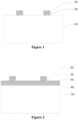
- Figure 1 is a schematic diagram showing a structure of partial tunnel oxide passivated contact for a photovoltaic cell according to an embodiment of the present disclosure.
- Figure 2 is a schematic diagram showing a structure of partial tunnel oxide passivated contact for a photovoltaic cell according to another embodiment of the present disclosure.
- a structure of partial tunnel oxide passivated contact for a photovoltaic cell includes a cell body 10, a first tunnel oxide layer 20 disposed on a surface of the cell body 10, and a first polysilicon film 30 disposed on a surface of the tunnel oxide layer.
- the surface of the cell body 10 includes a region for passivated contact and a region for light absorption.
- the first tunnel oxide layer 20 is disposed in the region for passivated contact, and a projection of the first polysilicon film 30 on the surface of the cell body 10 is located in the region for passivated contact.
- the first tunnel oxide layer 20 and the first polysilicon film 30 merely cover the region for passivated contact, which improves a degree of passivation in such region, and suppress recombination at a surface of a cell.
- the first tunnel oxide layer 20 and the first polysilicon film 30 are not disposed in the region for light absorption, i.e., a region of non-metallic contact, which reduces blockage on sunlight and improves light absorption efficiency.
- the structure and the photovoltaic module are compatible with conventional mass production techniques of the crystalline-silicon cells, thus can be put into mass production quickly, and can lead to fast improvement of efficiency and fast reduction of costs.
- passivation contact cover the whole front side. In comparison, only a region of metallic contact is covered according to embodiments of the present disclosure, and thereby efficiency of a cell is improved.
- the structure of partial tunnel oxide passivated contact for the photovoltaic cell further includes a second tunnel oxide layer 40 and a second polysilicon film 50, which are disposed between the first tunnel oxide layer 20 and the cell body 10. Both a projection of the second tunnel oxide layer 40 and a projection of the second polysilicon film 50 on the cell body 10 cover the region for passivated contact and the region for light absorption.
- doping concentration of the first polysilicon film 30 is greater than that of the second polysilicon film 50, which forms a "vertical conjunction" structure.
- the vertical conjunction in the passivated contact addresses incompatibility between complete passivation and light absorption, and incompatibility between the complete passivation and penetration damages due to the metallic electrode. Thereby, conversion efficiency of the cell is improved.
- a thickness of the tunnel oxide layer and a manner of fabrication of the tunnel oxide layer are not limited herein. Generally, a thickness of the first tunnel oxide layer 20 and a thickness of the second tunnel oxide layer 40 both range from 0.5nm to 5nm.
- a thickness of the silicon film of and a manner of depositing the silicon film are not limited herein. Generally, a thickness of the first polysilicon film 30 and a thickness of the second polysilicon film 50 both range from 20nm to 300nm.
- a thickness of the first tunnel oxide layer 20 is equal to a thickness of the second tunnel oxide layer 40.
- a thickness of the first polysilicon film 30 is equal to a thickness of the second polysilicon film 50.
- the cell body 10 may be a single-sided cell body 10 or a double-sided cell body 10.
- a process of fabricating the foregoing structure of partial tunnel oxide passivated contact for the photovoltaic cell is as follows.
- a process of fabricating the foregoing structure of partial tunnel oxide passivated contact for the photovoltaic cell is as follows.
- the above processes save a PECVD mask process when fabricating the structure of partial tunnel oxide passivated contact, and hence is simple.
- the above processes further save a laser etching process, and hence avoids damages on the silicon wafer substrate induced by a laser.
- the above processes can stop the etching on the polysilicon at the surface of the tunnel oxide layer, which protects the surface morphology of the silicon substrate and avoid re-texturing.
- the second foregoing process utilize the "vertical junction" structure in the passivated contact, which addresses incompatibility between complete passivation and light absorption and incompatibility between the complete passivation and penetration damages due to the metallic electrode. Thereby, conversion efficiency of the cell is improved.
- the second foregoing process save a PECVD mask process when fabricating the structure of partial tunnel oxide passivated contact, and hence is simple.
- the second foregoing process further save a laser etching process, and hence avoids damages induced by a laser on the ultra-thin passivated contact and the silicon wafer substrate.
- the second foregoing process can stop the etching on the polysilicon at the surface of the tunnel oxide layer, and can retain the ultra-thin passivated contact structure in the non-metallic contact region.
- a photovoltaic module is further provided according to embodiments of the present disclosure.
- the photovoltaic module includes a cell body and the foregoing structure of partial tunnel oxide passivated contact for the photovoltaic cell, and the structure is disposed on the cell body.
- the photovoltaic module including the forgoing structure has the same beneficial effects achieved by the forgoing structure. Hence, the beneficial effects are not repeated herein.
- the structure of partial tunnel oxide passivated contact for the photovoltaic cell and the photovoltaic module are provided according to embodiments of the present disclosure.
- the first tunnel oxide layer and the first polysilicon film merely cover the region for passivated contact, which improves a degree of passivation in such region, and suppress recombination at a surface of a cell.
- the first tunnel oxide layer and the first polysilicon film are not disposed in the region for light absorption, i.e., a region of non-metallic contact, which reduces blockage on sunlight and improves light absorption efficiency.
- the structure and the photovoltaic module are compatible with conventional mass production techniques of the crystalline-silicon cells, thus can be put into mass production quickly, and can lead to fast improvement of efficiency and fast reduction of costs.
Landscapes
- Photovoltaic Devices (AREA)
- Life Sciences & Earth Sciences (AREA)
- Engineering & Computer Science (AREA)
- Sustainable Energy (AREA)
- Sustainable Development (AREA)
Claims (7)
- Structure de contact passivé par oxyde tunnel partiel pour une cellule photovoltaïque, comprenant :un corps de cellule (10) ;une première couche d'oxyde tunnel (20) sur une surface du corps de cellule (10) ; etun premier film de polysilicium (30) sur une surface de la première couche d'oxyde tunnel (20) ;dans laquelle la surface du corps de cellule (10) a une région pour contact passivé et une région pour absorption de lumière, la première couche d'oxyde tunnel (20) est disposée dans la région pour contact passivé, et une projection du premier film de polysilicium (30) sur la surface du corps de cellule (10) est située dans la région pour contact passivé ;caractérisée en ce que la structure comprend en outre :une deuxième couche d'oxyde tunnel (40) sur la surface du corps de cellule (10) et un deuxième film de polysilicium (50) sur une surface de la deuxième couche d'oxyde tunnel (40), qui sont disposés entre la première couche d'oxyde tunnel (20) et le corps de cellule (10),dans laquelle tant une projection de la deuxième couche d'oxyde tunnel (40) qu'une projection du deuxième film de polysilicium (50) sur le corps de cellule (10) couvrent entièrement la région pour contact passivé et la région pour absorption de lumière.
- Structure selon la revendication 1, dans laquelle tant l'épaisseur de la première couche d'oxyde tunnel (20) que l'épaisseur de la deuxième couche d'oxyde tunnel (40) sont situées dans la plage allant de 0,5 nm à 5 nm.
- Structure selon la revendication 2, dans laquelle l'épaisseur du premier film de polysilicium (30) est située dans la plage allant de 20 nm à 300 nm.
- Structure selon la revendication 2, dans laquelle l'épaisseur du deuxième film de polysilicium (50) est située dans la plage allant de 20 nm à 300 nm.
- Structure selon la revendication 4, dans laquelle l'épaisseur de la première couche d'oxyde tunnel (20) est égale à l'épaisseur de la deuxième couche d'oxyde tunnel (40).
- Structure selon la revendication 5, dans laquelle le corps de cellule (10) est celui d'une cellule simple face ou d'une cellule double face.
- Module photovoltaïque comprenant :un corps de cellule (10) ; etla structure selon l'une quelconque des revendications 1 à 6,dans lequel la structure est disposée sur le corps de cellule (10).
Applications Claiming Priority (3)
| Application Number | Priority Date | Filing Date | Title |
|---|---|---|---|
| CN201911142103.0A CN110752261A (zh) | 2019-11-20 | 2019-11-20 | 一种光伏电池局部遂穿氧化层钝化接触结构及光伏组件 |
| CN201922019213.XU CN210866196U (zh) | 2019-11-20 | 2019-11-20 | 一种光伏电池局部隧穿氧化层钝化接触结构及光伏组件 |
| PCT/CN2019/129771 WO2021098018A1 (fr) | 2019-11-20 | 2019-12-30 | Structure de contact de passivation de couche d'oxyde à effet tunnel partiel de cellule photovoltaïque et module photovoltaïque |
Publications (4)
| Publication Number | Publication Date |
|---|---|
| EP4064367A1 EP4064367A1 (fr) | 2022-09-28 |
| EP4064367A4 EP4064367A4 (fr) | 2023-12-06 |
| EP4064367C0 EP4064367C0 (fr) | 2024-11-06 |
| EP4064367B1 true EP4064367B1 (fr) | 2024-11-06 |
Family
ID=75980220
Family Applications (1)
| Application Number | Title | Priority Date | Filing Date |
|---|---|---|---|
| EP19953507.1A Active EP4064367B1 (fr) | 2019-11-20 | 2019-12-30 | Structure de contact de passivation de couche d'oxyde à effet tunnel partiel de cellule photovoltaïque et module photovoltaïque |
Country Status (4)
| Country | Link |
|---|---|
| US (1) | US20230006086A1 (fr) |
| EP (1) | EP4064367B1 (fr) |
| AU (2) | AU2019475453B2 (fr) |
| WO (1) | WO2021098018A1 (fr) |
Families Citing this family (4)
| Publication number | Priority date | Publication date | Assignee | Title |
|---|---|---|---|---|
| CN115700925A (zh) * | 2021-07-14 | 2023-02-07 | 天合光能股份有限公司 | 一种选择性钝化接触电池及其制备方法 |
| CN116722053B (zh) * | 2023-08-09 | 2023-10-27 | 天合光能股份有限公司 | 太阳能电池及其制备方法、光伏组件 |
| CN117352566B (zh) * | 2023-12-04 | 2024-02-27 | 天合光能股份有限公司 | 杂化异质结太阳能电池及电池组件和制备方法 |
| CN117766598B (zh) * | 2023-12-27 | 2024-10-25 | 天合光能股份有限公司 | 光伏电池、光伏电池组件与光伏电池的制造方法 |
Family Cites Families (12)
| Publication number | Priority date | Publication date | Assignee | Title |
|---|---|---|---|---|
| EP2109882A4 (fr) * | 2007-01-31 | 2010-12-22 | Newsouth Innovations Pty Ltd | Procédé de formation d'orifices dans un matériau sélectionné |
| US20110162706A1 (en) * | 2010-01-04 | 2011-07-07 | Applied Materials, Inc. | Passivated polysilicon emitter solar cell and method for manufacturing the same |
| US9054255B2 (en) * | 2012-03-23 | 2015-06-09 | Sunpower Corporation | Solar cell having an emitter region with wide bandgap semiconductor material |
| CN109599450A (zh) * | 2013-04-03 | 2019-04-09 | Lg电子株式会社 | 太阳能电池 |
| NL2017872B1 (en) * | 2016-11-25 | 2018-06-08 | Stichting Energieonderzoek Centrum Nederland | Photovoltaic cell with passivating contact |
| CN107195699B (zh) * | 2017-07-12 | 2023-04-14 | 泰州中来光电科技有限公司 | 一种钝化接触太阳能电池及制备方法 |
| CN108666393B (zh) * | 2018-07-16 | 2024-02-09 | 英利能源(中国)有限公司 | 太阳能电池的制备方法及太阳能电池 |
| CN109509813A (zh) * | 2018-11-26 | 2019-03-22 | 东方日升(常州)新能源有限公司 | 一种无掩膜的p型全背电极接触晶硅太阳电池的制备方法 |
| CN109524480B (zh) * | 2018-11-26 | 2021-03-23 | 东方日升(常州)新能源有限公司 | 一种局域接触钝化的p型晶硅太阳电池及其制备方法 |
| CN109980022B (zh) * | 2019-04-24 | 2024-12-06 | 通威太阳能(成都)有限公司 | 一种p型隧穿氧化物钝化接触太阳能电池及其制备方法 |
| CN110137274B (zh) * | 2019-05-24 | 2024-07-09 | 通威太阳能(安徽)有限公司 | 一种双面钝化接触的p型高效电池及其制备方法 |
| CN110197855B (zh) * | 2019-05-29 | 2021-06-15 | 西安理工大学 | 用于Topcon电池制作的poly-Si绕镀的去除方法 |
-
2019
- 2019-12-30 WO PCT/CN2019/129771 patent/WO2021098018A1/fr not_active Ceased
- 2019-12-30 EP EP19953507.1A patent/EP4064367B1/fr active Active
- 2019-12-30 AU AU2019475453A patent/AU2019475453B2/en active Active
- 2019-12-30 US US17/778,423 patent/US20230006086A1/en not_active Abandoned
-
2023
- 2023-08-25 AU AU2023219984A patent/AU2023219984B2/en active Active
Non-Patent Citations (1)
| Title |
|---|
| PEIBST ROBBY ET AL: "For none, one, or two polarities-How do POLO junctions fit best into industrial Si solar cells?", PROGRESS IN PHOTOVOLTAICS: RESEARCH AND APPLICATIONS, vol. 28, no. 6, 5 November 2019 (2019-11-05), Hoboken, USA, pages 503 - 516, XP055850862, ISSN: 1062-7995, DOI: 10.1002/pip.3201 * |
Also Published As
| Publication number | Publication date |
|---|---|
| AU2019475453B2 (en) | 2023-08-10 |
| EP4064367A1 (fr) | 2022-09-28 |
| WO2021098018A1 (fr) | 2021-05-27 |
| EP4064367C0 (fr) | 2024-11-06 |
| AU2023219984B2 (en) | 2025-07-10 |
| AU2023219984A1 (en) | 2023-09-14 |
| AU2019475453A1 (en) | 2022-06-09 |
| US20230006086A1 (en) | 2023-01-05 |
| EP4064367A4 (fr) | 2023-12-06 |
Similar Documents
| Publication | Publication Date | Title |
|---|---|---|
| CN110838536B (zh) | 具有多种隧道结结构的背接触太阳能电池及其制备方法 | |
| CN110137274B (zh) | 一种双面钝化接触的p型高效电池及其制备方法 | |
| EP4064367B1 (fr) | Structure de contact de passivation de couche d'oxyde à effet tunnel partiel de cellule photovoltaïque et module photovoltaïque | |
| CN110071182B (zh) | 一种多层隧道结的钝化太阳能电池及制备方法 | |
| EP4027395A1 (fr) | Photopile au silicium cristallin à passivation arrière efficace et son procédé de fabrication | |
| CN105185866B (zh) | 一种高效钝化接触晶体硅太阳电池的制备方法 | |
| CA2181281C (fr) | Structure et procede de fabrication de cellules solaires au silicium a jonction en alliage d'aluminium et a support autoaligne | |
| TWI718703B (zh) | 太陽能電池及其製造方法 | |
| US12183841B2 (en) | Solar cell and manufacturing method thereof, and photovoltaic module | |
| CN210778636U (zh) | 具有多种隧道结结构的背接触太阳能电池 | |
| TWI463682B (zh) | 異質接面太陽能電池 | |
| US20080283120A1 (en) | Method of Manufacturing N-Type Multicrystalline Silicon Solar Cells | |
| US8809097B1 (en) | Passivated emitter rear locally patterned epitaxial solar cell | |
| WO2009094578A2 (fr) | Structure de pile solaire hit améliorée | |
| CN114497290A (zh) | 一种背接触异质结太阳能电池制造方法 | |
| CN110085699A (zh) | 一种具有钝化接触结构的p型高效电池及其制作方法 | |
| CN108172658B (zh) | 一种n型异质结双面太阳能电池的制备方法 | |
| CN210866196U (zh) | 一种光伏电池局部隧穿氧化层钝化接触结构及光伏组件 | |
| US11996494B2 (en) | Low-cost passivated contact full-back electrode solar cell and preparation method thereof | |
| CN112466960A (zh) | 太阳能电池结构及其制备方法 | |
| CN114447161A (zh) | 一种polo-ibc电池的制作方法 | |
| CN110752261A (zh) | 一种光伏电池局部遂穿氧化层钝化接触结构及光伏组件 | |
| WO2019007189A1 (fr) | Cellule polo à une seule face et son procédé de fabrication | |
| CN220934091U (zh) | 太阳能电池片及光伏组件 | |
| CN102306664B (zh) | 一种发射极上黑硅结构的太阳能电池及其制备方法 |
Legal Events
| Date | Code | Title | Description |
|---|---|---|---|
| STAA | Information on the status of an ep patent application or granted ep patent |
Free format text: STATUS: THE INTERNATIONAL PUBLICATION HAS BEEN MADE |
|
| PUAI | Public reference made under article 153(3) epc to a published international application that has entered the european phase |
Free format text: ORIGINAL CODE: 0009012 |
|
| STAA | Information on the status of an ep patent application or granted ep patent |
Free format text: STATUS: REQUEST FOR EXAMINATION WAS MADE |
|
| 17P | Request for examination filed |
Effective date: 20220608 |
|
| AK | Designated contracting states |
Kind code of ref document: A1 Designated state(s): AL AT BE BG CH CY CZ DE DK EE ES FI FR GB GR HR HU IE IS IT LI LT LU LV MC MK MT NL NO PL PT RO RS SE SI SK SM TR |
|
| DAV | Request for validation of the european patent (deleted) | ||
| DAX | Request for extension of the european patent (deleted) | ||
| A4 | Supplementary search report drawn up and despatched |
Effective date: 20231103 |
|
| RIC1 | Information provided on ipc code assigned before grant |
Ipc: H01L 31/0216 20140101AFI20231027BHEP |
|
| GRAP | Despatch of communication of intention to grant a patent |
Free format text: ORIGINAL CODE: EPIDOSNIGR1 |
|
| STAA | Information on the status of an ep patent application or granted ep patent |
Free format text: STATUS: GRANT OF PATENT IS INTENDED |
|
| INTG | Intention to grant announced |
Effective date: 20240605 |
|
| GRAS | Grant fee paid |
Free format text: ORIGINAL CODE: EPIDOSNIGR3 |
|
| GRAA | (expected) grant |
Free format text: ORIGINAL CODE: 0009210 |
|
| STAA | Information on the status of an ep patent application or granted ep patent |
Free format text: STATUS: THE PATENT HAS BEEN GRANTED |
|
| AK | Designated contracting states |
Kind code of ref document: B1 Designated state(s): AL AT BE BG CH CY CZ DE DK EE ES FI FR GB GR HR HU IE IS IT LI LT LU LV MC MK MT NL NO PL PT RO RS SE SI SK SM TR |
|
| REG | Reference to a national code |
Ref country code: GB Ref legal event code: FG4D |
|
| REG | Reference to a national code |
Ref country code: CH Ref legal event code: EP |
|
| REG | Reference to a national code |
Ref country code: DE Ref legal event code: R079 Ref document number: 602019061791 Country of ref document: DE Free format text: PREVIOUS MAIN CLASS: H01L0031021600 Ipc: H10F0077300000 |
|
| REG | Reference to a national code |
Ref country code: DE Ref legal event code: R096 Ref document number: 602019061791 Country of ref document: DE |
|
| REG | Reference to a national code |
Ref country code: IE Ref legal event code: FG4D |
|
| U01 | Request for unitary effect filed |
Effective date: 20241125 |
|
| U07 | Unitary effect registered |
Designated state(s): AT BE BG DE DK EE FI FR IT LT LU LV MT NL PT RO SE SI Effective date: 20241203 |
|
| U20 | Renewal fee for the european patent with unitary effect paid |
Year of fee payment: 6 Effective date: 20250128 |
|
| PG25 | Lapsed in a contracting state [announced via postgrant information from national office to epo] |
Ref country code: HR Free format text: LAPSE BECAUSE OF FAILURE TO SUBMIT A TRANSLATION OF THE DESCRIPTION OR TO PAY THE FEE WITHIN THE PRESCRIBED TIME-LIMIT Effective date: 20241106 Ref country code: IS Free format text: LAPSE BECAUSE OF FAILURE TO SUBMIT A TRANSLATION OF THE DESCRIPTION OR TO PAY THE FEE WITHIN THE PRESCRIBED TIME-LIMIT Effective date: 20250306 |
|
| PG25 | Lapsed in a contracting state [announced via postgrant information from national office to epo] |
Ref country code: ES Free format text: LAPSE BECAUSE OF FAILURE TO SUBMIT A TRANSLATION OF THE DESCRIPTION OR TO PAY THE FEE WITHIN THE PRESCRIBED TIME-LIMIT Effective date: 20241106 |
|
| PG25 | Lapsed in a contracting state [announced via postgrant information from national office to epo] |
Ref country code: NO Free format text: LAPSE BECAUSE OF FAILURE TO SUBMIT A TRANSLATION OF THE DESCRIPTION OR TO PAY THE FEE WITHIN THE PRESCRIBED TIME-LIMIT Effective date: 20250206 |
|
| PG25 | Lapsed in a contracting state [announced via postgrant information from national office to epo] |
Ref country code: GR Free format text: LAPSE BECAUSE OF FAILURE TO SUBMIT A TRANSLATION OF THE DESCRIPTION OR TO PAY THE FEE WITHIN THE PRESCRIBED TIME-LIMIT Effective date: 20250207 |
|
| PG25 | Lapsed in a contracting state [announced via postgrant information from national office to epo] |
Ref country code: PL Free format text: LAPSE BECAUSE OF FAILURE TO SUBMIT A TRANSLATION OF THE DESCRIPTION OR TO PAY THE FEE WITHIN THE PRESCRIBED TIME-LIMIT Effective date: 20241106 |
|
| PG25 | Lapsed in a contracting state [announced via postgrant information from national office to epo] |
Ref country code: RS Free format text: LAPSE BECAUSE OF FAILURE TO SUBMIT A TRANSLATION OF THE DESCRIPTION OR TO PAY THE FEE WITHIN THE PRESCRIBED TIME-LIMIT Effective date: 20250206 |
|
| PG25 | Lapsed in a contracting state [announced via postgrant information from national office to epo] |
Ref country code: SM Free format text: LAPSE BECAUSE OF FAILURE TO SUBMIT A TRANSLATION OF THE DESCRIPTION OR TO PAY THE FEE WITHIN THE PRESCRIBED TIME-LIMIT Effective date: 20241106 |
|
| PG25 | Lapsed in a contracting state [announced via postgrant information from national office to epo] |
Ref country code: SK Free format text: LAPSE BECAUSE OF FAILURE TO SUBMIT A TRANSLATION OF THE DESCRIPTION OR TO PAY THE FEE WITHIN THE PRESCRIBED TIME-LIMIT Effective date: 20241106 |
|
| PG25 | Lapsed in a contracting state [announced via postgrant information from national office to epo] |
Ref country code: CZ Free format text: LAPSE BECAUSE OF FAILURE TO SUBMIT A TRANSLATION OF THE DESCRIPTION OR TO PAY THE FEE WITHIN THE PRESCRIBED TIME-LIMIT Effective date: 20241106 |
|
| REG | Reference to a national code |
Ref country code: CH Ref legal event code: PL |
|
| PLBE | No opposition filed within time limit |
Free format text: ORIGINAL CODE: 0009261 |
|
| STAA | Information on the status of an ep patent application or granted ep patent |
Free format text: STATUS: NO OPPOSITION FILED WITHIN TIME LIMIT |
|
| PG25 | Lapsed in a contracting state [announced via postgrant information from national office to epo] |
Ref country code: MC Free format text: LAPSE BECAUSE OF FAILURE TO SUBMIT A TRANSLATION OF THE DESCRIPTION OR TO PAY THE FEE WITHIN THE PRESCRIBED TIME-LIMIT Effective date: 20241106 |
|
| 26N | No opposition filed |
Effective date: 20250807 |
|
| PG25 | Lapsed in a contracting state [announced via postgrant information from national office to epo] |
Ref country code: CH Free format text: LAPSE BECAUSE OF NON-PAYMENT OF DUE FEES Effective date: 20241231 |
|
| PG25 | Lapsed in a contracting state [announced via postgrant information from national office to epo] |
Ref country code: IE Free format text: LAPSE BECAUSE OF NON-PAYMENT OF DUE FEES Effective date: 20241230 |
|
| GBPC | Gb: european patent ceased through non-payment of renewal fee |
Effective date: 20250206 |
|
| PG25 | Lapsed in a contracting state [announced via postgrant information from national office to epo] |
Ref country code: GB Free format text: LAPSE BECAUSE OF NON-PAYMENT OF DUE FEES Effective date: 20250206 |
|
| U20 | Renewal fee for the european patent with unitary effect paid |
Year of fee payment: 7 Effective date: 20251230 |