EP4064255B1 - Dispositif électronique - Google Patents
Dispositif électronique Download PDFInfo
- Publication number
- EP4064255B1 EP4064255B1 EP20891006.7A EP20891006A EP4064255B1 EP 4064255 B1 EP4064255 B1 EP 4064255B1 EP 20891006 A EP20891006 A EP 20891006A EP 4064255 B1 EP4064255 B1 EP 4064255B1
- Authority
- EP
- European Patent Office
- Prior art keywords
- light
- substrate
- passing hole
- shielding layer
- hole
- Prior art date
- Legal status (The legal status is an assumption and is not a legal conclusion. Google has not performed a legal analysis and makes no representation as to the accuracy of the status listed.)
- Active
Links
Images
Classifications
-
- G—PHYSICS
- G09—EDUCATION; CRYPTOGRAPHY; DISPLAY; ADVERTISING; SEALS
- G09F—DISPLAYING; ADVERTISING; SIGNS; LABELS OR NAME-PLATES; SEALS
- G09F9/00—Indicating arrangements for variable information in which the information is built-up on a support by selection or combination of individual elements
-
- H—ELECTRICITY
- H04—ELECTRIC COMMUNICATION TECHNIQUE
- H04M—TELEPHONIC COMMUNICATION
- H04M1/00—Substation equipment, e.g. for use by subscribers
- H04M1/02—Constructional features of telephone sets
- H04M1/0202—Portable telephone sets, e.g. cordless phones, mobile phones or bar type handsets
- H04M1/026—Details of the structure or mounting of specific components
- H04M1/0264—Details of the structure or mounting of specific components for a camera module assembly
-
- G—PHYSICS
- G06—COMPUTING OR CALCULATING; COUNTING
- G06F—ELECTRIC DIGITAL DATA PROCESSING
- G06F1/00—Details not covered by groups G06F3/00 - G06F13/00 and G06F21/00
- G06F1/16—Constructional details or arrangements
- G06F1/1613—Constructional details or arrangements for portable computers
- G06F1/1633—Constructional details or arrangements of portable computers not specific to the type of enclosures covered by groups G06F1/1615 - G06F1/1626
- G06F1/1684—Constructional details or arrangements related to integrated I/O peripherals not covered by groups G06F1/1635 - G06F1/1675
- G06F1/1686—Constructional details or arrangements related to integrated I/O peripherals not covered by groups G06F1/1635 - G06F1/1675 the I/O peripheral being an integrated camera
-
- H—ELECTRICITY
- H04—ELECTRIC COMMUNICATION TECHNIQUE
- H04N—PICTORIAL COMMUNICATION, e.g. TELEVISION
- H04N23/00—Cameras or camera modules comprising electronic image sensors; Control thereof
- H04N23/50—Constructional details
- H04N23/51—Housings
-
- H—ELECTRICITY
- H04—ELECTRIC COMMUNICATION TECHNIQUE
- H04N—PICTORIAL COMMUNICATION, e.g. TELEVISION
- H04N23/00—Cameras or camera modules comprising electronic image sensors; Control thereof
- H04N23/50—Constructional details
- H04N23/55—Optical parts specially adapted for electronic image sensors; Mounting thereof
-
- H—ELECTRICITY
- H04—ELECTRIC COMMUNICATION TECHNIQUE
- H04N—PICTORIAL COMMUNICATION, e.g. TELEVISION
- H04N23/00—Cameras or camera modules comprising electronic image sensors; Control thereof
- H04N23/57—Mechanical or electrical details of cameras or camera modules specially adapted for being embedded in other devices
Definitions
- the present invention relates to the technical field of communication devices, and in particular, to an electronic device.
- Electronic devices such as a smart phone and a tablet computer have become indispensable products in people's life, and the screen-to-body ratio of the electronic devices is one of the important factors affecting user experience. Therefore, how to increase the screen-to-body of the electronic devices has become the design direction that the technicians in the art pay attention to.
- the camera module can be disposed below the display module, and the display module is provided with a light-passing hole, so that it can be ensured that the camera module can work normally.
- the camera module mainly includes a bracket, a lens assembly, a light-shielding layer and other devices, wherein the lens assembly is mounted in the bracket, the light-shielding layer is mounted on the bracket, and the light-shielding layer is located above the lens assembly.
- the light-passing hole formed in the display module needs to be larger than an inner diameter of the light-shielding layer. Meanwhile, due to an assembling error between the display module and the camera module, it is necessary to consider this assembling error and further enlarge the size of the light-passing hole when a hole is formed in the display module. Therefore, the light-passing hole formed in the existing display module is relatively large, resulting in relatively small screen-to-body ratio of the electronic device.
- the CN 209233928U discloses that an electronic device 1000 which includes a display module 10, a camera module 20, and a seal 30.
- the display module 10 includes a cover plate 110, a display layer 120, a backlight layer 130 and a support layer 140 which are sequentially stacked.
- the display module 10 is provided with a fitting hole 150 through the backlight layer 130 and the support layer 140.
- the camera module 20 includes a fixing portion 210 and an extending portion 220.
- the fixing portion 210 having a connecting end face 211 facing the cover plate 110.
- the display layer 120 is provided with a light transmission channel S1 opposed to the fitting hole 150.
- the support layer 140 includes a body portion 141 and a bending portion 142.
- a light shielding glue 50 is disposed between one end of the bending portion 142 facing the display layer 120 and the display layer 120, and the light shielding glue 50 is extends in the circumferential direction of the fitting hole 150.
- the display layer 120 includes a first polarizer 121, a first substrate 122, a second substrate 123 and a second polarizer 124 which are sequentially stacked.
- a light transmission hole 180 is disposed at a position of the first polarizer 121 and the second polarizer 124 opposite to the light transmission channel S1.
- a routing 160 (such as a BM routing area) is disposed between the first substrate 122 and the second substrate 123. And the light transmission hole 180 is also disposed at a position of the routing 160 opposite to the light transmission channel S1.
- US 2002154239A1 discloses an image sensor module which includes: a lens member including a first surface and a second surface opposite to the first surface; a frame that holds the lens member; a diaphragm formed on the first surface of the lens member, the diaphragm including an opening and a light-shielding portion; an image sensor chip that receives light converged by the lens member; and a board upon which the image sensor chip is mounted, the board being fixed to the frame; where the light-shielding portion of the diaphragm is entirely held in contact with the lens member.
- the present invention discloses an electronic device, so as to solve the problem of relatively small screen-to-body ratio of the electronic device.
- an electronic device which defined in claim 1.
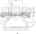
- FIG. 1 is a section view of part of a structure of an electronic device according to an embodiment of the present invention.
- 100-display module 110-first substrate, 120-second substrate, 130-wiring structure, 140-light-emitting portion, 150-light-transmitting cover plate, 160-optical adhesive, 170-polarizer, 180-foam, 200-camera module, 210-camera body, 211-light-entrance hole, 212-bracket, 213-light-sensing chip, 220-light-shielding layer, 221-second light-passing hole.
- an embodiment of the present invention provides an electronic device.
- the electronic device may specifically include a display module 100 and a camera module 200.
- the display module 100 may specifically include a first substrate 110, a second substrate 120 and a wiring structure 130, wherein the first substrate 110 and the second substrate 120 are stacked, and the wiring structure 130 is disposed on a surface of the second substrate 120 facing the first substrate 110.
- the first substrate 110 and the second substrate 120 may be glass plates, and a thin film transistor may be disposed on the second substrate 120.
- the wiring structure 130 may be ring-shaped structure, the wiring structure 130 is provided with a first light-passing hole, and the first light-passing hole enables light to pass through, so that light in the external environment can enter the camera module 200.
- the display module 100 may further include a light-emitting portion 140, a light-transmitting cover plate 150, an optical adhesive 160, a polarizer 170 and foam 180, wherein the light-emitting portion 140 may be disposed between the first substrate 110 and the second substrate 120, and the light-emitting portion 140 may be an organic light-emitting layer; the polarizer 170 may be disposed on a surface of the first substrate 110 facing away from the second substrate 120; the light-transmitting cover plate 150 is located on one side of the first substrate 110 away from the second substrate 120, and the light-transmitting cover plate 150 may be connected to the polarizer 170 through the optical adhesive 160; the foam 180 may be disposed on one side of the second substrate 120 away from the first substrate 110, the foam 180 may adhere to the second substrate 120 and may be provided with an avoidance hole, and at least one part of the camera module 200 may be located in the avoidance hole, so that the influence on the normal work of the camera module 200 by stray light in the display module 100 is avoided
- the camera module 200 may specifically include a camera body 210 and a light-shielding layer 220, wherein the camera body 210 is provided with a light-entrance hole 211, the second substrate 120 is located between the first substrate 110 and the camera body 210, the light-shielding layer 220 is disposed on a surface of the second substrate 120 facing the camera body 210, and the light-shielding layer 220 is provided with a second light-passing hole 221.
- the camera body 210 may specifically include a bracket 212, a lens assembly and a light-sensing chip 213, the lens assembly is disposed on the bracket 212, and the lens assembly may include a convex lens, a concave lens and other lenses, so that the light converging effect can be achieved; and the light-sensing chip 213 may be disposed in the bracket 212, the light-sensing chip 213 is provided with a light-sensing area for sensing light, and the light-sensing chip 213 may convert an optical signal into an electrical signal, so that corresponding image information is acquired.
- the second light-passing hole 221 enables light to pass through, so that light in the external environment can enter the camera module 200 and arrive at the light-sensing area of the light-sensing chip 213, and a shooting function can be realized.
- the wiring structure 130 and the light-shielding layer 220 can play a role in shielding light, and the first light-passing hole, the second light-passing hole 221 and the light-entrance hole 211 are arranged in the optical axis direction of the camera module 200, so light in the external environment can sequentially pass through the first light-passing hole and the second light-passing hole 221, and finally pass through the light-entrance hole 211 to enter the camera module 200, and the camera module 200 can realize the shooting function.
- An orthographic projection of the second light-passing hole 221 on a plane perpendicular to the optical axis direction of the camera module 200 is within an orthographic projection of the light-entrance hole 211 on the plane perpendicular to the optical axis direction, and the orthographic projection of the second light-passing hole 221 on the plane perpendicular to the optical axis direction is within an orthographic projection of the first light-passing hole on the plane perpendicular to the optical axis direction. That is, during observation in the optical axis direction of the camera module 200, an overall size of the first light-passing hole and an overall size of the light-entrance hole 211 are greater than an overall size of the second light-passing hole 221.
- the size of the light-entrance hole 211 is slightly large. Such arrangement does not affect the screen-to-body ratio of the display module 100 and can ensure that light in the external environment enters the camera module 200 as much as possible.
- the second light-passing hole 221 will affect the screen-to-body ratio of the display module 100; therefore, on the premise of meeting the shooting requirement of the camera module 200, the second light-passing hole 221 may be set as small as possible, thereby reducing the occupancy rate of the light-shielding layer 220 on the display area and increasing the screen-to-body ratio of the electronic device.
- the first light-passing hole is located above the second light-passing hole 221; therefore, the first light-passing hole is slightly larger than the second light-passing hole 221, so that more light can enter the second light-passing hole 221 through the first light-passing hole, and the shooting effect of the camera module 200 is ensured better.
- the light-shielding layer 220 of the camera module 200 is disposed on the display module 100.
- a distance between the light-shielding layer 220 and the display module 100 is nearly zero, so the first light-passing hole may be smaller; and on the other hand, there is no assembling error between the display module 100 and the light-shielding layer 220, so it is unnecessary to consider the assembling error when the first light-passing hole is formed, the size of the first light-passing hole may be further reduced, and the screen-to-body ratio of the electronic device is higher. Meanwhile, after the size of the first light-passing hole is reduced, the appearance texture of the electronic device is improved, and the user experience is improved accordingly.
- H A+(B+D) ⁇ 2
- H is the size of a hole on the appearance surface of the display module 100 which cannot be used for displaying
- A is a hole diameter of the second light-passing hole 221
- B is a hole diameter difference value between the first light-passing hole and the second light-passing hole 221
- D is a width of the wiring structure 130.
- A is basically a fixed value; since the light-shielding layer 220 is disposed on the display module 100, a distance Z between the wiring structure 130 and the light-shielding layer 220 is smaller than a distance between the wiring structure 130 and the light-shielding layer 220 in the background art; meanwhile, the field of view ⁇ of the camera module 200 is also a fixed value, so according to the Pythagorean theorem, B is reduced compared with the background art, that is, a hole diameter of the firs light-passing hole may be set smaller.
- a distance S between a hole wall of the first light-passing hole and a hole wall of the second light-passing hole 221 in a direction perpendicular to the optical axis is a product of h and tan ⁇ , wherein h is a thickness of the second substrate 120, and ⁇ is an angle of refraction angle when light passes through the second substrate 120.
- the size of the first light-passing hole may just meet that light needing to enter the camera module 200 can be propagated to the second light-passing hole 221 through the first light-passing hole, which will not reduce the light entering the camera module 200 due to too small first light-passing hole and will not enlarge the hole on the appearance of the display module 100 that cannot be used for displaying due to too large first light-passing hole; therefore, this arrangement mode can meet the shooting requirement of the camera module 200 and also can further increase the screen-to-body ratio of the electronic device.
- the outline shapes of the wiring structure 130 and the light-shielding layer 220 may be disposed flexibly, for example, the outline shapes may be a rectangle, a circle and an ellipse; meanwhile, the shapes of the first light-passing hole and the second light-passing hole may be selected flexibly, for example, the first light-passing hole and the second light-passing hole may be a rectangular hole, a circular hole, an elliptic hole and the like.
- the orthographic projection of the light-entrance hole 211 on the plane perpendicular to the above optical axis direction may be within the orthographic projection of the first light-passing hole on the plane perpendicular to the optical axis direction, or the orthographic projection of the first light-passing hole on the plane perpendicular to the optical axis direction may be within the orthographic projection of the light-entrance hole 211 on the plane perpendicular to the above optical axis direction.
- a distance between a focus of the camera body 210 and the light-shielding layer 220 in the above optical axis direction may be a preset value. That is, when the position of the light-shielding layer 220 changes, the position of the camera body 210 changes accordingly to ensure that the focus of the camera body 210 and the light-shielding layer 220 keep mutually matched positions, so that the shooting effect is improved.
- the distance between the camera body 210 and the display module 100 can be further reduced, and the display module 100 and the camera module 200 are distributed more compact, so that it is more beneficial to stacking of parts in the electronic device.
- the forming manner of the light-shielding layer 220 has various implementation solutions.
- the light-shielding layer 220 may be formed by a film-coating process. That is, the light-shielding layer 220 may be a film-coating structure. This film-coating structure is convenient to form, and the thickness of the formed light-shielding layer 220 is smaller, so that it is more beneficial to control the thickness of the electronic device.
- the shielding layer 220 is disposed on the surface of the second substrate 120 facing the camera body 210, and it is necessary to arrange a thin film transistor and other structures on the surface of the second substrate 120 facing away from the camera body 210 through an evaporation process; therefore, the light-shielding layer 220 may be coated after the evaporation process and the bonding process of the first substrate 110 and the second substrate 120 are performed, or the light-shielding layer 220 may be coated before the evaporation process and the bonding process of the first substrate 110 and the second substrate 120 are performed.
- the light-shielding layer 220 may also be a printing structure. That is, the light-shielding layer 220 may be formed on the surface of the second substrate 120 facing the camera body 210 through a printing process, and this manner has the advantages of convenience in implementation and small thickness of the formed light-shielding layer 220. Specifically, the light-shielding layer 220 may be printed after the evaporation process and the bonding process of the first substrate 110 and the second substrate 120 are performed, or the light-shielding layer 220 may be printed before the evaporation process and the bonding process of the first substrate 110 and the second substrate 120 are performed.
- the alignment and fixation between the light-shielding layer 220 and the camera body 210 can be realized through by means of accurately positioning a charge-coupled device (Charge-coupled Device, CCD) camera and driving the camera module 200 by a micromotor to dynamically adjust alignment, so that the relative position of the light-shielding layer 220 and the camera body 210 has higher precision, the imaging effect of the camera module 200 is ensured, it is unnecessary to consider the alignment error and increase the size of the first light-passing hole, and the screen-to-body ratio of the electronic device can be increased.
- CCD Charge-coupled Device
- the electronic device disclosed in the embodiments of the present invention may be a smart phone, a tablet computer, an e-book reader, or a wearable device.
- the electronic device may also be other devices, which is not limited in the embodiments of the present invention.
Landscapes
- Engineering & Computer Science (AREA)
- Signal Processing (AREA)
- Multimedia (AREA)
- Theoretical Computer Science (AREA)
- Physics & Mathematics (AREA)
- General Physics & Mathematics (AREA)
- Computer Hardware Design (AREA)
- Human Computer Interaction (AREA)
- General Engineering & Computer Science (AREA)
- Studio Devices (AREA)
Claims (7)
- Un dispositif électronique, comprenant :un module unité d'affichage (100), où le module unité d'affichage (100) comprend un premier substrat (110), un deuxième substrat (120) et une structure de câblage (130), le premier substrat (110) et le deuxième substrat (120) sont empilés, la structure de câblage (130) est disposée sur une surface du deuxième substrat (120) faisant face au premier substrat (110), et la structure de câblage (130) est pourvue d'un premier trou laissant passer la lumière ; etun module caméra (200), où le module caméra (200) comprend un corps de caméra (210) et une couche de protection contre la lumière (220), le corps de caméra (210) est pourvu d'un trou d'entrée de lumière (211), le deuxième substrat (120) est placé entre le premier substrat (110) et le corps de caméra (210), caractérisé en ce que la couche de protection contre la lumière (220) est disposée sur une surface du deuxième substrat (120) faisant face au corps de caméra (210), la couche de protection contre la lumière (220) étant pourvue d'un deuxième trou laissant passer la lumière (221) ;le premier trou laissant passer la lumière, le deuxième trou laissant passer la lumière (221) et le trou d'entrée de lumière (211) sont agencés dans une direction d'axe optique du module caméra (200), une projection orthographique du deuxième trou laissant passer la lumière (221) sur un plan perpendiculaire à la direction d'axe optique est à l'intérieur d'une projection orthographique du trou d'entrée de lumière (211) sur le plan perpendiculaire à la direction d'axe optique, et la projection orthographique du deuxième trou laissant passer la lumière (221) sur le plan perpendiculaire à la direction d'axe optique est à l'intérieur d'une projection orthographique du premier trou laissant passer la lumière sur le plan perpendiculaire à la direction d'axe optique.
- Le dispositif électronique selon la revendication 1, où dans une section passant à travers l'axe optique, une distance S entre une paroi de trou du premier trou laissant passer la lumière et une paroi de trou du deuxième trou laissant passer la lumière (221) dans une direction perpendiculaire à l'axe optique est un produit de h et tana, où h est une épaisseur du deuxième substrat (120), et a est un angle de réfraction lorsque de la lumière passe à travers le deuxième substrat (120).
- Le dispositif électronique selon la revendication 1, où la structure de câblage (130) et la couche de protection contre la lumière (220) sont des structures configurées en anneau, et une largeur radiale de la couche de protection contre la lumière (220) est plus petite qu'une largeur radiale de la structure de câblage (130).
- Le dispositif électronique selon la revendication 1, où la projection orthographique du trou d'entrée de lumière (211) sur le plan perpendiculaire à la direction d'axe optique est à l'intérieur de la projection orthographique du premier trou laissant passer la lumière sur le plan perpendiculaire à la direction d'axe optique.
- Le dispositif électronique selon la revendication 1, où une distance entre un foyer du corps de caméra (210) et la couche de protection contre la lumière (220) dans la direction d'axe optique est une valeur prédéfinie.
- Le dispositif électronique selon la revendication 1, où la couche de protection contre la lumière (220) est une structure à enduction pelliculaire.
- Le dispositif électronique selon la revendication 1, où la couche de protection contre la lumière (220) est une structure à impression.
Applications Claiming Priority (2)
| Application Number | Priority Date | Filing Date | Title |
|---|---|---|---|
| CN201911130035.6A CN110728905B (zh) | 2019-11-18 | 2019-11-18 | 电子设备 |
| PCT/CN2020/128942 WO2021098631A1 (fr) | 2019-11-18 | 2020-11-16 | Dispositif électronique |
Publications (3)
| Publication Number | Publication Date |
|---|---|
| EP4064255A1 EP4064255A1 (fr) | 2022-09-28 |
| EP4064255A4 EP4064255A4 (fr) | 2023-01-04 |
| EP4064255B1 true EP4064255B1 (fr) | 2025-03-05 |
Family
ID=69225389
Family Applications (1)
| Application Number | Title | Priority Date | Filing Date |
|---|---|---|---|
| EP20891006.7A Active EP4064255B1 (fr) | 2019-11-18 | 2020-11-16 | Dispositif électronique |
Country Status (5)
| Country | Link |
|---|---|
| US (1) | US12149813B2 (fr) |
| EP (1) | EP4064255B1 (fr) |
| CN (1) | CN110728905B (fr) |
| ES (1) | ES3017421T3 (fr) |
| WO (1) | WO2021098631A1 (fr) |
Families Citing this family (5)
| Publication number | Priority date | Publication date | Assignee | Title |
|---|---|---|---|---|
| CN110769095B (zh) * | 2019-10-16 | 2022-05-20 | Oppo广东移动通信有限公司 | 电子设备的屏幕组件及电子设备 |
| CN110728905B (zh) * | 2019-11-18 | 2021-01-26 | 维沃移动通信有限公司 | 电子设备 |
| CN110730293B (zh) * | 2019-11-18 | 2021-04-06 | 维沃移动通信有限公司 | 电子设备 |
| WO2022093294A1 (fr) * | 2020-10-27 | 2022-05-05 | Google Llc | Système et appareil de caméra sous dispositif d'affichage |
| EP4727145A1 (fr) * | 2024-10-12 | 2026-04-15 | Sharetronic Data Technology Co., Ltd. | Ensemble caméra |
Family Cites Families (17)
| Publication number | Priority date | Publication date | Assignee | Title |
|---|---|---|---|---|
| JP4698874B2 (ja) * | 2001-04-24 | 2011-06-08 | ローム株式会社 | イメージセンサモジュール、およびイメージセンサモジュールの製造方法 |
| JP2005116628A (ja) * | 2003-10-03 | 2005-04-28 | Matsushita Electric Ind Co Ltd | 固体撮像装置およびその製造方法 |
| KR102055204B1 (ko) * | 2013-09-09 | 2019-12-12 | 엘지전자 주식회사 | 카메라 모듈을 포함한 표시장치 |
| TWI577971B (zh) * | 2015-10-22 | 2017-04-11 | 原相科技股份有限公司 | 雙孔徑測距系統 |
| CN108073900B (zh) * | 2017-12-14 | 2021-01-08 | 京东方科技集团股份有限公司 | 用于指纹识别的柔性显示面板、显示装置及指纹识别方法 |
| CN108957829A (zh) * | 2018-07-06 | 2018-12-07 | Oppo广东移动通信有限公司 | 显示屏组件、电子设备及电子设备的制作方法 |
| CN108900672B (zh) * | 2018-07-06 | 2021-05-04 | Oppo广东移动通信有限公司 | 电子设备及电子设备的制作方法 |
| US11366348B2 (en) * | 2018-08-27 | 2022-06-21 | Lg Display Co., Ltd. | Display device |
| CN209233928U (zh) * | 2019-01-04 | 2019-08-09 | Oppo广东移动通信有限公司 | 电子设备 |
| CN110034151A (zh) * | 2019-03-29 | 2019-07-19 | 武汉华星光电半导体显示技术有限公司 | 显示面板及显示装置 |
| CN110299072A (zh) * | 2019-06-28 | 2019-10-01 | Oppo广东移动通信有限公司 | 电子设备 |
| CN110426878A (zh) * | 2019-07-16 | 2019-11-08 | 武汉华星光电技术有限公司 | 显示装置 |
| JP2021028690A (ja) * | 2019-08-09 | 2021-02-25 | 株式会社ジャパンディスプレイ | 電子機器 |
| CN110827672B (zh) * | 2019-11-18 | 2021-09-21 | 维沃移动通信有限公司 | 电子设备 |
| CN110728905B (zh) * | 2019-11-18 | 2021-01-26 | 维沃移动通信有限公司 | 电子设备 |
| CN110784636B (zh) * | 2019-11-18 | 2021-03-05 | 维沃移动通信有限公司 | 电子设备 |
| CN110784635B (zh) * | 2019-11-18 | 2021-05-18 | 维沃移动通信有限公司 | 电子设备 |
-
2019
- 2019-11-18 CN CN201911130035.6A patent/CN110728905B/zh active Active
-
2020
- 2020-11-16 ES ES20891006T patent/ES3017421T3/es active Active
- 2020-11-16 EP EP20891006.7A patent/EP4064255B1/fr active Active
- 2020-11-16 WO PCT/CN2020/128942 patent/WO2021098631A1/fr not_active Ceased
-
2022
- 2022-05-17 US US17/746,902 patent/US12149813B2/en active Active
Also Published As
| Publication number | Publication date |
|---|---|
| CN110728905A (zh) | 2020-01-24 |
| WO2021098631A1 (fr) | 2021-05-27 |
| ES3017421T3 (en) | 2025-05-12 |
| CN110728905B (zh) | 2021-01-26 |
| US12149813B2 (en) | 2024-11-19 |
| EP4064255A1 (fr) | 2022-09-28 |
| US20220279104A1 (en) | 2022-09-01 |
| EP4064255A4 (fr) | 2023-01-04 |
Similar Documents
| Publication | Publication Date | Title |
|---|---|---|
| EP4064255B1 (fr) | Dispositif électronique | |
| EP4064676B1 (fr) | Dispositif électronique | |
| US12069360B2 (en) | Electronic device | |
| EP4064254B1 (fr) | Dispositif électronique | |
| CN209895353U (zh) | 指纹识别装置和电子设备 | |
| TWI623787B (zh) | 含有塑膠透鏡的成像透鏡組、成像鏡頭模組及電子裝置 | |
| CN110730293B (zh) | 电子设备 | |
| TWI657281B (zh) | 含有塑膠透鏡的成像透鏡組、成像鏡頭模組及電子裝置 | |
| JP2017090875A (ja) | レンズモジュール | |
| WO2019237876A1 (fr) | Module de caméra et dispositif électronique | |
| CN110166679B (zh) | 电子设备 | |
| CN208128305U (zh) | 摄像头模组及电子设备 | |
| WO2021036703A1 (fr) | Appareil d'empreintes digitales, dispositif électronique et procédé de fabrication associé | |
| EP4598038A1 (fr) | Ensemble lentille et dispositif électronique le comprenant | |
| CN209964149U (zh) | 电子设备 | |
| CN210429124U (zh) | 电子设备 | |
| CN210327670U (zh) | 电子设备 | |
| WO2022228440A1 (fr) | Module de lentille et dispositif électronique | |
| KR20240048442A (ko) | 렌즈 어셈블리 및 그를 포함하는 전자 장치 | |
| WO2022141606A1 (fr) | Appareil de détection optique d'empreintes digitales et dispositif électronique |
Legal Events
| Date | Code | Title | Description |
|---|---|---|---|
| STAA | Information on the status of an ep patent application or granted ep patent |
Free format text: STATUS: THE INTERNATIONAL PUBLICATION HAS BEEN MADE |
|
| PUAI | Public reference made under article 153(3) epc to a published international application that has entered the european phase |
Free format text: ORIGINAL CODE: 0009012 |
|
| STAA | Information on the status of an ep patent application or granted ep patent |
Free format text: STATUS: REQUEST FOR EXAMINATION WAS MADE |
|
| 17P | Request for examination filed |
Effective date: 20220609 |
|
| AK | Designated contracting states |
Kind code of ref document: A1 Designated state(s): AL AT BE BG CH CY CZ DE DK EE ES FI FR GB GR HR HU IE IS IT LI LT LU LV MC MK MT NL NO PL PT RO RS SE SI SK SM TR |
|
| REG | Reference to a national code |
Ref country code: DE Ref legal event code: R079 Free format text: PREVIOUS MAIN CLASS: G09F0009000000 Ipc: H04M0001020000 Ref country code: DE Ref legal event code: R079 Ref document number: 602020047422 Country of ref document: DE Free format text: PREVIOUS MAIN CLASS: G09F0009000000 Ipc: H04M0001020000 |
|
| A4 | Supplementary search report drawn up and despatched |
Effective date: 20221202 |
|
| RIC1 | Information provided on ipc code assigned before grant |
Ipc: G06F 1/16 20060101ALI20221128BHEP Ipc: H04N 5/225 20060101ALI20221128BHEP Ipc: H04M 1/02 20060101AFI20221128BHEP |
|
| DAV | Request for validation of the european patent (deleted) | ||
| DAX | Request for extension of the european patent (deleted) | ||
| GRAP | Despatch of communication of intention to grant a patent |
Free format text: ORIGINAL CODE: EPIDOSNIGR1 |
|
| STAA | Information on the status of an ep patent application or granted ep patent |
Free format text: STATUS: GRANT OF PATENT IS INTENDED |
|
| RIC1 | Information provided on ipc code assigned before grant |
Ipc: H04N 23/55 20230101ALI20241112BHEP Ipc: G06F 1/16 20060101ALI20241112BHEP Ipc: H04M 1/02 20060101AFI20241112BHEP |
|
| INTG | Intention to grant announced |
Effective date: 20241205 |
|
| GRAS | Grant fee paid |
Free format text: ORIGINAL CODE: EPIDOSNIGR3 |
|
| GRAA | (expected) grant |
Free format text: ORIGINAL CODE: 0009210 |
|
| STAA | Information on the status of an ep patent application or granted ep patent |
Free format text: STATUS: THE PATENT HAS BEEN GRANTED |
|
| AK | Designated contracting states |
Kind code of ref document: B1 Designated state(s): AL AT BE BG CH CY CZ DE DK EE ES FI FR GB GR HR HU IE IS IT LI LT LU LV MC MK MT NL NO PL PT RO RS SE SI SK SM TR |
|
| REG | Reference to a national code |
Ref country code: GB Ref legal event code: FG4D |
|
| REG | Reference to a national code |
Ref country code: CH Ref legal event code: EP |
|
| REG | Reference to a national code |
Ref country code: DE Ref legal event code: R096 Ref document number: 602020047422 Country of ref document: DE |
|
| REG | Reference to a national code |
Ref country code: IE Ref legal event code: FG4D |
|
| REG | Reference to a national code |
Ref country code: NL Ref legal event code: FP |
|
| REG | Reference to a national code |
Ref country code: ES Ref legal event code: FG2A Ref document number: 3017421 Country of ref document: ES Kind code of ref document: T3 Effective date: 20250512 |
|
| PG25 | Lapsed in a contracting state [announced via postgrant information from national office to epo] |
Ref country code: RS Free format text: LAPSE BECAUSE OF FAILURE TO SUBMIT A TRANSLATION OF THE DESCRIPTION OR TO PAY THE FEE WITHIN THE PRESCRIBED TIME-LIMIT Effective date: 20250605 |
|
| PG25 | Lapsed in a contracting state [announced via postgrant information from national office to epo] |
Ref country code: FI Free format text: LAPSE BECAUSE OF FAILURE TO SUBMIT A TRANSLATION OF THE DESCRIPTION OR TO PAY THE FEE WITHIN THE PRESCRIBED TIME-LIMIT Effective date: 20250305 |
|
| REG | Reference to a national code |
Ref country code: LT Ref legal event code: MG9D |
|
| PG25 | Lapsed in a contracting state [announced via postgrant information from national office to epo] |
Ref country code: NO Free format text: LAPSE BECAUSE OF FAILURE TO SUBMIT A TRANSLATION OF THE DESCRIPTION OR TO PAY THE FEE WITHIN THE PRESCRIBED TIME-LIMIT Effective date: 20250605 |
|
| PG25 | Lapsed in a contracting state [announced via postgrant information from national office to epo] |
Ref country code: HR Free format text: LAPSE BECAUSE OF FAILURE TO SUBMIT A TRANSLATION OF THE DESCRIPTION OR TO PAY THE FEE WITHIN THE PRESCRIBED TIME-LIMIT Effective date: 20250305 |
|
| PG25 | Lapsed in a contracting state [announced via postgrant information from national office to epo] |
Ref country code: LV Free format text: LAPSE BECAUSE OF FAILURE TO SUBMIT A TRANSLATION OF THE DESCRIPTION OR TO PAY THE FEE WITHIN THE PRESCRIBED TIME-LIMIT Effective date: 20250305 |
|
| PG25 | Lapsed in a contracting state [announced via postgrant information from national office to epo] |
Ref country code: GR Free format text: LAPSE BECAUSE OF FAILURE TO SUBMIT A TRANSLATION OF THE DESCRIPTION OR TO PAY THE FEE WITHIN THE PRESCRIBED TIME-LIMIT Effective date: 20250606 Ref country code: BG Free format text: LAPSE BECAUSE OF FAILURE TO SUBMIT A TRANSLATION OF THE DESCRIPTION OR TO PAY THE FEE WITHIN THE PRESCRIBED TIME-LIMIT Effective date: 20250305 |
|
| REG | Reference to a national code |
Ref country code: AT Ref legal event code: MK05 Ref document number: 1774006 Country of ref document: AT Kind code of ref document: T Effective date: 20250305 |
|
| PG25 | Lapsed in a contracting state [announced via postgrant information from national office to epo] |
Ref country code: SE Free format text: LAPSE BECAUSE OF FAILURE TO SUBMIT A TRANSLATION OF THE DESCRIPTION OR TO PAY THE FEE WITHIN THE PRESCRIBED TIME-LIMIT Effective date: 20250305 |
|
| PG25 | Lapsed in a contracting state [announced via postgrant information from national office to epo] |
Ref country code: SM Free format text: LAPSE BECAUSE OF FAILURE TO SUBMIT A TRANSLATION OF THE DESCRIPTION OR TO PAY THE FEE WITHIN THE PRESCRIBED TIME-LIMIT Effective date: 20250305 |
|
| PG25 | Lapsed in a contracting state [announced via postgrant information from national office to epo] |
Ref country code: PT Free format text: LAPSE BECAUSE OF FAILURE TO SUBMIT A TRANSLATION OF THE DESCRIPTION OR TO PAY THE FEE WITHIN THE PRESCRIBED TIME-LIMIT Effective date: 20250707 |
|
| PG25 | Lapsed in a contracting state [announced via postgrant information from national office to epo] |
Ref country code: PL Free format text: LAPSE BECAUSE OF FAILURE TO SUBMIT A TRANSLATION OF THE DESCRIPTION OR TO PAY THE FEE WITHIN THE PRESCRIBED TIME-LIMIT Effective date: 20250305 |
|
| PG25 | Lapsed in a contracting state [announced via postgrant information from national office to epo] |
Ref country code: AT Free format text: LAPSE BECAUSE OF FAILURE TO SUBMIT A TRANSLATION OF THE DESCRIPTION OR TO PAY THE FEE WITHIN THE PRESCRIBED TIME-LIMIT Effective date: 20250305 |
|
| PGFP | Annual fee paid to national office [announced via postgrant information from national office to epo] |
Ref country code: FR Payment date: 20250930 Year of fee payment: 6 |
|
| PG25 | Lapsed in a contracting state [announced via postgrant information from national office to epo] |
Ref country code: CZ Free format text: LAPSE BECAUSE OF FAILURE TO SUBMIT A TRANSLATION OF THE DESCRIPTION OR TO PAY THE FEE WITHIN THE PRESCRIBED TIME-LIMIT Effective date: 20250305 Ref country code: EE Free format text: LAPSE BECAUSE OF FAILURE TO SUBMIT A TRANSLATION OF THE DESCRIPTION OR TO PAY THE FEE WITHIN THE PRESCRIBED TIME-LIMIT Effective date: 20250305 |
|
| PG25 | Lapsed in a contracting state [announced via postgrant information from national office to epo] |
Ref country code: RO Free format text: LAPSE BECAUSE OF FAILURE TO SUBMIT A TRANSLATION OF THE DESCRIPTION OR TO PAY THE FEE WITHIN THE PRESCRIBED TIME-LIMIT Effective date: 20250305 |
|
| PG25 | Lapsed in a contracting state [announced via postgrant information from national office to epo] |
Ref country code: SK Free format text: LAPSE BECAUSE OF FAILURE TO SUBMIT A TRANSLATION OF THE DESCRIPTION OR TO PAY THE FEE WITHIN THE PRESCRIBED TIME-LIMIT Effective date: 20250305 |
|
| PG25 | Lapsed in a contracting state [announced via postgrant information from national office to epo] |
Ref country code: IS Free format text: LAPSE BECAUSE OF FAILURE TO SUBMIT A TRANSLATION OF THE DESCRIPTION OR TO PAY THE FEE WITHIN THE PRESCRIBED TIME-LIMIT Effective date: 20250705 |
|
| PGFP | Annual fee paid to national office [announced via postgrant information from national office to epo] |
Ref country code: NL Payment date: 20251003 Year of fee payment: 6 |
|
| REG | Reference to a national code |
Ref country code: DE Ref legal event code: R097 Ref document number: 602020047422 Country of ref document: DE |
|
| PGFP | Annual fee paid to national office [announced via postgrant information from national office to epo] |
Ref country code: DE Payment date: 20250930 Year of fee payment: 6 |
|
| PGFP | Annual fee paid to national office [announced via postgrant information from national office to epo] |
Ref country code: GB Payment date: 20251001 Year of fee payment: 6 |
|
| PLBE | No opposition filed within time limit |
Free format text: ORIGINAL CODE: 0009261 |
|
| STAA | Information on the status of an ep patent application or granted ep patent |
Free format text: STATUS: NO OPPOSITION FILED WITHIN TIME LIMIT |
|
| PG25 | Lapsed in a contracting state [announced via postgrant information from national office to epo] |
Ref country code: DK Free format text: LAPSE BECAUSE OF FAILURE TO SUBMIT A TRANSLATION OF THE DESCRIPTION OR TO PAY THE FEE WITHIN THE PRESCRIBED TIME-LIMIT Effective date: 20250305 |
|
| PGFP | Annual fee paid to national office [announced via postgrant information from national office to epo] |
Ref country code: IT Payment date: 20251022 Year of fee payment: 6 |
|
| REG | Reference to a national code |
Ref country code: CH Ref legal event code: L10 Free format text: ST27 STATUS EVENT CODE: U-0-0-L10-L00 (AS PROVIDED BY THE NATIONAL OFFICE) Effective date: 20260114 |
|
| PGFP | Annual fee paid to national office [announced via postgrant information from national office to epo] |
Ref country code: ES Payment date: 20251211 Year of fee payment: 6 |
|
| 26N | No opposition filed |
Effective date: 20251208 |