EP4057308B1 - Mehrfachwicklungsspule und stromversorgungsmodul - Google Patents
Mehrfachwicklungsspule und stromversorgungsmodul Download PDFInfo
- Publication number
- EP4057308B1 EP4057308B1 EP22159645.5A EP22159645A EP4057308B1 EP 4057308 B1 EP4057308 B1 EP 4057308B1 EP 22159645 A EP22159645 A EP 22159645A EP 4057308 B1 EP4057308 B1 EP 4057308B1
- Authority
- EP
- European Patent Office
- Prior art keywords
- magnetic
- winding
- magnetic column
- cover plate
- column
- Prior art date
- Legal status (The legal status is an assumption and is not a legal conclusion. Google has not performed a legal analysis and makes no representation as to the accuracy of the status listed.)
- Active
Links
Images


Classifications
-
- H—ELECTRICITY
- H01—ELECTRIC ELEMENTS
- H01F—MAGNETS; INDUCTANCES; TRANSFORMERS; SELECTION OF MATERIALS FOR THEIR MAGNETIC PROPERTIES
- H01F37/00—Fixed inductances not covered by group H01F17/00
-
- H—ELECTRICITY
- H01—ELECTRIC ELEMENTS
- H01F—MAGNETS; INDUCTANCES; TRANSFORMERS; SELECTION OF MATERIALS FOR THEIR MAGNETIC PROPERTIES
- H01F27/00—Details of transformers or inductances, in general
- H01F27/08—Cooling; Ventilating
-
- H—ELECTRICITY
- H01—ELECTRIC ELEMENTS
- H01F—MAGNETS; INDUCTANCES; TRANSFORMERS; SELECTION OF MATERIALS FOR THEIR MAGNETIC PROPERTIES
- H01F27/00—Details of transformers or inductances, in general
- H01F27/02—Casings
-
- H—ELECTRICITY
- H01—ELECTRIC ELEMENTS
- H01F—MAGNETS; INDUCTANCES; TRANSFORMERS; SELECTION OF MATERIALS FOR THEIR MAGNETIC PROPERTIES
- H01F27/00—Details of transformers or inductances, in general
- H01F27/24—Magnetic cores
-
- H—ELECTRICITY
- H01—ELECTRIC ELEMENTS
- H01F—MAGNETS; INDUCTANCES; TRANSFORMERS; SELECTION OF MATERIALS FOR THEIR MAGNETIC PROPERTIES
- H01F27/00—Details of transformers or inductances, in general
- H01F27/24—Magnetic cores
- H01F27/26—Fastening parts of the core together; Fastening or mounting the core on casing or support
- H01F27/263—Fastening parts of the core together
-
- H—ELECTRICITY
- H01—ELECTRIC ELEMENTS
- H01F—MAGNETS; INDUCTANCES; TRANSFORMERS; SELECTION OF MATERIALS FOR THEIR MAGNETIC PROPERTIES
- H01F27/00—Details of transformers or inductances, in general
- H01F27/28—Coils; Windings; Conductive connections
-
- H—ELECTRICITY
- H01—ELECTRIC ELEMENTS
- H01F—MAGNETS; INDUCTANCES; TRANSFORMERS; SELECTION OF MATERIALS FOR THEIR MAGNETIC PROPERTIES
- H01F27/00—Details of transformers or inductances, in general
- H01F27/28—Coils; Windings; Conductive connections
- H01F27/2823—Wires
-
- H—ELECTRICITY
- H01—ELECTRIC ELEMENTS
- H01F—MAGNETS; INDUCTANCES; TRANSFORMERS; SELECTION OF MATERIALS FOR THEIR MAGNETIC PROPERTIES
- H01F27/00—Details of transformers or inductances, in general
- H01F27/28—Coils; Windings; Conductive connections
- H01F27/2847—Sheets; Strips
-
- H—ELECTRICITY
- H01—ELECTRIC ELEMENTS
- H01F—MAGNETS; INDUCTANCES; TRANSFORMERS; SELECTION OF MATERIALS FOR THEIR MAGNETIC PROPERTIES
- H01F27/00—Details of transformers or inductances, in general
- H01F27/28—Coils; Windings; Conductive connections
- H01F27/30—Fastening or clamping coils, windings, or parts thereof together; Fastening or mounting coils or windings on core, casing, or other support
- H01F27/306—Fastening or mounting coils or windings on core, casing or other support
-
- H—ELECTRICITY
- H01—ELECTRIC ELEMENTS
- H01F—MAGNETS; INDUCTANCES; TRANSFORMERS; SELECTION OF MATERIALS FOR THEIR MAGNETIC PROPERTIES
- H01F3/00—Cores, Yokes, or armatures
- H01F3/10—Composite arrangements of magnetic circuits
- H01F3/14—Constrictions; Gaps, e.g. air-gaps
-
- H—ELECTRICITY
- H02—GENERATION; CONVERSION OR DISTRIBUTION OF ELECTRIC POWER
- H02M—APPARATUS FOR CONVERSION BETWEEN AC AND AC, BETWEEN AC AND DC, OR BETWEEN DC AND DC, AND FOR USE WITH MAINS OR SIMILAR POWER SUPPLY SYSTEMS; CONVERSION OF DC OR AC INPUT POWER INTO SURGE OUTPUT POWER; CONTROL OR REGULATION THEREOF
- H02M3/00—Conversion of DC power input into DC power output
- H02M3/003—Constructional details, e.g. physical layout, assembly, wiring or busbar connections
-
- H—ELECTRICITY
- H01—ELECTRIC ELEMENTS
- H01F—MAGNETS; INDUCTANCES; TRANSFORMERS; SELECTION OF MATERIALS FOR THEIR MAGNETIC PROPERTIES
- H01F3/00—Cores, Yokes, or armatures
- H01F3/10—Composite arrangements of magnetic circuits
- H01F2003/106—Magnetic circuits using combinations of different magnetic materials
-
- H—ELECTRICITY
- H01—ELECTRIC ELEMENTS
- H01F—MAGNETS; INDUCTANCES; TRANSFORMERS; SELECTION OF MATERIALS FOR THEIR MAGNETIC PROPERTIES
- H01F17/00—Fixed inductances of the signal type
- H01F17/04—Fixed inductances of the signal type with magnetic core
- H01F2017/048—Fixed inductances of the signal type with magnetic core with encapsulating core, e.g. made of resin and magnetic powder
-
- H—ELECTRICITY
- H02—GENERATION; CONVERSION OR DISTRIBUTION OF ELECTRIC POWER
- H02M—APPARATUS FOR CONVERSION BETWEEN AC AND AC, BETWEEN AC AND DC, OR BETWEEN DC AND DC, AND FOR USE WITH MAINS OR SIMILAR POWER SUPPLY SYSTEMS; CONVERSION OF DC OR AC INPUT POWER INTO SURGE OUTPUT POWER; CONTROL OR REGULATION THEREOF
- H02M1/00—Details of apparatus for conversion
- H02M1/0064—Magnetic structures combining different functions, e.g. storage, filtering or transformation
-
- H—ELECTRICITY
- H02—GENERATION; CONVERSION OR DISTRIBUTION OF ELECTRIC POWER
- H02M—APPARATUS FOR CONVERSION BETWEEN AC AND AC, BETWEEN AC AND DC, OR BETWEEN DC AND DC, AND FOR USE WITH MAINS OR SIMILAR POWER SUPPLY SYSTEMS; CONVERSION OF DC OR AC INPUT POWER INTO SURGE OUTPUT POWER; CONTROL OR REGULATION THEREOF
- H02M3/00—Conversion of DC power input into DC power output
- H02M3/02—Conversion of DC power input into DC power output without intermediate conversion into AC
- H02M3/04—Conversion of DC power input into DC power output without intermediate conversion into AC by static converters
- H02M3/10—Conversion of DC power input into DC power output without intermediate conversion into AC by static converters using discharge tubes with control electrode or semiconductor devices with control electrode
- H02M3/145—Conversion of DC power input into DC power output without intermediate conversion into AC by static converters using discharge tubes with control electrode or semiconductor devices with control electrode using devices of a triode or transistor type requiring continuous application of a control signal
- H02M3/155—Conversion of DC power input into DC power output without intermediate conversion into AC by static converters using discharge tubes with control electrode or semiconductor devices with control electrode using devices of a triode or transistor type requiring continuous application of a control signal using semiconductor devices only
- H02M3/156—Conversion of DC power input into DC power output without intermediate conversion into AC by static converters using discharge tubes with control electrode or semiconductor devices with control electrode using devices of a triode or transistor type requiring continuous application of a control signal using semiconductor devices only with automatic control of output voltage or current, e.g. switching regulators
- H02M3/158—Conversion of DC power input into DC power output without intermediate conversion into AC by static converters using discharge tubes with control electrode or semiconductor devices with control electrode using devices of a triode or transistor type requiring continuous application of a control signal using semiconductor devices only with automatic control of output voltage or current, e.g. switching regulators including plural semiconductor devices as final control devices for a single load
- H02M3/1584—Conversion of DC power input into DC power output without intermediate conversion into AC by static converters using discharge tubes with control electrode or semiconductor devices with control electrode using devices of a triode or transistor type requiring continuous application of a control signal using semiconductor devices only with automatic control of output voltage or current, e.g. switching regulators including plural semiconductor devices as final control devices for a single load with a plurality of power processing stages connected in parallel
- H02M3/1586—Conversion of DC power input into DC power output without intermediate conversion into AC by static converters using discharge tubes with control electrode or semiconductor devices with control electrode using devices of a triode or transistor type requiring continuous application of a control signal using semiconductor devices only with automatic control of output voltage or current, e.g. switching regulators including plural semiconductor devices as final control devices for a single load with a plurality of power processing stages connected in parallel switched with a phase shift, i.e. interleaved
Definitions
- This disclosure relates to a power supply module and a multi-winding inductor.
- VRM voltage regulation module
- a volume of multi-winding inductor usually has the highest proportion, and an inductance amount of multi-winding inductor is also a main factor that directly affects efficiency and dynamic performance of the whole VRM.
- an inductance amount of multi-winding inductor is also a main factor that directly affects efficiency and dynamic performance of the whole VRM.
- FIG. 1 is the schematic structural view of a VRM as disclosed in Chinese patent application CN107046366A .
- a switching unit 21 as heat source is arranged over the multi-winding inductor 10.
- a coil 13 of the winding inductor coil 13 has one end arranged on an upper surface of the multi-winding inductor 10 and connected to the switching unit 21, and the other end arranged on a lower surface of the multi-winding inductor 10, for connecting to a load.
- Such arrangement is provided such that the switching unit 21 including the heat source is directly connected to a heat sink (not shown) above, thereby maximizing the heat dissipation capability of the VRM.
- the inductor can meet the requirements of leading out PIN on upper and lower sides at the same time, the inductor cannot achieve negative coupling.
- the negative coupling inductor technology can provide a small dynamic sensitivity to meet the high dynamic performance, and the negative coupling inductor can provide a large steady-state sensitivity to achieve high efficiency. Therefore, where the inductor realizes the negative coupling on the basis of leading out the PIN on the upper and lower sides is a hot and difficult problem in the field of VRM.
- US Patent Number US8975995B1 which discloses a coupled inductor includes a ladder magnetic core, a first common leakage plate formed of a magnetic material, and N windings, where N is an integer greater than one.
- the ladder magnetic core includes first and second rails and N rungs, where each of the N rungs connects the first and second rails.
- Each of the N windings includes a respective first portion.
- Each of the N windings is wound around a respective one of the N rungs, and at least two of the N windings are wrapped at least partially around the first common leakage plate such that a first portion of the winding is disposed between an outer surface of the first rail and an outer surface of the first common leakage plate.
- Chinese Patent Application Publication Number CN111899962A which discloses a magnetic integration system of a GaN-based DC-DC converter.
- Each of the first planar inductor coil and the second planar inductor coil has a structure in the shape of the Chinese character ' '.
- the central portion of the first planar inductor coil passes through the space between the first planar magnetic column and the fourth planar magnetic column and the space between the second planar magnetic column and the third planar magnetic column.
- the second planar magnetic column is positioned at an opening position on one side of the first planar inductor coil.
- the fourth planar magnetic column is positioned at an opening position on the other side of the second planar inductor coil.
- the central portion of the second planar inductor coil passes through the space between the first planar magnetic column and the second planar magnetic column and the space between the third planar magnetic column and the fourth planar magnetic column.
- the third planar magnetic column is placed at the opening position on one side of the second planar inductor coil, and the first planar magnetic column is placed at the opening position on the other side of the second planar inductor coil.
- the system can perform decoupling integration through the discrete inductor so as to increase the power density of the converter.
- US Patent Number US9263177B1 which discloses a magnetic device includes a magnetic core and N windings wound at least partially around respective portions of the magnetic core. Each of the N windings has opposing first and second ends. Each first end forms a first connector, and each second end forms a second connector. Each first connector is adapted for coupling to a first substrate in a first plane, and each second connector is adapted for coupling to a second substrate in a second plane, where the second plane is different from the first plane. N is an integer greater than zero.
- An electrical assembly includes a substrate and a power supply module including a magnetic device. The magnetic device at least partially electrically couples the power supply module to the substrate.
- An object of this disclosure is to provide a multi-winding inductor and a power supply module, which not only has a good heat dissipation effect but also facilitate improving efficiency.
- a multi-winding inductor includes a magnetic core and a winding assembly.
- the magnetic core includes a first cover plate, a second plate and four magnetic columns, the first cover plate and the second cover plate being arranged oppositely, the four magnetic columns including a first magnetic column, a second magnetic column, a third magnetic column and a fourth magnetic column orderly arranged counterclockwise, and two ends of each of the four magnetic columns are respectively connected to the first cover plate and the second cover plate.
- the winding assembly includes at least a first winding and a second winding, each of the first winding and the second winding includes a first portion, a second portion and a third portion.
- first portion and the third portion of are connected through the second portion in each of the first winding and the second winding.
- the first portion of the first winding is arranged between the first magnetic column and the second magnetic column.
- the third portion of the first winding is arranged between the third magnetic column and the fourth magnetic column; the first portion of the second winding is arranged between the fourth magnetic column and the first magnetic column; the third portion of the second winding is arranged between the second magnetic column and the third magnetic column.
- the first portion of the first winding extends to a first surface of the magnetic core and forms a first pin of the inductor on the first surface of the magnetic core; the first portion of the second winding extends to the first surface of the magnetic core and forms a third pin of the inductor on the first surface of the magnetic core.
- each of the first winding and the second winding is a flat wire with a width and a thickness, the thickness is less than the width.
- a width direction is parallel to an extension direction of the first magnetic column.
- first winding and the second winding are crosswise such that the second portion of the first winding and the second portion of the second winding are overlapped.
- the first winding is provided with a notch or a hole
- the second winding is provided with a notch or a hole
- the first winding and the second winding are crosswise through the notch or the hole.
- the third portion of the first winding extends to a second surface of the magnetic core so as to form a second pin of an inductor; and the third portion of the second winding extends to a second surface of the magnetic core so as to form a fourth pin of an inductor.
- the first magnetic column, the first cover plate, the third magnetic column and the second cover plate form a first magnetic path; the first cover plate, the second magnetic column, the second cover plate and the fourth magnetic column form a second magnetic path; and a total reluctance of the first magnetic path is less than or greater than or equal to a total reluctance of the second magnetic path.
- the first magnetic column, the first cover plate, the third magnetic column and the second cover plate form a first magnetic path
- the first cover plate, the second magnetic column, the second cover plate and the fourth magnetic column form a second magnetic path
- a total reluctance of the first magnetic path is greater than a total reluctance of the second magnetic path.
- the first magnetic column, the first cover plate, the third magnetic column and the second cover plate form a first magnetic path
- the first cover plate, the second magnetic column, the second cover plate and the fourth magnetic column form a second magnetic path
- a total reluctance of the first magnetic path is equal to a total reluctance of the second magnetic path.
- the total length of air gaps in the first magnetic path is less than the total length of air gaps in the second magnetic path.
- each of first magnetic column, the second magnetic column, the third magnetic column and the fourth magnetic column includes a first portion and a second portion.
- the magnetic core includes a first assembly and a second assembly.
- the first assembly incudes the first cover plate, the first portion of the first magnetic column, the first portion of the second magnetic column, the first portion of the third magnetic column and the first portion of the fourth magnetic column;
- the second assembly comprises the second cover plate, the second portion of the first magnetic column, the second portion of the second magnetic column, the second portion of the third magnetic column and the second portion of the fourth magnetic column.
- Air gap is arranged between the first portion and the second portion of each of first magnetic column, the second magnetic column, the third magnetic column and the fourth magnetic column.
- the magnetic core comprises a first assembly and a second assembly.
- the first assembly includes the first magnetic column, the second magnetic column, the third magnetic column, the fourth magnetic column and one of the first cover plate and the second cover plate
- the second assembly comprises the other one of the first cover plate and the second cover plate, and the air gaps are formed between the first assembly and the second assembly.
- the second magnetic column and the fourth magnetic column are arranged on opposite sides of the first cover plate and the second cover plate, and the air gaps of the second magnetic column are formed between the second magnetic column and the first cover plate and the second cover plate, the air gaps of the fourth magnetic column are formed between the fourth magnetic column and the first cover plate and the second cover plate.
- the magnetic core comprises two U type assemblies and two I type assemblies.
- the U type assembly is made of a ferrite material with high magnetic permeability; and the I type assembly is made of a powder magnetic material with low magnetic permeability.
- the magnetic permeability of at least part of the magnetic material in the second magnetic column and the fourth magnetic column is lower than the magnetic permeability of the magnetic material in the first magnetic column and the third magnetic column.
- the magnetic core is formed by magnetic powder material with an insulation coating, and the magnetic core and the winding are pressed together through a mold to form the multi-winding inductor.
- the magnetic core is formed of a magnetic material, and a ratio of an equivalent magnetic path length to an equivalent section of the first magnetic path is less than a ratio of an equivalent magnetic path length to an equivalent section of the second magnetic path.
- a power supply module includes the multi-winding inductor of this disclosure; and an integrated power module stacked on a first surface of the multi-winding inductor and including at least a first switching unit and a second switching unit.
- the first switching unit is electrically connected with the first pin of the multi-winding inductor
- the second switching unit is electrically connected with the third pin of the multi-winding inductor.
- the first switching unit and the second switching unit have a rectangular shape, a length direction of the first switching unit and a length direction of the second switching unit are in consistent with a width direction of the first winding and a width direction of the second winding, and the width direction of the first winding and the width direction of the second winding are parallel to an extension direction of the magnetic column.
- the power supply module further comprises a plurality of conductive elements arranged around the magnetic core, each of the conductive elements includes a first end and a second end, the first end forms a fifth pin on the first surface of the magnetic core, and the second end forms a sixth pin on the second surface of the magnetic core.
- the plurality of conductive elements includes at least two groups of power connection assemblies that are respectively arranged on a first side and a second side of the multi-winding inductor, wherein the first side and the second side are arranged oppositely; and a signal connection assembly arranged on a third side and/or a fourth side of the multi-winding inductor.
- each group of the power connection assemblies contains an input conductive element and a ground conductive element; each of the input conductive element and the ground conductive element includes a first portion, a second portion and a third portion orderly connected; wherein the second portion is arranged on a side of the multi-winding inductor, and the first portion and the third portion extend to the first surface and the second surface of the multi-winding inductor, respectively.
- the input conductive element and the ground conductive element of each group of the power connection assemblies are arranged side by side.
- the input conductive element and the ground conductive element each include at least one first portion and at least one third portion; the first portions of the input conductive element and the ground conductive element of each group of the power connection assemblies are staggered; the third portions of the input conductive element and the ground conductive element of each group of the power connection assemblies are staggered; and the second portions of the input conductive element and the ground conductive element of each group of the power connection assemblies are overlapped.
- the signal connection assembly comprises a plurality of signal conductive elements arranged side by side.
- each group of the power connection assemblies comprises at least two input conductive elements and at least two ground conductive elements.
- Each of the input conductive elements and the ground conductive elements includes at least two first portions, one second portion and at least two third portions, and the at least two first portions and the at least two third portions are respectively extending from two ends of the second portion.
- the second portions of the at least two input conductive elements and the second portions of the at least two ground conductive elements are alternately overlapped on the side of the multi-winding inductor, the first portions respectively extend to the first surface of the multi-winding inductor, and the third portions respectively extend to the second surface of the multi-winding inductor.
- the at least two first portions of the input conductive element and at least two first portions of the ground conductive element adjacent thereto are staggered; and the at least two third portions of the input conductive element and at least two third portions of the ground conductive element adjacent thereto are staggered.
- the power supply module further includes a bendable substrate, on which the plurality of conductive elements is arranged.
- the bendable substrate comprises a bottom plate, a first side plate, a second side plate and a third side plate, and, the first side plate, the second side plate and the third side plate are formed by bending and extending the bottom plate, wherein the first side plate and the second side plate are arranged oppositely; wherein the plurality of conductive elements comprises a signal connection assembly and at least two groups of power connection assemblies, the at least two groups of power connection assemblies are respectively arranged on the first side plate and the second side plate, and the signal connection assembly is arranged on the third side plate.
- the power supply module further comprises an output capacitor arranged on the bottom plate and located between the second surface of the magnetic core and the bottom plate.
- Embodiments of this disclosure have the following advantages or advantageous effects:
- one end of the winding extends to the first surface of the magnetic core and can form pins on the first surface, so as to directly connect with the integrated power module electrically, thereby improving the efficiency of the multi-winding inductor while maximizing the heat dissipation effect.
- FIG.2 is a schematic view of a circuit topology principle of the two-phase VRM.
- a VRM 100 includes a first switching unit 101, a second switching unit 102, a two-phase negative coupling inductor 103, input connecting wires 104, 105, ground connecting wires 106, 107, input capacitors 108, 109, and output power connecting wires 110, 111.
- the input connecting wires 104, 105 are connected to an input voltage end V1 to receive an input voltage, and are connected to Vin ends of the switching units 101, 102.
- the ground connecting wires 106, 107 are connected to the GND ends of the switching units 101, 102.
- the first switching unit 101 includes two switching devices S11, S12.
- the two switching devices S11, S12 are connected to a node SW1, and the node SW1 is connected with a first pin (i.e., an input pin, pin1) of the negative coupling inductor.
- the second switching unit 102 includes two switching devices S21, S22.
- the two switching devices S21, S22 are connected to a node SW2, and the node SW2 is connected with a third pin pin3 of the negative coupling inductor.
- the first pin pin1 and the third pin pin3 of the negative coupling inductor 103 are terminals of different magnetic polarity.
- a second pin pin2 and a fourth pin pin4 of the negative coupling inductor 103 are connected to a load directly or through the output power connecting wires 110, 111, for providing an output voltage V2 for the load.
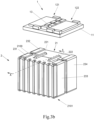
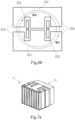
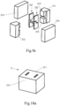
- FIG. 3a is a schematic structural view of a power supply module according to the first embodiment of this disclosure.
- FIG. 3b is an exploded view of the power supply module as shown in FIG. 3a.
- FIG. 3a and 3b show the power supply module according to the first embodiment of this disclosure, and the power supply module includes an integrated power module (IPM) 1, a multi-winding inductor 2 and a plurality of conductive elements.
- IPM integrated power module
- An integrated power module 1 is stacked on a first surface, for example an upper surface of the multi-winding inductor 2 and contains a printed circuit board 11, a first switching unit 121, a second switching unit 122 and a capacitor 13.
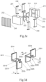
- FIG. 3 is an exploded view of the multi-winding inductor as shown in FIG. 3a .
- the multi-winding inductor 2 of this disclosure includes a magnetic core 21, a first winding 221 and a second winding 222.
- the magnetic core 21 includes a first cover plate 211 and a second cover plate 212 which are arranged oppositely, a first magnetic column 213, a second magnetic column 214, a third magnetic column 215 and a fourth magnetic column 216.
- the first cover plate 211 and the second cover plate 212 are connected with the first magnetic column 213, the second magnetic column 214, the third magnetic column 215 and the fourth magnetic column 216, respectively.
- the first magnetic column 213, the second magnetic column 214, the third magnetic column 215, and the fourth magnetic column 216 each is divided into two symmetric portions by an air gap.
- the first portions of the first magnetic column 213, the second magnetic column 214, the third magnetic column 215, and the fourth magnetic column 216 are connected with the cover plate 211, to form one double-central column E type magnetic core.
- the second portions of the first magnetic column 213, the second magnetic column 214, the third magnetic column 215 and the fourth magnetic column 216 are connected with the cover plate 212, to form another double-central column E type magnetic core. Therefore, the magnetic core in the first embodiment is double-central column EE type magnetic core.
- FIG. 3d is an exploded view of the first winding 221 and the second winding 222 in the multi-winding inductor as shown in FIG. 3c .
- the first winding 221 includes a first portion 2211, a second portion 2212, and a third portion 2213 connected in sequence.
- the first portion 2211 of the first winding 221 is arranged between the first magnetic column 213 and the second magnetic column 214.
- the second portion 2212 of the first winding 221 is arranged between the first magnetic column 213 and the third magnetic column 215.
- the third portion 2213 of the first winding 221 is arranged between the third magnetic column 215 and the fourth magnetic column 216.
- the first portion 2211 of the first winding 221 extends to a first surface 2100 of the magnetic core and forms a first pin 2214 of the multi-winding inductor on the first surface 2100 of the magnetic core.
- the third portion 2213 of the first winding 221 extends to a second surface 2101 of the magnetic core and forms a second pin 2215 of the multi-winding inductor on the second surface 2101 of the magnetic core.
- the first surface 2100 for example, may be a top surface of the magnetic core
- the second surface 2101 for example, may be a bottom surface of the magnetic core.
- the second winding 222 includes a first portion 2221, a second portion 2222 and a third portion 2223 connected in sequence.
- the first portion 2221 of the second winding 222 is arranged between the first magnetic column 213 and the fourth magnetic column 216.
- the second portion 2222 of winding 222 is arranged between the first magnetic column 213 and the third magnetic column 215.
- the third portion 2223 of the second winding 222 is arranged between the third magnetic column 215 and the second magnetic column 214.
- the first portion 2221 of the second winding 222 extends to the first surface 2100 of the magnetic core and forms a third pin 2224 of the multi-winding inductor on the first surface 2100.
- the third portion 2223 of the second winding extends to the second surface 2101 of the magnetic core and forms a fourth pin 2225 of the multi-winding inductor on the second surface 2101.
- a bayonet 2218 is arranged on the first winding 221, and a bayonet 2228 is arranged on the corresponding position of the second winding 222.
- the bayonets are provided on the two windings such that the two windings are arranged crosswise and assembled in an overlapped manner.
- holes may be provided on the first winding 221 and the second winding 222 such that the two windings are arranged crosswise and assembled in an overlapped manner.
- the windings are arranged crosswise, so that the second portions of the two windings are overlapped together, to reduce a length of a magnetic path generated by the current in the second portions of the two windings, and enhance the performance of coupling.
- the first winding and the second winding each is a copper flat conductive element with a width and a thickness.
- the width W1 of the first winding 221 is greater than the thickness T1 thereof.
- the width W2 of the second winding is greater than the thickness T2 thereof.
- a width direction is parallel to the extension direction of the first magnetic column 213 from the first cover plate 211 to the second cover plate 212, that is, a height direction of the magnetic core.
- the first pin 2214 and the third pin 2224 of the multi-winding inductor are arranged on the first surface 2100 of the magnetic core, for example, on the upper surface of the multi-winding inductor.
- the first pin 2214 is connected with a pad of the first switching unit 121 in the integrated power module (corresponding to a node SW1 in FIG. 2 ); and the third pin 2224 is connected with a pad of the second switching unit 122 in the integrated power module (corresponding to a node SW2 in FIG. 2 ), as such, a connection path between the switching unit and the winding of multi-winding inductor is shortest, which is beneficial to reduce impedance and improve efficiency.
- the second pin 2215 of the multi-winding inductor and the fourth pin 2225 of the multi-winding inductor are arranged on the second surface 2101 of the magnetic core, for example, on the lower surface 2101 of the multi-winding inductor, and may be directly connected to the load. Such arrangement is provided such that the path between the output of the power module and the load is shortest, and also is beneficial to reduce the impedance and improve efficiency.
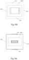
- FIG. 4a is a schematic view showing a pad layout of the first switching unit 121 in the first embodiment.
- the first switching unit 121 and the second switching unit 122 in the integrated power module have rectangular structures.
- the width direction of the first winding 221 and the second winding 222 is consistent with the length direction of the first switching unit 121 or the second switching unit 122.
- the first pin 2214 or the third pin 2224 is basically rectangular in shape, and the length direction of the first pin 2214 or the third pin 2224 is consistent with the length direction of the first switching unit 121 or the second switching unit 122.
- the first switching unit 121 as shown in FIG.
- the first switching unit 121 includes a first switching device S11 and a second switching device S12.
- the first switching device S11 includes an input pad 1212 (corresponding to the Vin in FIG. 2 ) and a switch node pad 1214 (corresponding to the node SW1 in FIG. 2 ).
- the second switching device S12 includes a switch node pad 1214 (corresponding to the node SW1 in FIG. 2 ) and a ground pad 1213 (corresponding to the node GND in FIG. 2 ).
- the input pin1 i.e., the first pin 2214
- the second switching device S22 the input pin1 (i.e., the first pin 2214) of the multi-winding inductor is connected with the first switching device S11 and the second switching device S22. Therefore, the shorter the connected path is, the better the connected area is.
- the first switching unit 121 is rectangular, and the length direction of the first switching unit 121 is consistent with the width direction of the first winding 221, and the width direction of the first winding 221 is parallel to the extension direction of the magnetic column.
- the connection path is shortest and the overlapped area is large, and the connection impedance is small, which is beneficial to improve the efficiency.
- the second switching unit 122 has the same circumstance above.
- the pad structure as shown in FIG. 4b in the case that the width of the winding of the multi-winding inductor is smaller than the thickness thereof, between the first pin 2214 of the multi-winding inductor and the switch node pad 1214, the overlapped area is small and the connection impedance is large, which is harmful to improve efficiency.
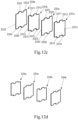
- FIG. 5a is a schematic structural view of a winding of the multi-winding inductor in FIG. 3a ;
- FIG. 5b is a top view of FIG. 5a ;
- FIG. 5c is a schematic structural view of a winding of the multi-winding inductor in another embodiment.
- FIG. 5a and 5c are schematic structural views respectively showing the windings with different width and thickness relationships. In the winding as shown in FIG.
- the width W of the winding is greater than the thickness T thereof, at this time, the size of the winding stacked in the height direction H is small, so the height of the entire winding is small, which is beneficial to reduce the height of the multi-winding inductor.
- the width W of the winding is greater than the thickness T, on one hand, it is beneficial to reduce the connection loss between the winding and the switching unit, on the other hand, it is also beneficial for reducing the height of the multi-winding inductor.
- the width W of the first winding 221 and the second winding 222 after being assembled is the same as the width W1 of one of the two windings, for example the first winding 221, so that the length of the magnetic path (i.e., the first magnetic path) in second portions of the two windings is reduced by half, so as to facilitate the improvement of the coupling efficiency.
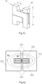
- FIG. 6a is a sectional view of line A-A in the multi-winding inductor in FIG. 3b ; and FIG. 6b is a top view of the multi-winding inductor.
- a current flows in from the first pin 2214 and the third pin 2224 of the multi-winding inductor and flows out from the second pin 2215 and the fourth pin 2225, and a magnetic flux generated by the first winding 221 and the second winding 222 are shown in dotted lines in FIG. 6a and FIG. 6b .
- FIG. 6a shows a first magnetic path formed by the first cover plate 211, the first magnetic column 213, the second cover plate 212 and the third magnetic column 215; wherein ⁇ 1 is a magnetic flux generated by the current in the first winding 221; ⁇ 2 is a magnetic flux generated by the current in the second winding 222; since the magnetic flux ⁇ 1 and the magnetic flux ⁇ 2 have opposite directions, thereby canceling each other and forming a negative coupling.
- FIG. 6b shows a second magnetic path formed by the first cover plate 211, the second magnetic column 214, the second cover plate 212 and the fourth magnetic column 216 of the magnetic core; wherein ⁇ 3 is a magnetic flux generated by the current in the first winding 221; ⁇ 4 is a magnetic flux generated by the current in the second winding 222; since the magnetic flux ⁇ 3 and the magnetic flux ⁇ 4 have the same direction, thereby reinforcing each other and forming a positive coupling.
- the multi-winding inductor When the magnetic fluxes ⁇ 1, ⁇ 2 are greater than the magnetic fluxes ⁇ 3, ⁇ 4, that is, when a reluctance of the first magnetic path is less than a reluctance of the second magnetic path, the multi-winding inductor generally presents a negative coupling relationship, and the first pin and the third pin of the multi-winding inductor are terminals of different magnetic polarity.
- Rm le/( ⁇ e*Ae), wherein Rm is a reluctance, le is an equivalent magnetic path length, ⁇ e is an equivalent permeability, and Ae is an equivalent magnetic sectional area.
- the reluctance Rm of the magnetic core is proportional to the equivalent magnetic path length le of the magnetic path, and is inversely proportional to the equivalent permeability ⁇ e of the magnetic core, and is inversely proportional to the equivalent magnetic sectional area Ae of the magnetic core.
- the difference of the reluctance can be achieved by following methods: firstly, the difference of the reluctances of the magnetic paths can be achieved by adjusting the equivalent permeability of the magnetic path by setting and adjusting the length of the air gap; secondly, the difference of the reluctances of the magnetic paths can be achieved by setting the magnetic permeability of the magnetic materials of the magnetic paths without setting the air gap; thirdly, in the case of the same magnetic materials without setting the air gap, the difference of reluctances of the magnetic paths can be achieved by adjusting a ratio le/Ae between the equivalent magnetic path length and the equivalent magnetic sectional area; fourthly, two or three of the first, second and third methods as set forth above are used in combine.
- the first method as set forth above is adopted to adjust the equivalent permeability of magnetic path by setting the air gap, that is, setting the air gap on at least one of the first magnetic column 213 and the third magnetic column 215 of the first magnetic path, and setting the air gap on at least one of the second magnetic column 214 and the fourth magnetic column 216 of the second magnetic path, and thereby the total length of the air gaps in the first magnetic path is less than the total length of the air gaps in the second magnetic path; or merely setting the air gap on at least one of the second magnetic column 214 and the fourth magnetic column 216 of the second magnetic path without setting the air gap in the first magnetic column 213 and the third magnetic column 215 of the first magnetic path, thereby realizing that the reluctance in the first magnetic path is less than the reluctance in the second magnetic path, therefore, the magnetic fluxes ⁇ 1, ⁇ 2 are greater than the magnetic fluxes ⁇ 3, ⁇ 4 so as to achieve the negative coupling.
- table 1 is an arrangement in the first embodiment, in which the air gap of the first magnetic column and the third magnetic column is different from the air gap of the second magnetic column and the fourth magnetic column in length, thereby obtaining the coupling relationship of the negative coupling, the positive coupling and the non-coupling, respectively.
- the materials with various magnetic permeability are used such that, the reluctance in the path of the magnetic fluxes ⁇ 1, ⁇ 2 is less than the reluctance in the path of the magnetic fluxes ⁇ 3, ⁇ 4, so as to achieve an object of negative coupling.
- a plurality of conductive elements is arranged around the magnetic core 21.
- the conductive element includes a first end and a second end, the first end forms a fifth pin on the first surface, for example the upper surface of the magnetic core; and the second end forms a sixth pin on the second surface, for example the lower surface of the magnetic core.
- a plurality of conductive elements includes, for example, a signal connection assembly and at least two groups of power connection assemblies.
- At least two groups of power connection assemblies are respectively arranged on the first side and the second side of the multi-winding inductor, and the first side and the second side are arranged oppositely; and the signal connection assembly is arranged on the third and/or fourth sides of the multi-winding inductor, wherein the third side and the fourth side are arranged oppositely and are connected between the first side and the second side.
- At least two groups of the power connection assemblies include a first power connection assembly on the first side of the magnetic core and a second power connection assembly on the second side of the magnetic core.
- the first power connection assembly includes a first input conductive element 231 and a first ground conductive element 232; and the second power connection assembly includes a second input conductive element 233 and a second ground conductive element 234.
- the first input conductive element 231 and the first ground conductive element 232 are arranged on the outer side of the second magnetic column 214, and the second input conductive element 233 and the second ground conductive element 234 are arranged on the outer side of the fourth magnetic column 216.
- the signal connection assembly includes a plurality of signal conductive elements 241 that are arranged on the third side of the magnetic core, for example the outer side of the second cover plate 212.
- input connecting wires 104 and 105 in FIG. 2 correspond to input conductive elements 231 and 233 in FIG. 3c , respectively; and ground connecting wires 106 and 107 in FIG. 2 correspond to ground conductive elements 232 and 234 in FIG. 3c , respectively.
- the input connecting wire 104 and the ground connecting wire 106 form a loop through the first switching unit 101 and the input power supply.
- the existence of the loop can produce a loop parasitic inductance, if the loop parasitic inductance resonates with an input capacitor, the efficiency of the power supply system can be affected.
- the first input conductive element 231 and the first ground conductive element 232 are arranged side by side in the first embodiment, to minimize a distance between the first input conductive element 231 and the first ground conductive element 232 as possible, the smaller the distance, the smaller the area of the loop, the less the parasitic inductance in the loop, thereby being beneficial to the improvement of the efficiency.
- the second input conductive element 233 and the second ground conductive element 234 are arranged side by side, to minimize the distance between them as possible.
- the conductive elements all form pads on the first surface and the second surface of the magnetic core 21, that is, the fifth pin and the sixth pin as mentioned above, for power connection or signal transmission between the integrated power module 1 and the load. In other embodiments, the conductive elements may be arranged in a different way.
- the first and third pins of the multi-winding inductor are arranged on the first surface of the multi-winding inductor, and the second and fourth pins of the multi-winding inductor are arranged on the second surface of the multi-winding inductor, so that the four sides of the multi-winding inductor all may be used to set the power connection assembly and the signal connection assembly.
- the arrangement of the magnetic core and the winding provide sufficient space for the setting of the input connection assembly and the signal connection assembly of the power supply module.
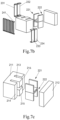
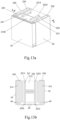
- FIG. 7a is an assembling view of the power supply module according to the second embodiment of this disclosure, in which an integrated power module is omitted; and FIG. 7b is an exploded view of FIG.7a ; FIG.7c is an exploded view of the multi-winding inductor in FIG.7a .
- the difference of the power supply module of the second embodiment in comparison with that of the first embodiment is that the specific structure of the multi-winding inductor 2 is slightly different.
- a multi-winding inductor in the second embodiment of the power supply module includes a magnetic core 21 and a winding.
- the magnetic core 21 includes a first cover plate 211 and a second cover plate 212 arranged oppositely, and a first magnetic column 213, a second magnetic column 214, a third magnetic column 215 and a fourth magnetic column 216 arranged between the first cover plate 211 and the second cover plate 212.
- the second cover plate 212 and the magnetic columns are separated by the air gap to form an I-type magnetic core portion.
- the first cover plate 211 is connected with the first magnetic column 213, the second magnetic column 214, the third magnetic column 215 and the fourth magnetic column 216, to form a magnetic core portion with double-central column E type structure. Therefore, the magnetic core structure in the second embodiment is double-central column EI type magnetic core.
- the winding in the second embodiment includes the first winding 221 and the second winding 222, which is basically the same with the winding structure as illustrated in FIG. 3d in the first embodiment.
- the width of the winding is greater than the thickness thereof, a welding area of the first pin of the winding and the pad of the switching unit is large, and the connection impedance is minimized.
- the first pin 2214 of the multi-winding inductor and the third pin 2224 of the multi-winding inductor are arranged on the first surface of the multi-winding inductor, and are directly connected with the switch node pad of the first switching unit 121 and the switch node pad of the second switching unit 122, as such, the path between the switching unit and the multi-winding inductor is shortest, thereby reducing the impedance and improving the efficiency.
- the second pin 2215 of the multi-winding inductor and the fourth pin 2225 of the multi-winding inductor are arranged on the second surface of the multi-winding inductor, and are directly connected with the load, as such, the path between the output of the VRM and the load is shortest, thereby reducing the impedance and improving the efficiency.
- the position relationship between the windings and the first magnetic column 213, the second magnetic column 214, the third magnetic column 215 and the fourth magnetic column 216 in the second embodiment is basically the same as that in the first embodiment.
- the current in the two windings respectively form magnetic fluxes ⁇ 1, ⁇ 2 in the first magnetic path; the current in the two windings respectively form the magnetic fluxes ⁇ 3, ⁇ 4 in the second magnetic path; the direction of the magnetic flux ⁇ 1 is opposite to the of the magnetic flux ⁇ 2; the directions of the magnetic fluxes ⁇ 3 and ⁇ 4 are the same.
- the multi-winding inductor When the magnetic fluxes ⁇ 1, ⁇ 2 are greater than the magnetic fluxes ⁇ 3, ⁇ 4, the multi-winding inductor generally realizes the negative coupling relationship, and the first pin and the third pin of the multi-winding inductor are terminals of different magnetic polarity; when the magnetic fluxes ⁇ 1, ⁇ 2 are less than the magnetic fluxes ⁇ 3, ⁇ 4, the multi-winding inductors generally realize the positive coupling relationship, and the first pin and the third pin of the multi-winding inductor are the dotted terminals(terminals of same magnetic polarity); when the magnetic fluxes ⁇ 1, ⁇ 2 are equal to the magnetic fluxes ⁇ 3, ⁇ 4, the multi-winding inductor generally realizes the non-coupling relationship.
- the air gap in the first magnetic column 213 and the third magnetic column 215 is smaller than the air gap in the second magnetic column 214 and the fourth magnetic column 216 such that the reluctance in the path of the magnetic fluxes ⁇ 1, ⁇ 2 is less than the reluctance in the path of the magnetic fluxes ⁇ 3, ⁇ 4. Therefore, the magnetic fluxes ⁇ 1, ⁇ 2 are greater than the magnetic fluxes ⁇ 3, ⁇ 4, so as to achieve the negative coupling.
- the conductive elements 231, 232, 233 and 234 in the second embodiment are respectively arranged on a side column of the double-central column E type magnetic core, that is, on the outer side of the second magnetic column 214 and the fourth magnetic column 216.
- the first input conductive element 231 and the first ground conductive element 232 are arranged symmetrical to the second input conductive element 233 and the second ground conductive element 234 on the opposite sides of the multi-winding inductor.
- the signal conductive element 241 is arranged on the outer side of the first cover plate 211, that is, on the outer side of the cover plate of the double-central column E type magnetic core.
- the conductive elements each form a pad on the first and second surfaces of the magnetic core, for the power connection or the signal transmission between the integrated power supply module 1 and the load.
- the magnetic core is arranged in a structural form of the double-central column E type magnetic core and the I type cover plate, the position of the air gap moves from the central position of the magnetic core in the first embodiment to one side, because the conductive elements when setting need to avoid the air gap, relative to the four conductive elements in the first embodiment, and only two conductive elements 232, 234 in the second embodiment need to avoid the air gap, flux leakage of the air gap and eddy current loss of an edge flux on the conductive elements are reduced.
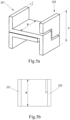
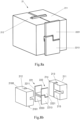
- FIG. 8a is a schematic view of a multi-winding inductor of the power supply module according to the third embodiment of this disclosure.
- FIG. 8b is an exploded view of the multi-winding inductor according to the third embodiment of this disclosure.
- the multi-winding inductor includes a magnetic core and a winding.
- the magnetic core has only three magnetic columns and two cover plates.
- the structure of the magnetic core is similar to the magnetic core formed by cutting off the fourth magnetic column 216 and part of the cover plates as shown in FIG. 3c .
- the magnetic core includes the first cover plate 211 and the second cover plate 212 arranged oppositely, and the first magnetic column 213, the second magnetic column 214 and the third magnetic column 215 orderly arranged counterclockwise between the first cover plate 211 and the second cover plate 212.
- the winding assembly of the multi-winding inductor includes a first winding 221 and a second winding 222 arranged crosswise, which is the same as that in the first embodiment, and is beneficial to reduce a volume of the multi-winding inductor.
- the first winding 221 and the second winding 222 each includes a first portion, a second portion and a third portion, wherein the first portion and the third portion of each of the windings are connected by the second portion.
- the first winding is provided with a notch or a hole
- the second winding is provided with a notch or a hole
- the first winding and the second winding are arranged crosswise through the notch or the hole, so that the second portion 2212 of the first winding 221 and the second portion 2222 of the second winding 222 are overlapped.
- the first magnetic column 213 is arranged between the first portion 2211 of the first winding 221 and the first portion 2221 of the second winding 222.
- the second magnetic column 214 is arranged on one side of the first portion 2211 of the first winding 221 and the third portion 2223 of the second winding 222.
- the third magnetic column 215 is arranged between the third portion 2213 of the first winding 221 and the third portion 2223 of the second winding 222.
- the first portion 2211 of the first winding 221 extends to the first surface 2100 of the magnetic core so as to form the first pin 2214 of the inductor; the third portion 2213 of the first winding 221 extends to the second surface 2101 of the magnetic core so as to form the second pin 2215 of the inductor; and the first portion 2221 of the second winding 222 extends to the first surface 2100 of the magnetic core so as to form the third pin 2224 of the inductor; and the third portion 2223 of the second winding 222 extends to the second surface 2101 of the magnetic core so as to form the fourth pin 2225 of the inductor.
- the first surface 2100 and the second surface 2101 of the magnetic core are arranged oppositely.
- the current in the first winding 221 flows in from the first pin 2214 of the first surface, and the current in the second winding 222 flows in from the third pin 2224 of the first surface.
- the magnetic flux in the path formed by the first cover plate 211, the first magnetic column 213, the second cover plate 212 and the third magnetic column 215 is greater than the magnetic flux in the path formed by the first cover plate 211, the first magnetic column 213, the second cover plate 212 and the second magnetic column 214, or is greater than the magnetic flux in the path formed by the first cover plate 211, the third magnetic column 215, the second cover plate 212 and the second magnetic column 214, the multi-winding inductor realizes the negative coupling relationship, and the first pin 2214 and the third pin 2224 of the multi-winding inductor are terminals of different magnetic polarity to each other.
- the multi-winding inductor in the third embodiment has only three magnetic columns, so that the equivalent magnetic path sectional area of each of the magnetic columns is larger and the loss of the magnetic core is reduced, at the same time, the magnetic core has a simple structure and is easy to manufacture.
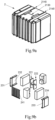
- FIG. 9a is an assembling view of the power supply module according to the fourth embodiment of this disclosure, in which an integrated power module is omitted;
- FIG. 9b is an exploded view of FIG. 9a ;
- FIG. 9c is an exploded view of the multi-winding inductor in FIG. 9a .
- the difference between the power supply modules of the fourth embodiment in comparison with that of the first embodiment lies in the specific structure of the multi-winding inductor 2.
- a magnetic core of a multi-winding inductor in the fourth embodiment includes a first cover plate 211, a second cover plate 212, a first magnetic column 213, a second magnetic column 214, a third magnetic column 215 and a fourth magnetic column 216.
- the first cover plate 211, the second cover plate 212, the first magnetic column 213, the second magnetic column 214, the third magnetic column 215, and the fourth magnetic column 216 are assembled together.
- the second magnetic column 214 and the fourth magnetic column 216 are separated by the first air gap 2140 and the second air gap 2160, respectively, to form two I type magnetic core structures.
- Each of the first magnetic column 213 and the third magnetic column 215 is divided into two symmetrical portions by the third air gap 2130.
- the first portions of the first magnetic column 213 and the third magnetic column 215 are connected with the first cover plate 211 to form a U-shaped magnetic core structure, and the second portions of the first magnetic column 213 and the third magnetic column 215 are connected with the second cover plate 212 to form a U-shaped magnetic core structure.
- the first cover plate 211, the second cover plate 212, the first magnetic column 213 and the third magnetic column 215 are divided into two symmetrical U-shaped magnetic core structures by the third air gap 2130. Therefore, the magnetic core in the fourth embodiment is IUUI type magnetic core.
- the first pin 2214 of the multi-winding inductor and the third pin 2224 of the multi-winding inductor are arranged on the first surface of the multi-winding inductor, and are directly connected with the pad of the first switching unit 121 and the pad of the second switching unit 122, as such, the connection path between the switching unit and the windings of the multi-winding inductor is short, to facilitate reducing the impedance and improving the efficiency.
- the second pin 2215 of the multi-winding inductor and the fourth pin 2225 of the multi-winding inductor are arranged on the second surface of the multi-winding inductor, and are directly connected with the load, as such, the path between the output of the power supply system and the load is short, to facilitate reducing the impedance and improving the efficiency.
- the position relationship between the windings and the first magnetic column 213, the second magnetic column 214, the third magnetic column 215, and the fourth magnetic column 216 in the fourth embodiment is basically the same as that in the first embodiment.
- the current in the two windings respectively form magnetic fluxes ⁇ 1, ⁇ 2 in the first magnetic path (i.e., the magnetic flux path formed by the first cover plate 211, the first magnetic column 213, the second cover plate 212 and the third magnetic column 215); and the current in the two windings respectively form magnetic fluxes ⁇ 3, ⁇ 4 in the second magnetic path (i.e., the magnetic flux path formed by the first cover plate 211, the second magnetic column 214, the second cover plate 212 and the fourth magnetic column 216).
- the magnetic fluxes ⁇ 1 and ⁇ 2 have the same size and opposite directions; and the magnetic fluxes ⁇ 3 and ⁇ 4 have the same size and the same direction.
- the multi-winding inductor realizes the negative coupling relationship, and the first pin and the third pin of the multi-winding inductor are terminals of different magnetic polarity to each other;
- the magnetic fluxes ⁇ 1, ⁇ 2 are less than the magnetic fluxes ⁇ 3, ⁇ 4, the multi-winding inductor realizes the positive coupling relationship, and the first pin and the third pin of the multi-winding inductor are dotted terminals(terminals of same magnetic polarity) to each other; and when the magnetic fluxes ⁇ 1, ⁇ 2 are equal to the magnetic fluxes ⁇ 3, ⁇ 4, the multi-winding inductor realizes the non-coupling relationship.
- the air gap in the first magnetic column 213 and the third magnetic column 215 is smaller than the air gap in the second magnetic column 214 and the fourth magnetic column 216, such that the reluctance in the path of the magnetic fluxes ⁇ 1, ⁇ 2 is less than the reluctance in the path of the magnetic fluxes ⁇ 3, ⁇ 4. Therefore, the magnetic fluxes ⁇ 1, ⁇ 2 are greater than the magnetic fluxes ⁇ 3, ⁇ 4, so as to achieve the negative coupling.
- a UU structure magnetic core composed of the first cover plate 211, the second cover plate 212, the first magnetic column 213 and the third magnetic column 215 is set as the magnetic material with high magnetic permeability, for example a ferrite.
- An II type magnetic core structure formed by the second magnetic column 214 and the fourth magnetic column 216 is set as the magnetic material with low magnetic permeability, for example a powder core material with an insulation coating.
- the magnetic material of the UU type magnetic core has the high magnetic permeability and the low reluctance, and the magnetic fluxes ⁇ 1, ⁇ 2 therein are large; the magnetic materials of the two I type magnetic cores have low magnetic permeability and the high reluctance, and the magnetic fluxes ⁇ 3, ⁇ 4 therein are small. It is possible to realize the requirement that the magnetic fluxes ⁇ 1, ⁇ 2 are greater than the magnetic fluxes ⁇ 3, ⁇ 4.
- the UU type magnetic core uses the magnetic material with the high magnetic permeability, which can make the coupling of negative coupling multi-winding inductor better.
- the two I type magnetic cores use the magnetic material with the low magnetic permeability, which can improve a saturation current capability of the negative coupling multi-winding inductor.
- the conductive elements 231, 232, 233 and 234 in the fourth embodiment are arranged on the outer sides of the second magnetic column 214 and the fourth magnetic column 216, respectively.
- the first input conductive element 231 and the first ground conductive element 232 are arranged symmetrical to the second input conductive element 233 and the second ground conductive element 234 on the two opposite sides of the multi-winding inductor.
- the signal conductive element 241 is arranged on the side of the second cover plate 212.
- the input conductive element, the ground conductive element and the signal conductive element each may form pads on the first and second surfaces, for the power connection or the signal transmission between the integrated power supply module and the inductor and between the load and the inductor.
- the magnetic core is set in the form of IUUI structure
- the conductive elements can completely avoid the air gap and reduce the loss of the magnetic flux at the edge of the air gap on the conductive element, and the width of the conductive element can be wider to reduce the DC impedance of the conductive element, and the IUUI type magnetic core structure is also easier to be molded.
- FIG. 10a is a schematic structural view of another multi-winding inductor according to the fifth embodiment of this disclosure.
- FIG. 10b is a perspective view of the multi-winding inductor in FIG. 10a .
- FIG. 10c is a sectional view taken along the line B-B in FIG. 10b .
- FIG. 10d is a top view of FIG.10b .
- FIG. 10e is a sectional view taken along the line C-C in FIG. 10b .
- the magnetic core thereof is a magnetic material with low magnetic permeability with an insulation coating, for example, the magnetic powder material, etc.
- the inductor is formed by pressing the winding and the magnetic material together and there is no air gap provided in the magnetic core.
- the multi-winding inductor realizes the negative coupling by setting the equivalent sectional area and the equivalent magnetic path length of the magnetic columns.
- the magnetic core is an overall structure integrally formed.
- the magnetic core is separated to form the first cover plate 211, the second cover plate 212, the first magnetic column 213, the second magnetic column 214, the third magnetic column 215, and the fourth magnetic column 216 by the winding.
- the current in the two windings respectively form the magnetic fluxes ⁇ 1, ⁇ 2 in the first magnetic path (i.e., the magnetic flux path formed by the first cover plate 211, the first magnetic column 213, the second cover plate 212 and the third magnetic column 215); and the current in the two windings form magnetic fluxes ⁇ 3, ⁇ 4 in the second magnetic path (i.e., the magnetic flux path formed by the first cover plate 211, the second magnetic column 214, the second cover plate 212 and the fourth magnetic column 216).
- the first magnetic path has an equivalent magnetic path sectional area 23S1 and an equivalent magnetic path length 24L1.
- the second magnetic path has an equivalent magnetic path sectional area 23S2 and an equivalent magnetic path length 24L2.
- a ratio 24L1/23S1 of the equivalent magnetic path length to the equivalent magnetic path section area of the magnetic flux in the first magnetic path is less than a ratio 24L2/23S2 of the equivalent magnetic path length to the equivalent magnetic path section area of the magnetic flux in the second magnetic path, the magnetic fluxes ⁇ 1, ⁇ 2 are greater than the magnetic fluxes ⁇ 3, ⁇ 4 to achieve the negative coupling.
- the ratio 24L1/23S1 of the equivalent magnetic path length to the equivalent magnetic path section area of the magnetic flux in the first magnetic path is less than the ratio 24L2/23S2 of the equivalent magnetic path length to the equivalent magnetic path sectional area of the magnetic flux in the second magnetic path to achieve the negative coupling.
- FIG. 11a is an assembling view of the power supply module according to the sixth embodiment of this disclosure, in which an integrated power module is omitted.
- FIG. 11b is an exploded view of FIG. 11a .
- FIG. 11c is an exploded view of the first power connection assembly in the power supply module in FIG. 11a .
- FIG. 11d is an exploded view of the second power connection assembly in the power supply module in FIG. 11a .
- the difference of the power supply module of the sixth embodiment in comparison with that of the first embodiment lies in the specific structure of the conductive element.
- a plurality of conductive elements of the power supply module includes at least two groups of power connection assemblies.
- FIG. 11a shows two groups: the first power connection assembly and the second power connection assembly provided on opposite sides of the magnetic core.
- the first power connection assembly includes a first input conductive element 231 and a first ground conductive element 232; and the second power connection assembly includes a second input conductive element 233 and a second ground conductive element 234.
- the first input conductive element 231 overlaps at least partially with the first ground conductive element 232, and the second input conductive element 233 overlaps at least partially with the second ground conductive element 234.
- the first input conductive element 231 includes a first portion 2311, a second portion 2312, and a third portion 2313 which are connected in sequence.
- the first ground conductive element 232 includes a first portion 2321, a second portion 2322 and a third portion 2323 which are connected in sequence.
- the first portion 2311 of the first input conductive element 231 is arranged on a left side of an upper end of the second portion 2312 of the first input conductive element 231.
- the first portion 2321 of the first ground conductive element 232 is arranged on a right side of an upper end of the second portion 2322 of the first ground conductive element 232.
- the first portion 2311 of the first input conductive element 231 and the first portion 2321 of the first ground conductive element 232 respectively form pins on the first surface of the magnetic core, for connecting the integrated power module.
- the third portion 2313 of the first input conductive element 231 is arranged on a right side of a lower end of the second portion 2312 of the first input conductive element 231.
- the third portion 2323 of the first ground conductive element 232 is arranged on a left side of a lower end of the second portion 2322 of the first ground conductive element 232.
- the third portion 2313 of the first input conductive element 231 and the third portion 2323 of the first ground conductive element 232 form pins on the second surface of the magnetic core respectively, for connecting a customer's mainboard.
- the second portion 2312 of the first input conductive element 231 overlaps with the second portion 2322 of the first ground conductive element 232, and the two portions are insulated and have a short interval, so that a loop area between the input conductive elements in this section is small, and the parasitic inductance is small.
- the first portion 2311 of the first input conductive element 231 is staggered and non-overlapping with the first portion 2321 of the first ground conductive element 232 on the first surface of the magnetic core
- the third portion 2313 of the first input conductive element 231 is staggered and non-overlapping with the third portion 2323 of the first ground conductive element 232, such that the magnetic flux in the loop formed by the first portions 2311, 2321 on the first surface and the magnetic flux in the loop formed by the third portions 2313, 2323 on the second surface offset each other, thereby further reducing the parasitic inductance of the whole loop.
- the second power connection assembly includes a second input conductive element 233 and a second ground conductive element 234.
- the structure of the second input conductive element 233 and the second ground conductive element 234 is basically the same as that of the conductive elements 231, 232 as shown in FIG. 11c .
- the second input conductive element 233 includes a first portion 2331, a second portion 2332 and a third portion 2333 which are connected in sequence.
- the second ground conductive element 234 includes a first portion 2341, a second portion 2342 and a third portion 2343 which are connected in sequence.
- the first portion 2331 of the second input conductive element 233 is staggered and non-overlapping with the first portion 2341 of the second ground conductive element 234 on the first surface of the magnetic core
- the third portion 2333 of the second input conductive element 233 is staggered and non-overlapping with the third portion 2343 of the second ground conductive element 234 on the second surface of the magnetic core, such that the magnetic flux in the loop formed by the first portions 2331, 2341 on the first surface and the magnetic flux in the loop formed by the third portions 2333, 2343 on the second surface offset each other, thereby further reducing the parasitic inductance of the whole loop.
- the second portions of the conductive elements are overlapped and the first portions and the third portions are staggered to reduce the parasitic inductance in the loop of the conductive elements, so as to improve the efficiency.
- FIG. 12a is an assembling view of the power supply module according to the seventh embodiment of this disclosure, in which an integrated power module is omitted;
- FIG. 12b is an exploded view of FIG. 12a ;
- FIG. 12c is an exploded view of the first power connection assembly in the power supply module in FIG. 12a .
- FIG. 12d is an exploded view of the second power connection assembly in the power supply module in FIG. 12a .
- the difference of the power supply module of the seventh embodiment in comparison with the first embodiment lies in the specific structure of the conductive element.
- the first power connection assembly includes a first input conductive element 231a, a second input conductive element 231b, a first ground conductive element 232a, and a second ground conductive element 232b.
- the shape of the first input conductive element 231a is same as the shape of the second input conductive element 231b.
- Each of the first input conductive element 231a and the second input conductive element 231b contains a first portion 2311, a second portion 2312, a third portion 2313, a fourth portion 2314 and a fifth portion 2315.
- first portion 2311 and the second portion 2312 are connected to the upper side of the third portion 2313
- fourth portion 2314 and a fifth portion 2315 are connected to the lower side of the third portion 2313.
- the shape of the first ground conductive element 232a is same as the shape of the second ground conductive element 232b.
- Each of the first ground conductive element 232a and the second ground conductive element 232b contains a first portion 2321, a second portion 2322, a third portion 2323, a fourth portion 2324 and a fifth portion 2325.
- the first portion 2321 and the second portion 2322 are connected to the upper side of the third portion 2323, the fourth portion 2324 and a fifth portion 2325 are connected to the lower side of the third portion 2323.
- the input conductive element and the ground conductive element are alternatively disposed.
- the first input conductive element 231a, the first ground conductive element 232a, the second input conductive element 231b and the second ground conductive element 232b are disposed in sequence.
- the first portions 2311 and the second portions 2312 of the first input conductive element 231a and the second input conductive element 231b are staggered and non-overlapping with the first portions 2321 and the second portions 2322 of the first ground conductive element 232a and the second ground conductive element 232b on the first surface of the magnetic core, and each of them forms pin on the first surface of the magnetic core.
- the fourth portions 2314 and the fifth portions 2315 of the first input conductive element 231a and the second input conductive element 231b are staggered and non-overlapping with the fourth portions 2324 and the fifth portions 2325 of the first ground conductive element 232a and the second ground conductive element 232b on the second surface of the magnetic core, and each of them forms pin on the second surface of the magnetic core.
- the third portion 2313 of the first input conductive element 231a, the third portion 2323 of the first ground conductive element 232a, the third portion 2313 of the second input conductive element 231b, and the third portion 2323 of the second ground conductive element 232b are overlapped.
- the alternative arrangement of the input conductive element and the ground conductive element helps to reduce the parasitic inductance, and generally such alternative arrangement of the multi-layer conductive elements can be easily achieved by a printed circuit board (PCB) process.
- PCB printed circuit board
- the second power connection assembly includes a third input conductive element 233a, a fourth input conductive element 233b, a third ground conductive element 234a and a fourth ground conductive element 234b.
- the setting mode of the third input conductive element 233a, the fourth input conductive element 233b, the third ground conductive element 234a and the fourth ground conductive element 234b is basically the same as the setting mode of the first input conductive element 231a, the second input conductive element 231b, the first ground conductive element 232a and the second ground conductive element 232b as shown in FIG. 12c , which will not be described herein.
- FIG. 13a is an assembling view of the power supply module according to the eighth embodiment of this disclosure, in which an integrated power module is omitted;
- FIG. 13b is a sectional view taken along the line D-D in FIG. 13a ;
- FIG. 13c is a schematic structural view of a bendable substrate without being folded in FIG. 13a ;
- FIG. 13d is a schematic structural view at another angle of a bendable substrate without being folded in FIG. 13a .
- the multi-winding inductor structure in the power supply module of the eighth embodiment is basically the same as that in the first embodiment, including a magnetic core and a winding.
- the magnetic core includes a first cover plate 211 and a second cover plate 212 arranged oppositely, and a first magnetic column 213, a second magnetic column 214, a third magnetic column 215 and a fourth magnetic column 216 connected to the first cover plate 211 and the second cover plate 212.
- the winding includes a first winding 221 and a second winding 222 arranged crosswise.
- the first winding 221 forms a first pin 2214 on the first surface of the magnetic core and a second pin 2215 on the second surface of the magnetic core, respectively; and the second winding 222 forms a third pin 2224 on the first surface of the magnetic core and a fourth pin 2225 on the second surface of the magnetic core, respectively.
- the difference of the power supply module of the eighth embodiment in comparison with that of the first embodiment lies in further including a bendable substrate, on which the conductive elements and the like are arranged.
- the bendable substrate includes a bottom plate 51, a first side plate 52, a second side plate 53 and a third side plate 54, which are formed by bending and extending the sides of the bottom plate 51.
- the first side plate 52 and the second side plate 53 are arranged oppositely.
- the first side plate 52 is attached to the outer side of the fourth magnetic column 216 of the magnetic core
- the second side plate 53 is attached to the outer side of the second magnetic column 214 of the magnetic core
- the third side plate 54 is attached to the outer side of the second cover plate 212 or the first cover 211 of the magnetic core.
- the upper end portion of the first side plate 52 and the upper end portion of the second side plate 53 extend to the first surface 2100 of the magnetic core so as to form a first extension 520 and a second extension 530, respectively.
- the bottom plate 51 of the bendable substrate is provided with the second pin 2215 and the fourth pin 2225.
- the lower end portion of the first winding 221 may be connected to the second pin 2215 through a wiring inside the bottom plate 51 of the bendable substrate; a lower end portion of the second winding 222 may be connected to the fourth pin 2225 through the wiring inside the bottom plate 51 of the bendable substrate.
- a signal conductive element 241 in the power supply module of the eighth embodiment may be directly arranged on the third side plate 54.
- a first power connection assembly including a first input conductive element 231 and a first ground conductive element 232 may be directly arranged on the first side plate 52.
- a second power connection assembly including a second input conductive element 233 and a second ground conductive element 234 may be arranged directly on the second side plate 53.
- An output capacitor 60 may also be arranged on the bottom plate 51. The output capacitor 60 is located between the bottom plate 51 and the magnetic core.
- the input conductive element, the ground conductive element and the signal conductive element may be formed simultaneously on the bendable substrate in advance, so that the conductive element can achieve high accuracy, including a dimensional accuracy and a relative position accuracy.
- the bendable substrate is made by a PCB process or a flexible PCB process which can achieve the high dimensional accuracy and the relative position accuracy.
- the output capacitor is arranged between the lower surface of the multi-winding inductor and the bendable substrate, so that the number of the output capacitors on the user mainboard can be reduced, to save the space occupied by the output capacitors on the user mainboard, and also shorten a distance between the power supply module's output and the load, thereby reducing the transmission loss between the power supply module and the load, and improving the efficiency of the power supply module.
- the input capacitor between the lower surface of the multi-winding inductor and the bendable substrate.
- the input capacitors are integrated into the multi-winding inductor to increase the number of the input capacitors, reduce a resonance between the input capacitor and the parasitic inductance, so as to reduce the loss and improve the efficiency.
- the capacitors can also be arranged between the upper surface of the multi-winding inductor and the bendable substrate like between the lower surface of the multi-winding inductor and the bendable substrate.
- first and second are merely used for the purpose of description and cannot be interpreted to indicate or imply relative importance;
- a plurality of refers to two or more, unless otherwise explicitly defined;
- install, “connect with”, “connect to” and “fix” shall be broadly understood, for example, “connect to” may be a fixed connection, a detachable connection, or an integrated connection; “connect with” may be direct connection or indirect connection through an intermediate media.
- connect to may be a fixed connection, a detachable connection, or an integrated connection;
- connect with may be direct connection or indirect connection through an intermediate media.
Landscapes
- Engineering & Computer Science (AREA)
- Power Engineering (AREA)
- Chemical & Material Sciences (AREA)
- Composite Materials (AREA)
- Coils Of Transformers For General Uses (AREA)
- Coils Or Transformers For Communication (AREA)
Claims (27)
- Mehrfachwicklungsdrossel, umfassend:einen Magnetkern (21), umfassend eine erste Abdeckplatte (211), eine zweite Abdeckplatte (212) und vier Magnetsäulen, wobei die erste Abdeckplatte (211) und die zweite Abdeckplatte (212) gegenüberliegend angeordnet sind, die vier Magnetsäulen umfassend eine erste Magnetsäule (213), eine zweite Magnetsäule (214), eine dritte Magnetsäule (215) und eine vierte Magnetsäule (216), die geordnet gegen den Uhrzeigersinn angeordnet sind, und wobei zwei Enden von jeder der vier Magnetsäulen jeweils mit der ersten Abdeckplatte (211) und der zweiten Abdeckplatte (212) verbunden sind;eine Wicklungsanordnung umfassend mindestens eine erste Wicklung (221) und eine zweite Wicklung (222), jede von der ersten Wicklung (221) und der zweiten Wicklung (222) umfassend einen ersten Abschnitt, einen zweiten Abschnitt und einen dritten Abschnitt; wobei der erste Abschnitt und der dritte Abschnitt durch den zweiten Abschnitt in jeder von der ersten Wicklung (221) und der zweiten Wicklung (222) verbunden sind;der erste Abschnitt (2211) der ersten Wicklung (221) zwischen der ersten Magnetsäule (213) und der zweiten Magnetsäule (214) angeordnet ist,der dritte Abschnitt (2213) der ersten Wicklung (221) zwischen der dritten Magnetsäule (215) und der vierten Magnetsäule (216) angeordnet ist,der erste Abschnitt (2221) der zweiten Wicklung (222) zwischen der vierten Magnetsäule (216) und der ersten Magnetsäule (213) angeordnet ist, undder dritte Abschnitt (2223) der zweiten Wicklung (222) zwischen der zweiten Magnetsäule (214) und der dritten Magnetsäule (215) angeordnet ist,wobei sich der erste Abschnitt (2211) der ersten Wicklung (221) zu einer ersten Oberfläche (2100) des Magnetkerns (21) erstreckt und einen ersten Stift (2214) der Mehrfachwicklungsdrossel auf der ersten Oberfläche (2100) des Magnetkerns (21) bildet; sich der erste Abschnitt (2221) der zweiten Wicklung (222) zu der ersten Oberfläche (2100) des Magnetkerns (21) erstreckt und einen dritten Stift (2224) der Mehrfachwicklungsdrossel auf der ersten Oberfläche (2100) des Magnetkerns (21) bildet; undwobei jede von der ersten Wicklung (221) und der zweiten Wicklung (222) ein Flachdraht mit einer Breite und einer Stärke ist, wobei die Stärke geringer ist als die Breite, wobei eine Breitenrichtung parallel zu einer Erstreckungsrichtung der ersten Magnetsäule (213) ist,wobei die erste Wicklung (221) und die zweite Wicklung (222) kreuzweise sind, sodass der zweite Abschnitt (2212) der ersten Wicklung (221) und der zweite Abschnitt (2222) der zweiten Wicklung (222) überlappt sind.
- Mehrfachwicklungsdrossel nach Anspruch 1, wobei die erste Wicklung (221) mit einer Kerbe oder einem Loch versehen ist, die zweite Wicklung (222) mit einer Kerbe oder einem Loch versehen ist und die erste Wicklung (221) und die zweite Wicklung (222) kreuzweise durch die Kerbe oder das Loch sind.
- Mehrfachwicklungsdrossel nach Anspruch 1, wobei sich der dritte Abschnitt (2213) der ersten Wicklung (221) zu einer zweiten Oberfläche (2101) des Magnetkerns (21) erstreckt, um einen zweiten Stift (2215) der Mehrfachwicklungsdrossel zu bilden; und sich der dritte Abschnitt (2223) der zweiten Wicklung (222) zu einer zweiten Oberfläche (2101) des Magnetkerns (21) erstreckt, um einen vierten Stift (2225) der Mehrfachwicklungsdrossel zu bilden.
- Mehrfachwicklungsdrossel nach Anspruch 1, wobei die erste Magnetsäule (213), die erste Abdeckplatte (211), die dritte Magnetsäule (215) und die zweite Abdeckplatte (212) einen ersten magnetischen Pfad bilden; die erste Abdeckplatte (211), die zweite Magnetsäule (214), die zweite Abdeckplatte (212) und die vierte Magnetsäule (216) einen zweiten magnetischen Pfad bilden; und eine Gesamtreluktanz des ersten magnetischen Pfads kleiner ist als eine Gesamtreluktanz des zweiten magnetischen Pfads.
- Mehrfachwicklungsdrossel nach Anspruch 1, wobei die erste Magnetsäule (213), die erste Abdeckplatte (211), die dritte Magnetsäule (215) und die zweite Abdeckplatte (212) einen ersten magnetischen Pfad bilden; die erste Abdeckplatte (211), die zweite Magnetsäule (214), die zweite Abdeckplatte (212) und die vierte Magnetsäule (216) einen zweiten magnetischen Pfad bilden; und eine Gesamtreluktanz des ersten magnetischen Pfads größer ist als eine Gesamtreluktanz des zweiten magnetischen Pfads.
- Mehrfachwicklungsdrossel nach Anspruch 1, wobei die erste Magnetsäule (213), die erste Abdeckplatte (211), die dritte Magnetsäule (215) und die zweite Abdeckplatte (212) einen ersten magnetischen Pfad bilden; die erste Abdeckplatte (211), die zweite Magnetsäule (214), die zweite Abdeckplatte (212) und die vierte Magnetsäule (216) einen zweiten magnetischen Pfad bilden; und eine Gesamtreluktanz des ersten magnetischen Pfads gleich wie eine Gesamtreluktanz des zweiten magnetischen Pfads ist.
- Mehrfachwicklungsdrossel nach Anspruch 4, wobei die Gesamtlänge von Luftspalten in dem ersten magnetischen Pfad geringer ist als die Gesamtlänge von Luftspalten in dem zweiten magnetischen Pfad.
- Mehrfachwicklungsdrossel nach Anspruch 7, wobei die erste Magnetsäule (213), die zweite Magnetsäule (214), die dritte Magnetsäule (215) und die vierte Magnetsäule (216) einen ersten Abschnitt und einen zweiten Abschnitt umfassen, der Magnetkern (21) eine erste Anordnung und eine zweite Anordnung umfasst, wobei die erste Anordnung die erste Abdeckplatte (211), den ersten Abschnitt der ersten Magnetsäule (213), den ersten Abschnitt der zweiten Magnetsäule (214), den ersten Abschnitt der dritten Magnetsäule (215) und den ersten Abschnitt der vierten Magnetsäule (216) umfasst, die zweite Anordnung die zweite Abdeckplatte (212), den zweiten Abschnitt der ersten Magnetsäule (213), den zweiten Abschnitt der zweiten Magnetsäule (214), den zweiten Abschnitt der dritten Magnetsäule (215) und den zweiten Abschnitt der vierten Magnetsäule (216) umfasst, und Luftspalt zwischen dem ersten Abschnitt und dem zweiten Abschnitt von jeder von der ersten Magnetsäule (213), der zweiten Magnetsäule (214), der dritten Magnetsäule (215) und der vierten Magnetsäule (216) angeordnet ist.
- Mehrfachwicklungsdrossel nach Anspruch 7, wobei der Magnetkern (21) eine erste Anordnung und eine zweite Anordnung umfasst, wobei die erste Anordnung die erste Magnetsäule (213), die zweite Magnetsäule (214), die dritte Magnetsäule (215), die vierte Magnetsäule (216) und eine von der ersten Abdeckplatte (211) und der zweiten Abdeckplatte (212) umfasst, und die zweite Anordnung die andere von der ersten Abdeckplatte (211) und der zweiten Abdeckplatte (212) umfasst, und die Luftspalte zwischen der ersten Anordnung und der zweiten Anordnung gebildet sind.
- Mehrfachwicklungsdrossel nach Anspruch 7, wobei die zweite Magnetsäule (214) und die vierte Magnetsäule (216) auf gegenüberliegenden Seiten der ersten Abdeckplatte (211) und der zweiten Abdeckplatte (212) angeordnet sind, und die Luftspalte der zweiten Magnetsäule (214) zwischen der zweiten Magnetsäule (214) und der ersten Abdeckplatte (211) und zwischen der zweiten Magnetsäule (214) und der zweiten Abdeckplatte (212) gebildet sind, die Luftspalte der vierten Magnetsäule (216) zwischen der vierten Magnetsäule (216) und der ersten Abdeckplatte (211) und zwischen der vierten Magnetsäule (216) und der zweiten Abdeckplatte (212) gebildet sind.
- Mehrfachwicklungsdrossel nach Anspruch 10, wobei der Magnetkern (21) zwei U-förmige Anordnungen und zwei I-förmige Anordnungen umfasst.
- Mehrfachwicklungsdrossel nach Anspruch 11, wobei die U-förmige Anordnung aus einem Ferritmaterial mit hoher magnetischer Permeabilität gefertigt ist; und die I-förmige Anordnung aus einem pulverförmigen Magnetmaterial mit niedriger magnetischer Permeabilität gefertigt ist.
- Mehrfachwicklungsdrossel nach Anspruch 4, wobei die magnetische Permeabilität von mindestens einem Teil des magnetischen Materials in der zweiten Magnetsäule (214) und der vierten Magnetsäule (216) niedriger ist als die magnetische Permeabilität des magnetischen Materials in der ersten Magnetsäule (213) und der dritten Magnetsäule (215).
- Mehrfachwicklungsdrossel nach Anspruch 1, wobei der Magnetkern (21) aus magnetischem Pulvermaterial mit einer Isolationsbeschichtung gefertigt ist, und der Magnetkern (21) und die Wicklung durch eine Form zusammengepresst werden, um die Mehrfachwicklungsdrossel zu bilden.
- Mehrfachwicklungsdrossel nach Anspruch 14, wobei der Magnetkern (21) aus einem magnetischen Material gefertigt ist, und ein Verhältnis einer äquivalenten magnetischen Pfadlänge zu einem äquivalenten Bereich eines ersten magnetischen Pfads kleiner ist als ein Verhältnis einer äquivalenten magnetischen Pfadlänge zu einem äquivalenten Bereich eines zweiten magnetischen Pfads, wobei die erste Magnetsäule (213), die erste Abdeckplatte (211), die dritte Magnetsäule (215) und die zweite Abdeckplatte (212) den ersten magnetischen Pfad bilden, und die zweite Magnetsäule (214), die zweite Abdeckplatte (212) und die vierte Magnetsäule (216) den zweiten magnetischen Pfad bilden.
- Stromversorgungsmodul, umfassend:die Mehrfachwicklungsdrossel nach einem der Ansprüche 1-15; undein integriertes Leistungsmodul, das auf einer ersten Oberfläche der Mehrfachwicklungsdrossel gestapelt ist und mindestens eine erste Schalteinheit (121) und eine zweite Schalteinheit (122) umfasst;wobei die erste Schalteinheit (121) elektrisch mit dem ersten Stift (2214) der Mehrfachwicklungsdrossel verbunden ist, und die zweite Schalteinheit (122) elektrisch mit dem dritten Stift (2224) der Mehrfachwicklungsdrossel verbunden ist.
- Stromversorgungsmodul nach Anspruch 16, wobei die erste Schalteinheit (121) und die zweite Schalteinheit (122) jeweils eine rechteckige Form aufweisen, eine Längenrichtung der ersten Schalteinheit (121) und eine Längenrichtung der zweiten Schalteinheit (122) in Einklang mit einer Breitenrichtung der ersten Wicklung (221) und einer Breitenrichtung der zweiten Wicklung (222) sind, und die Breitenrichtung der ersten Wicklung (221) und die Breitenrichtung der zweiten Wicklung (222) parallel zu einer Erstreckungsrichtung der Magnetsäule sind.
- Stromversorgungsmodul nach Anspruch 16, wobei das Stromversorgungsmodul ferner eine Vielzahl von Leiterelementen (231, 232, 233, 234) umfasst, die um den Magnetkern (21) angeordnet sind, jedes der Leiterelemente (231, 232, 233, 234) ein erstes Ende und ein zweites Ende umfasst, das erste Ende einen fünften Stift auf der ersten Oberfläche (2100) des Magnetkerns (21) bildet, und das zweite Ende einen sechsten Stift auf der zweiten Oberfläche (2101) des Magnetkerns (21) bildet.
- Stromversorgungsmodul nach Anspruch 18, wobei die Vielzahl von Leiterelementen (231, 232, 233, 234) Folgendes umfasst:mindestens zwei Gruppen von Stromverbindungsanordnungen, die jeweils auf einer ersten und einer zweiten Seite der Mehrfachwicklungsdrossel angeordnet sind, wobei die erste Seite und die zweite Seite gegenüberliegend angeordnet sind; undeine Signalverbindungsanordnung, die auf einer dritten Seite und/oder einer vierten Seite der Mehrfachwicklungsdrossel angeordnet ist.
- Stromversorgungsmodul nach Anspruch 19, wobei jede Gruppe der Stromverbindungsanordnungen ein Eingangsleiterelement und ein Erdungsleiterelement umfasst; jedes von dem Eingangsleiterelement und ein Erdungsleiterelement einen ersten Abschnitt, einen zweiten Abschnitt und einen dritten Abschnitt umfasst, die geordnet verbunden sind; wobei der zweite Abschnitt auf einer Seite der Mehrfachwicklungsdrossel angeordnet ist, und sich der erste Abschnitt und der dritte Abschnitt zu der ersten Oberfläche bzw. der zweiten Oberfläche der Mehrfachwicklungsdrossel erstrecken.
- Stromversorgungsmodul nach Anspruch 20, wobei das Eingangsleiterelement und ein Erdungsleiterelement jeder Gruppe von Stromverbindungsanordnungen nebeneinander angeordnet sind.
- Stromversorgungsmodul nach Anspruch 20, jedes von dem Eingangsleiterelement und ein Erdungsleiterelement mindestens einen ersten Abschnitt und mindestens einen dritten Abschnitt umfasst;der erste Abschnitt des Eingangsleiterelements und der erste Abschnitt des Erdungsleiterelement jeder Gruppe der Stromverbindungsanordnungen versetzt sind;der dritte Abschnitt des Eingangsleiterelements und der dritte Abschnitt des Erdungsleiterelements jeder Gruppe der Stromverbindungsanordnungen versetzt sind; undder zweite Abschnitt des Eingangsleiterelements und der zweite Abschnitt des Erdungsleiterelements jeder Gruppe der Stromverbindungsanordnungen überlappt sind.
- Stromversorgungsmodul nach Anspruch 21, wobei die Signalverbindungsanordnung eine Vielzahl von Signalleiterelementen (241) umfasst, die nebeneinander angeordnet sind.
- Stromversorgungsmodul nach Anspruch 19, wobei jede Gruppe der Stromverbindungsanordnungen mindestens zwei Eingangsleiterelemente (231, 233) und mindestens zwei Erdungsleiterelemente (232, 234) umfasst; undjedes der Eingangsleiterelemente (231, 233) und der Erdungsleiterelemente (232, 234) einen zweiten Abschnitt und mindestens zwei erste Abschnitte und mindestens zwei dritte Abschnitte umfasst, und sich die mindestens zwei ersten Abschnitte und die mindestens zwei dritten Abschnitte jeweils von zwei Enden des zweiten Abschnitts erstrecken;wobei die zweiten Abschnitte der mindestens zwei Eingangsleiterelemente (231, 233) und die zweiten Abschnitte der mindestens zwei Erdungsleiterelemente (232, 234) abwechselnd auf der Seite der Mehrfachwicklungsdrossel überlappt sind, sich die ersten Abschnitte jeweils zu der ersten Oberfläche der Mehrfachwicklungsdrossel erstrecken, und sich die dritten Abschnitte jeweils zu der zweiten Oberfläche der Mehrfachwicklungsdrossel erstrecken;die mindestens zwei ersten Abschnitte des Eingangsleiterelements und die mindestens zwei ersten Abschnitte des dazu benachbarten Erdungsleiterelements versetzt sind; unddie mindestens zwei dritten Abschnitte des Eingangsleiterelements und die mindestens zwei dritten Abschnitte des dazu benachbarten Erdungsleiterelements versetzt sind.
- Stromversorgungsmodul nach Anspruch 18, wobei das Stromversorgungsmodul ferner Folgendes umfasst: ein biegbares Substrat, wobei die Vielzahl von Leiterelementen (231, 232, 233, 234) auf dem biegbaren Substrat angeordnet sind.
- Stromversorgungsmodul nach Anspruch 25, wobei das biegbare Substrat eine Bodenplatte (51) und eine erste Seitenplatte (52), eine zweite Seitenplatte (53) und eine dritte Seitenplatte umfasst, die erste Seitenplatte (52), die zweite Seitenplatte (53) und die dritte Seitenplatte durch Biegen und Verlängern der Bodenplatte (51) gebildet sind, wobei die erste Seitenplatte (52) und die zweite Seitenplatte (53) gegenüberliegend angeordnet sind;
wobei die Vielzahl von Leiterelementen (231, 232, 233, 234) eine Signalverbindungsanordnung und mindestens zwei Gruppen von Stromverbindungsanordnungen umfasst, die mindestens zwei Gruppen von Stromverbindungsanordnungen jeweils auf der ersten Seitenplatte (52) und der zweiten Seitenplatte (53) angeordnet sind, und die Signalverbindungsanordnung auf der dritten Seitenplatte angeordnet ist. - Stromversorgungsmodul nach Anspruch 26, wobei das Stromversorgungsmodul ferner einen Ausgangskondensator (60) umfasst, der auf der Bodenplatte (51) angeordnet ist und sich zwischen der zweiten Oberfläche (2101) des Magnetkerns (21) und der Bodenplatte (51) befindet.
Applications Claiming Priority (1)
| Application Number | Priority Date | Filing Date | Title |
|---|---|---|---|
| CN202110239526.5A CN115020082B (zh) | 2021-03-04 | 2021-03-04 | 电源模块及多绕组电感 |
Publications (3)
| Publication Number | Publication Date |
|---|---|
| EP4057308A1 EP4057308A1 (de) | 2022-09-14 |
| EP4057308B1 true EP4057308B1 (de) | 2025-05-14 |
| EP4057308C0 EP4057308C0 (de) | 2025-05-14 |
Family
ID=80628483
Family Applications (2)
| Application Number | Title | Priority Date | Filing Date |
|---|---|---|---|
| EP22159645.5A Active EP4057308B1 (de) | 2021-03-04 | 2022-03-02 | Mehrfachwicklungsspule und stromversorgungsmodul |
| EP22159751.1A Active EP4057309B1 (de) | 2021-03-04 | 2022-03-02 | Mehrfachwicklungsspule und stromversorgungsmodul |
Family Applications After (1)
| Application Number | Title | Priority Date | Filing Date |
|---|---|---|---|
| EP22159751.1A Active EP4057309B1 (de) | 2021-03-04 | 2022-03-02 | Mehrfachwicklungsspule und stromversorgungsmodul |
Country Status (3)
| Country | Link |
|---|---|
| US (2) | US12451283B2 (de) |
| EP (2) | EP4057308B1 (de) |
| CN (2) | CN115020082B (de) |
Families Citing this family (7)
| Publication number | Priority date | Publication date | Assignee | Title |
|---|---|---|---|---|
| US11094455B2 (en) * | 2018-12-27 | 2021-08-17 | Texas Instruments Incorporated | Module with reversely coupled inductors and magnetic molded compound (MMC) |
| US12309929B2 (en) | 2021-03-10 | 2025-05-20 | Monolithic Power Systems, Inc. | Sandwich structure power supply module |
| US12471218B2 (en) * | 2021-03-10 | 2025-11-11 | Monolithic Power Systems, Inc. | Sandwich structure power supply module |
| US12356550B2 (en) | 2021-03-10 | 2025-07-08 | Monolithic Power Systems, Inc. | Sandwich structure power supply module |
| US20220295638A1 (en) * | 2021-03-10 | 2022-09-15 | Monolithic Power Systems, Inc. | Sandwich structure power supply module |
| CN115902347B (zh) * | 2022-10-28 | 2025-08-19 | 武汉盛势启创科技有限公司 | 一种磁芯接地的电流传感器及电流传感器装配方法 |
| CN118366764A (zh) * | 2023-01-19 | 2024-07-19 | 上海沛塬电子有限公司 | 一种组装式磁性元件及其制作方法和应用 |
Family Cites Families (28)
| Publication number | Priority date | Publication date | Assignee | Title |
|---|---|---|---|---|
| US8952776B2 (en) | 2002-12-13 | 2015-02-10 | Volterra Semiconductor Corporation | Powder core material coupled inductors and associated methods |
| JP2005310864A (ja) | 2004-04-19 | 2005-11-04 | Matsushita Electric Ind Co Ltd | コイル部品 |
| US8400245B2 (en) | 2008-07-11 | 2013-03-19 | Cooper Technologies Company | High current magnetic component and methods of manufacture |
| US7667441B2 (en) * | 2007-04-25 | 2010-02-23 | Texas Instruments Incorporated | Inductive element for a multi-phase interleaved power supply and apparatus and method using the same |
| US8279037B2 (en) * | 2008-07-11 | 2012-10-02 | Cooper Technologies Company | Magnetic components and methods of manufacturing the same |
| US7830236B2 (en) * | 2008-09-09 | 2010-11-09 | Gm Global Technology Operations, Inc. | DC-DC converter for fuel cell application using hybrid inductor core material |
| US8174348B2 (en) * | 2009-12-21 | 2012-05-08 | Volterra Semiconductor Corporation | Two-phase coupled inductors which promote improved printed circuit board layout |
| US7994888B2 (en) | 2009-12-21 | 2011-08-09 | Volterra Semiconductor Corporation | Multi-turn inductors |
| US10128035B2 (en) | 2011-11-22 | 2018-11-13 | Volterra Semiconductor LLC | Coupled inductor arrays and associated methods |
| US9263177B1 (en) * | 2012-03-19 | 2016-02-16 | Volterra Semiconductor LLC | Pin inductors and associated systems and methods |
| US8975995B1 (en) * | 2012-08-29 | 2015-03-10 | Volterra Semiconductor Corporation | Coupled inductors with leakage plates, and associated systems and methods |
| TWI459414B (zh) | 2012-12-19 | 2014-11-01 | Ind Tech Res Inst | 耦合電感 |
| US9171665B2 (en) * | 2013-03-14 | 2015-10-27 | General Electric Company | Integrated inductor assemblies and methods of assembling same |
| US9336941B1 (en) | 2013-10-30 | 2016-05-10 | Volterra Semiconductor LLC | Multi-row coupled inductors and associated systems and methods |
| CN105097227A (zh) | 2014-05-19 | 2015-11-25 | 联磁香港股份有限公司 | 组装式叠层电感装置 |
| US20160247627A1 (en) * | 2015-02-24 | 2016-08-25 | Maxim Integrated Products, Inc. | Low-profile coupled inductors with leakage control |
| WO2017107039A1 (en) | 2015-12-22 | 2017-06-29 | Cooper Technologies Company | Modular integrated multi-phase, non-coupled winding power inductor and methods of manufacture |
| CN107046366B (zh) | 2016-02-05 | 2019-06-04 | 台达电子企业管理(上海)有限公司 | 电源变换器及其制备方法 |
| US10242791B2 (en) * | 2016-10-28 | 2019-03-26 | Delta Electronics (Shanghai) Co., Ltd | Coupled-inductor module and voltage regulating module comprising the same |
| US10643782B2 (en) | 2016-10-28 | 2020-05-05 | Delta Electronics (Shanghai) Co., Ltd. | Magnetic component and power module |
| CN207052414U (zh) | 2017-07-13 | 2018-02-27 | 台达电子企业管理(上海)有限公司 | 磁性元件和应用该磁性元件的开关电源 |
| CN207074591U (zh) | 2017-08-01 | 2018-03-06 | 株式会社村田制作所 | 感性器件组件、印制电路板组件和电力变换装置 |
| US10522281B2 (en) * | 2018-03-14 | 2019-12-31 | Mag. Layers Scientific-Technics Co., Ltd. | Large-current inductor |
| WO2019181473A1 (ja) * | 2018-03-23 | 2019-09-26 | 株式会社村田製作所 | インダクタおよびそれを用いた電圧変換器 |
| CN217588590U (zh) | 2018-12-10 | 2022-10-14 | 株式会社村田制作所 | 线圈部件以及包含该线圈部件的滤波器电路 |
| US11676756B2 (en) | 2019-01-07 | 2023-06-13 | Delta Electronics (Shanghai) Co., Ltd. | Coupled inductor and power supply module |
| CN111415812B (zh) * | 2019-01-07 | 2023-11-10 | 台达电子企业管理(上海)有限公司 | 耦合电感及电源模块 |
| CN111899962A (zh) * | 2020-07-08 | 2020-11-06 | 西安交通大学 | 一种基于GaN的DC-DC转换器的磁集成系统 |
-
2021
- 2021-03-04 CN CN202110239526.5A patent/CN115020082B/zh active Active
- 2021-03-04 CN CN202111061104.XA patent/CN115020076B/zh active Active
-
2022
- 2022-03-02 US US17/653,134 patent/US12451283B2/en active Active
- 2022-03-02 EP EP22159645.5A patent/EP4057308B1/de active Active
- 2022-03-02 EP EP22159751.1A patent/EP4057309B1/de active Active
- 2022-03-02 US US17/684,459 patent/US11984250B2/en active Active
Also Published As
| Publication number | Publication date |
|---|---|
| CN115020076B (zh) | 2026-01-23 |
| US11984250B2 (en) | 2024-05-14 |
| US12451283B2 (en) | 2025-10-21 |
| CN115020076A (zh) | 2022-09-06 |
| EP4057309A1 (de) | 2022-09-14 |
| CN115020082A (zh) | 2022-09-06 |
| US20220285071A1 (en) | 2022-09-08 |
| EP4057308A1 (de) | 2022-09-14 |
| EP4057309C0 (de) | 2025-05-14 |
| US20220285075A1 (en) | 2022-09-08 |
| EP4057309B1 (de) | 2025-05-14 |
| EP4057308C0 (de) | 2025-05-14 |
| CN115020082B (zh) | 2025-02-11 |
Similar Documents
| Publication | Publication Date | Title |
|---|---|---|
| EP4057308B1 (de) | Mehrfachwicklungsspule und stromversorgungsmodul | |
| US9697947B1 (en) | Vertical PCB surface mount inductors and power converters | |
| TWI278876B (en) | Transformer structure | |
| US10128035B2 (en) | Coupled inductor arrays and associated methods | |
| US6429763B1 (en) | Apparatus and method for PCB winding planar magnetic devices | |
| US8890644B2 (en) | Two-phase coupled inductors which promote improved printed circuit board layout | |
| US8816811B2 (en) | Low profile inductors for high density circuit boards | |
| US8325002B2 (en) | Power inductor structure | |
| US10242791B2 (en) | Coupled-inductor module and voltage regulating module comprising the same | |
| US20150318248A1 (en) | Integrated Circuits Including Magnetic Devices, And Associated Methods | |
| US20220295639A1 (en) | Sandwich structure power supply module | |
| CN104282411A (zh) | 低轮廓、表面安装电磁部件组件以及制造方法 | |
| KR20190004669A (ko) | Dc-dc 전력 변환을 위한 권선 모듈, 하이브리드 변압기, 모듈 및 회로 | |
| EP4053859B1 (de) | Integral geformtes induktions- und stromversorgungsmodul | |
| US11631523B2 (en) | Symmetric split planar transformer | |
| US20220165476A1 (en) | Symmetric split transformer for emi reduction | |
| KR20180007888A (ko) | 공통 권선 평면 트랜스포머 | |
| US11439016B2 (en) | Power converter module | |
| JP2025090071A (ja) | インダクタンス部品 | |
| CN119626722A (zh) | 矩阵变压器 | |
| JPH06163282A (ja) | 電源装置 |
Legal Events
| Date | Code | Title | Description |
|---|---|---|---|
| PUAI | Public reference made under article 153(3) epc to a published international application that has entered the european phase |
Free format text: ORIGINAL CODE: 0009012 |
|
| STAA | Information on the status of an ep patent application or granted ep patent |
Free format text: STATUS: THE APPLICATION HAS BEEN PUBLISHED |
|
| AK | Designated contracting states |
Kind code of ref document: A1 Designated state(s): AL AT BE BG CH CY CZ DE DK EE ES FI FR GB GR HR HU IE IS IT LI LT LU LV MC MK MT NL NO PL PT RO RS SE SI SK SM TR |
|
| STAA | Information on the status of an ep patent application or granted ep patent |
Free format text: STATUS: REQUEST FOR EXAMINATION WAS MADE |
|
| 17P | Request for examination filed |
Effective date: 20230227 |
|
| RBV | Designated contracting states (corrected) |
Designated state(s): AL AT BE BG CH CY CZ DE DK EE ES FI FR GB GR HR HU IE IS IT LI LT LU LV MC MK MT NL NO PL PT RO RS SE SI SK SM TR |
|
| GRAP | Despatch of communication of intention to grant a patent |
Free format text: ORIGINAL CODE: EPIDOSNIGR1 |
|
| STAA | Information on the status of an ep patent application or granted ep patent |
Free format text: STATUS: GRANT OF PATENT IS INTENDED |
|
| RIC1 | Information provided on ipc code assigned before grant |
Ipc: H01F 17/04 20060101ALN20241113BHEP Ipc: H02M 3/00 20060101ALI20241113BHEP Ipc: H01F 3/14 20060101ALI20241113BHEP Ipc: H01F 27/28 20060101ALI20241113BHEP Ipc: H01F 27/26 20060101ALI20241113BHEP Ipc: H01F 37/00 20060101AFI20241113BHEP |
|
| RIC1 | Information provided on ipc code assigned before grant |
Ipc: H01F 17/04 20060101ALN20241125BHEP Ipc: H02M 3/00 20060101ALI20241125BHEP Ipc: H01F 3/14 20060101ALI20241125BHEP Ipc: H01F 27/28 20060101ALI20241125BHEP Ipc: H01F 27/26 20060101ALI20241125BHEP Ipc: H01F 37/00 20060101AFI20241125BHEP |
|
| INTG | Intention to grant announced |
Effective date: 20241204 |
|
| GRAS | Grant fee paid |
Free format text: ORIGINAL CODE: EPIDOSNIGR3 |
|
| GRAA | (expected) grant |
Free format text: ORIGINAL CODE: 0009210 |
|
| STAA | Information on the status of an ep patent application or granted ep patent |
Free format text: STATUS: THE PATENT HAS BEEN GRANTED |
|
| AK | Designated contracting states |
Kind code of ref document: B1 Designated state(s): AL AT BE BG CH CY CZ DE DK EE ES FI FR GB GR HR HU IE IS IT LI LT LU LV MC MK MT NL NO PL PT RO RS SE SI SK SM TR |
|
| REG | Reference to a national code |
Ref country code: GB Ref legal event code: FG4D |
|
| REG | Reference to a national code |
Ref country code: CH Ref legal event code: EP |
|
| REG | Reference to a national code |
Ref country code: DE Ref legal event code: R096 Ref document number: 602022014513 Country of ref document: DE |
|
| REG | Reference to a national code |
Ref country code: IE Ref legal event code: FG4D |
|
| U01 | Request for unitary effect filed |
Effective date: 20250612 |
|
| U07 | Unitary effect registered |
Designated state(s): AT BE BG DE DK EE FI FR IT LT LU LV MT NL PT RO SE SI Effective date: 20250620 |
|
| PG25 | Lapsed in a contracting state [announced via postgrant information from national office to epo] |
Ref country code: ES Free format text: LAPSE BECAUSE OF FAILURE TO SUBMIT A TRANSLATION OF THE DESCRIPTION OR TO PAY THE FEE WITHIN THE PRESCRIBED TIME-LIMIT Effective date: 20250514 |
|
| PG25 | Lapsed in a contracting state [announced via postgrant information from national office to epo] |
Ref country code: NO Free format text: LAPSE BECAUSE OF FAILURE TO SUBMIT A TRANSLATION OF THE DESCRIPTION OR TO PAY THE FEE WITHIN THE PRESCRIBED TIME-LIMIT Effective date: 20250814 Ref country code: GR Free format text: LAPSE BECAUSE OF FAILURE TO SUBMIT A TRANSLATION OF THE DESCRIPTION OR TO PAY THE FEE WITHIN THE PRESCRIBED TIME-LIMIT Effective date: 20250815 |
|
| PG25 | Lapsed in a contracting state [announced via postgrant information from national office to epo] |
Ref country code: PL Free format text: LAPSE BECAUSE OF FAILURE TO SUBMIT A TRANSLATION OF THE DESCRIPTION OR TO PAY THE FEE WITHIN THE PRESCRIBED TIME-LIMIT Effective date: 20250514 |
|
| PG25 | Lapsed in a contracting state [announced via postgrant information from national office to epo] |
Ref country code: HR Free format text: LAPSE BECAUSE OF FAILURE TO SUBMIT A TRANSLATION OF THE DESCRIPTION OR TO PAY THE FEE WITHIN THE PRESCRIBED TIME-LIMIT Effective date: 20250514 |
|
| PG25 | Lapsed in a contracting state [announced via postgrant information from national office to epo] |
Ref country code: RS Free format text: LAPSE BECAUSE OF FAILURE TO SUBMIT A TRANSLATION OF THE DESCRIPTION OR TO PAY THE FEE WITHIN THE PRESCRIBED TIME-LIMIT Effective date: 20250814 |
|
| PG25 | Lapsed in a contracting state [announced via postgrant information from national office to epo] |
Ref country code: IS Free format text: LAPSE BECAUSE OF FAILURE TO SUBMIT A TRANSLATION OF THE DESCRIPTION OR TO PAY THE FEE WITHIN THE PRESCRIBED TIME-LIMIT Effective date: 20250914 |
|
| PG25 | Lapsed in a contracting state [announced via postgrant information from national office to epo] |
Ref country code: SM Free format text: LAPSE BECAUSE OF FAILURE TO SUBMIT A TRANSLATION OF THE DESCRIPTION OR TO PAY THE FEE WITHIN THE PRESCRIBED TIME-LIMIT Effective date: 20250514 |
|
| PG25 | Lapsed in a contracting state [announced via postgrant information from national office to epo] |
Ref country code: CZ Free format text: LAPSE BECAUSE OF FAILURE TO SUBMIT A TRANSLATION OF THE DESCRIPTION OR TO PAY THE FEE WITHIN THE PRESCRIBED TIME-LIMIT Effective date: 20250514 |
|
| PG25 | Lapsed in a contracting state [announced via postgrant information from national office to epo] |
Ref country code: SK Free format text: LAPSE BECAUSE OF FAILURE TO SUBMIT A TRANSLATION OF THE DESCRIPTION OR TO PAY THE FEE WITHIN THE PRESCRIBED TIME-LIMIT Effective date: 20250514 |