EP4053905A1 - Substrat d'affichage ainsi que procédé de fabrication associé, et dispositif d'affichage - Google Patents
Substrat d'affichage ainsi que procédé de fabrication associé, et dispositif d'affichage Download PDFInfo
- Publication number
- EP4053905A1 EP4053905A1 EP20878024.7A EP20878024A EP4053905A1 EP 4053905 A1 EP4053905 A1 EP 4053905A1 EP 20878024 A EP20878024 A EP 20878024A EP 4053905 A1 EP4053905 A1 EP 4053905A1
- Authority
- EP
- European Patent Office
- Prior art keywords
- electrode
- via hole
- pixel
- sub
- transistors
- Prior art date
- Legal status (The legal status is an assumption and is not a legal conclusion. Google has not performed a legal analysis and makes no representation as to the accuracy of the status listed.)
- Pending
Links
- 239000000758 substrate Substances 0.000 title claims abstract description 231
- 238000004519 manufacturing process Methods 0.000 title claims description 6
- 239000003990 capacitor Substances 0.000 claims abstract description 54
- 238000003860 storage Methods 0.000 claims abstract description 45
- 239000010410 layer Substances 0.000 claims description 281
- 238000000034 method Methods 0.000 claims description 44
- 239000010409 thin film Substances 0.000 claims description 27
- 239000011229 interlayer Substances 0.000 claims description 23
- 238000002161 passivation Methods 0.000 claims description 17
- 230000008569 process Effects 0.000 claims description 17
- 238000000059 patterning Methods 0.000 claims description 7
- 239000004020 conductor Substances 0.000 claims description 5
- 238000000151 deposition Methods 0.000 claims description 5
- 239000000463 material Substances 0.000 claims description 4
- 229910044991 metal oxide Inorganic materials 0.000 claims description 4
- 150000004706 metal oxides Chemical class 0.000 claims description 4
- 230000005540 biological transmission Effects 0.000 claims description 3
- 238000012545 processing Methods 0.000 claims description 3
- 238000002360 preparation method Methods 0.000 abstract description 6
- 229920002120 photoresistant polymer Polymers 0.000 description 12
- 229910052751 metal Inorganic materials 0.000 description 4
- 239000002184 metal Substances 0.000 description 4
- -1 polyarylester Polymers 0.000 description 4
- 239000011248 coating agent Substances 0.000 description 3
- 238000000576 coating method Methods 0.000 description 3
- 238000010586 diagram Methods 0.000 description 3
- 230000000694 effects Effects 0.000 description 3
- 238000005530 etching Methods 0.000 description 3
- 239000011521 glass Substances 0.000 description 3
- 230000004044 response Effects 0.000 description 3
- 239000002356 single layer Substances 0.000 description 3
- LLLVZDVNHNWSDS-UHFFFAOYSA-N 4-methylidene-3,5-dioxabicyclo[5.2.2]undeca-1(9),7,10-triene-2,6-dione Chemical compound C1(C2=CC=C(C(=O)OC(=C)O1)C=C2)=O LLLVZDVNHNWSDS-UHFFFAOYSA-N 0.000 description 2
- 239000004696 Poly ether ether ketone Substances 0.000 description 2
- 239000004698 Polyethylene Substances 0.000 description 2
- 239000002202 Polyethylene glycol Substances 0.000 description 2
- 239000004642 Polyimide Substances 0.000 description 2
- 239000004793 Polystyrene Substances 0.000 description 2
- 229910052581 Si3N4 Inorganic materials 0.000 description 2
- VYPSYNLAJGMNEJ-UHFFFAOYSA-N Silicium dioxide Chemical compound O=[Si]=O VYPSYNLAJGMNEJ-UHFFFAOYSA-N 0.000 description 2
- XLOMVQKBTHCTTD-UHFFFAOYSA-N Zinc monoxide Chemical compound [Zn]=O XLOMVQKBTHCTTD-UHFFFAOYSA-N 0.000 description 2
- 229910052782 aluminium Inorganic materials 0.000 description 2
- XAGFODPZIPBFFR-UHFFFAOYSA-N aluminium Chemical compound [Al] XAGFODPZIPBFFR-UHFFFAOYSA-N 0.000 description 2
- 239000000835 fiber Substances 0.000 description 2
- 239000011888 foil Substances 0.000 description 2
- AMGQUBHHOARCQH-UHFFFAOYSA-N indium;oxotin Chemical class [In].[Sn]=O AMGQUBHHOARCQH-UHFFFAOYSA-N 0.000 description 2
- 238000012986 modification Methods 0.000 description 2
- 230000004048 modification Effects 0.000 description 2
- KYKLWYKWCAYAJY-UHFFFAOYSA-N oxotin;zinc Chemical compound [Zn].[Sn]=O KYKLWYKWCAYAJY-UHFFFAOYSA-N 0.000 description 2
- 229920001230 polyarylate Polymers 0.000 description 2
- 239000004417 polycarbonate Substances 0.000 description 2
- 229920000515 polycarbonate Polymers 0.000 description 2
- 229920002530 polyetherether ketone Polymers 0.000 description 2
- 229920000573 polyethylene Polymers 0.000 description 2
- 229920001223 polyethylene glycol Polymers 0.000 description 2
- 229920001721 polyimide Polymers 0.000 description 2
- 229920002223 polystyrene Polymers 0.000 description 2
- 229920000915 polyvinyl chloride Polymers 0.000 description 2
- 239000004800 polyvinyl chloride Substances 0.000 description 2
- HQVNEWCFYHHQES-UHFFFAOYSA-N silicon nitride Chemical compound N12[Si]34N5[Si]62N3[Si]51N64 HQVNEWCFYHHQES-UHFFFAOYSA-N 0.000 description 2
- 229910052814 silicon oxide Inorganic materials 0.000 description 2
- 229910052709 silver Inorganic materials 0.000 description 2
- 239000004332 silver Substances 0.000 description 2
- KKEYFWRCBNTPAC-UHFFFAOYSA-L terephthalate(2-) Chemical compound [O-]C(=O)C1=CC=C(C([O-])=O)C=C1 KKEYFWRCBNTPAC-UHFFFAOYSA-L 0.000 description 2
- 239000004753 textile Substances 0.000 description 2
- GYHNNYVSQQEPJS-UHFFFAOYSA-N Gallium Chemical compound [Ga] GYHNNYVSQQEPJS-UHFFFAOYSA-N 0.000 description 1
- 230000008859 change Effects 0.000 description 1
- 239000002131 composite material Substances 0.000 description 1
- 238000011161 development Methods 0.000 description 1
- 239000010408 film Substances 0.000 description 1
- 229910052733 gallium Inorganic materials 0.000 description 1
- 229910052738 indium Inorganic materials 0.000 description 1
- APFVFJFRJDLVQX-UHFFFAOYSA-N indium atom Chemical compound [In] APFVFJFRJDLVQX-UHFFFAOYSA-N 0.000 description 1
- 239000004973 liquid crystal related substance Substances 0.000 description 1
- 238000004020 luminiscence type Methods 0.000 description 1
- 239000011787 zinc oxide Substances 0.000 description 1
Images


Classifications
-
- H—ELECTRICITY
- H10—SEMICONDUCTOR DEVICES; ELECTRIC SOLID-STATE DEVICES NOT OTHERWISE PROVIDED FOR
- H10K—ORGANIC ELECTRIC SOLID-STATE DEVICES
- H10K59/00—Integrated devices, or assemblies of multiple devices, comprising at least one organic light-emitting element covered by group H10K50/00
- H10K59/10—OLED displays
- H10K59/12—Active-matrix OLED [AMOLED] displays
- H10K59/121—Active-matrix OLED [AMOLED] displays characterised by the geometry or disposition of pixel elements
- H10K59/1213—Active-matrix OLED [AMOLED] displays characterised by the geometry or disposition of pixel elements the pixel elements being TFTs
-
- H—ELECTRICITY
- H01—ELECTRIC ELEMENTS
- H01L—SEMICONDUCTOR DEVICES NOT COVERED BY CLASS H10
- H01L27/00—Devices consisting of a plurality of semiconductor or other solid-state components formed in or on a common substrate
- H01L27/02—Devices consisting of a plurality of semiconductor or other solid-state components formed in or on a common substrate including semiconductor components specially adapted for rectifying, oscillating, amplifying or switching and having potential barriers; including integrated passive circuit elements having potential barriers
- H01L27/0203—Particular design considerations for integrated circuits
- H01L27/0207—Geometrical layout of the components, e.g. computer aided design; custom LSI, semi-custom LSI, standard cell technique
-
- H—ELECTRICITY
- H01—ELECTRIC ELEMENTS
- H01L—SEMICONDUCTOR DEVICES NOT COVERED BY CLASS H10
- H01L27/00—Devices consisting of a plurality of semiconductor or other solid-state components formed in or on a common substrate
- H01L27/02—Devices consisting of a plurality of semiconductor or other solid-state components formed in or on a common substrate including semiconductor components specially adapted for rectifying, oscillating, amplifying or switching and having potential barriers; including integrated passive circuit elements having potential barriers
-
- H—ELECTRICITY
- H10—SEMICONDUCTOR DEVICES; ELECTRIC SOLID-STATE DEVICES NOT OTHERWISE PROVIDED FOR
- H10K—ORGANIC ELECTRIC SOLID-STATE DEVICES
- H10K59/00—Integrated devices, or assemblies of multiple devices, comprising at least one organic light-emitting element covered by group H10K50/00
- H10K59/10—OLED displays
- H10K59/12—Active-matrix OLED [AMOLED] displays
- H10K59/121—Active-matrix OLED [AMOLED] displays characterised by the geometry or disposition of pixel elements
- H10K59/1216—Active-matrix OLED [AMOLED] displays characterised by the geometry or disposition of pixel elements the pixel elements being capacitors
-
- H—ELECTRICITY
- H10—SEMICONDUCTOR DEVICES; ELECTRIC SOLID-STATE DEVICES NOT OTHERWISE PROVIDED FOR
- H10K—ORGANIC ELECTRIC SOLID-STATE DEVICES
- H10K59/00—Integrated devices, or assemblies of multiple devices, comprising at least one organic light-emitting element covered by group H10K50/00
- H10K59/10—OLED displays
- H10K59/12—Active-matrix OLED [AMOLED] displays
- H10K59/122—Pixel-defining structures or layers, e.g. banks
-
- H—ELECTRICITY
- H10—SEMICONDUCTOR DEVICES; ELECTRIC SOLID-STATE DEVICES NOT OTHERWISE PROVIDED FOR
- H10K—ORGANIC ELECTRIC SOLID-STATE DEVICES
- H10K59/00—Integrated devices, or assemblies of multiple devices, comprising at least one organic light-emitting element covered by group H10K50/00
- H10K59/10—OLED displays
- H10K59/12—Active-matrix OLED [AMOLED] displays
- H10K59/124—Insulating layers formed between TFT elements and OLED elements
-
- H—ELECTRICITY
- H10—SEMICONDUCTOR DEVICES; ELECTRIC SOLID-STATE DEVICES NOT OTHERWISE PROVIDED FOR
- H10K—ORGANIC ELECTRIC SOLID-STATE DEVICES
- H10K59/00—Integrated devices, or assemblies of multiple devices, comprising at least one organic light-emitting element covered by group H10K50/00
- H10K59/10—OLED displays
- H10K59/12—Active-matrix OLED [AMOLED] displays
- H10K59/126—Shielding, e.g. light-blocking means over the TFTs
-
- H—ELECTRICITY
- H10—SEMICONDUCTOR DEVICES; ELECTRIC SOLID-STATE DEVICES NOT OTHERWISE PROVIDED FOR
- H10K—ORGANIC ELECTRIC SOLID-STATE DEVICES
- H10K71/00—Manufacture or treatment specially adapted for the organic devices covered by this subclass
-
- H—ELECTRICITY
- H10—SEMICONDUCTOR DEVICES; ELECTRIC SOLID-STATE DEVICES NOT OTHERWISE PROVIDED FOR
- H10K—ORGANIC ELECTRIC SOLID-STATE DEVICES
- H10K77/00—Constructional details of devices covered by this subclass and not covered by groups H10K10/80, H10K30/80, H10K50/80 or H10K59/80
- H10K77/10—Substrates, e.g. flexible substrates
-
- H—ELECTRICITY
- H01—ELECTRIC ELEMENTS
- H01L—SEMICONDUCTOR DEVICES NOT COVERED BY CLASS H10
- H01L27/00—Devices consisting of a plurality of semiconductor or other solid-state components formed in or on a common substrate
- H01L27/02—Devices consisting of a plurality of semiconductor or other solid-state components formed in or on a common substrate including semiconductor components specially adapted for rectifying, oscillating, amplifying or switching and having potential barriers; including integrated passive circuit elements having potential barriers
- H01L27/12—Devices consisting of a plurality of semiconductor or other solid-state components formed in or on a common substrate including semiconductor components specially adapted for rectifying, oscillating, amplifying or switching and having potential barriers; including integrated passive circuit elements having potential barriers the substrate being other than a semiconductor body, e.g. an insulating body
- H01L27/1214—Devices consisting of a plurality of semiconductor or other solid-state components formed in or on a common substrate including semiconductor components specially adapted for rectifying, oscillating, amplifying or switching and having potential barriers; including integrated passive circuit elements having potential barriers the substrate being other than a semiconductor body, e.g. an insulating body comprising a plurality of TFTs formed on a non-semiconducting substrate, e.g. driving circuits for AMLCDs
- H01L27/1255—Devices consisting of a plurality of semiconductor or other solid-state components formed in or on a common substrate including semiconductor components specially adapted for rectifying, oscillating, amplifying or switching and having potential barriers; including integrated passive circuit elements having potential barriers the substrate being other than a semiconductor body, e.g. an insulating body comprising a plurality of TFTs formed on a non-semiconducting substrate, e.g. driving circuits for AMLCDs integrated with passive devices, e.g. auxiliary capacitors
-
- H—ELECTRICITY
- H10—SEMICONDUCTOR DEVICES; ELECTRIC SOLID-STATE DEVICES NOT OTHERWISE PROVIDED FOR
- H10K—ORGANIC ELECTRIC SOLID-STATE DEVICES
- H10K59/00—Integrated devices, or assemblies of multiple devices, comprising at least one organic light-emitting element covered by group H10K50/00
- H10K59/10—OLED displays
- H10K59/12—Active-matrix OLED [AMOLED] displays
- H10K59/1201—Manufacture or treatment
-
- H—ELECTRICITY
- H10—SEMICONDUCTOR DEVICES; ELECTRIC SOLID-STATE DEVICES NOT OTHERWISE PROVIDED FOR
- H10K—ORGANIC ELECTRIC SOLID-STATE DEVICES
- H10K59/00—Integrated devices, or assemblies of multiple devices, comprising at least one organic light-emitting element covered by group H10K50/00
- H10K59/10—OLED displays
- H10K59/12—Active-matrix OLED [AMOLED] displays
- H10K59/131—Interconnections, e.g. wiring lines or terminals
-
- H—ELECTRICITY
- H10—SEMICONDUCTOR DEVICES; ELECTRIC SOLID-STATE DEVICES NOT OTHERWISE PROVIDED FOR
- H10K—ORGANIC ELECTRIC SOLID-STATE DEVICES
- H10K59/00—Integrated devices, or assemblies of multiple devices, comprising at least one organic light-emitting element covered by group H10K50/00
- H10K59/30—Devices specially adapted for multicolour light emission
- H10K59/38—Devices specially adapted for multicolour light emission comprising colour filters or colour changing media [CCM]
Definitions
- the present disclosure relates to the field of display technology, and particularly relates to a display substrate and a method for preparing the display substrate, and a display apparatus.
- OLED organic light-emitting diode
- LCD liquid crystal display
- OLED display substrates may be categorized into three types according to their light-emitting directions: bottom emission type of OLED, top emission type of OLED and double-sided emission type of OLED.
- the bottom emission type of OLED refers to that light from an OLED device is emitted towards a base substrate.
- each sub-pixel has to occupy a rather large area due to limitation by the pixel opening region.
- the number of pixels per inch (PPI) in the bottom emission type of OLED display substrate is low, preventing a high PPI from being achieved.
- the present disclosure provides a display substrate, including a base substrate and multiple sub-pixels disposed on the base substrate, wherein each sub-pixel includes a light-emitting region and a non-light-emitting region, and a drive circuit is disposed in each sub-pixel; the drive circuit includes a storage capacitor and multiple transistors; the multiple transistors include a switch transistor, a drive transistor and a sense transistor.
- the multiple transistors are located in the non-light-emitting region, the storage capacitor is a transparent capacitor, and there is an overlapping region between an orthographic projection of the storage capacitor on the base substrate and the light-emitting region.
- a first electrode of the storage capacitor is disposed in a same layer as an active layer of the multiple transistors and in a different layer from the source and drain electrodes of the multiple transistors, and a second electrode of the storage capacitor is located on a side of the first electrode close to the base substrate.
- a first electrode of the drive transistor is electrically connected to the second electrode, and a first electrode of the sense transistor is electrically connected to the second electrode.
- the display substrate further includes a buffer layer and a light shield layer disposed on a side of the active layer of the multiple transistors close to the base substrate, wherein the light shield layer and the second electrode are disposed on a side of the buffer layer close to the base substrate.
- An orthographic projection of the second electrode on the base substrate covers an orthographic projection of the light shield layer on the base substrate, and a surface of the light shield layer close to the second electrode is in complete contact with the second electrode.
- the light shield layer is disposed on a side of the second electrode close to the base substrate, or the second electrode is disposed on a side of the light shield layer close to the substrate.
- the display substrate further includes an interlayer insulating layer disposed between the source and drain electrodes of the multiple transistors and the active layer of the multiple transistors.
- the buffer layer includes a first via hole and a second via hole which exposes the second electrode
- the interlayer insulating layer includes a third via hole exposing the first via hole and a fourth via hole exposing the second via hole.
- the first electrode of the drive transistor is connected to the second electrode through the first via hole and the third via hole
- the first electrode of the sense transistor is connected to the second electrode through the second via hole and the fourth via hole.
- the display substrate further includes multiple rows of gate lines and multiple columns of data lines disposed on the base substrate; wherein each sub-pixel is defined by intersection of a gate line and a data line, and the multiple sub-pixels respectively correspond to the multiple rows of gate lines and the multiple columns of data lines.
- the multiple rows of gate lines include a first gate line and a second gate line, wherein the first gate line and the second gate line are disposed in a same layer as the gate electrodes of the multiple transistors, and the multiple columns of data lines are disposed in a same layer as the source and drain electrodes of the multiple transistors.
- the first electrode is respectively connected to a first electrode of the switch transistor and a gate electrode of the drive transistor.
- a gate electrode of the switch transistor is connected to the first gate line among the gate lines corresponding to the sub-pixel; a second electrode of the switch transistor is connected to a data line corresponding to the sub-pixel; and a gate electrode of the sense transistor is connected to the second gate line among the gate lines corresponding to the sub-pixel.
- the non-light-emitting region includes a first non-light-emitting region and a second non-light-emitting region, which are located at two sides of the light-emitting region and disposed along an extending direction of the multiple columns of data lines.
- the sense transistor and the second gate line are both located in the first non-light-emitting region, and the switch transistor, the drive transistor and the first gate line are all located in the second non-light-emitting region.
- the display substrate further includes power supply lines and sensing lines disposed in a same layer as the multiple columns of data lines, and each pixel includes four sub-pixels disposed along an extending direction of the gate lines, and each pixel corresponds to two columns of power supply lines and one column of sensing line.
- the sensing line corresponding to the pixel is located between a second sub-pixel and a third sub-pixel, one column of the power supply lines corresponding to the pixel is located on a side of a first sub-pixel away from the second sub-pixel, and the other column of the power supply lines corresponding to the pixel is located on a side of a fourth sub-pixel away from the third sub-pixel.
- a data line corresponding to the first sub-pixel is located on a side of the first sub-pixel close to the second sub-pixel; a data line corresponding to the second sub-pixel is located on a side of the second sub-pixel close to the first sub-pixel; a data line corresponding to the third sub-pixel is located on a side of the third sub-pixel close to the fourth sub-pixel; and a data line corresponding to the fourth sub-pixel close to the third sub-pixel.
- the display substrate further includes power connection lines disposed in a same layer as the gate electrodes of the multiple transistors and sensing connection lines disposed in a same layer as the light shield layer.
- Each pixel corresponds to two power connection lines disposed along the extending direction of the gate lines and two sensing connection lines disposed along the extending direction of the gate lines.
- the power connection lines respectively correspond to the power supply lines, and the power connection lines are connected to corresponding power supply lines.
- the two sensing connection lines are connected to the sensing lines.
- a second electrode of the drive transistor of the second sub-pixel is connected to one of the power supply connection lines;
- the buffer layer is further provided with a fifth via hole exposing the sensing connection line
- the interlayer insulating layer is further provided with a sixth via hole exposing the fifth via hole.
- a second electrode of a sense transistor is connected to the sensing connection line through the fifth via hole and the sixth via hole.
- the display substrate further includes a gate insulating layer disposed between the gate electrodes of the multiple transistors and the active layer of the multiple transistors; wherein an orthographic projection of the gate insulating layer on the base substrate coincides with an orthographic projection of the gate electrodes of the multiple transistors on the base substrate.
- manufacturing material of the first electrode includes transparent metal oxide
- manufacturing material of the second electrode includes a transparent conductive material
- each sub-pixel is further provided with a light-emitting element and a filter of a same color as the sub-pixel.
- the light-emitting element further includes an anode, an organic light-emitting layer and a cathode which are sequentially disposed, wherein the anode is connected to the first electrode of the sense transistor, the anode is a transmission electrode and the cathode is a reflection electrode.
- an overlapping region between an orthographic projection of the light-emitting element on the base substrate and the light-emitting region, and the filter is located in the light-emitting region and is disposed on a side of the light-emitting element close to the base substrate.
- An orthographic projection of the anode on the base substrate covers an orthographic projection of the filter on the base substrate.
- the display substrate further includes a passivation layer and a planarization layer disposed on a side of the source and drain electrodes of the multiple transistors away from the base substrate.
- the passivation layer is disposed on a side of the filter close to the base substrate, and the planarization layer is disposed between the light-emitting element and the filter.
- the passivation layer is provided with a seventh via hole exposing the first electrode of the sense transistor, and the planarization layer is provided with an eighth via hole exposing the seventh via hole.
- the anode is connected to the first electrode of the sense transistor through the seventh via hole and the eighth via hole.
- An orthographic projection of the eighth via hole on the base substrate does not completely coincide with an orthographic projection of the fourth via hole on the base substrate.
- the present disclosure provides a display apparatus including any of the above display substrates.
- the present disclosure provides a method for preparing a display substrate, which is used for preparing any of the above display substrates.
- the method includes:
- the multiple transistors are located in the non-light-emitting region, the storage capacitor is a transparent capacitor, and there is an overlapping region between an orthographic projection of the storage capacitor on the base substrate and the light-emitting region.
- a first electrode of the storage capacitor is disposed in a same layer as an active layer of the multiple transistors and in a different layer from the source and drain electrodes of the multiple transistors, and a second electrode of the storage capacitor is located on a side of the first electrode close to the substrate.
- a first electrode of the drive transistor is electrically connected to the second electrode, and a first electrode of the sense transistor is electrically connected to the second electrode.
- the display substrate further includes gate lines, a data line, a power supply line and a sensing line, wherein the gate lines includes a first gate line and a second gate line.
- the step of forming the multiple sub-pixels on the base substrate includes:
- the step of forming the light shield layer and the second electrode on the base substrate includes: sequentially forming the light shield layer and the second electrode on the base substrate, or sequentially forming the second electrode and the light shield layer on the base substrate, or simultaneously forming the second electrode and the light shield layer on the base substrate.
- the step of simultaneously forming the second electrode and the light shield layer on the base substrate includes:
- the steps of forming the active layer of the multiple transistors and the first electrode on the light shield layer and the second electrode; forming the gate electrodes of the multiple transistors, the first gate line and second gate line on the active layer of the multiple transistors and the first electrode; forming the data line, the power supply line, the sensing line and the source and drain electrodes of the multiple transistors on the gate electrodes of the multiple transistors, the first gate line and the second gate line includes:
- the step of sequentially forming filter and light-emitting element on the data line, the power supply line, the sensing line and the source and drain electrodes of the multiple transistors includes:
- the display substrate includes multiple sub-pixels, wherein each sub-pixel includes a drive circuit and a light-emitting element.
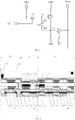
- FIG. 1 is an equivalent circuit diagram of the drive circuit, illustrating a 3T1C drive circuit. As shown in FIG. 1 , the drive circuit is electrically connected to a first gate line G1, a sensing line Sense, a power supply line VDD, a data line Data and a second gate line G2, and the drive circuit includes a switch transistor T1, a drive transistor T2, a sense transistor T3 and a storage capacitor Cst.
- a gate electrode of the switch transistor T1 is connected to the first gate line G1, the second electrode of the switch transistor T1 is connected to the data line Data, and a first electrode of the switch transistor T1 is connected to node N1.
- a gate electrode of the drive transistor T2 is connected to the node N1, a second electrode of the drive transistor T2 is connected to the power supply line VDD, and a first electrode of the drive transistor T2 is connected to node N2.
- a gate electrode of the sense transistor T3 is connected to the second gate line G2, a second electrode of the sense transistor T3 is connected to the sensing line Sense, and a first electrode of the sense transistor T3 is connected to the node N2.
- An anode of the light-emitting element OLED is connected to the node N2, and a cathode of the light-emitting element OLED is connected to the low power supply line VSS, and the light-emitting element OLED is configured to emit light with corresponding brightness in response to the current of the first electrode of the drive transistor.
- the drive circuit turns on the switch transistor T1 through the first gate line G1, a data voltage Vdata provided by the data line Data is stored in the storage capacitor Cst via the switch transistor T1, thereby controlling the drive transistor T2 to generate a current to drive the organic light-emitting diode (OLED) to emit light.
- the sense transistor T3 can extract a threshold voltage Vth and a mobility of the drive transistor T2 in response to a sensing timing, and the storage capacitor Cst is configured to maintain a voltage difference between the node N1 and the node N2 in one frame of light emission period.
- the first electrode of any of the above transistors is one of the source and drain electrodes, and the second electrode of any of the above transistors is the other of the source and drain electrodes.
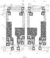
- FIG. 2A is a cross-sectional view of a display substrate according to an embodiment of the present disclosure.
- FIG. 2A is another cross-sectional view of a display substrate according to an embodiment of the present disclosure.
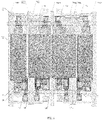
- FIG. 3 is a top view of a display substrate according to an embodiment of the present disclosure.
- an embodiment of the present disclosure provides a display substrate, including a base substrate 10 and multiple sub-pixels disposed on the base substrate 10, wherein each sub-pixel includes a light-emitting region AA and a non-light-emitting region NA, and a drive circuit is disposed in each sub-pixel.
- the drive circuit includes a storage capacitor Cst and multiple transistors, wherein the multiple transistors include a switch transistor T1, a drive transistor T2 and a sense transistor T3.
- the multiple transistors are located in the non-light-emitting region NA, the storage capacitor Cst is a transparent capacitor, and there is an overlapping region between an orthographic projection of the storage capacitor Cst on the base substrate 10 and the light-emitting region AA.
- a first electrode C1 of the storage capacitor Cst is disposed on a same layer as an active layer of the multiple transistors, but on a different layer from the source and drain electrodes of the multiple transistors.
- a second electrode C2 of the storage capacitor Cst is located on a side of the first electrode C1 close to the base substrate 10.
- a first electrode 23 of the drive transistor T2 is in direct contact with the second electrode C2 to achieve an electrical connection
- a first electrode 43 of the sense transistor T3 is in direct contact with the second electrode C2 to achieve an electrical connection.
- the first electrode 23 of the drive transistor T2 may be in direct contact with the second electrode C2 to form an electrical connection
- the first electrode 23 of the drive transistor T2 may be in electrical connection with the second electrode C2 through a light shield layer 11, depending on the connection relation between the light shield layer 11 and the second electrode C2.
- the first electrode 23 of the drive transistor T2 is in direct contact with the second electrode C2 to form an electrical connection.
- the first electrode 23 of the drive transistor T2 is in direct contact with the second electrode C2 to form an electrical connection through the light shield layer.
- the first electrode 43 of the sense transistor T3 is the same as the second electrode C2, and will not be further elaborated herein.
- the sub-pixels on the base substrate are disposed in an array. It should be noted that in FIGS. 2A to 2B and FIG. 3 one sub-pixel is taken as an example, and FIGS. 2A and 2B are cross-sectional views from different angles.
- the base substrate 10 may be a rigid substrate or a flexible substrate, wherein the rigid substrate may be, but is not limited to, one or more of glass and metal foils; and the flexible substrate may be, but is not limited to, one or more of polyethylene glycol terephthalate, ethylene terephthalate, polyether ether ketone, polystyrene, polycarbonate, polyarylate, polyarylester, polyimide, polyvinyl chloride, polyethylene, and textile fibers.
- the rigid substrate may be, but is not limited to, one or more of glass and metal foils
- the flexible substrate may be, but is not limited to, one or more of polyethylene glycol terephthalate, ethylene terephthalate, polyether ether ketone, polystyrene, polycarbonate, polyarylate, polyarylester, polyimide, polyvinyl chloride, polyethylene, and textile fibers.
- the switch transistor T1 in the embodiment of the present disclosure includes an active layer 31, a gate electrode 32, a first electrode 33 and a second electrode 34 which are disposed on a base substrate.
- the drive transistor T2 includes an active layer 21, a gate electrode 22, a first electrode 23 and a second electrode 24 which are disposed on the base substrate.
- the sense transistor T3 includes an active layer 41, a gate electrode 42, a first electrode 43, and a second electrode 44 which are disposed on the base substrate.
- the display substrate according to the embodiment of the present disclosure is a bottom emission type of OLED display substrate.
- the storage capacitor in the embodiment of the disclosure is a transparent capacitor, which does not affect the light-emitting effect of the display substrate and can ensure smooth light-emitting.
- each sub-pixel is further provided with a light-emitting element, which may be an OLED.
- the embodiments of the present disclosure provide a display substrate, including a base substrate and multiple sub-pixels disposed on the base substrate, wherein each sub-pixel includes a light-emitting region and a non-light-emitting region, and each sub-pixel is provided with a drive circuit; the drive circuit includes a storage capacitor and multiple transistors; the multiple transistors include a switch transistor, a drive transistor and a sense transistor. For each sub-pixel, the multiple transistors are located in the non-light-emitting region, the storage capacitor is a transparent capacitor, and there is an overlapping region between the orthographic projection of the storage capacitor on the base substrate and the light-emitting region.
- a first electrode of the storage capacitor is disposed in a same layer as an active layer of the multiple transistors and in a different layer from the source and drain electrodes of the multiple transistors, and a second electrode of the storage capacitor is located on a side of the first electrode close to the base substrate.
- a first electrode of the drive transistor is in direct contact with the second electrode, and a first electrode of the sense transistor is in direct contact with the second electrode.
- the present disclosure can greatly reduce an area ratio of the storage capacitor in the non-emitting region while ensuring an aperture ration by providing an overlapping region between the orthographic projection of the transparent storage capacitor on the base substrate and the light-emitting region, so that the area occupied by each sub-pixel can be reduced and a high PPI of the display substrate can be achieved.
- each transistor there is an overlapping region between an orthographic projection of the active layer of the transistor on the substrate and an orthographic projection of the gate electrode of the transistor on the substrate.
- a display substrate according to an embodiment of the present disclosure further includes a light shield layer 11 and a buffer layer 12 disposed on a side of the active layer of the transistor close to the base substrate 10, and the light shield layer 11 and the second electrode C2 are disposed on a side of the buffer layer 12 close to the base substrate 10.
- an orthographic projection of the second electrode C2 on the base substrate 10 covers an orthographic projection of the light shield layer 11 on the base substrate 10, and a surface of the light shield layer 11 close to the second electrode C2 is completely in contact with the second electrode C2.
- the light shield layer 11 is disposed on the side of the second electrode C2 close to the base substrate 10, or the second electrode C2 is disposed on the side of the light shield layer 11 close to the base substrate 10, wherein FIGS. 2A to 2B and FIG. 3 all take the light shield layer 11 disposed on the side of the second electrode C2 close to the base substrate 10 as an example.
- the first electrode 23 of the drive transistor T2 is electrically connected to the second electrode C2 through the conductive light shield layer 11
- the first electrode 43 of the sense transistor T3 is electrically connected to the second electrode C2 through the light shield layer 11.
- the surface of the light shield layer 11 close to the second electrode C2 is in complete contact with the second electrode C2, avoiding arrangement of an insulating layer between the light shield layer and the second electrode, which not only reduces the number of layers and the thickness of the display substrate, but also reduces the number of use of masks, simplifies the preparation process and reduces manufacturing costs of the display substrate.
- the orthographic projection of the light shield layer 11 on the base substrate 10 covers an orthographic projection of a channel region A1 of the active layer 21 of the drive transistor T2 on the base substrate 10.
- the light shield layer 11 is made of metal, such as silver, aluminum and the like, which is not limited by the embodiments of the disclosure.
- a display substrate according to an embodiment of the present disclosure further includes an interlayer insulating layer 14 disposed between the source and drain electrodes of the transistor and an active layer of the transistor.
- the buffer layer 12 in the display substrate includes a first via hole V1 and a second via hole V2 which expose the second electrode
- the interlayer insulating layer 14 includes a third via hole V3 exposing the first via hole V1 and a fourth via hole V4 exposing the second via hole V2.
- the first electrode 23 of the drive transistor T2 is connected to the second electrode C2 through the first via hole V1 and the third via hole V3, and the first electrode 43 of the sense transistor T3 is connected to the second electrode C2 through the second via hole V2 and the fourth via hole V4.
- the interlayer insulating layer 14 is further provided with via holes exposing the active layers of the multiple transistors, and the source and drain electrodes of the multiple transistors are connected to the active layers through the via holes.
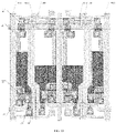
- FIG. 4 is another top view of a display substrate according to an embodiment of the present disclosure.
- the display substrate according to the embodiment of the present disclosure further includes multiple rows of gate lines and multiple columns of data lines disposed on the base substrate, wherein each sub-pixel is defined by intersection of gate lines and data lines, and the gate lines includes a first gate line G1 and a second gate line G2.
- FIG. 4 takes four sub-pixels as an example.
- FIG. 2A is a cross-sectional view of FIG. 4 along A-A direction
- FIG. 2B is a cross-sectional view of FIG. 4 along B-B direction.
- a first gate line G1 and a second gate line G2 are disposed in a same layer as the gate electrodes of the transistors and the data lines Data are disposed in a same layer as the source and drain electrodes of the transistors.
- the first electrode C1 is respectively connected to the first electrode 33 of the switch transistor T1 and the gate electrode 22 of the drive transistor T2.
- the second electrode C2 is respectively connected to the first electrode 23 of the drive transistor T2 and the first electrode 43 of the sense transistor T3.
- the gate electrode of the switch transistor T1 is connected to the first gate line G1 among the gate lines corresponding to the sub-pixel.
- the second electrode 34 of the switch transistor T1 is connected to the data line Data corresponding to the sub-pixel, and the gate electrode of the sense transistor T3 is connected to the second gate line G2 among the gate lines corresponding to the sub-pixel.
- the light-emitting region AA includes a first side and a second side which are oppositely disposed along an extending direction of the data line Data.
- the sense transistor T3 and the second gate line G2 are both located on the first side of the light-emitting region AA, and the switch transistor T1, the drive transistor T2 and the first gate line G1 are all located on the second side of the light-emitting region AA.
- the display substrate further includes power supply lines VDD and a sensing line Sense which are disposed in a same layer as the data lines Data.
- Each pixel includes four sub-pixels disposed along an extending direction of the gate line, and each pixel corresponds to two columns of power supply lines and one column of sensing line.
- the pixel structures of a second sub-pixel and a third sub-pixel are symmetrically disposed, and a first sub-pixel and a fourth sub-pixel are symmetrically disposed.
- the sensing line Sense corresponding to the pixel is located between the second sub-pixel P2 and the third sub-pixel P3, one column of power supply line VDD corresponding to the pixel is located on a side of the first sub-pixel P1 away from the second sub-pixel P2, and another column of power supply line VDD corresponding to the pixel is located on a side of the fourth sub-pixel P4 away from the third sub-pixel P3.
- a data line Data corresponding to the first sub-pixel P1 is located on a side of the first sub-pixel P1 close to the second sub-pixel P2.
- a data line corresponding to the second sub-pixel P2 is located on a side of the second sub-pixel P2 close to the first sub-pixel P1.
- a data line corresponding to the third sub-pixel P3 is located on a side of the third sub-pixel P3 close to the fourth sub-pixel P4.
- a data line corresponding to the fourth sub-pixel P4 is located on a side of the fourth sub-pixel P4 close to the third sub-pixel P3.
- the display substrate according to an embodiment of the present disclosure further includes: power connection lines VL disposed in a same layer as the gate electrodes of the transistors and sensing connection lines SL disposed in a same layer as the light shield layer 11.
- Each pixel corresponds to two power connection lines disposed along the extending direction of the gate lines and two sensing connection lines SL disposed along the extending direction of the gate lines.
- the power connection lines VL respectively correspond to the power supply lines VDD, and each power connection line is connected to a corresponding power supply line.
- the two sensing connection lines SL are connected to the sensing lines Sense.
- a second electrode of the drive transistor of the second sub-pixel P2 is connected to one power connection line VL, and a second electrode of the drive transistor of the third sub-pixel P3 is connected to another power connection line VL.
- a second electrode of the sense transistor of the first sub-pixel P1 is connected to one sensing connection line SL, and a second electrode of the sense transistor of the fourth sub-pixel P4 is connected to another sensing connection line SL.
- the sensing connection lines SL may have a single-layer structure or a double-layer structure.
- a sensing connection line SL When a sensing connection line SL has a single-layer structure, it is disposed in a same layer as the light shield layer or the second electrode, and when the sensing connection line SL has a double-layer structure, the first layer and the light shield layer of the sensing connection line are disposed in a same layer, while the second layer and the second electrode are disposed in the same layer.
- the sensing connection lines and the light shield layer are disposed in a same layer as an example.
- a display substrate according to an embodiment of the present disclosure further includes a gate insulating layer 13 disposed between a gate electrode of a transistor and an active layer of the transistor.
- An orthographic projection of the gate insulating layer 13 on the base substrate 10 coincides with an orthographic projection of the gate electrode of the transistor on the base substrate 10.
- the buffer layer 12, the gate insulating layer 13, and the interlayer insulating layer 14 are made of silicon oxide, silicon nitride or a composite of silicon oxide and silicon nitride, which is not limited by the embodiments of the present disclosure.
- the buffer layer 12 is further provided with a fifth via hole V5, wherein the fifth via hole V5 exposes the sensing connection line SL.
- the interlayer insulating layer 14 is further provided with a sixth via hole V6 exposing the fifth via hole V5, wherein the second electrode 44 of the sense transistor T3 is connected to the sensing connection line SL through the fifth via hole V5 and the sixth via hole V6.
- the first electrode C1 is made of transparent metal oxide, and the transparent metal oxide includes indium gallium zinc oxide (IGZO) or the like, which is not limited by the embodiments of the disclosure.
- IGZO indium gallium zinc oxide
- the second electrode C2 is made of a transparent conductive material, and the transparent conductive material includes indium tin oxides (ITO), zinc tin oxide or the like, which is not limited by the embodiments of the disclosure.
- ITO indium tin oxides
- zinc tin oxide or the like, which is not limited by the embodiments of the disclosure.
- FIG. 5 is another top view of a display substrate according to an embodiment of the present disclosure
- FIG. 6 is another top view of a display substrate according to an embodiment of the present disclosure.
- each sub-pixel is also provided with a light-emitting element and a filter 50 of the same color as the sub-pixel.
- the light-emitting element includes an anode 61, an organic light-emitting layer 62 and a cathode 63 which are sequentially disposed, wherein the anode 61 is connected to the first electrode 43 of the sense transistor T3, the anode 61 is a transmission electrode and the cathode 63 is a reflection electrode.
- the anode 61 may be made of a transparent conductive material, such as indium tin oxide ITO, zinc tin oxide or the like, which is not limited by the embodiments of the present disclosure.
- the cathode 63 is made of metal, such as silver, aluminum or the like, which is not limited by the embodiments of the disclosure.
- An orthographic projection of the anode 61 on the base substrate 10 covers an orthographic projection of the filter 50 on the base substrate 10.
- a display substrate further includes a passivation layer 15 disposed on a side of the source and drain electrodes of the transistor away from the base substrate 10, a planarization layer 16 disposed between the anode 61 and the filter 50, and a pixel defining layer 17 for defining a sub-pixel region, wherein the pixel defining layer 17 is disposed on a side of the planarization layer 16 away from the base substrate 10.
- the passivation layer 15 is disposed on a side of the filter 50 close to the base substrate 10, and the planarization layer 16 is disposed between the light-emitting element and the filter 50.
- the passivation layer 15 is provided with a seventh via hole V7 exposing the first electrode 43 of the sense transistor T3, and the planarization layer 16 is provided with an eighth via hole V8 exposing the seventh via hole V7.
- the anode 61 is connected to the first electrode 43 of the sense transistor T3 through the seventh via hole V7 and the eighth via hole V8.
- An orthographic projection of the eighth via hole V8 on the base substrate 10 does not completely coincide with an orthographic projection of the fourth via hole V4 on the base substrate 10.
- a display substrate according to an embodiment of the present disclosure further includes a supporting part 70 disposed on a side of the light-emitting element away from the base substrate 10 and includes a cover plate 80 disposed on a side of the supporting part 70 away from the base substrate 10.
- the cover plate 80 is configured to protect the light-emitting element.
- the cover plate 80 may be a glass cover plate.
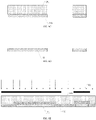
- FIG. 7 is a flowchart of a method for preparing a display substrate according to an embodiment of the present disclosure. As shown in FIG. 7, the method for preparing a display substrate according to an embodiment of the present disclosure includes the following steps:
- the sub-pixels are disposed on the base substrate in an array.
- FIGS. 2A to 2B take one sub-pixel as an example.
- each sub-pixel includes a light-emitting region and a non-light-emitting region, and each sub-pixel is provided therein with a drive circuit.
- the drive circuit includes a storage capacitor and multiple transistors, wherein the multiple transistors include a switch transistor, a drive transistor and a sense transistor.
- the multiple transistors are located in the non-light-emitting region, the storage capacitor is a transparent capacitor, and there is an overlapping region between an orthographic projection of the storage capacitor on the base substrate and the light-emitting region.
- a first electrode of the storage capacitor is disposed in a same layer as an active layer of the multiple transistors, and a second electrode of the storage capacitor is located on a side of the first electrode close to the base substrate.
- a first electrode of the drive transistor is in direct contact with the second electrode, and a first electrode of the sense transistor is in direct contact with the second electrode.
- the display substrate is a display substrate provided in the preceding embodiments, and has a similar implementation principle and implementation effects, which will not be described further here.
- the display substrate further includes gate lines, data lines, power supply lines and sensing lines, wherein the gate lines includes a first gate line and a second gate line.
- Step S2 specifically includes: forming a light shield layer and a second electrode on the base substrate; forming a first electrode and active layers of multiple transistors on the light shield layer and the second electrode; forming gate electrodes of the multiple transistors, first gate line and second gate line on the first electrode and the active layers of the multiple transistors; forming data lines, power supply lines, sensing lines and source and drain electrodes of the multiple transistors on the first electrode and the active layers of the multiple transistors; and sequentially forming filters and light-emitting elements on the data lines, the power supply lines, the sensing lines and the source and drain electrodes of the multiple transistors.
- forming a light shield layer and a second electrode on the base substrate includes sequentially forming the light shield layer and the second electrode on the base substrate, or sequentially forming the second electrode and the light shield layer on the base substrate, or simultaneously forming the second electrode and the light shield layer on the base substrate.
- sequentially forming the light shield layer and the second electrode on the base substrate includes forming the light shield layer on the base substrate using a first mask and forming the second electrode on the light shield layer using a second mask.
- sequentially forming the second electrode and the light shield layer on the base substrate includes forming the second electrode on the base substrate by a patterning process using a second mask and forming the light shield layer on the second electrode using a first mask.
- simultaneously forming the second electrode and the light shield layer on the base substrate includes sequentially depositing a light shielding thin film and a transparent conductive thin film on the base substrate, and simultaneously forming the second electrode and the light shield layer by using a halftone mask.
- the patterning process herein includes: photoresist coating, exposure, development, etching, and photoresist stripping, etc.
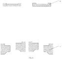
- FIGS. 8A to 8H Taking the light shield layer on the side of the second electrode close to the base substrate as an example, a preparation process of the light shield layer and the second electrode will be further explained with reference to FIGS. 8A to 8H , which includes the following steps:
- the steps of forming a first electrode and active layers of the multiple transistors on the light shield layer and the second electrode; forming gate electrodes of the multiple transistors, first gate line and second gate line on the first electrode and the active layers of the multiple transistors; forming the data lines, the power supply lines, the sensing lines and the source and drain electrodes of the multiple transistors on the gate electrodes of the transistors, the first gate line and the second gate line include forming a buffer layer including a first via hole, a second via hole and a fifth via hole on the light shield layer and the second electrode through a patterning process; forming the first electrode and the active layers of the multiple transistors on the buffer layer by using the same process; forming the gate electrodes of the multiple transistors, the first gate line and the second gate line on the first electrode and the active layers of the multiple transistors includes forming an interlayer insulating layer including a third via hole, a fourth via hole and a sixth via hole on the gate electrodes, the first gate line and the second
- the first and second via holes expose the second electrode
- the fifth via hole exposes the sensing connection line
- the third via hole exposes the first via hole
- the fourth via hole exposes the second via hole
- the sixth via hole exposes the fifth via hole.
- the steps of forming the first electrode and the active layers of the multiple transistors on the light shield layer and the second electrode; forming the gate electrodes of the transistors, the first gate line and the second gate line on the first electrode and the active layers of the transistors; forming the data lines, the power supply lines, the sensing lines and the source and drain electrodes of the multiple transistors on the gate electrodes of the multiple transistors, the first gate line and the second gate line include forming a first insulating thin film on the light shield layer and the second electrode; forming the first electrode and the active layers of the multiple transistors on the first insulating thin film by using the same process; forming the gate electrodes of the multiple transistors, the first gate line and the second gate line on the first electrode and the active layers of the multiple transistors; forming a second insulating thin film on the gate electrodes of the transistor, the first gate line and the second gate line; and processing the first insulating thin film and the second insulating thin film through a patterning process to form a buffer layer
- Sequentially forming filters and light-emitting elements on the data lines, the power supply lines, the sensing lines and the source and drain electrodes of the multiple transistors includes forming a passivation layer including a seventh via hole on the data lines, the power supply lines, the sensing lines and the source and drain electrodes of the multiple transistors, wherein the seventh via hole exposes the first electrode of the sense transistor; sequentially forming the filters and a planarization layer including an eighth via hole on the passivation layer, wherein the eighth via hole exposes the seventh via hole; and forming the light-emitting elements on the planarization layer.
- the above embodiments can simplify the preparation processes of the display substrate.
- the sensing connection lines has a single-layer structure and are disposed in a same layer as the light shield layer, and the light shield layer is disposed on the side of the second electrode close to the base substrate
- the method for preparing the display substrate according to the embodiments of the present disclosure will be further explained with reference to FIGS. 9 to 15 , and the method includes the following steps:
- an embodiment of the present disclosure further provides a display apparatus, including a display substrate.
- the display apparatus may be any product or component with a display function such as a mobile phone, a tablet computer, a television, a display, a laptop computer, a digital photo frame, a navigator, etc.
- a display function such as a mobile phone, a tablet computer, a television, a display, a laptop computer, a digital photo frame, a navigator, etc.
- Other essential components of the display apparatus is well known to those of ordinary skills in the art, which will not be described in detail here, and should not be construed as a limitation on the present disclosure.
- the implementation of the display apparatus may refer to the embodiment of the embedded touch screen described above, and the repetition will not be described in detail here.
- the display substrate is the display substrate provided in any of the preceding embodiments, and has an identical or similar implementation principle and implementation effects, which will not be described further here.
Landscapes
- Engineering & Computer Science (AREA)
- Microelectronics & Electronic Packaging (AREA)
- Physics & Mathematics (AREA)
- Geometry (AREA)
- Power Engineering (AREA)
- General Physics & Mathematics (AREA)
- Computer Hardware Design (AREA)
- Condensed Matter Physics & Semiconductors (AREA)
- General Engineering & Computer Science (AREA)
- Manufacturing & Machinery (AREA)
- Devices For Indicating Variable Information By Combining Individual Elements (AREA)
- Electroluminescent Light Sources (AREA)
- Thin Film Transistor (AREA)
Applications Claiming Priority (2)
| Application Number | Priority Date | Filing Date | Title |
|---|---|---|---|
| CN201911038401.5A CN112750859B (zh) | 2019-10-29 | 2019-10-29 | 一种显示基板及其制作方法、显示装置 |
| PCT/CN2020/124452 WO2021083226A1 (fr) | 2019-10-29 | 2020-10-28 | Substrat d'affichage ainsi que procédé de fabrication associé, et dispositif d'affichage |
Publications (2)
| Publication Number | Publication Date |
|---|---|
| EP4053905A1 true EP4053905A1 (fr) | 2022-09-07 |
| EP4053905A4 EP4053905A4 (fr) | 2022-12-21 |
Family
ID=75641855
Family Applications (1)
| Application Number | Title | Priority Date | Filing Date |
|---|---|---|---|
| EP20878024.7A Pending EP4053905A4 (fr) | 2019-10-29 | 2020-10-28 | Substrat d'affichage ainsi que procédé de fabrication associé, et dispositif d'affichage |
Country Status (6)
| Country | Link |
|---|---|
| US (1) | US20220102460A1 (fr) |
| EP (1) | EP4053905A4 (fr) |
| JP (1) | JP2023501023A (fr) |
| KR (1) | KR20220088634A (fr) |
| CN (1) | CN112750859B (fr) |
| WO (1) | WO2021083226A1 (fr) |
Families Citing this family (4)
| Publication number | Priority date | Publication date | Assignee | Title |
|---|---|---|---|---|
| CN112750861A (zh) * | 2019-10-29 | 2021-05-04 | 京东方科技集团股份有限公司 | 一种显示基板及其制作方法、显示装置 |
| CN113594220B (zh) * | 2021-07-30 | 2024-05-14 | 京东方科技集团股份有限公司 | 显示基板及其测试方法、制备方法、显示装置 |
| CN114203631A (zh) * | 2021-12-10 | 2022-03-18 | Tcl华星光电技术有限公司 | 显示面板的制造方法以及显示面板 |
| CN115274712A (zh) * | 2022-08-15 | 2022-11-01 | 京东方科技集团股份有限公司 | 显示背板及其制备方法、显示装置 |
Family Cites Families (13)
| Publication number | Priority date | Publication date | Assignee | Title |
|---|---|---|---|---|
| JPH08184852A (ja) * | 1994-12-27 | 1996-07-16 | Sharp Corp | アクティブマトリクス型表示装置 |
| CN103904086B (zh) * | 2012-12-24 | 2017-10-27 | 上海天马微电子有限公司 | 一种薄膜晶体管阵列基板 |
| KR102139355B1 (ko) * | 2013-12-31 | 2020-07-29 | 엘지디스플레이 주식회사 | 유기전계발광표시장치 및 그 제조방법 |
| KR101849590B1 (ko) * | 2016-10-31 | 2018-05-31 | 엘지디스플레이 주식회사 | 유기 발광 표시 장치 및 그 제조 방법 |
| KR102546985B1 (ko) * | 2016-11-21 | 2023-06-27 | 엘지디스플레이 주식회사 | 대면적 초고해상도 평판 표시장치 |
| KR102662278B1 (ko) * | 2016-11-30 | 2024-05-02 | 엘지디스플레이 주식회사 | 유기 발광 표시 장치 및 그 제조 방법 |
| KR102431929B1 (ko) * | 2017-10-31 | 2022-08-12 | 엘지디스플레이 주식회사 | 표시장치 및 그 제조방법 |
| KR102670405B1 (ko) * | 2018-05-09 | 2024-05-30 | 엘지디스플레이 주식회사 | 전계발광표시장치 |
| KR102571354B1 (ko) * | 2018-05-16 | 2023-08-28 | 엘지디스플레이 주식회사 | 전계발광 표시장치 |
| CN109273498B (zh) * | 2018-09-25 | 2021-01-26 | 京东方科技集团股份有限公司 | 一种阵列基板及其制备方法、显示面板、显示装置 |
| KR102542808B1 (ko) * | 2018-10-15 | 2023-06-12 | 엘지디스플레이 주식회사 | 표시장치 |
| CN110112183A (zh) * | 2019-04-12 | 2019-08-09 | 深圳市华星光电半导体显示技术有限公司 | 双面显示面板及其制备方法 |
| CN110071069B (zh) * | 2019-04-19 | 2021-11-23 | 深圳市华星光电半导体显示技术有限公司 | 显示背板及其制作方法 |
-
2019
- 2019-10-29 CN CN201911038401.5A patent/CN112750859B/zh active Active
-
2020
- 2020-10-28 WO PCT/CN2020/124452 patent/WO2021083226A1/fr unknown
- 2020-10-28 EP EP20878024.7A patent/EP4053905A4/fr active Pending
- 2020-10-28 JP JP2021564799A patent/JP2023501023A/ja active Pending
- 2020-10-28 KR KR1020217035675A patent/KR20220088634A/ko unknown
- 2020-10-28 US US17/298,032 patent/US20220102460A1/en active Pending
Also Published As
| Publication number | Publication date |
|---|---|
| WO2021083226A1 (fr) | 2021-05-06 |
| EP4053905A4 (fr) | 2022-12-21 |
| JP2023501023A (ja) | 2023-01-18 |
| WO2021083226A9 (fr) | 2022-05-19 |
| KR20220088634A (ko) | 2022-06-28 |
| CN112750859B (zh) | 2022-07-29 |
| US20220102460A1 (en) | 2022-03-31 |
| CN112750859A (zh) | 2021-05-04 |
Similar Documents
| Publication | Publication Date | Title |
|---|---|---|
| EP4053904A1 (fr) | Substrat d'affichage et son procédé de fabrication, et dispositif d'affichage | |
| CN112071882B (zh) | 显示基板及其制备方法、显示装置 | |
| US20220376024A1 (en) | Display Substrate and Manufacturing Method Therefor, and Display Apparatus | |
| EP4053905A1 (fr) | Substrat d'affichage ainsi que procédé de fabrication associé, et dispositif d'affichage | |
| KR102443121B1 (ko) | 디스플레이 패널 및 그 제조 방법 및 디스플레이 디바이스 | |
| US11758780B2 (en) | Display substrate and display apparatus | |
| US20240153461A1 (en) | Display Apparatus with Compensation and Driving Method therefor | |
| US20220123073A1 (en) | Display Substrate and Preparation Method thereof, and Display Apparatus | |
| CN113196494B (zh) | 显示基板及其制备方法、显示装置 | |
| US11721291B2 (en) | Display substrate and display apparatus | |
| CN115769296A (zh) | 显示基板及其制备方法、显示装置 | |
| CN115715121A (zh) | 显示面板及其制备方法、显示装置 | |
| CN113314071B (zh) | 显示基板及显示装置 | |
| US20230026444A1 (en) | Display device and driving method therefor | |
| US20240172476A1 (en) | Display Substrate and Display Apparatus | |
| EP4336987A1 (fr) | Substrat d'affichage et son procédé de fabrication, et dispositif d'affichage | |
| US20240164156A1 (en) | Display Substrate, Preparation Method thereof, and Display Apparatus | |
| US20240212602A1 (en) | Display Substrate and Preparation Method thereof, and Display Apparatus | |
| US20240161691A1 (en) | Display Substrate and Display Apparatus | |
| US20240306442A1 (en) | Display Substrate and Preparation Method therefor, and Display Apparatus | |
| US20230359300A1 (en) | Touch Display Substrate, Manufacturing Method Therefor, and Touch Display Device | |
| US20230180521A1 (en) | Display Substrate, Preparation Method thereof, and Display Apparatus | |
| CN115529844A (zh) | 显示基板及其制备方法、显示装置 | |
| KR20210101346A (ko) | 표시 장치 및 표시 장치의 제조 방법 |
Legal Events
| Date | Code | Title | Description |
|---|---|---|---|
| STAA | Information on the status of an ep patent application or granted ep patent |
Free format text: STATUS: UNKNOWN |
|
| STAA | Information on the status of an ep patent application or granted ep patent |
Free format text: STATUS: THE INTERNATIONAL PUBLICATION HAS BEEN MADE |
|
| PUAI | Public reference made under article 153(3) epc to a published international application that has entered the european phase |
Free format text: ORIGINAL CODE: 0009012 |
|
| STAA | Information on the status of an ep patent application or granted ep patent |
Free format text: STATUS: REQUEST FOR EXAMINATION WAS MADE |
|
| 17P | Request for examination filed |
Effective date: 20210426 |
|
| AK | Designated contracting states |
Kind code of ref document: A1 Designated state(s): AL AT BE BG CH CY CZ DE DK EE ES FI FR GB GR HR HU IE IS IT LI LT LU LV MC MK MT NL NO PL PT RO RS SE SI SK SM TR |
|
| A4 | Supplementary search report drawn up and despatched |
Effective date: 20221123 |
|
| RIC1 | Information provided on ipc code assigned before grant |
Ipc: H01L 21/77 20170101ALI20221117BHEP Ipc: H01L 27/32 20060101AFI20221117BHEP |
|
| DAV | Request for validation of the european patent (deleted) | ||
| DAX | Request for extension of the european patent (deleted) |