EP4052020B1 - Optisches abbildungssystem - Google Patents
Optisches abbildungssystem Download PDFInfo
- Publication number
- EP4052020B1 EP4052020B1 EP20800589.2A EP20800589A EP4052020B1 EP 4052020 B1 EP4052020 B1 EP 4052020B1 EP 20800589 A EP20800589 A EP 20800589A EP 4052020 B1 EP4052020 B1 EP 4052020B1
- Authority
- EP
- European Patent Office
- Prior art keywords
- light
- optical
- sample
- excitation
- substrate
- Prior art date
- Legal status (The legal status is an assumption and is not a legal conclusion. Google has not performed a legal analysis and makes no representation as to the accuracy of the status listed.)
- Active
Links
Images


Classifications
-
- G—PHYSICS
- G02—OPTICS
- G02B—OPTICAL ELEMENTS, SYSTEMS OR APPARATUS
- G02B21/00—Microscopes
- G02B21/0004—Microscopes specially adapted for specific applications
- G02B21/002—Scanning microscopes
- G02B21/0024—Confocal scanning microscopes (CSOMs) or confocal "macroscopes"; Accessories which are not restricted to use with CSOMs, e.g. sample holders
- G02B21/0052—Optical details of the image generation
- G02B21/0056—Optical details of the image generation based on optical coherence, e.g. phase-contrast arrangements, interference arrangements
-
- G—PHYSICS
- G01—MEASURING; TESTING
- G01N—INVESTIGATING OR ANALYSING MATERIALS BY DETERMINING THEIR CHEMICAL OR PHYSICAL PROPERTIES
- G01N21/00—Investigating or analysing materials by the use of optical means, i.e. using sub-millimetre waves, infrared, visible or ultraviolet light
- G01N21/17—Systems in which incident light is modified in accordance with the properties of the material investigated
- G01N21/41—Refractivity; Phase-affecting properties, e.g. optical path length
- G01N21/45—Refractivity; Phase-affecting properties, e.g. optical path length using interferometric methods; using Schlieren methods
-
- A—HUMAN NECESSITIES
- A61—MEDICAL OR VETERINARY SCIENCE; HYGIENE
- A61B—DIAGNOSIS; SURGERY; IDENTIFICATION
- A61B5/00—Measuring for diagnostic purposes; Identification of persons
- A61B5/0059—Measuring for diagnostic purposes; Identification of persons using light, e.g. diagnosis by transillumination, diascopy, fluorescence
-
- G—PHYSICS
- G01—MEASURING; TESTING
- G01N—INVESTIGATING OR ANALYSING MATERIALS BY DETERMINING THEIR CHEMICAL OR PHYSICAL PROPERTIES
- G01N21/00—Investigating or analysing materials by the use of optical means, i.e. using sub-millimetre waves, infrared, visible or ultraviolet light
- G01N21/62—Systems in which the material investigated is excited whereby it emits light or causes a change in wavelength of the incident light
- G01N21/63—Systems in which the material investigated is excited whereby it emits light or causes a change in wavelength of the incident light optically excited
- G01N21/64—Fluorescence; Phosphorescence
- G01N21/645—Specially adapted constructive features of fluorimeters
- G01N21/6456—Spatial resolved fluorescence measurements; Imaging
- G01N21/6458—Fluorescence microscopy
-
- G—PHYSICS
- G02—OPTICS
- G02B—OPTICAL ELEMENTS, SYSTEMS OR APPARATUS
- G02B21/00—Microscopes
- G02B21/0004—Microscopes specially adapted for specific applications
- G02B21/0088—Inverse microscopes
-
- G—PHYSICS
- G02—OPTICS
- G02B—OPTICAL ELEMENTS, SYSTEMS OR APPARATUS
- G02B21/00—Microscopes
- G02B21/0004—Microscopes specially adapted for specific applications
- G02B21/0092—Polarisation microscopes
-
- G—PHYSICS
- G02—OPTICS
- G02B—OPTICAL ELEMENTS, SYSTEMS OR APPARATUS
- G02B21/00—Microscopes
- G02B21/06—Means for illuminating specimens
- G02B21/08—Condensers
- G02B21/14—Condensers affording illumination for phase-contrast observation
-
- G—PHYSICS
- G02—OPTICS
- G02B—OPTICAL ELEMENTS, SYSTEMS OR APPARATUS
- G02B21/00—Microscopes
- G02B21/16—Microscopes adapted for ultraviolet illumination ; Fluorescence microscopes
-
- G—PHYSICS
- G01—MEASURING; TESTING
- G01N—INVESTIGATING OR ANALYSING MATERIALS BY DETERMINING THEIR CHEMICAL OR PHYSICAL PROPERTIES
- G01N21/00—Investigating or analysing materials by the use of optical means, i.e. using sub-millimetre waves, infrared, visible or ultraviolet light
- G01N21/62—Systems in which the material investigated is excited whereby it emits light or causes a change in wavelength of the incident light
- G01N21/63—Systems in which the material investigated is excited whereby it emits light or causes a change in wavelength of the incident light optically excited
- G01N21/64—Fluorescence; Phosphorescence
- G01N2021/6417—Spectrofluorimetric devices
- G01N2021/6419—Excitation at two or more wavelengths
-
- G—PHYSICS
- G01—MEASURING; TESTING
- G01N—INVESTIGATING OR ANALYSING MATERIALS BY DETERMINING THEIR CHEMICAL OR PHYSICAL PROPERTIES
- G01N21/00—Investigating or analysing materials by the use of optical means, i.e. using sub-millimetre waves, infrared, visible or ultraviolet light
- G01N21/62—Systems in which the material investigated is excited whereby it emits light or causes a change in wavelength of the incident light
- G01N21/63—Systems in which the material investigated is excited whereby it emits light or causes a change in wavelength of the incident light optically excited
- G01N21/64—Fluorescence; Phosphorescence
- G01N21/6428—Measuring fluorescence of fluorescent products of reactions or of fluorochrome labelled reactive substances, e.g. measuring quenching effects, using measuring "optrodes"
- G01N2021/6439—Measuring fluorescence of fluorescent products of reactions or of fluorochrome labelled reactive substances, e.g. measuring quenching effects, using measuring "optrodes" with indicators, stains, dyes, tags, labels, marks
- G01N2021/6441—Measuring fluorescence of fluorescent products of reactions or of fluorochrome labelled reactive substances, e.g. measuring quenching effects, using measuring "optrodes" with indicators, stains, dyes, tags, labels, marks with two or more labels
Definitions
- This specification relates to optical imaging.
- the Interferometric Scattering Microscopy is an optical technique that enables label-free imaging of individual macromolecules and nanoparticles.
- An iSCAT microscope can detect unlabelled single molecules in solution with an optical signal strength that is a characteristic for the mass of the detected particles.
- Such optical mass spectroscopy of individual molecules may be well-suited for studying a wide range of molecular assembly processes including protein-protein interactions and thus has potential applications in fields such as medical diagnosis and drug development.
- the iSCAT may be used for biosensing i.e. for detection and quantification of bio-markers in a sample.
- iSCAT enables the detection of surface binding events with high sensitivity and enables new label-free biochemical assays based on highly functionalised surfaces and specific binding.
- interferometric scattering microscopy is capable of detecting and weighing unlabeled, single molecules and facilitates the study of molecular assembly properties
- the scope of applications may be expanded by combining iSCAT with super-resolution, single molecule fluorescence microscopy.
- Cole et al. Label-Free Single-Molecule Imaging with numerical-Aperture-Shaped Interferometric Scattering Microscopy", ACS Photonics 2017, 4, 211-216 , discloses interferometric scattering as method for interrogating nanoscale objects.
- an optical system for optically imaging a sample including a nanoscale object.
- the optical system comprises an imaging lens, an illumination source configured to provide an excitation light, a detector and a substrate for supporting the sample.
- a sample interface arranged to reflect the excitation light, is formed between the sample and a first side of the substrate facing the sample when the sample is applied on the substrate.
- the optical imaging system is arranged such that the excitation light is sent into the substrate via the imaging lens and such that the detector receives a reference light and a scattered light.
- the reference light comprises a part of the excitation light reflected at the sample interface and collected by the imaging lens and the scattered light comprises a part of the excitation light scattered by the nanoscale object and collected by the imaging lens.
- the optical system is configured such that the nanoscale object is imaged at the detector, in response to the excitation light, by an optical contrast of an interference pattern between the reference light and the scattered light.
- the substrate comprises an optical coating disposed on the first side of the substrate such that the sample is in contact with the optical coating when the sample is applied on the substrate. A degree of reflection of the excitation light at the sample interface is such that the optical contrast is larger compared to the optical contrast obtained with the sample interface formed without the optical coating.
- the optical system comprises further a first optical element configured to be a polarising beam splitter and configured to separate a path for the excitation light into the imaging lens and a path for the reference light and the scattered light into the detector, and a structured waveplate between the first optical element and the imaging lens, wherein the structured waveplate comprises an inner region configured to impart a first retardation to the excitation light and an outer region configured to impart a second retardation to the excitation light.
- a difference between the first retardation and the second retardation is between 0.7 ⁇ and 0.99 ⁇ .
- the second retardation is zero.
- an area of the inner region is less than 4mm 2 .
- the optical system further comprises a quarter wave plate between the first optical element and the imaging lens.
- the excitation light is s-polarised with respect to an alignment of the polarising beam splitter such that the excitation light is substantially reflected at the first optical element into the imaging lens.
- the illumination source comprises a first illumination source and a second illumination source.
- the first illumination source provides a first excitation light at a wavelength within a first wavelength band, the first excitation light being the excitation light for the reference light and the scattered light.
- the second illumination source provides a second excitation light at a wavelength within a second wavelength band for a fluorescence excitation of the nanoscale object.
- the first optical element is further configured to combine the second excitation light with the first excitation light into the imaging lens and to transmit a fluorescence light into the detector such that the nanoscale object is further imaged at the detector by the fluorescence light emitted by the nanoscale object.
- the nanoscale object comprises a plurality of groups of fluorophores, each group having a different excitation spectrum.
- the second illumination source is configured to provide the second excitation light at a plurality of wavelengths for fluorescence excitation of the respective groups.
- the first illumination source comprises a superluminescence light emitting diode or a single mode diode laser with a fast current modulation.
- the optical system is configured such that the interference pattern and the fluorescence light are received simultaneously on separate parts of a light-sensitive area of the detector.
- an angle of incidence of the excitation light is arranged such that a degree of spurious reflection of the excitation light into the detector is reduced.
- the optical coating is configured such that the degree of reflection of the excitation light at the sample interface matches a degree of spurious reflection of the excitation light.
- the spurious reflection corresponds to part the excitation light which is reflected at the interfaces formed within the optical system other than the sample interface and subsequently arrives at the detector.
- the optical coating is configured such that the degree of reflection of the excitation light at the sample interface is higher than a degree of spurious reflection of the excitation light at the interfaces formed within the optical system other than the sample interface and lower than the degree of reflection of the excitation light at the sample interface formed without the optical coating.
- the optical coating includes an intermediate layer on the first side of the substrate and an external layer on the intermediate layer, arranged to receive the sample when the sample is applied on the substrate.
- the intermediate layer comprises one or more of aluminium oxide, Al 2 O 3 , hafnium dioxide, HfO 2 , tantalum pentoxide, Ta 2 O 5 , niobium pentoxide, Nb 2 O 5 , titanium dioxide, TiO 2 , and silicon dioxide, SiO 2 .
- the intermediate layer comprises a transparent conducting oxide such as indium tin oxide (ITO).
- ITO indium tin oxide
- the intermediate layer comprises a transparent conducting oxide.
- the external layer comprises silicon dioxide SiO 2 .
- a thickness of the intermediate layer is between 1 and 20 nm, and a thickness of the external layer is between 80 and 200 nm.
- a refractive index of the optical coating is larger than a refractive index of the sample.
- the method comprises providing the sample on a substrate, providing an excitation light on the sample via an imaging lens.
- a sample interface, arranged to reflect the excitation light, is formed between the sample and a first side of the substrate facing the sample when the sample is applied on the substrate.
- the method further comprises receiving a reference light and a scattered light at a detector.
- the reference light comprises a part of the excitation light reflected at the sample interface and collected by the imaging lens and the scattered light comprises a part of the excitation light scattered by the nanoscale object and collected by the imaging lens.
- the method further comprises imaging, at the detector, in response to the excitation light, the nanoscale object by an optical contrast of an interference pattern between the reference light and the scattered light.
- the substrate comprises an optical coating disposed on the first side of the substrate such that the sample is in contact with the optical coating when the sample is applied to the substrate. A degree of reflection of the excitation light at the sample interface is such that the optical contrast is larger compared to the optical contrast obtained with the sample interface formed without the optical coating.
- the excitation light is a first excitation light at a wavelength within a first wavelength band.
- the method further comprises providing a second excitation light at a wavelength within a second wavelength band for a fluorescence excitation of the sample and imaging, at the detector, the nanoscale object by a fluorescence light emitted by the nanoscale object in response to the second excitation light and collected by the imaging lens.
- the nanoscale object comprises a plurality of groups of fluorophores, each group having a different excitation spectrum.
- the second excitation light is at a plurality of wavelengths for fluorescence excitation of the respective groups.
- the method further comprises receiving simultaneously the interference pattern and the fluorescence light on separate parts of a light-sensitive area of the detector.
- the optical coating is configured such that the degree of reflection of the excitation light at the sample interface matches a degree of spurious reflection of the excitation light.
- the spurious reflection corresponds to part the excitation light which is reflected at the interfaces formed within the optical system other than the sample interface and subsequently arrives at the detector.
- the optical coating is configured such that the degree of reflection of the excitation light at the sample interface is higher than a degree of spurious reflection of the excitation light at the interfaces formed within the optical system other than the sample interface and lower than the degree of reflection of the excitation light at the sample interface formed without the optical coating.
- providing the excitation light comprises providing an optical power of the excitation light such that a photon shot noise of the excitation light impinging on the detector dominates a readout noise of the detector and such that an optical power of the excitation light impinging on the detector is below a saturation level of the detector.
- the sample comprises an aqueous solution.
- the method further comprises providing the sample comprises applying the aqueous solution to the substrate.
- the scattered field is the light that is scattered by the particles inside the illumination volume. Part of the scattered light is collected by the objective and imaged onto a camera.
- the reference field is the part of the incident light that is reflected by an interface formed by the discontinuity of refractive indices, namely between the substrate supporting a sample containing the particles and the environment of the sample, such as a glass-water interface.
- the reference light is also guided onto the detector.
- the scattered and the reference light is spatially separated from the incident light by a beam splitter.
- the iSCAT microscopes may have some limitations, affecting the usefulness and commercial prospects of this technology.
- the optical contrast for small biological molecules may be low, which makes it technically difficult to detect small molecules.
- the iSCAT can be an unspecific imaging technique.
- an iSCAT microscope with an optically coated substrate is presented for enhancing the optical contrast of the image.
- This may provide an economical method to realise a high-contrast iSCAT imaging of individual biological molecules and an easy way of (re-)configuring the apparatus to detect particles of various sizes with optimal signal-to-noise ratios - thus increasing the usefulness of the apparatus.
- this specification also presents a setup where the iSCAT imaging mode and the fluorescence imaging mode are combined, by using a system of polychroic and polarisation-dependent mirrors to enable the signals from both the iSCAT imaging and the fluorescence to be imaged onto different parts of the same detector.
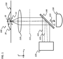
- FIG. 1 is a schematic that illustrates an exemplary embodiment of an optical imaging system.
- An optical imaging system 100 is configured to detect, image and investigate a specimen or a sample 20 including a nanoscale object 10.
- the optical imaging system 100 includes an imaging lens 110, an illumination source 120, a detector 130, and an optical element 140.
- the examples of the nanoscale object 10 may include macromolecules, proteins, extracellular vehicles, antigens, lipids, viruses, dye molecules, semiconductor quantum dot, metal nanoparticles, dielectric nanoparticles such as silica nanoparticles and polymer nanoparticles although the nanoscale object 10 is not limited to these examples.
- the sample 20 may comprise one or more of the following environments in which the nanoscale object 10 is embedded: aqueous environment, polymer matrix, organic crystal or semiconductor, a dielectric material.
- aqueous environment aqueous environment
- polymer matrix aqueous environment
- organic crystal or semiconductor a dielectric material.
- the composition of the sample 20 is not limited to these examples as long as the optical properties of the sample 20 allows optical imaging at the wavelengths of the illumination source 120.
- the illumination source 120 emits an excitation beam 121, 122.
- the optical element 140 is configured such that at least part of the excitation beam 121, 122 is at least partially reflected when incident on the optical element 140 and directed to the imaging lens 110.
- the optical element 140 is further configured to provide an optical path for the light reflected from the sample 20 towards the detector 130, separated from the optical path for the excitation beam 121, 122, as will be explained in more detail below.
- a sample interface 150 may be formed by a supporting material or a substrate which holds the sample 20 to be investigated and the sample.
- the sample interface 150 may be formed by a glass-air interface and the nanoscale object 10 may be supported on the glass surface.
- the nanoscale object 10 is on the upper side, a side of the sample interface 150 towards the positive z-direction, of the sample interface 150, the sample 20 including the nanoscale object 10 may be deposited on the lower side of the sample interface 150.
- the nanoscale object 10 may be deposited on a glass coverslip and the glass coverslip may be mounted such that the side of the glass coverslip with the nanoscale object 10 faces the imaging lens 110.
- the sample interface 150 is provided by the air-glass interface, in that the order of air and glass is reversed.
- the excitation beam 121, 122 may be reflected at the sample interface 150 and guided into the detector 130.
- the position of the nanoscale object 10 may be adjusted along the direction of the incoming excitation beam 121, 122, along the z-direction in FIG. 1 such that the nanoscale object 10 or the sample interface 150 is near the focal plane of the imaging lens 110 within the focal depth of the imaging lens 110 or equivalently within the focal volume of the imaging lens 110.
- the nanoscale object 10 or the sample interface 150 will be referred to be "in focus” or "at the focus” of the imaging lens 110.
- the position of the nanoscale object 10 may be adjusted moving the sample interface 150 along z-direction when the nanoscale object 10 is supported by the sample interface 150.
- the position of the glass surface in the z-direction may be adjusted by moving the glass on which the nanoscale object 10 is deposited.
- the examples of the imaging lens 110 includes an oil immersion objective lens, an air objective lens, aspheric lens, and an achromatic lens although the imaging lens 110 is not limited to these examples.
- the imaging lens 110 may be configured to provide a tight focusing of the excitation beam 121, 122, such as a diffraction-limited spot, and simultaneously to provide an efficient collection of the emission from the nanoscale object 10.
- the illumination source 120 may be arranged such that the excitation beam 121, upon entering the imaging lens 110, is focused at or near the sample interface 150 when the sample interface 150 is at the focus of the imaging lens 110.
- the excitation beam 121 represented with a solid line emanating from the illumination source 120 in FIG. 1 , is sent into the imaging lens 110 substantially collimated such that the excitation beam 121 is focused at the sample interface 150 or the nanoscale object 10 when the sample interface 150 or the nanoscale object 10 is at the focus of the imaging lens 110.
- the width of the excitation beam 121 in the xy-plane, is minimized near the sample interface 150 or the nanoscale object 10.
- This mode of illumination will be referred to as the confocal illumination in the rest of the specification.
- the spot size of the excitation beam 121 may be arranged to be diffraction-limited.
- the imaging lens 110 is an oil immersion objective lens and the sample interface 150 is formed by a glass coverslip and an aqueous sample and the space between the glass coverslip and the oil immersion objective lens 110 is filled with an immersion oil, a near diffraction-limited focal spot can be achieved.
- the illumination source 120 may be arranged such that the excitation beam 122, represented as dotted lines in FIG. 1 , is focused at or near a back-focal plane 111 of the imaging lens 110 and upon entering the imaging lens 110, illuminates an area around the nanoscale object 10 on the sample interface 150 such that a relatively large area, in xy-plane, is illuminated simultaneously.
- the transverse dimension of the area illuminated may be by a factor of ten or larger.
- the excitation beam 122 is at a visible wavelength
- the illuminated area at the sample interface 150 can be around ten microns across. In this case, the excitation beam 122 is not focused at the focal plane of the imaging lens 110. This mode of illumination will be referred to as the wide-field illumination in this specification.
- the illumination source 120 may include more than one excitation wavelength to facilitate more than one detection schemes.
- the optical element 140 may be configured to facilitate excitation of the sample 20 with more than one wavelength.
- the nanoscale object 10 may emit light depending on the mode of detection or the detection schemes.
- the nanoscale object 10 may emit light via fluorescence, Raman scattering and Rayleigh scattering, among others.
- fluorescence, Raman scattering and Rayleigh scattering among others.
- Each of these schemes may require a different configuration of the illumination source 120, the detector 130 and the optical element 140, as will be discussed in more detail later.
- the light emitted by the nanoscale object 10 may be polarised and the dipolar emission pattern of the nanoscale object 10 may be altered because the nanoscale object 10 is positioned close to the sample interface 150. In some implementations, the light emitted by the nanoscale object 10 may be isotropic, substantially uniformly distributed.
- At least part of the light emitted by the nanoscale object 10 may be collected by the imaging lens 110.
- the collection efficiency may depend on the sample interface 150, the numerical aperture of the imaging lens 110, the direction of the dipolar transition of the nanoscale object 10, among others.
- the optical element 140 may be configured to accommodate one or more of the detection schemes.
- the optical element 140 may be configured as a dichoroic or a polychroic, which is configured to reflect the light at the wavelength of the excitation beam 121, 122 incident on the optical element 140 and transmit the light at at least one of the wavelengths of the fluorescence light emitted from the nanoscale object 10.
- the fluorescence light collected by the imaging lens 110 may arrive at the detector 130 after being transmitted at the optical element 140.
- the optical element 140 is onfigured as a polarisation beam splitter at the wavelength of the excitation beam 121, 122 and of the scattered light from the nanoscale object 10. Both the reflected excitation beam 121, 122 and the scattered light may reach the detector 130 after being transmitted at the optical element 140.
- the detector 130 may be a single pixel detector such as an avalanche photodiode (APD), a photomultiplier tube (PMT) or a superconducting nanowire single-photon detector (SNSPD). All of the light collected by the imaging lens 110 and transmitted to the detector 130 may be detected with a single active area of the detector 130. This type of detector may be used with the confocal illumination where the excitation beam 121 is tightly focused on the nanoscale object 10 on the sample interface 150.
- APD avalanche photodiode
- PMT photomultiplier tube
- SNSPD superconducting nanowire single-photon detector
- the physical size of the nanoscale object 10 may be smaller than the diffraction limited spot of the excitation beam 121, 122 provided by the imaging lens 110.
- the nanoscale object 10 is imaged on the detector 130 as the diffraction limited spot in case the imaging lens 110 is configured as such.
- the detector 130 may be a multi-pixel detector or a multi-array detector such as a CCD, an EMCCD, a CCD, and a sCMOS. This type of detector may be used with the wide-field illumination where the excitation beam 122 is illuminated on the nanoscale object 10 on the sample interface 150 over a wide area and the collected light over the illuminated area is optically imaged onto the detector 130 over a plurality of pixels.
- the signal of interest comprises the light emitted from the nanoscale object 10, whose wavelength is displaced from the wavelength of the excitation beam 121, 122
- the light at the wavelength of the excitation beam 121 is rejected before reaching the detector 130.
- the signal of interest is the fluorescence light from the nanoscale object 10
- the excitation beam 121, 122 may be reflected from the sample interface 150 or scattered by the sample 20 and transmitted towards the detector 130.
- the rejection may be achieved mainly at the optical element 140 by configuring the optical element 140 to reflect or absorb the light at the wavelength of the excitation beam 121, 122.
- additional optics may be placed in the beam path, for example, between the optical element 140 and the detector 130, to further reject the light at the wavelength of the excitation beam 121. 122.
- additional optics may be introduced to further reject the light outside the wavelength range of the signal or interest.
- the background counts may include the spurious reflection of the excitation beam 121, 122 from various interfaces formed within the optical system 100, spurious emission from the sample 20, which are not rejected and filtered at the optical element 140 and reach the detector 130.
- the background counts may include the spurious reflection of the excitation beam 121, 122 from various interfaces formed within the optical system 100, spurious emission from the sample 20, which are not rejected and filtered at the optical element 140 and reach the detector 130.
- the imaging lens 110 is an objective lens
- intra-objective reflections arise from several surfaces inside the objective lens. Although these surfaces are AR coated, each surface has a reflectivity on the order of 0.1% at the wavelength of the excitation beam 121, 122. Therefore, the spurious reflection corresponds to the part the excitation beam 121, 122 which is generated by being reflected at the interfaces formed within the optical system other than the sample interface 150 and subsequently arrives at the detector 130.
- the background counts also include readout noise, dark counts or offset counts of the detector 130, which may be present even when no light impinges on the detector 130. Therefore, in this type of detection, the signal of interest is registered on top of the non-ideal, spurious background counts and the signal-to-noise ratio (SNR) may be improved by maximising the collection efficiency at the imaging lens 110 and by suppressing the background counts, namely rejecting all of light reaching the detector 130 other than the light comprising the signal of interest and minimising the spurious counts at the detector 130.
- this type of detection schemes will be referred to as the emission-based detection scheme.
- the fluorescence detection scheme is an example of the emission-based detection scheme.
- the optical imaging system 100 is also configured for the interferometric scattering microscopy (iSCAT) scheme.
- iSCAT interferometric scattering microscopy
- the nanoscale object 10 is detected by the interference pattern between the scattered light from the nanoscale object 10 and the reflected excitation beam 121, 122 reflected at the sample interface 150.
- the signal from the iSCAT scheme results from the interference between two light fields: the electric field of the scattered light 11 and the electric field of the reference light 123.
- the scattered light 11 is the light that is scattered by the nanoscale object 10 inside the focal volume at the focus of the imaging lens 110. Part of the scattered light 11 is collected by the imaging lens 110 and imaged onto the detector 130.
- the reflected excitation beam 121, 122 reflected at the sample interface will be referred to as the reference light 123 for the rest of the specification.
- the scattered light 11, the signal of interest, and the reflected excitation beam 121, 122, reference light 123 are at the same wavelength. Therefore, the optical element 140 is configured to function as a beam splitter.
- the scattered light 11 and the reference light 123 are made to follow a different path and therefore separated from the excitation beam 121, 122 by a beam splitter.
- the optical signal detected on the detector 130 is an interferometric signal caused by the interference between the scattered light 11 from the nanoscale object 10 and the reference light 123.
- E inc is the incident electric field, which corresponds to the electric field of the excitation beam 121, 122 at the sample interface 150.
- s is a unitless parameter related to the particle scattering cross-section and the optical properties of the sample interface 150.
- r 2 is the reflectivity of the sample interface 150.
- ⁇ is the phase difference between the reference light and the scattered light at the detector 130.
- the optical path length difference of the scattered light 11 and the reference light 123 are minimised to be smaller than the focal depth of the imaging lens 110 at the excitation wavelength.
- the scattered light 11 from the nanoscale object 10 when it is out of focus, it may still interfere with the reference light because the coherence length of the excitation beam 121, 122 may be longer than the resulting optical path length difference. Also, the excitation beam 121, 122 may be reflected off other interfaces formed within the optical imaging system 100 other than the sample interface 150 and interfere with the scattered light from the nanoscale object. These, spurious interference signals or false signals, may lead to the degradation of the signal-to-noise ratio or axial resolution.
- the illumination source 120 may be chosen or configured such that the coherence length of the excitation beam 121, 122 is shorter than the path length difference between the spurious reflection and the excitation beam 121, 122.
- the illumination source 120 may be configured such that its coherence length is shorter than 100 microns if the path length difference between the spurious reflection and the excitation beam 121, 122 is larger than a millimetre. This may mitigate the interference between the scattered light and the spurious reflection and the spurious interference detected at the detector 130 only contributes as an incoherent background, not as a false signal.
- the optical contrast C can be made arbitrarily large, in practice, this is not the case due to the imperfections in the optical imaging system 100, such as the spurious reflection of the excitation beam 121, 122 reaching the detector 130. These still contribute to the background level on the detector 130 and the corresponding fluctuations contribute to the noise level. Therefore, in case the optical contrast C is to be improved, the reflectivity at the sample interface 150 needs to be adjusted considering the non-idealities or imperfections.
- the optical imaging system 100 can be configured to accommodate other detection methods than the iSCAT detection scheme by correspondingly configuring the illumination source 120 and the optical element 140, for example one of the emission-based detections. In this case, there can be stray light from the spurious reflection of the excitation beam 121 for the other detection scheme or due to the imperfections of the optical element 140.
- the optical element 140 may be arranged to function as a beam splitter for the iSCAT mode and simultaneously to function as a dichroic mirror for the fluorescence mode.
- the fluorescence light emitted from the nanoscale object 10 is transmitted at the optical element 140 and the reflected excitation beam 121, 122 are either reflected or absorbed at the optical element 140.
- the degree of rejection of the reflected excitation beam 121, 122 may be imperfect, in which case the optical element may allow some of the reflected excitation light 121, 122 to reach the detector 130. This contributes to the background noise of the fluorescence detection scheme.
- the current iSCAT detection schemes may be improved on the following fronts:
- the optical contrast may be further enhanced.
- the particle scattering cross-section of biological molecules depends on the molecular mass; therefore a measurement of the iSCAT contrast can be used to determine the molecular mass of the particle of interest. Since the strength of the scattering is a characteristic of the mass of the nanoscale object 10, the iSCAT method enables label-free imaging of individual macromolecules and nanoparticles.
- the optical contrast may be small for small biological molecules. Since in the iSCAT detection scheme, different molecules can only be distinguished by their optical contrast, i.e. by their mass, a higher optical contrast may lead to a higher specificity in the detection of biological molecules.
- the saturation level of the detector 130 may limit the optical power of the excitation beam 121, 122, which may limit the achievable signal-to-noise ratio.
- the signal of interest is registered as a deviation, either as an increase or decrease, from the power level of the reference light 123. Therefore, to increase the signal-to-noise ratio (SNR), the power level of the reference light 123 impinging on the detector 130 may be high enough such that the contributions from the detected signal from stray light, spurious reflections, detector readout noise are dominated by the reference light 123 impinging on the detector 130.
- the power level of the reference light 123 should be sufficiently below saturation level of the detector 130.
- a detector 130 suitable for the emission-based detection may not be suitable for the iSCAT detection scheme.
- the optical imaging system 100 is configured to accommodate more than one detection schemes including the iSCAT detection scheme and one or more of the emission-based detection schemes, such as fluorescence detection, dedicated detectors 130 for the iSCAT detection and for the emission-based detection may be needed. This is because in order to achieve a high signal-to-noise ratio with a signal with a low power level, the emission-based detection often employs a detector 130 with a low saturation level, which may not be compatible with the power level of the reference light 123 of the iSCAT detection scheme.
- the current specification provides an optical imaging system 100 which addresses the issues discussed above.
- the reflectivity at the sample interface 150 is configured such that the reference light 123 is decreased to a level where the iSCAT scheme is compatible with the detector 130 used for emission-based detection schemes. Therefore, one detector 130 may be used both for the iSCAT detection scheme and an emission-based detection scheme, such as fluorescence detection.
- the level of the power of the reference light 123 impinging on the detector 130 also decreases. This leads to an improved optical contrast compared to the case where the sample interface 150 is untreated, for example, a glass-water interface.
- the signal-to-noise ratio of the iSCAT detection scheme may be improved because a larger power of the excitation beam 121, 122 can be used without saturating the detector 130. Therefore, the reflectivity of the sample interface 150 may be determined to optimise the signal-to-noise ratio, considering the available power of the excitation beam 121, 122 and the corresponding power level of the reference light 123 impinging on the detector 130. This will be discussed in more detail later.
- the optical imaging system 100 which facilitates a concurrent operation of the iSCAT detection scheme and the fluorescence detection scheme will be described below.
- a procedure to determine the reflectivity of the sample interface 150 will be discussed.
- the design of the optical coating on the sample interface 150 and the optical element 140 will follow.
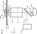
- FIG. 2a is a schematic that illustrates an exemplary embodiment of an optical imaging system.
- the optical imaging system 200 includes an imaging lens 210, an illumination source 220, a detector 230, an optical element 240.
- the optical imaging system 200 may be configured for the iSCAT detection scheme and the fluorescence detection scheme, as discussed below.
- the detector 230 may be a multi-pixel detector or a multi-array detector such as a CCD, an EMCCD, a CCD and a sCMOS. In some implementations, one and the same detector 230 may be used for both the iSCAT detection scheme and the fluorescence detection scheme.
- the imaging lens 210 may be a high-magnification, high-numerical aperture lens or lens system such as an oil immersion objective lens, an air objective lens, aspheric lens, and an achromatic lens.
- the imaging lens 210 may be a high-NA oil immersion objective lens.
- a sample 40 may include one or more of nanoscale objects 30.
- the sample 40 may be an aqueous solution deposited and supported on a substrate 251, for example a glass coverslip.
- the substrate 251 may comprise a material which is substantially transparent at the wavelength of excitation and at the wavelength of the signal of interest, emitted from the nanoscale object 30.
- FIG. 2a only shows one nanoscale object 30 within the sample 40, an aqueous solution, for illustration purposes. However, it is understood that the sample 40 can contain an arbitrary number of the nanoscale objects 30 as necessary.
- the substrate 251 includes an optical coating 25 2 on a side facing the sample 40 such that the optical coating 25 2 is disposed between the substrate 251 and the sample 40.
- the optical coating 252 may be in direct contact with the aqueous solution.
- the optical coating 252 may be directly deposited on a side of the substrate 251.
- a sample interface 250 may be formed between the optical coating 252 and the sample 40.
- the sample interface 250 may lead to the reflection of incident light due to the arrangement of the refractive indices of the sample interface 250.
- the sample interface 250 may correspond to a glass-water interface.
- the reflection is due to the Fresnel reflection at the glass-water interface.
- the optical coating 252 may be a Bragg reflector including a plurality of dielectric layers, designed in view of the refractive indices of the substrate 251 and the sample 40.
- the sample interface 250 which determines the degree of reflection of the excitation beam 221, may vary depending on the material choices of the substrate 251 and the sample 40, in addition to the design of the optical coating 252, as will be described later.
- the space between the substrate 251 and the imaging lens 210 may be arranged such that the number of interfaces leading to Fresnel reflection is minimised and Fresnel reflection at remaining interfaces is mitigated.
- the gap between the substrate 251 and the imaging lens 210 may be filled with an immersion oil 211 for index-matching.
- the nanoscale objects 30 may move around within the aqueous solution of the sample 40 and may be detected when they move close to the sample interface 250 and the illuminated area, or equivalently within the illumination volume or the focal volume.
- the illumination source 220 may include a plurality of light sources or a plurality of excitation wavelengths to facilitate more than one detection schemes or to facilitate more than one type of nanoscale objects 30, emitting light at different wavelengths.
- the illumination source 220 includes an excitation source for the iSCAT detection scheme and the fluorescence detection scheme.
- the illumination source 220 may include more than one excitation wavelengths to facilitate the use of a plurality of fluorophores with different fluorescence spectra for multi-colour fluorescence detection.
- the illumination provides the excitation light 221 such that the sample 30 is excited by wide-field illumination by focusing the excitation light 221 at the back focal plane 212 of the imaging lens, an oil immersion objective lens.
- the illumination source 220 includes a plurality of light sources, the multiple beams may be arranged to follow substantially the same path of the excitation light 221 described in FIG. 2a , represented by dotted lines for the wide-field illumination at the sample 40.
- an excitation beam 221 emanating from the illumination source 220 is reflected.
- a reference light 222 is the part of the excitation beam 221 that is reflected by the sample interface 250.
- the degree of reflection may be dependent on the optical coating 252, the refractive index of the substrate 251, and the refractive index of the sample 40.
- the reference light 222 is guided towards the detector 230.
- the scattered light 31 may comprise light due to scattering processes.
- the scattered light 31 may be at the same wavelength as the excitation beam 221.
- the scattered light 31 may be at a different wavelength than the excitation beam 221, in this specification the scattered light 31 is taken to be at the same wavelength as the excitation beam 221, unless otherwise noted.
- the emission light 32 may comprise light originating from photophysical process of the nanoscale object 30 in response to absorbing part of the excitation beam 221.
- the emission light 32 may not maintain a coherent phase relationship with the excitation beam 221 therefore may not lead to any interference pattern with the reference light 222.
- the emission light 32 may comprise emission via fluorescence, phosphorescence or emission arising from electron-hole recombination.
- the emission light 32 will be used in this specification as, or interchangeably with the fluorescence light 32.
- the fluorescence light 32 is used to refer to the part of the emission from the nanoscale object 30 which does not lead to interference pattern with the excitation beam 221. Therefore, the fluorescence light 32, for example, includes red-shifted emission from the colloidal quantum dots or phosphorescence from a phosphor molecule.
- the reference light 222, the scattered light 31 and the emission light 32 follow substantially the same optical path starting from the sample interface 250 to the detector 230.
- the difference in optical path lengths between the reference light 222 and the scattered light 31 or between the reference light 222 and the emission light 32 may be less than the length of the coherence length of the reference light 222.
- the optical contrast and the signal-to-noise ratio of the iSCAT detection scheme will be presented in terms of various parameters describing the optical imaging system 200. Based on these descriptions, the target reflectivity of the sample interface 250 to optimise the signal-to-noise ratio of the iSCAT detection scheme will be derived.
- N det T exp N inc ⁇ P area / M 2 r + e i ⁇ sqrt ⁇ s 2 + T exp N inc ⁇ P area / M 2 ⁇ + T exp ⁇ + ⁇
- the optical contrast or the signal-to-background ratio can be calculated by comparing the number of detected photons with and without the nanoscale object 30.
- the noise originates from the intensity fluctuations on each pixel, caused for example by the camera readout noise and the photon shot noise.
- the standard deviation of these fluctuations is estimated by the square root of N det given in equation 3.
- Sqrt( x ) represents a square root of x in this specification.
- the design of the optical coating 252 the details of the optical arrangement of the optical imaging system 200 as well as noise properties of the detector need to be taken into account.
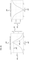
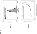
- FIG. 2b is a graph that shows the estimation of the optical contrast and the signal-to-noise ratio of the iSCAT detection scheme as a function of the reflectivity at the sample interface.
- the optical contrast is evaluated using equation 4 and the signal-to-noise ratio is evaluated using equation 6.
- the rest of the parameters are set as given as typical values in equation 3, except the optical power used, corresponding to N inc , is 3 kW/cm 2 .
- the saturation level of the detector 230, a CMOS camera, 30 ⁇ 10 3 photo-electrons per frame or per exposure time and the maximum available input power of the illumination source 220, 10 mW at 450 nm were further considered as constraints in the evaluation.
- Illumination area at the sample interface 250 had a diameter of approximately 10 ⁇ m.
- a left panel 280 shows a plot of the signal-to-noise ratio, represented in the vertical axis 282 on the left, as a function of the reflectivity at the sample interface 250, represented in the horizontal axis 281.
- the illumination intensity is adjusted so that the detector 230 operates close to saturation. For example, at a higher reflectivity, for example towards 10 -2 , the illumination power is most attenuated from the available power of 10 mW at the illumination source 220, before entering the imaging lens 210 not to saturate the detector 230.
- the incident laser power is plotted in the left panel 280 in a dotted line and represented in the vertical axis 283 on the right.
- a first range 284 from around 10 -5 reflectivity at the sample interface 250 and higher, the laser power is attenuated to avoid saturation of the detector 230.
- the intensity of the light 221 impinging on the detector 230 is close to saturation of the detector 230. Therefore, it may be that the photon shot noise dominates other sources of noises such that the signal-to-noise ratio of the iSCAT detection is near shot-noise-limited.
- the plot in the left panel 280 also shows that the signal-to-noise ratio is the highest at a reflectivity of around 2 ⁇ 10 -5 and again decreases as the reflectivity further decreases. This is due to the fact that in a second range 285, from the reflectivity of around 2 ⁇ 10 -5 and lower, even if the full power of 10 mW of the excitation beam 221 is sent into the imaging lens 210, the detector 230 is not operated close to saturation by the reference light 222. Therefore, for the reflectivity in the second range 285, the signal-to-noise ratio of the iSCAT detection may not be limited by the photon shot-noise of the reference light 222 and other noise sources contribute to the noise ⁇ det as discussed above in equation 6. Since the intensity of the excitation beam 221 at the sample interface 250 is fixed from using the full power of 10 mW over this range of reflectivity, from around 2 ⁇ 10 -5 to a smaller reflectivity, the signal-to-noise ratio decreases.
- a right panel 290 shows a plot of the optical contrast, or the signal-to-background ratio, represented in the vertical axis 292, as a function of the reflectivity at the sample interface 250, represented in the horizontal axis 291.
- the optical contrast is plotted as a negative quantity. For example, the optical contrast of 0, the highest point in the vertical axis 292, represents the background level without any interference signal.
- the illumination intensity is adjusted so that the detector 230 operates close to saturation.
- full power of 10 mW of the excitation beam 221 can be sent into the imaging lens 210 without saturating the detector 230.
- the plot in the right panel 290 shows that the optical contrast is the highest at a reflectivity of 10 -5 .
- the terms which are not proportional to N inc such as T exp * ⁇ + ⁇ in equation 3, are negligible.
- the optical contrast is maximised when the reflectivity at the sample interface 250 equals ⁇ , which is a dimensionless number representing the spurious reflection of the excitation beam 221 from the interfaces along the beam path other than the sample interface 250 and set to be 10 -5 in this evaluation.
- one of the limiting factors to the optical contrast may be the degree of spurious reflections caused by the excitation beam 221, represented by ⁇ in equation 3.
- the optimal reflectivity or target reflectivity at the sample interface 250 is determined taking into account the following considerations.
- the optical contrast increases when the reflectivity at the sample interface 250 is reduced. Also it can be shown that the signal-to-noise ratio is proportional to the square root of N inc under the same condition. However, these correspond to an idealised case where other spurious sources contributing to the background, for example the degree of spurious reflection ⁇ are not considered.
- the background N bg is dominated by the reflection at the sample interface 250 N inc r 2 and the spurious reflection N inc ⁇ .
- the reflectivity at the sample interface 250 may be determined in view of the available optical power of the illumination source 220 such that the power of the reference light 222, or the reflected excitation beam 221 impinging on the detector 230 is below the saturation level of the detector 230 but high enough. This is such that the photon shot-noise of the reference light 222 dominates or is substantially larger than the other sources of noise, which includes readout offset count of the detector 230, represented as ⁇ , stray light from other light sources, represented as ⁇ . Also, the reflectivity at the sample interface 250 may be determined such that the intensity of the illumination light at the sample is low enough to avoid damaging the sample, which causes phototoxicity in biological samples.
- the signal-to-noise ratio was maximised at a different value of the reflectivity, 2 ⁇ 10 -5 , than the optical contrast in the right panel 290.
- the reflectivity of the sample interface 250, and the correspondingly the optical power of the excitation beam 221 can be chosen to maximise the signal-to-noise ratio, i.e approximately 2 ⁇ 10 -5 in this example, even at the expense of optical contrast.
- the reflectivity at the sample interface 250 may be chosen to be higher than the degree of spurious reflection ⁇ and lower than the reflectivity at the sample interface 250 without the optical coating 252.
- the optical coating 252, to be deposited on the substrate 251 to provide the target reflectivity can be designed.
- FIG. 3a is a schematic that illustrates an exemplary embodiment of an optical coating to form a sample interface with references to FIG. 2a .
- an optical coating 252, 300 is designed taking into account of additional experimental parameters such as the wavelength of the excitation beam 221, the refractive index of the substrate 251, the refractive index of the sample 30, the angle-of-incidence of the excitation beam 221 and biocompatibility of the material.
- the wavelength can be between 400 to 800 nm.
- the wavelength can be 450nm.
- the material of the substrate 251 may comprise borosilicate glass.
- the substrate 251 may be a borosilicate glass microscope coverslip.
- the imaging lens 210 for example, an oil immersion objective lens, may be optically corrected for the thickness and the refractive index of the substrate 251.
- the substrate 251 may be a part of a microfluidic channel comprising a material optically transparent at the wavelength of excitation beam 221.
- the substrate 251 may be an elastomeric material or thermoplastic material, which is transparent at the excitation wavelength.
- the substrate 251 may be a part of glass microscope slide, optical fiber or a prism or a microtiter plate.
- the substrate 251 may comprise optically transparent polymer.
- a sample interface 250, 350 is formed between a surface of the substrate 251 to face the sample 40 and an optical coating 252, 300 deposited on the substrate 251.
- the sample interface 250, 350 may determine the degree of reflection of the excitation beam 221 towards the detector 230, therefore the intensity or power of the reference light 222.
- the optical coating 252, 300 may comprise one or more layers, each layer with a predetermined refractive index. Each layer of the optical coating 252, 300 may be disposed substantially parallel to the face of the substrate 251 facing the sample 30.
- the optical coating 252, 300 may comprise a single layer with a uniform refractive index.
- the layer of the optical coating 252, 300 in contact with the substrate 251 may have a refractive index different from the refractive index of the substrate 251.
- the excitation beam 121, 122, 221 may be mainly reflected via Fresnel reflection by the refractive index contrast between the substrate 251 and the sample 40.
- the sample interface may be formed by the substrate 251 and the sample 40.
- the sample interface 250, 350 may be provided by a plane defined by the index contrast between two materials with two different refractive indices.
- the sample interface may be provided by an optical arrangement near the nanoscale object 30 to be imaged, which contributes to the degree of reflection of the excitation beam 221 near the position of the nanoscale object 30 of the sample 40 when the nanoscale object 30 is in focus.
- the optical arrangement which determines the degree of reflection is provided by the optical coating 252 such as the optical coating 300 presented in FIG. 3a .
- a first side 252-1 of the optical coating 252, 300 may be directly in contact with the surface of the substrate 251.
- a second side 252-2 of the optical coating 252, which is not in contact with the surface of the substrate 251 may be exposed towards the sample 40 such that when the sample 40 is applied, the second side 252-2 of the optical coating 252 is in direct contact with the sample 40.
- the optical coating 252, 300 may be fabricated on the substrate 251.
- the layers included in the optical coating 252, 300 may be deposited on the substrate 251 via one or more fabrication techniques including ion-beam sputtering, sputter deposition such as physical vapour deposition, atomic layer deposition or spin coating. Any known techniques to form a dielectric layer or an organic/inorganic layer may be used to fabricate the optical coating 252, 300 on the substrate 251.
- the optical coating 252, 300 may be fabricated separate from the substrate 251, for example, on a separate substrate, and subsequently transferred on the surface of the substrate 251.
- the optical coating 252, 300 may be attached to the substrate via van der Waals bonding or using a thin layer of adhesive.
- the optical coating 252, 300 may have a refractive index or an effective refractive index different to those of the sample 40 and the substrate 251.
- the optical coating 252, 300 may alter the reflectivity of the excitation beam 221 incident on the substrate 251, for example, travelling in positive z-direction, at the sample interface 250, 350 from the reflectivity given from the sample interface 250, 350 formed by the substrate 251 and the sample 40.
- the angle-of-incidence of the excitation beam 221 may deviate from 0 degree with respect to the central axis of the imaging lens 210, along the z-direction, and may be less than 10 degrees.
- the angle-of-incidence of the excitation beam 221 may be chosen to alleviate the spurious reflections, quantified above as ⁇ by reducing the overlap between the spurious reflection and the reference light 222.
- the optical coating 252, 300 may be designed taking the angle-of incidence of the excitation beam 221 into consideration.
- the optical coating 252, 300 may comprise two or more layers 310, 320.
- the number of layers and the refractive indices of the layer 310, 320 may be chosen such that the reflectivity is adjusted close to the target reflectivity due to the interference effects of the layers 310, 320.
- the optical coating 252, 300 may be designed taking the refractive index of the substrate 251 and the sample 40 into consideration.
- the optical coating 252, 300 may be designed considering the physical dimensions of the substrate 251 such as the thickness.
- the optical coating 252, 300 may be designed to achieve a reflectivity at the sample interface 250, 350 of 0.1% to 0.001%, for example 0.01%.
- the optical coating 252, 300 may be designed to achieve a reflectivity at the sample interface 250, 350 equal to the degree of the spurious reflection, quantified above as ⁇ .
- the optical coating 252, 300 may comprise a first layer 310 and a second layer 320.
- the coating 252, 300 may be kept simple, inexpensive and thin while the reduction of the reflectivity can be achieved for a particular wavelength and a particular range of angle of incidence.
- the first layer 310 may comprise a dielectric material or metal oxides, such as one or more of Al 2 O 3 , HfO 2 , Ta 2 O 5 , Nb 2 O 5 , SiO 2 and TiO 2 .
- the intermediate layer comprises a transparent conducting oxide such as indium tin oxide (ITO).
- ITO indium tin oxide
- the thickness t1 of the first layer 310 may be between 1 nm and 20 nm.
- the first layer 310 may be 6nm.
- the second layer 320 may comprise a material which is non-toxic and highly biocompatible. Since the second layer 320 can be in contact with the sample 40 the material of the second layer 320 may be chosen to be compatible with biological samples and biomedical assays and amenable to surface functionalisation chemistry on the sample interface 250, 350.
- the second layer 320 may comprise SiO 2 .
- the surface comprising Al 2 O 3 , HfO 2 , Ta 2 O 5 , Nb 2 O 5 and TiO 2 may also be functionalised and treated to be biocompatible.
- the thickness t2 of the second layer 320 may be between 80 nm and 200 nm.
- the first layer 310 may comprise Ta 2 O 5 with a thickness of 4 nm and the second layer 320 comprises SiO 2 with a thickness of 106 nm.
- the thickness of the first layer 310 may be between 1 and 10 nm, and the thickness of the second layer 320 may be between 80 and 200 nm.
- the substrate 251 may be a high-precision cover glasses made from borosilicate glass D 263 with thickness No. 1.5H, representing the tolerance in thickness of 170 ⁇ m ⁇ 5 ⁇ m.
- the borosilicate glass, Ta 2 O 5 is deposited as the first layer 310 with a thickness of 4 nm and SiO 2 is deposited as the second layer 320 with a thickness of 106 nm, via ion-beam sputtering.
- the ion-beam sputtering was adopted because it allows a precise thickness control.
- the coating i.e. the number of layers, layer thicknesses and layer materials
- the coating is designed using established tools for the design of the optical coating 252, 300.
- the design, for example numerical optimisation, and the fabrication of the optical coating 252, 300 may be analogous to those for the design and the fabrication of an antireflection coating. Therefore, as long as a desired reflectivity can be achieved at the sample interface 250, 350, the implementation of the optical coating 252, 300 is not limited to a two-layer structure on a glass coverslip, as shown in the example of FIG. 3a .
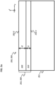
- FIG. 3b shows simulation results of the reflectivity of the optical coating.
- the optical coating 252, 300 is assumed to consist of tantalum pentoxide (Ta 2 O 5 ) as the first layer 310 with a thickness of 4 nm and silicon dioxide (SiO 2 ) as the second layer 320 with a thickness of 106 nm. It is assumed that water is in contact with the SiO 2 layer and the glass coverslip comprises borosilicate glass D.
- Ta 2 O 5 tantalum pentoxide
- SiO 2 silicon dioxide
- An upper panel 360 shows a graph which shows the reflectivity at 0 degree angle-of-incidence (AOI) as a function of the wavelength on an untreated glass coverslip, labelled as 'uncoated glass' and on a glass coverslip containing the optical coating 252, 300, labelled as 'coated glass'.
- AOI angle-of-incidence
- the reflectivity is 0.01 %.
- the reflectivity at 0 AOI can be determined to enhance the optical contrast and the signal-to-noise ratio as explained above.
- the optical coating 252, 300 is deposited on the substrate 251 to reduce the reflectivity from 0.43 to 0.01 %. From around 600 nm wavelength and higher the reflectivity of the coated glass coverslip approaches the reflectivity of the uncoated glass coverslip.
- a lower panel 370 shows a graph which shows the reflectivity at 40 degrees angle-of-incidence (AOI) as a function of the wavelength on an untreated glass coverslip, labelled as 'uncoated glass' and on a glass coverslip containing the optical coating 252, 300, labelled as 'coated glass'.
- AOI angle-of-incidence
- the reflectivity is around 0.8 %. From around 550 nm and higher, the reflectivity of the coated coverslip and the uncoated coverslip are close to each other.
- the thickness of the first layer 310 may be between 1 and 10 nm and the thickness of the second layer 320 may be between 80 and 200 nm.
- FIGS. 4a and 4b show measurement results obtained using the iSCAT detection scheme.
- the experimental results shown in FIGS. 4a and 4b were obtained using the optical imaging system 200 described in FIG. 2a with the following specifications:
- the imaging lens 210 is a high numerical aperture oil immersion objective lens.
- the substrate 251 is a high-precision cover glasses made from borosilicate glass D 263 with thickness No. 1.5H, representing the tolerance in thickness of 170 ⁇ m ⁇ 5 ⁇ m.
- cover glass and “coverslip” will be used interchangeably.
- the optical coating 252, 300 on the substrate 251 Ta 2 O 5 was deposited as the first layer 310 with a thickness of 4 nm and SiO 2 is deposited as the second layer 320 with a thickness of 106 nm.
- an aqueous sample 40 including the nanoscale objects 30 was applied on top of the cover glass 251, both coated or uncoated, to observe the difference in the optical contrast and in the signal-to-noise ratio.
- coated coverslip will be used to mean the cover glass 251 and the optical coating 252, 300 described above.
- uncoated coverslip or “untreated glass” will be used to mean the cover glass 251 described above, unless otherwise noted.
- the sample interface 250 at which the excitation beam 221 is reflected to provide the reference light 222 for the iSCAT detection scheme, is formed by the arrangements of the substrate 251, the optical coating 250, and the sample 40.
- the sample interface 250 is formed by the refractive index contrast of the substrate 251 and the sample 40, in other words, a glass-water interface.
- the experimental protocol was as follows:
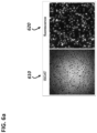
- FIG. 4a shows comparison of the measurement results of the optical contrast obtained with and without the optical coating 252, 300 deposited on the substrate 251.
- the nanoscale objects 30 are gold nanoparticles with a nominal mean diameter of 10 nm.
- Both images, recorded respectively using a coated glass coverslip and an uncoated glass coverslip comprise 200 x 200 pixels, corresponding to 6 ⁇ m x 6 ⁇ m on the sample interface 250, 350.
- the upper image, taken with the coated glass coverslip is an average of 100 frames, each taken with 250 frames per second integration time.
- the lower image, taken with the uncoated coverslip is an average of 100 frames, each taken with 1000 frames per second integration time.
- the measurement result shows that for the uncoated coverslip, the optical contrast is 1-2 % while for the coated coverslip, the optical contrast is 8-10 %.
- An upper right panel 420 of FIG. 4a shows two histograms, a left histogram 421 and a right histogram 422, which show the measurements of the optical contrasts obtained using gold nanoparticles as the nanoscale objects 30.
- the left histogram 421 shows statistics of the measurements made with gold particles with a mean diameter of 5 nm.
- the mean optical contrast is around 0.45 %.
- the number of particles for the measurements with the untreated glass coverslip was 227.
- the mean optical contrast is around 3.1 %.
- the number of particles for the measurments with the coated glass coverslip was 185.
- the measurement data suggests that the enhancement of the optical contrast is around sevenfold when the coated glass coverslip is used.
- the right histogram 422 shows statistics of the measurements made with gold particles with a mean diameter of 20 nm.
- the mean optical contrast is around 7.8 %.
- the number of particles for the measurements with the untreated glass coverslip was 114.
- the mean optical contrast is around 62 %.
- the number of particles for the measurments with the coated glass coverslip was 186.
- the measurement data suggests that the enhancement of the optical contrast is around eightfold when the coated glass coverslip is used.
- the imaging lens 210 used was a high numerical aperture oil immersion objective lens with NA 1.40 and a magnification of 111.
- the nanoscale objects 30 are Fibrinogen with a mass of 340 kDa.
- Both images, recorded respectively using a coated glass coverslip and an uncoated glass coverslip comprise 160 x 160 pixels, corresponding to 4.7 ⁇ m x 4.7 ⁇ m on the sample interface 250, 350.
- the upper image, taken with the coated glass coverslip is an average of 100 frames, each taken with 250 frames per second integration time.
- the lower image, taken with the uncoated coverslip is an average of 1000 frames, each taken with 1000 frames per second integration time.
- the measurement result shows that for the uncoated coverslip, the optical contrast is around 0.08 % and that for the coated coverslip, the optical contrast is around 0.6 %.
- the nanoscale objects 30 are Thyroglobulin with a mass of 660 kDa.
- Both images, recorded respectively using a coated glass coverslip and an uncoated glass coverslip comprise 200 x 200 pixels, corresponding to 6 ⁇ m x 6 ⁇ m on the sample interface 250, 350.
- the upper image, taken with the coated glass coverslip is an average of 100 frames, each taken with 250 frames per second integration time.
- the lower image, taken with the uncoated coverslip is an average of 100 frames, each taken with 1000 frames per second integration time.
- the measurement result shows that for the uncoated coverslip, the optical contrast is around 0.2 % and that for the coated coverslip, the optical contrast is around 1.5 %.
- FIG. 4b shows comparison of the measurement results of the optical contrast obtained and the signal-to-noise ratio with and without the optical coating 252, 300 deposited on the substrate 251.
- the nanoscale objects 30 are GroEL protein with a mass of 840 kDa.
- Both images, recorded using a coated glass coverslip and an uncoated glass coverslip comprise 240 x 240 pixels, corresponding to 14 ⁇ m x 14 ⁇ m on the sample interface 250, 350.
- the upper image, taken with the coated glass coverslip is an average of 150 frames, each taken with 500 frames per second integration time.
- the lower image, taken with the uncoated coverslip is an average of 150 frames, each taken with 500 frames per second integration time.
- the measurement result shows that for the uncoated coverslip, the optical contrast is 0.24 % after 150 frames average and that for the coated coverslip, the optical contrast is around 1.67 % after 150 frames average.
- a histogram shows a statistics of the optical contrast obtained with the nanoscale objects 30 are GroEL protein with a mass of 840 kDa with and without the optical coating 252, 300 on the substrate 251.
- the measurement results of FIG. 4b shows that the optical coating 252, 300 as part of the sample interface 150, 250, disposed on the substrate 251 enhances the signal-to-noise ratio compared to the case where the sample interface 150, 250 is formed by the interface between the substrate 251 and the sample 20, 40.
- the reduced reflectivity at the sample interface 150, 250 by depositing the optical coating 252, 300 on the substrate may enable simultaneous operation of the iSCAT detection scheme and the fluorescence detection scheme on the same setup using one multi-arrayed detector, as will be discussed below.
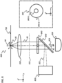
- FIG. 5 is a schematic that illustrates an exemplary embodiment of an optical imaging system.
- the optical imaging system 500 is configured to facilitate both the iSCAT detection scheme and the fluorescence detection scheme for optical investigation of a sample 60 that includes one or more nanoscale objects 50.
- the optical imaging system includes an imaging lens 510, an illumination source 520, a detector 530, and a first optical element 540.
- the nanoscale objects 50 may include several groups of different fluorophores or nanoparticles which can be used for different detection schemes and for different excitation/detection wavelengths.
- the examples of the nanoscale objects 50 may include macromolecules or gold nanoparticles.
- the nanoscale objects 50 may include several types of fluorophores, each with different excitation and fluorescence spectra, for example, for multi-colour fluorescence imaging.
- one species of the nanoscale objects 50 may be detected via both the iSCAT detection scheme and the fluorescence detection scheme.
- a fluorescence bead, a fluorescently labelled protein or a CdSe/ZnS semiconductor quantum dot may be imaged both via the fluorescence detection scheme and the iSCAT detection scheme.
- the examples of the imaging lens 510 may include a high numerical aperture (NA) oil immersion objective lens and a high numerical aperture (NA) air objective.
- NA numerical aperture
- the imaging lens 510 is taken to be a high numerical aperture oil immersion objective lens, unless otherwise noted.
- other types of imaging optics can be employed for the imaging lens 510 for the optical imaging system 500.
- the illumination source 520 may include a plurality of illumination sources arranged to provide multiple wavelengths of excitation light, to facilitate more than one detection scheme or to facilitate the use of multiple fluorophores with different colours.
- the illumination source 520 includes a first illumination source 521 and a second illumination source 522.
- the first illumination source 521 provides a first excitation beam 521a for the iSCAT detection scheme.
- the first illumination source 521 may be a laser at 450 nm wavelength used to detect the nanoscale object 50, for example, gold nanoparticles, via the iSCAT detection scheme.
- the first excitation beam 521a may be linearly polarised.
- the first excitation beam 521a may be launched from a polarisation maintaining fibre 523.
- the first illumination source 521 may output the first excitation beam 521a polarised from the inherent configuration of the first illumination source 521.
- the first illumination source 521 may comprise a low-coherence light source.
- the first illumination source 521 may comprise a compact, high-power superluminescent light emitting diode coupled to a polarisation-maintaining fibre.
- the first illumination source 521 may comprise a single-mode diode laser with a fast current modulation, for example, at a modulation frequency 300 MHz.
- the nanoscale object 10, 30, 50 is imaged by the optical contrast of the interference pattern between the reference light 123, 222 and the scattered light 11, 31.
- the coherence length the first excitation beam 521a may be rendered as short as possible or the first illumination source 521 with a short coherence length may be chosen such that the interference between the scattered light 11, 31 and the spurious reflection may be mitigated in that the spurious reflection contributes to incoherent noise background, rather than a spurious interference pattern.
- the second illumination source 522 provides a second excitation beam 522a for the fluorescence detection scheme.
- the second illumination source 522 may be a laser with a wavelength that overlaps with an excitation spectrum or an absorption spectrum of the nanoscale object 50 within the sample 60.
- the nanoscale object 50 in this case may be a fluorescent tag or a fluorophore such as an organic dye molecule, a fluorescent protein, a colloidal quantum dot, or a fluorescence bead.
- the second illumination source 522 may comprise a plurality of light sources, each capable of emitting an excitation light within a preselected wavelength band correlated with the respective excitation spectrum of a plurality of fluorescent tags or fluorophores, such that multi-colour fluorescence imaging can be performed. If the fluorescent tags or fluorophores are chosen such that each fluorophore is excited with one of the light sources within the second illumination source, a simultaneous imaging of the multiple fluorophores may be performed.
- the second illumination source 522 may comprise multiple light sources, each capable of emitting output light with different wavelengths, for example 405 nm, 488 nm, 561 nm and 640 nm, to facilitate the use of at least four different kinds of fluorescent tags, each excitable with one of the wavelengths.
- the dotted lines represent the optical path of the excitation beams 521a and 522a and a reference light 527.
- the reference light 527 is part of the excitation beams 521a, 522a reflected at a sample interface 550.
- the first excitation beam 521a, emitted from the first illumination source 521 and the second excitation beam 522a, emitted from the second illumination source 522 may be combined to form an excitation beam 525 before being directed into the imaging lens 510.
- the excitation beam 525 will be used to refer to the combination of the first excitation beam 521a and the second excitation beam 522a.
- the first excitation beam 521a and the second excitation beam 522a will be used to refer to the respective spectral portions of the excitation beam 525 for the iSCAT detection scheme and the fluorescence detection scheme, throughout the excitation path towards the sample 60.
- the first excitation beam 521a and the second excitation beam 522a are combined to form the excitation beam 525 at a combining optics 526.
- the examples of the combining optics 526 may include a beam splitter, a polarising beam splitter and a dichroic mirror although the implementation of the combining optics 526 is not limited to these examples.
- the combining optics 526 may be a dichroic mirror when the wavelengths of the first excitation beam 521a and the second excitation beam 522a are separated far enough to allow the use of the dichroic mirror.
- the combining optics 526 may be a polarisation beam splitter and the polarisation of the first excitation beam 521a and the second excitation beam 522a may be arranged such that they are combined at the output of the polarisation beam splitter. If the available optical power of the illumination source 520 is larger than the required power for the measurements such that some of the optical power may be lost at the combining optics 526, any optics capable of partially reflecting and partially transmitting can be used for the combining optics 526.
- the second illumination source 522 includes a plurality of light sources
- one or more of the light sources may not be operative depending on the choice of the fluorescent tags. For example, some of the light sources may be turned off or physically blocked.
- a wide-field illumination is used for exciting the sample 60 and the nanoscale object 50, both for the iSCAT detection scheme and the fluorescence detection scheme.
- the excitation beams 521a, 522a, 525 may be focused onto the back-focal plane of the imaging lens 510 using a wide-field lens 524.
- two wide-field lenses 524 are disposed in front of the first illumination source 521 and the second illumination source 522 before the combining optics 526.
- the implementation of the wide-field illumination is not limited to the configuration shown in FIG. 5 .
- a single wide-field lens 524 may be placed after the combining optics 526 for the combined excitation beam 525.
- an individual wide-field lens may be placed in front of some or all of the light sources in the second illumination source 522.
- the confocal illumination may be achieved.
- the excitation beam 525 is directed into the imaging lens 510 by a first optical element 540.
- the first optical element 540 may be configured to direct the excitation beam 525 into the imaging lens 510 and configured to separate at least part of the light emitted from the nanoscale object 50 from the excitation path, the path of the excitation beam 525 from the illumination source 520 to the sample 60 such that the emitted light is directed to the detector 530.
- the excitation beam 522a emitted from the second illumination source 522 can be configured to perform the Total Internal Reflection Fluorescence (TIRF) microscopy as the fluorescence detection scheme.
- TIRF Total Internal Reflection Fluorescence
- the excitation beam 522a emitted from the second illumination source 522 can be displaced translationally away from the optical axis of the imaging lens 510.
- the optical path of the excitation beam 522a can be displaced being parallel to the optical axis of the imaging lens 510.
- the optical axis or the central axis of the imaging lens 510 is along the z-axis through the centre of the cross sections in xy-plane of one or more lenses included in the imaging lens 510. Therefore, the displacement of the excitation beam 522a from the second illumination source 522 may be in any direction within the xy-plane to achieve a TIRF illumination.
- the displacement of the excitation beam 522a leads to an angled illumination near the sample interface 550. If the angle of the illumination of the excitation beam 522a is beyond the angle for the total internal reflection at the sample interface 550, in particular at the interface between the optical coating 552 and the sample 60, then so-called objective-based TIRF illumination or through-the-objective TIRF illumination is achieved.
- the sample 50 is excited only within approximately 100 nm height in z-direction from the sample interface 550. This enables fluorescence detection with reduced background counts.
- the translational movement of the excitation beam 522a emitted from the second illumination source 522 may be facilitated by arranging an optical path for the excitation beam 522a, where one of the mirrors reflecting the excitation beam 522a is mounted on a translation stage.
- the way in which the excitation beam 522a is displaced within xy-plane is not limited to the use of a translation stage. As long as the excitation beam 522a can be displaced from the central axis of the imaging lens while being parallel to the central axis, any other devices or arrangements can be employed.
- the nanoscale object 50 scatters the excitation beam 525, thereby emits a scattered light 51.
- the nanoscale object 50 on excitation, emits a fluorescence light 52.
- the optical path for the scattered light 51 and the fluorescence light 52 are represented as solid lines in FIG. 5 .
- the first optical element 540 may be configured to be a polarising beam splitter for the excitation beam 525, in particular for the first excitation beam 521a emanating from the first illumination source 521, for the iSCAT detection scheme.
- the first excitation beam 521a may be polarised such that the first excitation beam 521a is substantially reflected at the first optical element 540. This reduces the loss of power of the first excitation beam 521a for the iSCAT detection beam in the excitation path from the first illumination source 521 to the sample 60 via the imaging lens 510.
- the first optical element 540 may be configured to substantially reflect light with a s-polarisation incident on the first optical element 540.
- the first optical element 540 may be configured to substantially transmit light with p-polarisation incident on the first optical element 540 at 45 degrees angle-of-incidence with a transmissivity higher than 0.9.
- the optical imaging system 500 may further include a quarter wave plate 560 disposed between the first optical element 540 and the imaging lens 510 such that the first excitation beam 521a enters the imaging lens 510 after going through the quarter wave plate 560.
- a quarter wave plate 560 disposed between the first optical element 540 and the imaging lens 510 such that the first excitation beam 521a enters the imaging lens 510 after going through the quarter wave plate 560.
- the retardation provided by the quarter wave plate 560 results in the rotation of the polarisation of the first excitation light 521a by 90 degrees after going through the quarter wave plate 560 for the second time.
- the s-polarised first excitation beam 521a on the way into the imaging lens 510 becomes p-polarised when the first excitation beam 521a reaches the first optical element.
- the reference light 527 Since the reflected part of the first excitation beam 521a, the reference light 527, is p-polarised when it is incident on the first optical element 540, a substantial portion of the power, for example 90%, of the reference light 527 is transmitted at the first optical element 540 towards the detector 530.
- the optical power of the first excitation beam 521a may be rendered higher because the intensity of the reference light impinging on the detector 530 decreases.
- the first optical element 540 configured as a polarising beam splitter and the disposition of the quarter wave plate 560 between the first optical element 540 and the imaging lens 510 may prevent unnecessary loss of optical power of the excitation beam 521a, thereby facilitating the operation of the iSCAT detection scheme at an optimal operating point, in terms of the optical contrast and/or the signal-to-noise ratio.
- the first optical element 540 may be further configured to be a dichroic mirror for the second excitation beam 522a and the fluorescence spectrum of the fluorophore to be excited by the second excitation beam 522a.
- the first optical element 540 may be configured to reflect at the first wavelength and transmit at the second wavelength.
- the fluorescence spectrum of the fluorophore comprises a distribution of wavelengths
- the first optical element may be configured to transmit at least part of the fluorescence spectrum, at the second wavelength.
- the first optical element 540 may be further configured to be a dichroic mirror at each of the wavelengths of the second excitation beam 522a and the fluorescence spectra of the respective fluorophores to be excited by the plurality of light sources of the second illumination source 522.
- the first optical element 540 may be referred to as a polychroic polarising mirror in that the optical element 540 acts as a polarising beam splitter for the iSCAT detection scheme and a polychroic mirror for a plurality of fluorophore for the fluorescence detection scheme.
- the first optical element 540 a polychroic polarising mirror, with following specifications was custom manufactured:
- a polychroic polarising mirror as the first optical element 540 may render the optical imaging system 500 compact while facilitating multiple detection schemes and multiple fluorophores.
- the optical imaging system 500 which facilitates both the iSCAT detection scheme and the fluorescence detection scheme may be integrated into a compact microscope, such as described in US10,330,904 B2 .
- the fluorescence light 52 emitted at the nanoscale object 50 and collected by the imaging lens 510 may be linearly polarised, but this may be depolarised when the fluorescence light 52 goes through the quarter wave plate 560.
- the first optical element 540 is configured to be a dichroic beam splitter for each nanoscale object 50, each fluorophore, at least a fraction of the fluorescence light 52, for example, higher than 90% of the power, may be transmitted at the first optical element 540, regardless of the polarisation of the fluorescence light 52.
- the scattered light 51 and the fluorescence light 52 emitted by the nanoscale object 50 after being transmitted at the first optical element 540, are incident on a long pass mirror 570.
- the long pass mirror 570 may be configured to separate the optical path of the scattered light 51 and the fluorescence light 52. For example, with a cut-off wavelength at 620 nm, the long pass mirror 570 may be configured to transmit a light beam with a wavelength above 620 nm and reflect a light beam with a wavelength below 620 nm.
- the scattered light 51 is at 450 nm, the wavelength of the first excitation beam 521a, and the fluorescence light 52 is over a spectrum of 660 - 710 nm, the scattered light 51 and the reference light 527 are reflected at the long pass mirror 570 and the fluorescence light 52 is transmitted at the long pass mirror 570.
- the scattered light 51, the reference light 527, and the fluorescence light 52 may be directed to one multi-array detector 530.
- the iSCAT detection and the fluorescence detection may be performed on a different parts of the light-sensitive area of the same detector 530.
- the scattered light 51 and the reference light 527 may be directed to impinge on a first part 530-1 of the light-sensitive area of a multi-pixel detector 530, such as a CMOS camera or a CCD camera and the fluorescence light 52 may be directed to impinge on a second part 530-2 of the light-sensitive area of the multi-pixel detector 530.
- the nanoscale objects 50 of the sample 60 near the sample interface 550 may be imaged at one and the same detector 530 both via the interference pattern for the iSCAT detection scheme formed by the scattered light 51 and the reference light 527 and via the fluorescence light 52 for the fluorescence detection scheme.
- the optical power of the reference light 527 may also be rendered within the saturation intensity of the detector 530 suitable for the fluorescence detection scheme. Therefore, the detector 530 may be used both for the iSCAT detection scheme and the fluorescence detection scheme.
- Simultaneous imaging via the iSCAT detection scheme and the fluorescence detection scheme using different parts of one and the same detector 530 has advantages that it is ensured that both images are simultaneously in focus and thus results in an inherently robust and compact apparatus.
- the detector 530 may further comprise further optics such as a tube lens 531.
- the optical imaging system 500 may further include mirror 510 at appropriate places, to guide the light rays.
- the optical imaging system 500 may include optical filters 511 after the long pass optical mirror, in the separated detection paths for the iSCAT detection scheme and the fluorescence detection scheme.
- the optical filter 511-1 may be configured to pass fluorescence light 52, for example, in the wavelength range of 660- 710 nm.
- the optical filter 511-2 may be configured to be a bandpass filter around the wavelength of the first excitation beam 521a, the scattered light 51, and the reference light 527, for example around 450 nm.
- the optical filter 511-1 placed in the optical path for the iSCAT detection may be used for the fluorescence detection scheme when the first illumination source 521 is turned off or blocked such that the iSCAT detection scheme is disabled.
- the optical imaging system 500 is used as a two-channel fluorescence microscope.
- the optical filter 511-1 in the optical path for the iSCAT detection scheme may transmit around 450 nm, 500 to 550 nm and 570 to 620 nm.
- the optical filter 511-2 in the optical path for the fluorescence detection scheme may transmit around 660 to 710 nm.
- the optical imaging system 500 configured to facilitate both the iSCAT and the fluorescence detection schemes provide correlative measurements between the two detection schemes.
- the optical imaging system 500 does not compromise the point-spread function of the microscope and is compatible with high-precision localisation fluorescence imaging.
- the iSCAT microscopy is capable of detecting and weighing unlabeled, single molecules and facilitates the study of molecular assembly properties
- the scope of applications may be increased by combining iSCAT with a super-resolution, single molecule fluorescence microscopy. Therefore, the correlative setup shown in FIG. 5 may vastly increase the scope of application, in addition to providing a compact and efficient setup.
- FIG. 6a show measurement results obtained simultaneously obtained using the iSCAT and fluorescence detection schemes.
- FIG. 6a shows a raw data without further data processing.
- the nanoscale objects 50 were fluorescent beads with 100 nm diameter.
- the fluorescence beads can be detected via both the iSCAT detection scheme and the fluorescence detection scheme.
- a left panel 610 of FIG. 6a shows an image taken with the iSCAT detection scheme.
- a right panel 620 of FIG. 6a shows an image taken with the fluorescence detection scheme.
- CMOS complementary metal-oxide-semiconductor
- optical coating 552 is compatible with a high resolution fluorescence imaging in that the point spread function is not distorted in the fluorescence detection scheme. This may be in contrast to other methods that employ spatial filtering to enhance the optical contrast, which may affect the point spread function of the optical imaging system.
- FIG. 6b show measurement results for investigating the effect of the optical coating on the fluorescence imaging.
- fluorescence beads were measured with the optical imaging system 500 with and without the optical coating 522 on the substrate 521.
- the fluorescence beads with 100 nm diameter were measured.
- the wavelength of the excitation beam 522a from the second illumination source 522 was 640 nm.
- the fluorescence light emitted from the beads was filtered and the emission between 665 nm to 705 nm was collected.
- 4600 fluorescence beads from four different samples made with uncoated glass coverslips and 3500 beads from five different samples made with coated coverslips were measured via the fluorescence detection scheme using the wide-field illumination.
- the imaging lens 510 used was 1.4 NA oil objective lens.
- An upper panel 630 shows a histogram of the full-width half-maximum (FWHM) obtained by fitting a Gaussian curve to the acquired images of individual fluorescence beads.
- FWHM full-width half-maximum
- a lower panel 640 shows the measurements of mean brightness of the fluorescence beads as a function of the lateral displacement of the excitation beam 552a emitted from the second illumination source 552 in the xy-plane.
- the brightness of each bead was obtained from the peak height of the Gaussian fit.
- the position for 0 axial beam displacement represents the excitation beam 552a incident on the sample interface 550 through the optical axis of the imaging lens 510 with 0 degrees AOI.
- the AOI increases accordingly, leading to an angled incidence of the wide-field illumination.
- the relative brightness peaks, which suggests that the TIRF condition is met.
- part of the excitation beam 552a is blocked by the aperture of the imaging lens 510.
- the maximum angle supported by the imaging lens 510, 1.4 NA oil objective lens, is around 69 degrees and the angle at which the TIR condition is met is around 61 degrees.
- the data in the lower panel shows that the curves representing the relative brightness as a function of the axial beam displacement for the fluorescence beads on coated cover glass and on uncoated cover glass largely coincide with each other.
- the height of each curve was rescaled such that the maximum value corresponds to the relative brightness of 1.
- the maximum brightness of the uncoated coverslip was larger than that of the coated coverslip by 17%.
- Fig. 7 shows a flowchart illustrating the method of performing an interferometric scattering microscopy.
- a sample 20, 40, 60 is provided on a substrate 251, 551.
- the aqueous solution may be applied to the substrate 251, 551.
- an excitation light is provided on the sample 20, 40, 60 via an imaging lens 110, 210, 510.
- a sample interface 150, 250, 350, 550 arranged to reflect the excitation light 121, 122, 221, 521a, 522a may be formed between the sample 20, 40, 60 and a first side 252-1 of the substrate facing the sample when the sample is applied on the substrate 251, 551.
- a reference light 123, 222, 527 and a scattered light 11, 31, 51 are received at a detector 130, 230, 530.
- the reference light 123, 222, 527 comprises a part of the excitation light 121, 122, 221, 521a, 522a reflected at the sample interface 150, 250, 350, 550 and collected by the imaging lens 110, 210, 510 and the scattered light 11,
- 51 comprises a part of the excitation light 121, 122, 221, 521a, 522a scattered by the nanoscale object 10, 30, 50 and collected by the imaging lens 110, 210, 510.
- the nanoscale object 110, 210, 510 is imaged at the detector 130, 230, 530 in response to the excitation light 121, 122, 221, 521a, 522a by an optical contrast of an interference pattern between the reference light 123, 222, 527 and the scattered light 11, 31, 51.
- the substrate 251, 551 may comprise an optical coating 252, 300, 552 disposed on the first side 252-1 of the substrate such that the sample 20, 40, 60 is in contact with the optical coating when the sample is applied to the substrate 251, 551.
- a degree of reflection of the excitation light 121, 122, 221, 521a, 522a at the sample interface 150, 250, 350, 550 is such that the optical contrast is larger compared to the optical contrast obtained with the sample interface formed without the optical coating 252, 300, 552.
- the optical imaging system 800 includes an imaging lens 810, an illumination source 820, a detector 830, an optical element 840.
- the optical imaging system 800 may be configured for the iSCAT detection and the fluorescence detection of a nanoscale object 80, as discussed in either FIG. 1 or FIG. 2a .
- the optical element 840 comprises a polarisation beam splitter and the optical imaging system 800 further comprises a structured waveplate 845.
- the structured waveplate 845 is disposed between the optical element 840, which is a polarisation beam splitter, and the imaging lens 810.
- the imaging lens 810 comprises an objective lens
- the structured waveplate 845 can be disposed between the aperture of the objective lens 810 and the polarisation beam splitter 840.
- the excitation beam 821 is reflected at the polarisation beam splitter 840, in which case only the s-polarisation component of the excitation beam 821 is sent into the imaging lens.
- the polarisation component of the excitation beam 821 in the x-direction is reflected at the polarisation beam splitter 840 and directed to the imaging lens 810 via the structured waveplate 845, and the polarisation component of the excitation beam 821 in the y-direction is transmitted at the polarisation beam splitter 840.
- the structured waveplate 845 comprises an inner region 845-1 and an outer region 845-2, as illustrated in the right panel of FIG. 8 .
- the inner region 845-1 comprises a waveplate which introduces a retardation at the wavelength of the excitation beam 821.
- the inner region 845-1 introduces a retardation to a polarisation component of the excitation beam 821 parallel to an optic axis or a fast axis of the waveplate.
- the structured waveplate 845 is disposed within the optical imaging system 800 such that the optic axis of the waveplate of the inner region 845-1 lies on the plane substantially perpendicular to the propagation of the excitation beam 821.
- the structured waveplate 845 is positioned parallel to the xy-plane and the optic axis of the inner region 845-1 is on the xy-plane.
- the structured waveplate 845 is disposed within the optical imaging system 800 such that a substantial portion of the excitation beam 821 passes through the inner region 845-1.
- the area of the inner region 845-1 is arranged to be larger than the cross section of the excitation beam 821 at the position of the structured waveplate 845.
- the excitation beam 221 after being reflected at the polarisation beam splitter 840, polarised in x-direction, passes through the inner region 845-1 and is directed to the imaging lens 810.
- the structured waveplate 845 may be disposed such that the optic axis of the inner region 845-1 can be rotated to a desired angle.
- the optic axis of the inner region 845-1 may be positioned at 45 degrees from the x-axis.
- the excitation beam 221 is partially reflected at the sample interface 850 and reflected towards to detector 830.
- the reflected portion of the excitation beam 821 passes again through the inner region 845-1 of the structured waveplate 845 and the polarisation beam splitter 840 before reaching the detector 830.
- the portion of the excitation beam 221 which passes the polarisation beam splitter 840 and is directed to the detector 830 serves as a reference light 823 of the iSCAT detection scheme and interferes with the scattered light 81.
- the outer region 845-2 of the structured waveplate 845 comprises a substrate with a different degree of retardation to the inner region 845-1.
- the area of the structured waveplate 845 is arranged to be larger than the cross section of the collected light from the imaging lens 810.
- the imaging lens 810 is an infinity corrected objective lens as depicted in the example of FIG. 8
- the collected scattered light 81 which exits the aperture of the objective lens 810 forms a substantially collimated beam with a cross section area comparable to the size of the aperture.
- the area of the structured waveplate 845 can be arranged to be comparable or larger than the area of the aperture of the imaging lens 810.
- the area of the inner region 845-1 is arranged to be larger than that of the cross section of the excitation beam 821 at the position of the structure waveplate 845.
- the area of the inner region 845-1 is also arranged to be substantially smaller than the area of the structured waveplate 845 such that only a small fraction of the scattered light 81 passes the inner region 845-1.
- the diameter of the inner region 845-1 can be set to be 400 microns and the diameter of the outer region 845-2 can be set to be 9mm or larger.
- the area of the inner region 845-1 is less than 0.2% of the total area. Only the fraction of the scattered light 81 falling within the area of the inner region 845-1 experiences retardation by the waveplate of the inner region 845-1.
- the excitation beam 821 is polarised in the x-direction and the bases of the two-component vector p in are unit vectors in the x-direction and the y-direction.
- the action of the waveplate 845-1 of the structured waveplate 845 is determined by two parameters, the angle ⁇ of the fast axis or the optic axis with respect to the polarisation direction of p in , in the example of FIG. 8 , x-direction, and the induced retardation ⁇ .
- the polarisation state of the excitation light 821 after passing the structured waveplate 845 is given by matrix multiplication of the Jones matrix J ( ⁇ , ⁇ ) and the input vector p in .
- the reference light 823 is part of the illumination beam 821 that is reflected at the polarisation beam splitter 840, passes through the structured waveplate 845, is reflected at the sample interface 850, passes through the structured waveplate 845 and is transmitted through the polarisation beam splitter 840, in that order.
- the optical contrast of the iSCAT detection scheme is the relative change of intensity due to the present of an object.
- C I ob ⁇ I ref I ref ⁇ I sc I ref
- the optical contrast depends on the retardation ⁇ .
- the contrast is enhanced by a factor 3.2.
- the signal-to-noise ratio can be optimized by maximising the intensity of the reference light 823.
- FIG. 9a is a graph that shows the optical contrast enhancement of the iSCAT detection scheme using a structured waveplate.
- a curve 910 shown in the graph 900 shows the optical contrast given in Equation 16 as a function of the retardation.
- a vertical axis 901 represents a contrast enhancement factor.
- a horizontal axis 902 represents a retardation given by the inner region 845-1 of the structured waveplate 845. The horizontal axis 902 is in the unit of 2 ⁇ .
- the optical contrast is enhanced by a factor 3.1.
- FIG. 9b shows comparison of the measurement results of the optical contrast obtained with and without the structured waveplate.
- a upper left panel 921 and a lower left panel 923 of FIG. 9b show images obtained for gold nanoparticles with a nominal mean diameter of 20nm as the nanoscale objects 80 on an uncoated coverslip. Both images 921, 923, an average of 100 frames, comprise 256 x 240 pixels and correspond to 15 micron x 14 micron area on the sample interface 150, 250, 850.
- An upper right panel 922 and lower right panel 924 of FIG. 9b show histograms constructed from the measurements of the optical contrasts obtained from gold nanoparticles with a nominal mean diameter of 20nm.
- the image in the upper left panel 921 and the histogram in the upper right panel 922 were obtained using the optical imaging system 800 containing the structured waveplate 845 described in FIG. 8 .
- the histogram was constructed from the measurements of 291 nanoparticles.
- a custom waveplate has been manufactured for the structured waveplate 845.
- the outer region 845-2 a fused silica substrate, had a diameter of 12.7mm.
- the inner region 845-1 was formed by irradiating the fused silica substrate with femtosecond laser light.
- inner region 845-1 may comprise a small birefringent substrate such as quarts and can be disposed on a larger non-birefringent substrate as the outer region 845-2.
- the retardation of the waveplate of the inner region 845-1 was approximately 0.9 ⁇ at 450nm wavelength.
- the image in the lower left panel 923 and the histogram in the lower right panel 924 were obtained using the optical imaging system 100, 200 without the structured waveplate 845, but with a standard quarter wave plate in place of the structure waveplate 845.
- the histogram was constructed from the measurements of 165 nanoparticles.
- the measurement result shows that when the structured waveplate 845 is used, the median of the optical contrast is 29% while when the structured waveplate 845 is not used, the median of the optical contrast is 8%. This is in line with the optical contrast enhancement estimated by Equation 16.
- FIG. 9c show measurement results obtained using the iSCAT detection scheme with and without a structured waveplate.
- the nanoscale objects 80 are gold nanoparticles with a nominal mean diameter of 5nm. Images were recorded an uncoated glass coverslip comprise 256 x 220 pixels, corresponding to 15 ⁇ m x 13 ⁇ m on the sample interface 150, 250, 850.
- the images 931, 932 are an average of 400 frames, each taken with 500 frames per second integration time.
- the measurement result shows that when the structured waveplate 845 is used, the optical contrast is 1.1% while when the structured waveplate 845 is not used, the optical contrast is 0.38%.
Landscapes
- Physics & Mathematics (AREA)
- Chemical & Material Sciences (AREA)
- Analytical Chemistry (AREA)
- General Physics & Mathematics (AREA)
- Health & Medical Sciences (AREA)
- Optics & Photonics (AREA)
- Life Sciences & Earth Sciences (AREA)
- General Health & Medical Sciences (AREA)
- Pathology (AREA)
- Biochemistry (AREA)
- Immunology (AREA)
- Nuclear Medicine, Radiotherapy & Molecular Imaging (AREA)
- Biophysics (AREA)
- Engineering & Computer Science (AREA)
- Biomedical Technology (AREA)
- Heart & Thoracic Surgery (AREA)
- Medical Informatics (AREA)
- Molecular Biology (AREA)
- Surgery (AREA)
- Animal Behavior & Ethology (AREA)
- Public Health (AREA)
- Veterinary Medicine (AREA)
- Investigating, Analyzing Materials By Fluorescence Or Luminescence (AREA)
- Microscoopes, Condenser (AREA)
Claims (15)
- Optisches System zur optischen Abbildung einer Probe, die ein Objekt im Nanomaßstab enthält, umfassend:eine Abbildungslinse (810);eine Beleuchtungsquelle (820), die ausgelegt ist, um ein Anregungslicht (821) bereitzustellen;einen Detektor (830); undein Substrat (750) zum Tragen der Probe,wobei eine Probengrenzfläche (850), die angeordnet ist, um das Anregungslicht zu reflektieren, zwischen der Probe und einer ersten Seite des Substrats gebildet wird, die der Probe zugewandt ist, wenn die Probe auf das Substrat aufgebracht wird,wobei das optische Abbildungssystem so angeordnet ist, dass das Anregungslicht mittels der Abbildungslinse in das Substrat gesendet wird, und so, dass der Detektor ein Referenzlicht (823) und ein Streulicht (81) empfängt,wobei das Referenzlicht einen Teil des Anregungslichts umfasst, der an der Probengrenzfläche reflektiert und von der Abbildungslinse gesammelt wird, und das Streulicht einen Teil des Anregungslichts umfasst, der vom Objekt im Nanomaßstab gestreut und von der Abbildungslinse gesammelt wird, wobei das optische System so ausgelegt ist, dass das Objekt im Nanomaßstab als Reaktion auf das Anregungslicht durch einen optischen Kontrast eines Interferenzmusters zwischen dem Referenzlicht und dem Streulicht am Detektor abgebildet wird,wobei das Substrat eine optische Beschichtung (252) umfasst, die so auf der ersten Seite des Substrats angeordnet ist, dass die Probe in Kontakt mit der optischen Beschichtung ist, wenn die Probe auf das Substrat aufgebracht ist, undwobei der Reflexionsgrad des Referenzlichts an der Probengrenzfläche so ist, dass der optische Kontrast größer ist als der optische Kontrast, der mit der Probengrenzfläche ohne optische Beschichtung erhalten wird;wobei das optische System weiters Folgendes umfasst:ein erstes optisches Element (840), das ausgelegt ist, ein polarisierender Strahlenteiler zu sein, und ausgelegt ist, einen Pfad für das Anregungslicht in die Abbildungslinse und einen Pfad für das Referenzlicht und das Streulicht in den Detektor zu trennen;eine strukturierte Wellenplatte (845) zwischen dem ersten optischen Element und der Abbildungslinse,wobei die strukturierte Wellenplatte einen inneren Bereich (845-1), der ausgelegt ist, um dem Anregungslicht eine erste Verzögerung zu verleihen, und einen äußeren Bereich (845-2), der ausgelegt ist, um dem Anregungslicht eine zweite Verzögerung zu verleihen, umfasst.
- Optisches System nach Anspruch 1,
wobei die Differenz zwischen der ersten Verzögerung und der zweiten Verzögerung zwischen 0,7 π und 0,99 π beträgt, wobei die zweite Verzögerung gegebenenfalls null ist. - Optisches System nach Anspruch 1 oder 2,
wobei die Fläche des inneren Bereichs (845-1) weniger als 4 mm2 beträgt. - Optisches System nach einem der Ansprüche 1 bis 3, wobei:(i) die Fläche der strukturierten Wellenplatte (845) größer ist als die Fläche der Apertur der Abbildungslinse; und/oder(ii) die Beleuchtungsquelle (820) das Anregungslicht in Form eines Anregungsstrahls bereitstellt und die Fläche des inneren Bereichs (845-1) der strukturierten Wellenplatte (845) größer ist als der Querschnitt des Anregungsstrahls; und/oder(iii) die Fläche des inneren Bereichs (845-1) der strukturierten Wellenplatte (845) im Wesentlichen kleiner ist als die Fläche der strukturierten Wellenplatte, wobei der innere Bereich beispielsweise weniger als 0,2 % der gesamten Fläche ausmacht; und/oder(iv) der äußere Bereich (845-2) der strukturierten Wellenplatte (845) ein transparentes Substrat umfasst, das gegebenenfalls für die Wellenlänge des Anregungslichts und des Streulichts optisch transparent ist; und/oder(v) der äußere Bereich (845-2) der strukturierten Wellenplatte (845) Quarzglas umfasst; und/oder(vi) der innere Bereich (845-1) der strukturierten Wellenplatte (845) eine Verzögerung in eine Polarisationskomponente des Anregungslichts parallel zu einer optischen Achse oder schnellen Achse der Wellenplatte einführt.
- Optisches System nach Anspruch 1,wobei die Beleuchtungsquelle (820) eine erste Beleuchtungsquelle und eine zweite Beleuchtungsquelle umfasst,wobei die erste Beleuchtungsquelle ein erstes Anregungslicht mit einer Wellenlänge in einem ersten Wellenlängenbereich bereitstellt, wobei das erste Anregungslicht das Anregungslicht für das Referenzlicht und das Streulicht ist,wobei die zweite Beleuchtungsquelle ein zweites Anregungslicht mit einer Wellenlänge in einem zweiten Wellenlängenband für eine Fluoreszenzanregung eines Objekts im Nanomaßstab bereitstellt undwobei das erste optische Element (840) weiters ausgelegt ist, um das zweite Anregungslicht mit dem ersten Anregungslicht in der Abbildungslinse (810) zu vereinen und ein Fluoreszenzlicht in den Detektor (830) zu übertragen, sodass ein Objekt im Nanomaßstab am Detektor durch das vom Objekt im Nanomaßstab emittierte Fluoreszenzlicht weiter abgebildet wird.
- Optisches System nach Anspruch 5,
wobei die erste Beleuchtungsquelle eine Superlumineszenzlicht emittierende Diode oder einen Einzelmodus-Diodenlaser mit schneller Strommodulation umfasst. - Optisches System nach Anspruch 5 oder 6,
wobei das optische System so ausgelegt ist, dass das Interferenzmuster und das Fluoreszenzlicht gleichzeitig in separaten Teilen einer lichtempfindlichen Fläche des Detektors (830) empfangen werden. - Optisches System nach einem der vorangegangenen Ansprüche,
wobei die optische Beschichtung (252) Folgendes umfasst:eine Zwischenschicht auf der ersten Seite des Substrats; undeine externe Schicht auf der Zwischenschicht, die angeordnet ist, um die Probe aufzunehmen, wenn die Probe auf das Substrat aufgebracht ist. - Optisches System nach Anspruch 8, wobei:die Zwischenschicht eines oder mehrere aus Aluminiumoxid, Al2O3, Hafniumdioxid, HfO2, Tantalpentoxid, Ta2O5, Niobpentoxid, Nb2O5, Titandioxid, TiO2, und Siliciumdioxid, SiO2, umfasst; oderdie Zwischenschicht ein transparentes leitendes Oxid umfasst.
- Optisches System nach Anspruch 8 oder 9,
wobei die externe Schicht Siliciumdioxid, SiO2, umfasst. - Optisches System nach einem der Ansprüche 8 bis 10,
wobei die Dicke der Zwischenschicht zwischen 1 und 20 nm beträgt und die Dicke der externen Schicht zwischen 80 und 200 nm beträgt. - Verfahren zum optischen Detektieren einer Probe, die ein Objekt im Nanomaßstab (80) umfasst, unter Verwendung eines optischen Systems nach einem der Ansprüche 1 bis 11, wobei das Verfahren Folgendes umfasst:Breitstellen der Probe auf dem Substrat (750);Bereitstellen des Anregungslichts (821) auf der Probe mittels der Abbildungslinse (810),wobei die Probengrenzfläche (850), die angeordnet ist, um das Anregungslicht zu reflektieren, zwischen der Probe und einer ersten Seite des Substrats ausgebildet ist, die der Probe zugewandt ist, wenn die Probe auf das Substrat aufgebracht ist;Empfangen des Referenzlichts (823) und eines Streulichts (81) am Detektor (830),wobei das Referenzlicht einen Teil des Anregungslichts umfasst, der an der Probengrenzfläche reflektiert und von der Abbildungslinse gesammelt wird, und das Streulicht einen Teil des Anregungslichts umfasst, der vom Objekt im Nanomaßstab gestreut und von der Abbildungslinse gesammelt wird; undals Reaktion auf das Anregungslicht Abbilden des Objekts im Nanomaßstab am Detektor durch einen optischen Kontrast eines Interferenzmusters zwischen dem Referenzlicht und dem Streulicht,wobei das Substrat eine optische Beschichtung (252) umfasst, die so auf der ersten Seite des Substrats angeordnet ist, dass die Probe in Kontakt mit der optischen Beschichtung ist, wenn die Probe auf das Substrat aufgebracht ist, undwobei der Reflexionsgrad des Referenzlichts an der Probengrenzfläche so ist, dass der optische Kontrast größer ist als der optische Kontrast, der mit der Probengrenzfläche ohne optische Beschichtung erhalten wird.
- Verfahren nach Anspruch 12,wobei das Anregungslicht ein erstes Anregungslicht mit einer Wellenlänge in einem ersten Wellenlängenbereich ist,das Verfahren weiters Folgendes umfasst:Bereitstellen eines zweiten Anregungslichts mit einer Wellenlänge in einem zweiten Wellenlängenbereich für eine Fluoreszenzanregung der Probe; undAbbilden des Objekts im Nanomaßstab am Detektor (830) durch ein Fluoreszenzlicht, das vom Objekt im Nanomaßstab als Reaktion auf das zweite Anregungslicht emittiert und von der Abbildungslinse (810) gesammelt wird.
- Verfahren nach Anspruch 13,wobei das Objekt im Nanomaßstab (80) eine Vielzahl von Gruppen von Fluorophoren umfasst, wobei jede Gruppe ein anderes Anregungsspektrum aufweist, undwobei das zweite Anregungslicht eine Vielzahl von Wellenlängen für eine Fluoreszenzanregung der entsprechenden Gruppen aufweist.
- Verfahren nach Anspruch 14,
wobei das Verfahren weiters Folgendes umfasst:
gleichzeitiges Empfangen des Interferenzmusters und der Fluoreszenzlichts in separaten Teilen einer lichtempfindlichen Fläche des Detektors (830).
Applications Claiming Priority (2)
| Application Number | Priority Date | Filing Date | Title |
|---|---|---|---|
| GB1915679.3A GB2588627B (en) | 2019-10-29 | 2019-10-29 | An optical imaging system |
| PCT/EP2020/080196 WO2021083905A1 (en) | 2019-10-29 | 2020-10-27 | An optical imaging system |
Publications (3)
| Publication Number | Publication Date |
|---|---|
| EP4052020A1 EP4052020A1 (de) | 2022-09-07 |
| EP4052020B1 true EP4052020B1 (de) | 2025-01-15 |
| EP4052020C0 EP4052020C0 (de) | 2025-01-15 |
Family
ID=68768830
Family Applications (1)
| Application Number | Title | Priority Date | Filing Date |
|---|---|---|---|
| EP20800589.2A Active EP4052020B1 (de) | 2019-10-29 | 2020-10-27 | Optisches abbildungssystem |
Country Status (8)
| Country | Link |
|---|---|
| US (1) | US12228508B2 (de) |
| EP (1) | EP4052020B1 (de) |
| JP (1) | JP2023500314A (de) |
| CN (1) | CN115210555A (de) |
| AU (1) | AU2020372611A1 (de) |
| CA (1) | CA3158847A1 (de) |
| GB (1) | GB2588627B (de) |
| WO (1) | WO2021083905A1 (de) |
Families Citing this family (6)
| Publication number | Priority date | Publication date | Assignee | Title |
|---|---|---|---|---|
| WO2022171289A1 (en) * | 2021-02-11 | 2022-08-18 | MAX-PLANCK-Gesellschaft zur Förderung der Wissenschaften e.V. | Method and system for characterizing a focusing optical element |
| CN113502207B (zh) * | 2021-08-18 | 2022-11-15 | 长春长光辰英生物科学仪器有限公司 | 一种基于激光系统的多功能细胞分选装置以及操作方法 |
| EP4549912A1 (de) * | 2023-11-02 | 2025-05-07 | Ludwig-Maximilians-Universität München | Verfahren zur bestimmung einer quantenausbeute aus einer probe unter verwendung eines kombinierten interferometrischen streuungs- und fluoreszenzmikroskops |
| WO2025117061A1 (en) * | 2023-11-30 | 2025-06-05 | Agilent Technologies, Inc. | System and method for water immersion objective bubble detection |
| WO2025118595A1 (zh) * | 2023-12-07 | 2025-06-12 | 广州国家实验室 | 粒子配对装置、粒子配对系统与光学模块 |
| CN120213226B (zh) * | 2025-05-22 | 2025-08-29 | 中国科学院精密测量科学与技术创新研究院 | 一种用于傅里叶超快光谱的等效波长相位稳定系统 |
Family Cites Families (14)
| Publication number | Priority date | Publication date | Assignee | Title |
|---|---|---|---|---|
| JP2005009969A (ja) * | 2003-06-18 | 2005-01-13 | Olympus Corp | 生体分子解析装置及び生体分子解析方法 |
| EP1909267A1 (de) | 2006-10-04 | 2008-04-09 | Thomson Holding Germany GmbH & Co. OHG | Kompakte Vorrichtung zum Lesen von und/oder Schreiben auf holografischen Speichermedien |
| JP5775068B2 (ja) * | 2010-04-23 | 2015-09-09 | 浜松ホトニクス株式会社 | 細胞観察装置および細胞観察方法 |
| US20130093871A1 (en) * | 2011-10-18 | 2013-04-18 | Andreas G. Nowatzyk | Omnidirectional super-resolution microscopy |
| DE102012010207B4 (de) * | 2012-05-15 | 2024-02-29 | Carl Zeiss Microscopy Gmbh | Mikroskop und Mikroskopieverfahren |
| US9395302B2 (en) * | 2012-07-25 | 2016-07-19 | Theranos, Inc. | Image analysis and measurement of biological samples |
| CN103034109A (zh) * | 2012-12-13 | 2013-04-10 | 浙江科技学院 | 双ccd镜像重叠调节及单曝光同轴数字全息记录装置 |
| JP2014119436A (ja) * | 2012-12-19 | 2014-06-30 | Institute Of Physical & Chemical Research | 観察用基材、ウェルプレート、表面観察装置および表面観察方法 |
| JP2017219400A (ja) * | 2016-06-07 | 2017-12-14 | オリンパス株式会社 | レーザ顕微鏡 |
| GB2552198A (en) * | 2016-07-13 | 2018-01-17 | Statoil Petroleum As | Fluids |
| GB2552195A (en) | 2016-07-13 | 2018-01-17 | Univ Oxford Innovation Ltd | Interferometric scattering microscopy |
| EP3276389A1 (de) * | 2016-07-27 | 2018-01-31 | Fundació Institut de Ciències Fotòniques | System zur interferometrischen streuungsbildgebung mit gemeinsamem pfad und verfahren zur verwendung von interferometrischer streuungsbildgebung mit gemeinsamem pfad zur detektion eines objekts |
| WO2019012776A1 (ja) * | 2017-07-11 | 2019-01-17 | 浜松ホトニクス株式会社 | 試料観察装置及び試料観察方法 |
| GB201720162D0 (en) | 2017-12-04 | 2018-01-17 | Univ Oxford Innovation Ltd | Method |
-
2019
- 2019-10-29 GB GB1915679.3A patent/GB2588627B/en active Active
-
2020
- 2020-10-27 JP JP2022525619A patent/JP2023500314A/ja active Pending
- 2020-10-27 WO PCT/EP2020/080196 patent/WO2021083905A1/en not_active Ceased
- 2020-10-27 US US17/773,005 patent/US12228508B2/en active Active
- 2020-10-27 AU AU2020372611A patent/AU2020372611A1/en not_active Abandoned
- 2020-10-27 CA CA3158847A patent/CA3158847A1/en active Pending
- 2020-10-27 EP EP20800589.2A patent/EP4052020B1/de active Active
- 2020-10-27 CN CN202080091907.7A patent/CN115210555A/zh active Pending
Also Published As
| Publication number | Publication date |
|---|---|
| GB201915679D0 (en) | 2019-12-11 |
| CA3158847A1 (en) | 2021-05-06 |
| EP4052020C0 (de) | 2025-01-15 |
| JP2023500314A (ja) | 2023-01-05 |
| US20220390367A1 (en) | 2022-12-08 |
| WO2021083905A1 (en) | 2021-05-06 |
| EP4052020A1 (de) | 2022-09-07 |
| GB2588627A (en) | 2021-05-05 |
| US12228508B2 (en) | 2025-02-18 |
| CN115210555A (zh) | 2022-10-18 |
| GB2588627B (en) | 2023-03-29 |
| AU2020372611A1 (en) | 2022-06-02 |
Similar Documents
| Publication | Publication Date | Title |
|---|---|---|
| EP4052020B1 (de) | Optisches abbildungssystem | |
| JP7260467B2 (ja) | 干渉散乱顕微鏡 | |
| US6654119B1 (en) | Scanning spectrophotometer for high throughput fluroescence detection | |
| US7352459B2 (en) | Scanning Spectrophotometer for high throughput fluorescence detection and fluorescence polarization | |
| US20160070092A1 (en) | Method and device for fluorescent imaging of single nano-particles and viruses | |
| Blom et al. | Fluorescence fluctuation spectroscopy in reduced detection volumes | |
| CN114787609B (zh) | 用于优化的干涉散射显微镜的方法和设备 | |
| JP2010117226A (ja) | ラマン分光測定装置および測定法 | |
| JP5992913B2 (ja) | 動的光学顕微鏡法により試料からの発光を観察する方法 | |
| Curthoys et al. | Simultaneous multicolor imaging of biological structures with fluorescence photoactivation localization microscopy | |
| US8581211B2 (en) | Imaging method and system using substrate functionalization | |
| US11009463B2 (en) | Fluorescence microscopy system and methods based on stimulated emission | |
| Jerome et al. | Fluorescence Microscopy | |
| Garsha | Quantitative fluorescence microscopy: Considerations and controls | |
| Pålsson | Raman spectroscopy and confocal Raman imaging | |
| KR20250153618A (ko) | 메타렌즈 기반 단분자 검출 장치 | |
| CN120051720A (zh) | 具有谐振器的光学显微镜 | |
| Terakado et al. | Localized surface plasmon microscope for simultaneous imaging of refractive index and fluorescence distributions: Fluorescence enhancement by annular pupil illumination | |
| Lesoine | Subdiffraction instrumentation development and application to the elucidation of biological systems, thin films, and organic photovoltaic devices |
Legal Events
| Date | Code | Title | Description |
|---|---|---|---|
| STAA | Information on the status of an ep patent application or granted ep patent |
Free format text: STATUS: UNKNOWN |
|
| STAA | Information on the status of an ep patent application or granted ep patent |
Free format text: STATUS: THE INTERNATIONAL PUBLICATION HAS BEEN MADE |
|
| PUAI | Public reference made under article 153(3) epc to a published international application that has entered the european phase |
Free format text: ORIGINAL CODE: 0009012 |
|
| STAA | Information on the status of an ep patent application or granted ep patent |
Free format text: STATUS: REQUEST FOR EXAMINATION WAS MADE |
|
| 17P | Request for examination filed |
Effective date: 20220509 |
|
| AK | Designated contracting states |
Kind code of ref document: A1 Designated state(s): AL AT BE BG CH CY CZ DE DK EE ES FI FR GB GR HR HU IE IS IT LI LT LU LV MC MK MT NL NO PL PT RO RS SE SI SK SM TR |
|
| DAV | Request for validation of the european patent (deleted) | ||
| DAX | Request for extension of the european patent (deleted) | ||
| GRAP | Despatch of communication of intention to grant a patent |
Free format text: ORIGINAL CODE: EPIDOSNIGR1 |
|
| STAA | Information on the status of an ep patent application or granted ep patent |
Free format text: STATUS: GRANT OF PATENT IS INTENDED |
|
| RIC1 | Information provided on ipc code assigned before grant |
Ipc: G02B 21/16 20060101ALI20240730BHEP Ipc: G02B 21/14 20060101ALI20240730BHEP Ipc: G02B 21/00 20060101ALI20240730BHEP Ipc: G01J 3/44 20060101ALI20240730BHEP Ipc: G01N 21/64 20060101ALI20240730BHEP Ipc: G01N 21/45 20060101AFI20240730BHEP |
|
| INTG | Intention to grant announced |
Effective date: 20240813 |
|
| GRAS | Grant fee paid |
Free format text: ORIGINAL CODE: EPIDOSNIGR3 |
|
| GRAA | (expected) grant |
Free format text: ORIGINAL CODE: 0009210 |
|
| STAA | Information on the status of an ep patent application or granted ep patent |
Free format text: STATUS: THE PATENT HAS BEEN GRANTED |
|
| AK | Designated contracting states |
Kind code of ref document: B1 Designated state(s): AL AT BE BG CH CY CZ DE DK EE ES FI FR GB GR HR HU IE IS IT LI LT LU LV MC MK MT NL NO PL PT RO RS SE SI SK SM TR |
|
| REG | Reference to a national code |
Ref country code: CH Ref legal event code: EP Ref country code: GB Ref legal event code: FG4D |
|
| REG | Reference to a national code |
Ref country code: DE Ref legal event code: R096 Ref document number: 602020044891 Country of ref document: DE |
|
| REG | Reference to a national code |
Ref country code: IE Ref legal event code: FG4D |
|
| U01 | Request for unitary effect filed |
Effective date: 20250213 |
|
| U07 | Unitary effect registered |
Designated state(s): AT BE BG DE DK EE FI FR IT LT LU LV MT NL PT RO SE SI Effective date: 20250219 |
|
| PG25 | Lapsed in a contracting state [announced via postgrant information from national office to epo] |
Ref country code: RS Free format text: LAPSE BECAUSE OF FAILURE TO SUBMIT A TRANSLATION OF THE DESCRIPTION OR TO PAY THE FEE WITHIN THE PRESCRIBED TIME-LIMIT Effective date: 20250415 |
|
| PG25 | Lapsed in a contracting state [announced via postgrant information from national office to epo] |
Ref country code: PL Free format text: LAPSE BECAUSE OF FAILURE TO SUBMIT A TRANSLATION OF THE DESCRIPTION OR TO PAY THE FEE WITHIN THE PRESCRIBED TIME-LIMIT Effective date: 20250115 |
|
| PG25 | Lapsed in a contracting state [announced via postgrant information from national office to epo] |
Ref country code: ES Free format text: LAPSE BECAUSE OF FAILURE TO SUBMIT A TRANSLATION OF THE DESCRIPTION OR TO PAY THE FEE WITHIN THE PRESCRIBED TIME-LIMIT Effective date: 20250115 |
|
| PG25 | Lapsed in a contracting state [announced via postgrant information from national office to epo] |
Ref country code: IS Free format text: LAPSE BECAUSE OF FAILURE TO SUBMIT A TRANSLATION OF THE DESCRIPTION OR TO PAY THE FEE WITHIN THE PRESCRIBED TIME-LIMIT Effective date: 20250515 Ref country code: NO Free format text: LAPSE BECAUSE OF FAILURE TO SUBMIT A TRANSLATION OF THE DESCRIPTION OR TO PAY THE FEE WITHIN THE PRESCRIBED TIME-LIMIT Effective date: 20250415 |
|
| PG25 | Lapsed in a contracting state [announced via postgrant information from national office to epo] |
Ref country code: HR Free format text: LAPSE BECAUSE OF FAILURE TO SUBMIT A TRANSLATION OF THE DESCRIPTION OR TO PAY THE FEE WITHIN THE PRESCRIBED TIME-LIMIT Effective date: 20250115 |
|
| PG25 | Lapsed in a contracting state [announced via postgrant information from national office to epo] |
Ref country code: GR Free format text: LAPSE BECAUSE OF FAILURE TO SUBMIT A TRANSLATION OF THE DESCRIPTION OR TO PAY THE FEE WITHIN THE PRESCRIBED TIME-LIMIT Effective date: 20250416 |
|
| PG25 | Lapsed in a contracting state [announced via postgrant information from national office to epo] |
Ref country code: SM Free format text: LAPSE BECAUSE OF FAILURE TO SUBMIT A TRANSLATION OF THE DESCRIPTION OR TO PAY THE FEE WITHIN THE PRESCRIBED TIME-LIMIT Effective date: 20250115 |
|
| PG25 | Lapsed in a contracting state [announced via postgrant information from national office to epo] |
Ref country code: CZ Free format text: LAPSE BECAUSE OF FAILURE TO SUBMIT A TRANSLATION OF THE DESCRIPTION OR TO PAY THE FEE WITHIN THE PRESCRIBED TIME-LIMIT Effective date: 20250115 |
|
| PG25 | Lapsed in a contracting state [announced via postgrant information from national office to epo] |
Ref country code: SK Free format text: LAPSE BECAUSE OF FAILURE TO SUBMIT A TRANSLATION OF THE DESCRIPTION OR TO PAY THE FEE WITHIN THE PRESCRIBED TIME-LIMIT Effective date: 20250115 |
|
| U20 | Renewal fee for the european patent with unitary effect paid |
Year of fee payment: 6 Effective date: 20251016 |
|
| PLBE | No opposition filed within time limit |
Free format text: ORIGINAL CODE: 0009261 |
|
| STAA | Information on the status of an ep patent application or granted ep patent |
Free format text: STATUS: NO OPPOSITION FILED WITHIN TIME LIMIT |