EP4050801A1 - Verfahren und vorrichtung zur synchronisation von grosssystemen mit mehreren zeitverschachtelten untersystemen - Google Patents
Verfahren und vorrichtung zur synchronisation von grosssystemen mit mehreren zeitverschachtelten untersystemen Download PDFInfo
- Publication number
- EP4050801A1 EP4050801A1 EP22157992.3A EP22157992A EP4050801A1 EP 4050801 A1 EP4050801 A1 EP 4050801A1 EP 22157992 A EP22157992 A EP 22157992A EP 4050801 A1 EP4050801 A1 EP 4050801A1
- Authority
- EP
- European Patent Office
- Prior art keywords
- devices
- clock signals
- clock
- signal
- target
- Prior art date
- Legal status (The legal status is an assumption and is not a legal conclusion. Google has not performed a legal analysis and makes no representation as to the accuracy of the status listed.)
- Granted
Links
Images


Classifications
-
- H—ELECTRICITY
- H03—ELECTRONIC CIRCUITRY
- H03M—CODING; DECODING; CODE CONVERSION IN GENERAL
- H03M1/00—Analogue/digital conversion; Digital/analogue conversion
- H03M1/12—Analogue/digital converters
- H03M1/1205—Multiplexed conversion systems
- H03M1/121—Interleaved, i.e. using multiple converters or converter parts for one channel
- H03M1/1215—Interleaved, i.e. using multiple converters or converter parts for one channel using time-division multiplexing
-
- H—ELECTRICITY
- H04—ELECTRIC COMMUNICATION TECHNIQUE
- H04J—MULTIPLEX COMMUNICATION
- H04J3/00—Time-division multiplex systems
- H04J3/02—Details
- H04J3/06—Synchronising arrangements
- H04J3/0602—Systems characterised by the synchronising information used
- H04J3/0617—Systems characterised by the synchronising information used the synchronising signal being characterised by the frequency or phase
-
- H—ELECTRICITY
- H03—ELECTRONIC CIRCUITRY
- H03M—CODING; DECODING; CODE CONVERSION IN GENERAL
- H03M1/00—Analogue/digital conversion; Digital/analogue conversion
- H03M1/06—Continuously compensating for, or preventing, undesired influence of physical parameters
- H03M1/0617—Continuously compensating for, or preventing, undesired influence of physical parameters characterised by the use of methods or means not specific to a particular type of detrimental influence
- H03M1/0624—Continuously compensating for, or preventing, undesired influence of physical parameters characterised by the use of methods or means not specific to a particular type of detrimental influence by synchronisation
-
- H—ELECTRICITY
- H03—ELECTRONIC CIRCUITRY
- H03M—CODING; DECODING; CODE CONVERSION IN GENERAL
- H03M1/00—Analogue/digital conversion; Digital/analogue conversion
- H03M1/06—Continuously compensating for, or preventing, undesired influence of physical parameters
- H03M1/0617—Continuously compensating for, or preventing, undesired influence of physical parameters characterised by the use of methods or means not specific to a particular type of detrimental influence
- H03M1/0626—Continuously compensating for, or preventing, undesired influence of physical parameters characterised by the use of methods or means not specific to a particular type of detrimental influence by filtering
-
- H—ELECTRICITY
- H03—ELECTRONIC CIRCUITRY
- H03M—CODING; DECODING; CODE CONVERSION IN GENERAL
- H03M1/00—Analogue/digital conversion; Digital/analogue conversion
- H03M1/10—Calibration or testing
- H03M1/1009—Calibration
- H03M1/1033—Calibration over the full range of the converter, e.g. for correcting differential non-linearity
- H03M1/1057—Calibration over the full range of the converter, e.g. for correcting differential non-linearity by trimming, i.e. by individually adjusting at least part of the quantisation value generators or stages to their nominal values
- H03M1/1061—Calibration over the full range of the converter, e.g. for correcting differential non-linearity by trimming, i.e. by individually adjusting at least part of the quantisation value generators or stages to their nominal values using digitally programmable trimming circuits
-
- H—ELECTRICITY
- H03—ELECTRONIC CIRCUITRY
- H03M—CODING; DECODING; CODE CONVERSION IN GENERAL
- H03M1/00—Analogue/digital conversion; Digital/analogue conversion
- H03M1/12—Analogue/digital converters
- H03M1/124—Sampling or signal conditioning arrangements specially adapted for A/D converters
- H03M1/1245—Details of sampling arrangements or methods
- H03M1/1255—Synchronisation of the sampling frequency or phase to the input frequency or phase
-
- H—ELECTRICITY
- H03—ELECTRONIC CIRCUITRY
- H03M—CODING; DECODING; CODE CONVERSION IN GENERAL
- H03M1/00—Analogue/digital conversion; Digital/analogue conversion
- H03M1/12—Analogue/digital converters
- H03M1/22—Analogue/digital converters pattern-reading type
- H03M1/24—Analogue/digital converters pattern-reading type using relatively movable reader and disc or strip
- H03M1/28—Analogue/digital converters pattern-reading type using relatively movable reader and disc or strip with non-weighted coding
- H03M1/282—Analogue/digital converters pattern-reading type using relatively movable reader and disc or strip with non-weighted coding of the pattern-shifting type, e.g. pseudo-random chain code
-
- H—ELECTRICITY
- H03—ELECTRONIC CIRCUITRY
- H03M—CODING; DECODING; CODE CONVERSION IN GENERAL
- H03M1/00—Analogue/digital conversion; Digital/analogue conversion
- H03M1/12—Analogue/digital converters
- H03M1/34—Analogue value compared with reference values
- H03M1/36—Analogue value compared with reference values simultaneously only, i.e. parallel type
- H03M1/361—Analogue value compared with reference values simultaneously only, i.e. parallel type having a separate comparator and reference value for each quantisation level, i.e. full flash converter type
- H03M1/362—Analogue value compared with reference values simultaneously only, i.e. parallel type having a separate comparator and reference value for each quantisation level, i.e. full flash converter type the reference values being generated by a resistive voltage divider
-
- H—ELECTRICITY
- H04—ELECTRIC COMMUNICATION TECHNIQUE
- H04J—MULTIPLEX COMMUNICATION
- H04J3/00—Time-division multiplex systems
- H04J3/16—Time-division multiplex systems in which the time allocation to individual channels within a transmission cycle is variable, e.g. to accommodate varying complexity of signals, to vary number of channels transmitted
Definitions
- the present invention generally relates to interleaving systems and integrated circuit (IC) devices. More specifically, the present invention provides for a method and device for synchronization of large-scale systems with multiple time-interleaving (TI) sub-systems.
- TI time-interleaving
- Time interleaving involves simultaneously processing signal data through a plurality of parallel channels configured to a defined clocking relationship to produce a combined output at a greater effective rate.
- efficient time interleaving networks are difficult to design due to nonlinearities, gain/offset mismatches, timing errors, etc.
- the present invention generally relates to time-interleaving systems and integrated circuit (IC) devices. More specifically, the present invention provides for a method and device for the synchronization of large-scale systems with multiple time-interleaving (TI) sub-systems. These TI sub-systems can be configured for a variety of applications, such as those for analog-to-digital conversion (ADC), digital-to-analog conversion (DAC), parallel computing, optical, serializer/deserializer (SerDes), and the like.
- ADC analog-to-digital conversion
- DAC digital-to-analog conversion
- SerDes serializer/deserializer
- the present invention provides a multi-instance TI system having a phase detector and a plurality of TI devices (each a multi-layer TI system).
- Each of the TI devices includes a plurality of dividers, and the phase detector is configured to determine the phase difference between the divider output clocks of a designated reference TI device and those of the remaining TI devices of the multi-instance TI system.
- each of the TI devices can include a multiplexer or each of the TI devices can be coupled to a multiplexer stage having a plurality of multiplexers coupled to each of the TI devices.
- the phase detector is configured to compare divider output clocks of the reference TI device to the divider output clocks of each other TI device, progressing from the highest-level divider to the lowest-level divider, one level at a time.
- These divider output clocks are sent to a common sense point (e.g., the phase detector, a buffer stage prior to the phase detector, or the like) using multiplexers.
- a common sense point e.g., the phase detector, a buffer stage prior to the phase detector, or the like
- each of the dividers of the other TI devices can be compared to each of the dividers of the reference TI device, from the highest to lowest, in a round-robin fashion.
- the phase detector configured to perform alignment via detection using an XOR/XNOR gate phase detection device or a Time-to-Digital converter (TDC) device.
- the phase detector can be configured to perform alignment via statistical correlation using autocorrelation of the TI device outputs based on predetermined input patterns or autocorrelation of the TI device outputs based on alternating predetermined state patterns.
- Such benefits include more efficient multi-instance TI systems and methods with synchronous outputs compared to conventional multi-instance TI systems and methods, improved re-timing margins using negative phase stepping, and a highly scalable architecture for multi-layer and multi-instance TI systems.
- the techniques implemented in the present invention are also cost-effective and relatively simple to implement.
- Other such benefits will be recognized by those of ordinary skill in the art.
- the present invention generally relates to time-interleaving systems and integrated circuit (IC) devices. More specifically, the present invention provides for a method and device for synchronization of large-scale systems with multiple interleaving sub-systems. These TI sub-systems can be configured for a variety of applications, such as those for analog-to-digital conversion (ADC), digital-to-analog conversion (DAC), parallel computing, optical, serializer/deserializer (SerDes), and the like.
- ADC analog-to-digital conversion
- DAC digital-to-analog conversion
- SerDes serializer/deserializer
- the present invention aims to devise fundamental synchronization techniques for large-scale systems with multiple interleaving sub-systems where the total system output includes the collective network of all its sub-systems' outputs, such as time interleaving (TI) systems, and the like.
- TI time interleaving
- the present invention provides several methods and devices using techniques to synchronize large-scale interleaving systems having multiple TI instances.
- the order of the steps discussed are not necessarily mandated and any of the steps can be omitted, shuffled or modified depending on the applications and skills of the individual practicing the art. Nevertheless, examples of the present invention shall generalize in any and all interleaving scenarios or systems with multiple time-interleaving instances. Further details of various examples of the present invention are discussed below.
- any element in a claim that does not explicitly state "means for” performing a specified function, or “step for” performing a specific function, is not to be interpreted as a "means” or “step” clause as specified in 35 U.S.C. Section 112, Paragraph 6.
- the use of "step of' or “act of' in the Claims herein is not intended to invoke the provisions of 35 U.S.C. 112, Paragraph 6.
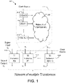
- FIG. 1 is a simplified block diagram illustrating a network system of multiple time-interleaving (TI) instances according to an example of the present invention.
- system 100 includes a plurality of TI instances 110, each of the TI instances receiving one or more clock signals from a clock source.
- the expanded view 111 shows an example configuration of a TI instance 110 having a plurality of clock generation units (CGUs) 120 coupled to a network of interleavers 130. Each of these CGUs receive one or more clock signals from the clock source and provides a certain clock signal of a designated frequency to the interleaver network 130.
- CGUs clock generation units
- System 100 can be a typical multi-TI system having a large-scale network of H TI instances, each of which by itself can be another large-scale network or, at the lowest level, an N-layer interleaving system, a network of many interleaving elements (as shown in view 111), or the like.
- these TI instances operate on the same beat or fundamental frequency, even though the actual source clocks may physically be common or different.
- This large-scale network can be configured to process a set of input signal tensors x 0 ...x H-1 of arbitrary dimensions and to produce a corresponding set of output signal tensors y 0 ...y H-1 , also of arbitrary dimensions.
- These signal tensors can be used for many applications, such as signal processing, data analysis, machine learning, and the like.
- the plurality of CGUs can be configured to generate the necessary phases for all its sub-elements or lower level interleavers of the interleaver network 130.
- Examples of such CGUs include but are not limited to crystal oscillators, phase-locked loop (PLL), and CMOS dividers used in integrated circuits.
- PLL phase-locked loop
- CMOS dividers used in integrated circuits.
- Figure 2A is a simplified graph illustrating misaligned signals in a multiple-TI instance network.
- graph 201 shows a plurality of 1-dimensional sinusoidal outputs that are misaligned, representing misaligned output signal tensors of a multiple interleaving instance system.
- Figure 2B is a simplified graph illustrating aligned signals in a multiple-TI instance according to an example of the present invention.
- graph 202 shows the same plurality of 1 -dimensional sinusoidal outputs now aligned.
- TI system instances In commercial applications, we often have more than one TI system instances operating in parallel with each other (see Figure 1 ). In such scenarios, these TI system instances may have different phases that may be misaligned due to the random starting states of various dividers throughout the clock tree. As a result, the outputs of these instances may be misaligned when interfacing with the external world (see Figure 2A ), which is undesirable.
- the present invention provides for using alignment via detection, alignment via statistical correlation, and the like and combinations thereof.
- a method of operating a multiple instance TI system (or multi-instance TI system) using alignment via detection is briefly described as follows:
- the present invention provides a multi-instance TI system having a phase detector and a plurality of TI devices.
- Each of the TI devices includes a plurality of dividers, and the phase detector is configured to determine the phase difference between the divider output clocks of a designated reference TI device and those of the remaining TI devices of the multi-instance TI system.
- each of the TI devices can include a multiplexer or each of the TI devices can be coupled to a multiplexer stage having a plurality of multiplexers coupled to each of the TI devices.
- the phase detector is configured to compare divider output clocks of the reference TI device to the divider output clocks of each other TI device, progressing from the highest-level divider to the lowest-level divider, one level at a time.
- These divider output clocks are sent to a common sense point (e.g., the phase detector, a buffer stage prior to the phase detector, or the like) using multiplexers.
- a common sense point e.g., the phase detector, a buffer stage prior to the phase detector, or the like
- each of the dividers of the other TI devices can be compared to each of the dividers of the reference TI device, from the highest to lowest, in a round-robin fashion.
- the comparison order can also be performed in other fashions, such as lowest to highest, or as a binary grouped tree, and the like (instead of round-robin) to reduce the number of comparisons.
- these choices come with certain restrictions of the types of dividers that normally increase implementation cost and complexity.
- use of the round-robin comparison process is merely an example of this invention due to its simplicity and wide applicability.
- each TI device includes a divide-by-4 (Div-4) and a divide-by-8 (Div-8) dividers and is configured to receive four input clock phases and to produce 128 output clock phases.
- the system can have one TI device that is misaligned to another TI device from random starting points of itsDiv-4) and Div-8 dividers.
- the present invention provides for a method of aligning these two dividers starting from the highest-level divider Div-4 and progressing downward through the interleaving tree towards the lowest-level divider Div-8. Further details are discussed in reference to Figure 3 .
- FIG. 3 is a simplified block diagram illustrating a multiple TI instance system 300 configured to align the outputs of a plurality of TI devices (i.e., TI system instances) using a phase detector according to an example of the present invention.
- device 300 includes a phase detector 310 coupled to a plurality of TI devices 320 via a plurality of multiplexers 330.
- the multiplexers 330 can be configured within each TI device 320 (as shown) or separate from the TI devices 320.
- each TI device 320 is a 2-layer 4-16-8 TI system, including a Div-4 divider 340 and a Div-8 divider 350.
- the TI devices 320 can be different multi-layer TI devices, such as a 3-layer TI system or a TI system having more layers/dimensions.
- one of the TI devices 320 is designated as the reference (marked by dotted region 321), and all other branches are aligned to the reference branch in a round-robin fashion, or in other fashions as discussed previously.
- the phase detector is configured to determine the difference in phase between the reference TI device and each of the other TI devices.
- the reference divider outputs of the reference TI device are compared to the corresponding target divider outputs of a target TI device.
- the dividers of the reference and target TI devices are compared sequentially from the highest-level divider to the lowest-level divider. Referring to Figure 3 , an example of this process with the 4-16-8 TI devices is first comparing and aligning the Div-4 (i.e., the highest-level divider) of the reference and a target TI device, then comparing and aligning the Div-8 (i.e., the lowest-level divider) of the reference and the target TI device. As discussed previously, all target TI devices can be compared and aligned to the reference TI device in a round-robin fashion, or in other fashions. Those of ordinary skill in the art will recognize other variations, modifications, and alternatives.
- phase detection device such as an XOR/XNOR gate type phase detector
- converter such as Time-to-Digital Converter (TDC) device
- TDC Time-to-Digital Converter
- Figure 4A is a simplified circuit diagram 401 illustrating an XOR/XNOR gate phase detection device for comparing outputs according to an example of the present invention.
- device 2001 includes an XNOR gate 410 configured to receive and compare a reference clock signal (REF) and a target clock signal (CLK).
- the XNOR gate 410 generates the phase difference between the REF and CLK signals and outputs the difference to a low-pass filter 420 to convert this time difference to the voltage domain.
- REF reference clock signal
- CLK target clock signal
- the low-pass filter 420 includes a resistor 421 and capacitor 422 in a RC low-pass filter configuration.
- voltage divider stage 430 including a first resistor 431 coupled to a voltage source (Vdd) and a second resistor 432 coupled to ground.
- the voltage divider stage also includes a transistor 440 configured as a voltage-controlled resistor receiving a bias voltage (BIAS).
- the low-pass filter 420 is configured to convert the time difference between the REF and CLK signals to the voltage domain, which is then measured by an analog-to-digital converter (ADC) 450 coupled to the output of the low-pass filter 2020.
- ADC analog-to-digital converter
- the phase of the dividers producing the CLK signals can be adjusted to be aligned to the dividers producing the REF signals by using retimers or a state machine implemented by a digital signal processor.
- FIG 4B is a simplified timing diagram 402 illustrating the operating of the XOR/XNOR gate architecture as shown in Figure 4A .
- timing diagram 402 shows a reference clock and a plurality of target clocks having a total of N states.
- the reference clock signal can represent the output of a divider of the reference TI device 421 shown in Figure 3 .
- the plurality of target clocks can represent the rest of the plurality of outputs corresponding to the divider of the target TI devices 320 (i.e., all other TI devices in the multiple TI instance system) that will be aligned to the divider of the reference TI device 321.
- FIG. 5 is a simplified timing diagram 500 illustrating a method of applying the phase detector device 401 of Figure 4A to the multiple TI instance device 300 of Figure 3 according to an example of the present invention.
- timing diagram 500 shows the outputs for the reference clock, the target clocks, and a filter settled output of the XNOR gate 410 of the phase detector device 401.
- the target clock signals of the Div-4 divider 340 have four different states, which produces three possible voltages when fed to the XNOR gate 410 due to how well-matched or mismatched the two input phases are.
- a simple 2-bit ADC can detect the highest or lowest value, signifying that the two input divider states (reference and target) are either perfectly aligned or misaligned.
- the phase detector device 401 cycles through the target divider output (i.e., target clock) states, the history of the divider state will repeat, which can serve as another metric indicating how far or close the different dividers are at alignment.
- the phase detector device 401 will detect five possible voltage levels due to how well-matched or mismatched the two input phases are.
- phase detection for a divider producing N states i.e., Div-N
- the more levels that the phase detector needs to detect the finer the resolution is required of the detection ADC.
- the ADC must have a resolution and range that is better than the N/2 +1 voltage levels that it is trying to detect.
- phase detection device can achieve similar performance using an XOR gate configured to receive and compare the reference and target clock signals and feeding the output to a high-pass filter.
- an XOR gate configured to receive and compare the reference and target clock signals and feeding the output to a high-pass filter.
- FIG. 6A is a simplified circuit block diagram illustrating a TDC-based phase detector device 601 according to an example of the present invention.
- device 601 includes a plurality of flip-flops 610 configured as a flip-flop chain that receives a first input clock signal (denoted as "H") and a plurality of buffer devices 620 configured as a buffer delay chain that receives a second input clock signal (denoted as "V").
- the V signal is used to generate a time grid via the buffer delay chain, while the H signal is sampled by the flip-flop chain for comparison against the time-grid. Any two clock signals can be the H and V signals in this TDC method.
- the TDC device 601 is configured to generate a plurality of delay cell outputs from the plurality of buffer devices 620 using the V clock signal.
- This plurality of delay cell outputs that serves as a time grid that moves as one steps through the different states of the V clock.
- the plurality of flip-flops 610 e.g., D flip flops or the like
- the plurality of flip-flops 610 is configured to receive the H clock signal and to compare the H signal to the time grid to determine the phase/alignment difference between the H and V clock signals.
- the H clock signal received by the plurality of flip-flops 610 is sampled and retimed using the time-grid, shown by the clock inputs of the flip-flops 610 being coupled to the staggered outputs of the buffer devices 610.
- the number of buffer devices and flip-flops are both determined by the total number of clock signals in each of the TI devices in the multiple TI instance system.
- the time-grid represents either the current TDC output or the history of the TDC output to be used to determine alignment states.
- a clock buffer device can be used to provide the H and V clock signals to the TDC device 601.
- the clock buffer device can be configured to buffer a reference clock signal (REF) and a target clock signal (CLK) prior to TDC device 601 and send the REF and CLK signals in either order to the TDC device 601.
- the clock buffer device can include a delay chain having a plurality of inverters for each of the REF and CLK signals. An inverter in each delay chain can be configured with resistive feedback.
- the inputs to the clock buffer device can have coupling capacitors. There can be other variations, modifications, and alternatives.
- FIG. 6B is a simplified timing diagram 602 illustrating a method of using a TDC based phase detector device according to an example of the present invention.
- Timing diagram 602 shows how one clock input is used to generate a time grid via a delay chain, and this time grid is then used to sample the other clock via a chain of flip flops.
- the TDC output is either all zeroes or all ones (these values may be skipped until a transition occurs).
- perfect alignment occurs at the moment the TDC outputs change from all zeroes to all ones (or vice versa).
- a "key transition state” i.e., a mix of ones and zeroes
- the "aligned state” is the state that immediately follows this "key transition state”.
- the history of the TDC output or the TDC output itself can be used to determine alignment states.
- requirements of the TDC can include that (1) the TDC must be less noisy than the smallest UI that it attempts to detect, and (2) the TDC length must be larger than 50% of the lowest frequency clock period by a sufficient margin such that the TDC does not get confused between states that are immediately adjacent to perfect alignment.
- FIG. 6C is a simplified timing diagram 603 illustrating a method of using a TDC based phase detector device according to an example of the present invention.
- timing diagram 603 shows N target clock signals that are being evaluated by the TDC based phase detector device.
- an equivalent time grid is shown representing the time grids for each of the target clocks to be aligned to the reference clock.
- phase detection methodologies described above can be used in combination with each other or with another similar method for redundancy in detection accuracy.
- both the XOR/XNOR gate phase detector and the TDC phase detector can be configured together via one or more multiplexers, which allows the system to select between the modes.
- multiplexers which allows the system to select between the modes.
- the present invention also provides for using various statistical correlation-based device architectures, including auto-correlation using a pre-deterministic input signal pattern, pre-deterministic alternating state patterns, or multiple pre-deterministic patterns, or the like and combinations thereof.
- system inputs or states can be controlled, (such as analog-to-digital, digital-to-analog, any neural network, or the like)
- the signals going through the interleaving network can be altered (e.g., using a hardware implementation, firmware, a microprocessor, a microcontroller, or other embedded processing unit or the like) to create certain effects that can reveal the phase differences or internal clock stages.
- Any of the following topologies can be implemented to align a plurality of interleaving sub-systems of a multi-instance interleaving network system.
- FIG. 7 is a simplified block diagram illustrating a multiple TI instance network using auto-correlation according to an example of the present invention.
- system 700 includes a plurality of TI instances 710 coupled to an auto-correlation device 720.
- One of the instances can be designated as a reference instance (marked by dotted lines).
- a pre-deterministic input pattern with a period larger than the period of the respective interleaved clock is fed to different TI instances 710 (through the interleaver network) and the auto-correlation of the resulting outputs is used to detect alignment. Alignment is achieved when output of the auto-correlation device 720 exhibits a maximum correlation value.
- the requirements for this method and device topology can include the following: (1) the ability the switch the input data going into the TI system to a predetermined pattern on all TI instances to be aligned; (2) the pattern period is longer than the target clock period to be aligned, and (3) the auto-correlation output at max alignment is sufficiently higher than that of adjacent near-alignment states beyond the sum of all noise sources.
- a common pseudorandom binary sequence (PRBS) or sinusoidal input can be fed into the system 700 shown in Figure 7 .
- PRBS pseudorandom binary sequence
- instance #1 as its clock is forced through different states (e.g., via internal phase control, retimers, finite state machine, etc.) and auto-correlation device 720 measures the correlation between its output (i.e., auto-correlation output of instance #1) and that of instance #0 (i.e., reference instance), a certain pattern emerges that looks similar to Figures 8A and 8B .
- the maximum value of correlation occurs only when the two outputs are perfectly aligned, whether with a PRBS, ramp, periodic ramp, alternating periodic ramp, stair-case, spike, periodic spike, alternating periodic spike, sinusoidal, or other signal excitation.
- the alignment algorithm can keep stepping instance #1's clock state until this value is reached and subsequently proceed to the rest of the instances until all instances are similarly aligned to instance #0. Similar to the XOR/XNOR phase detector case, alignment via auto-correlation can be done in a round-robin fashion, or any other order depending upon the application.
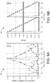
- Figure 8A is a simplified graph of normalized correlation outputs illustrating a method of auto-correlation using a common PRBS input signal and a sinusoidal input signal in a multi-instance TI system according to an example of the present invention.
- graph 801 illustrates the further a TI instance is away from a phase offset value of zero (i.e., perfect alignment), the closer the normalized correlation output is to one.
- This graph 801 shows a normalized version of the detection threshold graph 802 in Figure 8B .
- Figure 8B is a simplified graph of detection thresholds illustrating a method of auto-correlation using a common PRBS input signal and a sinusoidal input signal in a multi-instance TI system according to an example of the present invention.
- graph 802 illustrates that the further a TI instance is away from a phase offset value of zero (i.e., perfect alignment), the smaller the correlation output.
- the difference in correlation value between perfect alignment and other non-aligned states is referred to as the "detection threshold", which is plotted against actual phase offset.
- the internal states/bias points of the IT instances can be varied in a distinct and alternating state signature (e.g., between its normal and opposite state).
- the internal states of the IT instances can be modulated based on different variables (i.e., internal state variables), such as offset, gain, distortion properties, magnitude properties, and the like.
- the average autocorrelation of these alternating states over time creates a sufficiently distinct signature in the final output when their clocks are out of phase. Perfect alignment is achieved when the correlation value is maximized.
- the autocorrelation between any pair of types reduce to zero, since they are statistically independent processes.
- auto-correlating two output patterns will reduce to a statistically constant bias term B that is proportional to the signal and noise energy plus a varying term ⁇ ik that depends on the position of the offset pattern.
- this offset pattern is shifted around.
- corresponding state terms for alternating gain states would include g ⁇ i [ t ] and g ⁇ k [ t ] as the i-th and k-th instance gain and G ⁇ ik [ t ] as the auto-correlation of the i-th and k-th instance as the result of gain variation.
- Figure 9A is a simplified graph of normalized correlation outputs illustrating a method of auto-correlation using different offset patterns in a multi-instance TI system according to an example of the present invention.
- graph 901 has three patterns plotted for demonstration: (1) no pattern; (2) periodic spike; and (3) periodic ramp. Similar to graph 801 of Figure 8 , graph 901 is a normalized version of the offset graph 902 in Figure 9B .
- Figure 9B is a simplified graph of detection thresholds illustrating a method of auto-correlation using different offset patterns in a multi-instance TI system according to an example of the present invention.
- graph 902 shows the average autocorrelation over time vs. interleaving phase offset of the three offset patterns discussed previously.
- the autocorrelation peak can be easily detected when perfect alignment occurs, demonstrating the effectiveness of this topology.
- an advantage of this topology of the previous topology is that it does not require switching the input to a pre-determined pattern, which can be a difficult requirement in certain applications.
- this algorithm work and depending on the specific applications, some or all of the following conditions must be satisfied.
- the requirements for the method and device topology can include the following: (1) the offset altering pattern must be the same (or sufficiently close enough) for all interleaving instances to allow for detectable autocorrelation of differences between adjacent states near the zero offset state; (2) the offset pattern fed to the interleavers have signal energy sufficiently greater than the total noise of the system; (3) the autocorrelation window (over which the above equation is computed) is sufficiently long to average out all noise effects and the effect of the offset pattern alternation; and (4) in certain applications, use of these alternating offset patterns across two or more interleaving instances must happen simultaneously( or at least concurrently close enough in time) such that the relative time errors of such offset applications do not result in larger than one phase offset sample in the final autocorrelation output.
- the inverse is also application in systems where opposite alignment is needed or if a TI instance's output sign is flipped. Regardless of the scenarios, the methods and topologies presently described should provide sufficient granularity or resolution in the final phase detection such that almost any desired discrete phase relationship can be targeted for alignment.
Landscapes
- Engineering & Computer Science (AREA)
- Theoretical Computer Science (AREA)
- Computer Networks & Wireless Communication (AREA)
- Signal Processing (AREA)
- Physics & Mathematics (AREA)
- Nonlinear Science (AREA)
- Manipulation Of Pulses (AREA)
Applications Claiming Priority (1)
| Application Number | Priority Date | Filing Date | Title |
|---|---|---|---|
| US17/183,919 US11309904B1 (en) | 2021-02-24 | 2021-02-24 | Method and device for synchronization of large-scale systems with multiple time interleaving sub-systems |
Publications (2)
| Publication Number | Publication Date |
|---|---|
| EP4050801A1 true EP4050801A1 (de) | 2022-08-31 |
| EP4050801B1 EP4050801B1 (de) | 2025-12-31 |
Family
ID=80785000
Family Applications (1)
| Application Number | Title | Priority Date | Filing Date |
|---|---|---|---|
| EP22157992.3A Active EP4050801B1 (de) | 2021-02-24 | 2022-02-22 | Verfahren und vorrichtung zur synchronisation von grosssystemen mit mehreren zeitverschachtelten untersystemen |
Country Status (3)
| Country | Link |
|---|---|
| US (2) | US11309904B1 (de) |
| EP (1) | EP4050801B1 (de) |
| CN (1) | CN114978393A (de) |
Families Citing this family (2)
| Publication number | Priority date | Publication date | Assignee | Title |
|---|---|---|---|---|
| US11750166B2 (en) | 2021-01-13 | 2023-09-05 | Marvell Asia Pte. Ltd. | Method and device for high bandwidth receiver for high baud-rate communications |
| US11309904B1 (en) | 2021-02-24 | 2022-04-19 | Marvell Asia Pte Ltd. | Method and device for synchronization of large-scale systems with multiple time interleaving sub-systems |
Citations (3)
| Publication number | Priority date | Publication date | Assignee | Title |
|---|---|---|---|---|
| US20100153041A1 (en) * | 2007-06-04 | 2010-06-17 | Nxp B.V. | Error processing in time interleaved signal processing devices |
| US20140232575A1 (en) * | 2013-02-20 | 2014-08-21 | Stmicroelectronics Sa | Method and Device for use with Analog to Digital Converter |
| US20150070065A1 (en) * | 2013-09-12 | 2015-03-12 | Fujitsu Semiconductor Limited | Signal-alignment circuitry and methods |
Family Cites Families (36)
| Publication number | Priority date | Publication date | Assignee | Title |
|---|---|---|---|---|
| US6118438A (en) | 1997-03-18 | 2000-09-12 | Ati Technologies, Inc. | Low comment mode impedence differential driver and applications thereof |
| US5977796A (en) | 1997-06-26 | 1999-11-02 | Lucent Technologies, Inc. | Low voltage differential swing interconnect buffer circuit |
| US6111431A (en) | 1998-05-14 | 2000-08-29 | National Semiconductor Corporation | LVDS driver for backplane applications |
| JP3171175B2 (ja) | 1998-12-08 | 2001-05-28 | 日本電気株式会社 | 差動トライステート発生方法及び差動トライステート回路 |
| US6417708B1 (en) | 2000-10-02 | 2002-07-09 | Lsi Logic Corporation | Resistively-loaded current-mode output buffer with slew rate control |
| US6552582B1 (en) | 2001-09-27 | 2003-04-22 | Applied Micro Circuits Corporation | Source follower for low voltage differential signaling |
| US6686772B2 (en) | 2001-11-19 | 2004-02-03 | Broadcom Corporation | Voltage mode differential driver and method |
| US7265433B2 (en) | 2005-01-13 | 2007-09-04 | International Business Machines Corporation | On-pad broadband matching network |
| WO2006117860A1 (ja) | 2005-04-28 | 2006-11-09 | Thine Electronics, Inc. | 差動駆動回路およびそれを内蔵する電子機器 |
| GB0702590D0 (en) | 2007-02-09 | 2007-03-21 | Texas Instruments Ltd | A clock circuit |
| JP2009159296A (ja) | 2007-12-26 | 2009-07-16 | Panasonic Corp | クロック信号生成装置及び方法 |
| US8022729B2 (en) | 2008-04-11 | 2011-09-20 | Micron Technology, Inc. | Signal driver circuit having adjustable output voltage for a high logic level output signal |
| US7714617B2 (en) | 2008-09-11 | 2010-05-11 | Micron Technology, Inc. | Signal driver circuit having an adjustable output voltage |
| US7728753B2 (en) * | 2008-10-13 | 2010-06-01 | National Semiconductor Corporation | Continuous synchronization for multiple ADCs |
| US8086208B2 (en) | 2008-12-05 | 2011-12-27 | Passif Semiconductor Corp. | Passive wireless receiver |
| US8638130B1 (en) | 2010-02-17 | 2014-01-28 | Entropic Communications, Inc. | Low headroom line driver |
| US8581634B2 (en) | 2010-02-24 | 2013-11-12 | Texas Instruments Incorporated | Source follower input buffer |
| JP5692780B2 (ja) | 2010-10-05 | 2015-04-01 | 日本電気株式会社 | マルチコア型誤り訂正処理システムおよび誤り訂正処理装置 |
| US9496840B2 (en) | 2014-05-16 | 2016-11-15 | Linear Technology Corporation | Radio receiver |
| WO2016029058A1 (en) | 2014-08-20 | 2016-02-25 | Zaretsky, Howard | Fractional-n frequency synthesizer incorporating cyclic digital-to-time and time -to-digital circuit pair |
| US9219490B1 (en) | 2014-09-08 | 2015-12-22 | Lockheed Martin Corporation | Front end sample and hold circuit for a reconfigurable analog-to-digital converter |
| US9432000B1 (en) | 2015-02-04 | 2016-08-30 | Inphi Corporation | Low power buffer with gain boost |
| US10545205B2 (en) | 2017-03-27 | 2020-01-28 | Waveguide Corporation | Voltage-mode passive mixer with integrated input and output buffers |
| US10374838B2 (en) | 2017-06-30 | 2019-08-06 | Futurewei Technologies, Inc. | Image distortion correction in a wireless terminal |
| US10873336B2 (en) | 2017-10-27 | 2020-12-22 | Analog Devices, Inc. | Track and hold circuits for high speed and interleaved ADCs |
| CN109245766B (zh) | 2018-07-20 | 2021-03-30 | 中国电子科技集团公司第二十四研究所 | 一种时间交织结构模数转换器的误差补偿校正系统及方法 |
| US11258431B2 (en) | 2018-08-16 | 2022-02-22 | Intel Corporation | Method and apparatus for implementing a super sample rate oversampling channelizer |
| GB2582784B (en) | 2019-04-02 | 2021-05-19 | Graphcore Ltd | Booting tiles of processing units |
| US11880760B2 (en) | 2019-05-01 | 2024-01-23 | Samsung Electronics Co., Ltd. | Mixed-precision NPU tile with depth-wise convolution |
| US10790845B1 (en) * | 2019-05-31 | 2020-09-29 | The Boeing Company | Clocking circuit and method for time-interleaved analog-to-digital converters |
| US11233521B2 (en) | 2019-07-16 | 2022-01-25 | Uti Limited Partnership | Sub-ranging analog to digital converter |
| US11159133B2 (en) | 2019-12-17 | 2021-10-26 | The Boeing Company | Buffer circuit for radio frequency signals |
| US10873486B1 (en) | 2020-01-23 | 2020-12-22 | Goodix Technology Inc. | Receiver circuits with blocker attenuating RF filter |
| US11157037B1 (en) | 2020-11-13 | 2021-10-26 | Marvell Asia Pte, Ltd. | Method and device for clock generation and synchronization for time interleaved networks |
| US11469709B2 (en) | 2020-12-21 | 2022-10-11 | Intel Corporation | Biasing scheme for constant regulated local oscillator in mm-wave tripler |
| US11309904B1 (en) | 2021-02-24 | 2022-04-19 | Marvell Asia Pte Ltd. | Method and device for synchronization of large-scale systems with multiple time interleaving sub-systems |
-
2021
- 2021-02-24 US US17/183,919 patent/US11309904B1/en active Active
-
2022
- 2022-02-22 EP EP22157992.3A patent/EP4050801B1/de active Active
- 2022-02-23 CN CN202210167762.5A patent/CN114978393A/zh active Pending
- 2022-04-18 US US17/722,749 patent/US11750207B2/en active Active
Patent Citations (3)
| Publication number | Priority date | Publication date | Assignee | Title |
|---|---|---|---|---|
| US20100153041A1 (en) * | 2007-06-04 | 2010-06-17 | Nxp B.V. | Error processing in time interleaved signal processing devices |
| US20140232575A1 (en) * | 2013-02-20 | 2014-08-21 | Stmicroelectronics Sa | Method and Device for use with Analog to Digital Converter |
| US20150070065A1 (en) * | 2013-09-12 | 2015-03-12 | Fujitsu Semiconductor Limited | Signal-alignment circuitry and methods |
Non-Patent Citations (3)
| Title |
|---|
| ATHREYA SHANKARRAM ET AL: "Clock Synchronous Reset and Skew Calibration of 65GS/s ADCs in A Multi-Lane Coherent Receiver", ESSCIRC 2018 - IEEE 44TH EUROPEAN SOLID STATE CIRCUITS CONFERENCE (ESSCIRC), IEEE, 3 September 2018 (2018-09-03), pages 250 - 253, XP033420659, [retrieved on 20181016], DOI: 10.1109/ESSCIRC.2018.8494254 * |
| LINGLI XIA ET AL: "Sub-2-ps, Static Phase Error Calibration Technique Incorporating Measurement Uncertainty Cancellation for Multi-Gigahertz Time-Interleaved T/H Circuits", IEEE TRANSACTIONS ON CIRCUITS AND SYSTEMS I: REGULAR PAPERS, IEEE, US, vol. 59, no. 2, 1 February 2012 (2012-02-01), pages 276 - 284, XP011394661, ISSN: 1549-8328, DOI: 10.1109/TCSI.2011.2162382 * |
| LUCA VERCESI ET AL: "Two-Dimensions Vernier Time-to-Digital Converter", IEEE JOURNAL OF SOLID-STATE CIRCUITS, IEEE, USA, vol. 45, no. 8, 1 August 2010 (2010-08-01), pages 1504 - 1512, XP011314246, ISSN: 0018-9200, DOI: 10.1109/JSSC.2010.2047435 * |
Also Published As
| Publication number | Publication date |
|---|---|
| CN114978393A (zh) | 2022-08-30 |
| US11309904B1 (en) | 2022-04-19 |
| US20220271766A1 (en) | 2022-08-25 |
| EP4050801B1 (de) | 2025-12-31 |
| US11750207B2 (en) | 2023-09-05 |
Similar Documents
| Publication | Publication Date | Title |
|---|---|---|
| KR100847213B1 (ko) | 난수 생성 방법 및 난수 생성기 | |
| US8468186B2 (en) | Combination of values from a pseudo-random source | |
| EP4050801A1 (de) | Verfahren und vorrichtung zur synchronisation von grosssystemen mit mehreren zeitverschachtelten untersystemen | |
| JP6594420B2 (ja) | 時間デジタル変換器およびデジタル位相同期ループ | |
| US9166770B2 (en) | Clock-generating device and clock data recovery device | |
| JP2007235908A (ja) | リング発振回路、遅延時間測定回路、テスト回路、クロック発生回路、イメージセンサ、パルス発生回路、半導体集積回路、及び、そのテスト方法 | |
| JP2002281007A (ja) | 信号発生回路、クロック復元回路、検証回路、データ同期回路およびデータ復元回路 | |
| US12267081B2 (en) | Apparatus for digital representation of angular difference | |
| US11507129B2 (en) | Method and device for clock generation and synchronization for time interleaved networks | |
| US11271550B1 (en) | Synchronous divider based on cascaded retiming | |
| JP6550502B1 (ja) | 固有データ生成装置、半導体装置および認証システム | |
| US7424081B2 (en) | Semiconductor integrated circuit device | |
| CN104579320A (zh) | 时钟延迟方法、装置、延迟锁相环及数字时钟管理单元 | |
| Wang et al. | A 10.8-to-37.4 Gb/s reference-less FD-less single-loop quarter-rate bang-bang clock and data recovery employing deliberate-current-mismatch wide-frequency-acquisition technique | |
| EP1518164B1 (de) | Verfahren und vorrichtung zur generierung von zufallszahlen mittels metastabiler flip-flops | |
| US20050004959A1 (en) | VLSI implementation of metastability-based random number generator using delay ladders | |
| Marini et al. | FPGA implementation of an NCO based CDR for the juno front-end electronics | |
| CN115867885B (zh) | 真随机数发生器 | |
| CN116155267A (zh) | 一种延时时长可配置的延时链电路 | |
| JP2002323971A (ja) | 乱数発生装置 | |
| Simka et al. | Model of a true random number generator aimed at cryptographic applications | |
| KR101000486B1 (ko) | 지연고정 루프 기반의 주파수 체배기 | |
| CN113535124B (zh) | 基于片上数字反馈自校准系统的真随机数发生器 | |
| JP2002182779A (ja) | 変更されたクロック信号発生器 | |
| US20070200641A1 (en) | System and method for multiple-phase clock generation |
Legal Events
| Date | Code | Title | Description |
|---|---|---|---|
| PUAI | Public reference made under article 153(3) epc to a published international application that has entered the european phase |
Free format text: ORIGINAL CODE: 0009012 |
|
| STAA | Information on the status of an ep patent application or granted ep patent |
Free format text: STATUS: THE APPLICATION HAS BEEN PUBLISHED |
|
| AK | Designated contracting states |
Kind code of ref document: A1 Designated state(s): AL AT BE BG CH CY CZ DE DK EE ES FI FR GB GR HR HU IE IS IT LI LT LU LV MC MK MT NL NO PL PT RO RS SE SI SK SM TR |
|
| STAA | Information on the status of an ep patent application or granted ep patent |
Free format text: STATUS: REQUEST FOR EXAMINATION WAS MADE |
|
| 17P | Request for examination filed |
Effective date: 20230227 |
|
| RBV | Designated contracting states (corrected) |
Designated state(s): AL AT BE BG CH CY CZ DE DK EE ES FI FR GB GR HR HU IE IS IT LI LT LU LV MC MK MT NL NO PL PT RO RS SE SI SK SM TR |
|
| P01 | Opt-out of the competence of the unified patent court (upc) registered |
Effective date: 20230509 |
|
| GRAP | Despatch of communication of intention to grant a patent |
Free format text: ORIGINAL CODE: EPIDOSNIGR1 |
|
| STAA | Information on the status of an ep patent application or granted ep patent |
Free format text: STATUS: GRANT OF PATENT IS INTENDED |
|
| INTG | Intention to grant announced |
Effective date: 20250829 |
|
| GRAS | Grant fee paid |
Free format text: ORIGINAL CODE: EPIDOSNIGR3 |
|
| GRAA | (expected) grant |
Free format text: ORIGINAL CODE: 0009210 |
|
| STAA | Information on the status of an ep patent application or granted ep patent |
Free format text: STATUS: THE PATENT HAS BEEN GRANTED |
|
| AK | Designated contracting states |
Kind code of ref document: B1 Designated state(s): AL AT BE BG CH CY CZ DE DK EE ES FI FR GB GR HR HU IE IS IT LI LT LU LV MC MK MT NL NO PL PT RO RS SE SI SK SM TR |
|
| REG | Reference to a national code |
Ref country code: CH Ref legal event code: F10 Free format text: ST27 STATUS EVENT CODE: U-0-0-F10-F00 (AS PROVIDED BY THE NATIONAL OFFICE) Effective date: 20251231 Ref country code: GB Ref legal event code: FG4D |
|
| REG | Reference to a national code |
Ref country code: DE Ref legal event code: R096 Ref document number: 602022027692 Country of ref document: DE |
|
| REG | Reference to a national code |
Ref country code: IE Ref legal event code: FG4D |
|
| PGFP | Annual fee paid to national office [announced via postgrant information from national office to epo] |
Ref country code: GB Payment date: 20260223 Year of fee payment: 5 |
|
| REG | Reference to a national code |
Ref country code: LT Ref legal event code: MG9D |
|
| PG25 | Lapsed in a contracting state [announced via postgrant information from national office to epo] |
Ref country code: NO Free format text: LAPSE BECAUSE OF FAILURE TO SUBMIT A TRANSLATION OF THE DESCRIPTION OR TO PAY THE FEE WITHIN THE PRESCRIBED TIME-LIMIT Effective date: 20260331 |
|
| PGFP | Annual fee paid to national office [announced via postgrant information from national office to epo] |
Ref country code: DE Payment date: 20260220 Year of fee payment: 5 |
|
| PG25 | Lapsed in a contracting state [announced via postgrant information from national office to epo] |
Ref country code: HR Free format text: LAPSE BECAUSE OF FAILURE TO SUBMIT A TRANSLATION OF THE DESCRIPTION OR TO PAY THE FEE WITHIN THE PRESCRIBED TIME-LIMIT Effective date: 20251231 Ref country code: FI Free format text: LAPSE BECAUSE OF FAILURE TO SUBMIT A TRANSLATION OF THE DESCRIPTION OR TO PAY THE FEE WITHIN THE PRESCRIBED TIME-LIMIT Effective date: 20251231 |
|
| PGFP | Annual fee paid to national office [announced via postgrant information from national office to epo] |
Ref country code: AT Payment date: 20260301 Year of fee payment: 5 |
|
| PG25 | Lapsed in a contracting state [announced via postgrant information from national office to epo] |
Ref country code: RS Free format text: LAPSE BECAUSE OF FAILURE TO SUBMIT A TRANSLATION OF THE DESCRIPTION OR TO PAY THE FEE WITHIN THE PRESCRIBED TIME-LIMIT Effective date: 20260331 |
|
| PGFP | Annual fee paid to national office [announced via postgrant information from national office to epo] |
Ref country code: FR Payment date: 20260224 Year of fee payment: 5 |
|
| PG25 | Lapsed in a contracting state [announced via postgrant information from national office to epo] |
Ref country code: LV Free format text: LAPSE BECAUSE OF FAILURE TO SUBMIT A TRANSLATION OF THE DESCRIPTION OR TO PAY THE FEE WITHIN THE PRESCRIBED TIME-LIMIT Effective date: 20251231 |