EP4047759B1 - Laserverbindungsmodul - Google Patents
Laserverbindungsmodul Download PDFInfo
- Publication number
- EP4047759B1 EP4047759B1 EP19949162.2A EP19949162A EP4047759B1 EP 4047759 B1 EP4047759 B1 EP 4047759B1 EP 19949162 A EP19949162 A EP 19949162A EP 4047759 B1 EP4047759 B1 EP 4047759B1
- Authority
- EP
- European Patent Office
- Prior art keywords
- electrodes
- module
- laser
- parts
- laser diodes
- Prior art date
- Legal status (The legal status is an assumption and is not a legal conclusion. Google has not performed a legal analysis and makes no representation as to the accuracy of the status listed.)
- Active
Links
Images

Classifications
-
- H—ELECTRICITY
- H01—ELECTRIC ELEMENTS
- H01S—DEVICES USING THE PROCESS OF LIGHT AMPLIFICATION BY STIMULATED EMISSION OF RADIATION [LASER] TO AMPLIFY OR GENERATE LIGHT; DEVICES USING STIMULATED EMISSION OF ELECTROMAGNETIC RADIATION IN WAVE RANGES OTHER THAN OPTICAL
- H01S5/00—Semiconductor lasers
- H01S5/02—Structural details or components not essential to laser action
- H01S5/022—Mountings; Housings
-
- F—MECHANICAL ENGINEERING; LIGHTING; HEATING; WEAPONS; BLASTING
- F16—ENGINEERING ELEMENTS AND UNITS; GENERAL MEASURES FOR PRODUCING AND MAINTAINING EFFECTIVE FUNCTIONING OF MACHINES OR INSTALLATIONS; THERMAL INSULATION IN GENERAL
- F16B—DEVICES FOR FASTENING OR SECURING CONSTRUCTIONAL ELEMENTS OR MACHINE PARTS TOGETHER, e.g. NAILS, BOLTS, CIRCLIPS, CLAMPS, CLIPS OR WEDGES; JOINTS OR JOINTING
- F16B2/00—Friction-grip releasable fastenings
- F16B2/02—Clamps, i.e. with gripping action effected by positive means other than the inherent resistance to deformation of the material of the fastening
- F16B2/06—Clamps, i.e. with gripping action effected by positive means other than the inherent resistance to deformation of the material of the fastening external, i.e. with contracting action
- F16B2/065—Clamps, i.e. with gripping action effected by positive means other than the inherent resistance to deformation of the material of the fastening external, i.e. with contracting action using screw-thread elements
-
- F—MECHANICAL ENGINEERING; LIGHTING; HEATING; WEAPONS; BLASTING
- F16—ENGINEERING ELEMENTS AND UNITS; GENERAL MEASURES FOR PRODUCING AND MAINTAINING EFFECTIVE FUNCTIONING OF MACHINES OR INSTALLATIONS; THERMAL INSULATION IN GENERAL
- F16B—DEVICES FOR FASTENING OR SECURING CONSTRUCTIONAL ELEMENTS OR MACHINE PARTS TOGETHER, e.g. NAILS, BOLTS, CIRCLIPS, CLAMPS, CLIPS OR WEDGES; JOINTS OR JOINTING
- F16B5/00—Joining sheets or plates, e.g. panels, to one another or to strips or bars parallel to them
- F16B5/02—Joining sheets or plates, e.g. panels, to one another or to strips or bars parallel to them by means of fastening members using screw-thread
-
- H—ELECTRICITY
- H01—ELECTRIC ELEMENTS
- H01S—DEVICES USING THE PROCESS OF LIGHT AMPLIFICATION BY STIMULATED EMISSION OF RADIATION [LASER] TO AMPLIFY OR GENERATE LIGHT; DEVICES USING STIMULATED EMISSION OF ELECTROMAGNETIC RADIATION IN WAVE RANGES OTHER THAN OPTICAL
- H01S5/00—Semiconductor lasers
- H01S5/02—Structural details or components not essential to laser action
- H01S5/022—Mountings; Housings
- H01S5/02208—Mountings; Housings characterised by the shape of the housings
-
- H—ELECTRICITY
- H01—ELECTRIC ELEMENTS
- H01S—DEVICES USING THE PROCESS OF LIGHT AMPLIFICATION BY STIMULATED EMISSION OF RADIATION [LASER] TO AMPLIFY OR GENERATE LIGHT; DEVICES USING STIMULATED EMISSION OF ELECTROMAGNETIC RADIATION IN WAVE RANGES OTHER THAN OPTICAL
- H01S5/00—Semiconductor lasers
- H01S5/02—Structural details or components not essential to laser action
- H01S5/022—Mountings; Housings
- H01S5/023—Mount members, e.g. sub-mount members
- H01S5/02315—Support members, e.g. bases or carriers
-
- H—ELECTRICITY
- H01—ELECTRIC ELEMENTS
- H01S—DEVICES USING THE PROCESS OF LIGHT AMPLIFICATION BY STIMULATED EMISSION OF RADIATION [LASER] TO AMPLIFY OR GENERATE LIGHT; DEVICES USING STIMULATED EMISSION OF ELECTROMAGNETIC RADIATION IN WAVE RANGES OTHER THAN OPTICAL
- H01S5/00—Semiconductor lasers
- H01S5/02—Structural details or components not essential to laser action
- H01S5/022—Mountings; Housings
- H01S5/0235—Method for mounting laser chips
- H01S5/02355—Fixing laser chips on mounts
- H01S5/02365—Fixing laser chips on mounts by clamping
-
- H—ELECTRICITY
- H01—ELECTRIC ELEMENTS
- H01S—DEVICES USING THE PROCESS OF LIGHT AMPLIFICATION BY STIMULATED EMISSION OF RADIATION [LASER] TO AMPLIFY OR GENERATE LIGHT; DEVICES USING STIMULATED EMISSION OF ELECTROMAGNETIC RADIATION IN WAVE RANGES OTHER THAN OPTICAL
- H01S5/00—Semiconductor lasers
- H01S5/02—Structural details or components not essential to laser action
- H01S5/024—Arrangements for thermal management
- H01S5/02407—Active cooling, e.g. the laser temperature is controlled by a thermo-electric cooler or water cooling
- H01S5/02423—Liquid cooling, e.g. a liquid cools a mount of the laser
-
- H—ELECTRICITY
- H01—ELECTRIC ELEMENTS
- H01S—DEVICES USING THE PROCESS OF LIGHT AMPLIFICATION BY STIMULATED EMISSION OF RADIATION [LASER] TO AMPLIFY OR GENERATE LIGHT; DEVICES USING STIMULATED EMISSION OF ELECTROMAGNETIC RADIATION IN WAVE RANGES OTHER THAN OPTICAL
- H01S5/00—Semiconductor lasers
- H01S5/40—Arrangement of two or more semiconductor lasers, not provided for in groups H01S5/02 - H01S5/30
- H01S5/4018—Lasers electrically in series
-
- H—ELECTRICITY
- H01—ELECTRIC ELEMENTS
- H01S—DEVICES USING THE PROCESS OF LIGHT AMPLIFICATION BY STIMULATED EMISSION OF RADIATION [LASER] TO AMPLIFY OR GENERATE LIGHT; DEVICES USING STIMULATED EMISSION OF ELECTROMAGNETIC RADIATION IN WAVE RANGES OTHER THAN OPTICAL
- H01S5/00—Semiconductor lasers
- H01S5/40—Arrangement of two or more semiconductor lasers, not provided for in groups H01S5/02 - H01S5/30
- H01S5/4025—Array arrangements, e.g. constituted by discrete laser diodes or laser bar
- H01S5/4031—Edge-emitting structures
- H01S5/4043—Edge-emitting structures with vertically stacked active layers
- H01S5/405—Two-dimensional arrays
Definitions
- the invention refers to a laser connection module providing structural and constitutive characteristics, which will be described in detail below, that significantly improve the current state of the art within their field of application.
- the object of the invention focuses on a module of the type intended to serve as a fastening device for the electrical connection and thermal contact between laser diodes and electrodes stacked successively between corresponding spacers, being able to have internal conduits for the circulation of a cooling fluid, with the advantage of having an improved structural configuration that allows, on the one hand, the fastening and keeping together of all its components, and on the other hand, so as to ensure that such electrical connection is secure, the controlled application of the clamping force directly on the laser diodes and at the point where they meet to ensure electrical and thermal contact between the electrodes and diodes.
- the laser diodes also called chips or bars, were mounted on at least one of the electrodes by means of welding, which poses several problems.
- the main problem is that the laser chip must be positioned with extreme precision, so that its end protrudes between eight and ten microns from the end of the electrode so that the welded connection that will join it to said electrode does not reach the epitaxy, because if it does, the laser module will be faulty.
- the welded connection of the laser chip does not allow subsequent adjustment of its position or its replacement in case of failure.
- Patent Document US5978396 describes a semiconductor laser source including a stack of semiconductor laser diodes, each having at least one active region.
- the active region includes a series of semiconductor layers located between an ohmic contact layer and a substrate, which also assumes the function of an ohmic contact layer. Pressure causes the diodes to maintain contact with each other through their ohmic contact layers.
- Each diode has dimensions, especially in its thickness, that allow the transient heating of each diode to be as low as possible and such that the average heating of the stackable diodes does not exceed a predetermined value.
- Patent Document US6151341 describes a stackable integrated diode pack, wherein a stack of laser elements, configured to absorb the heat given off by said laser elements, is proposed to allow for their repair and/or replacement, and testing.
- the assembly comprises cells which have a cavity for the passage of a coolant to cool the laser elements.
- the cells can be individually constructed for individual testing and then stacked together and secured detachably for easy replacement.
- the cell cavities form a substantially contiguous cavity through which the coolant enters and exits the entire assembly.
- the cell cavities include regions and surfaces that enhance coolant flow to regions substantially adjacent to the laser elements, to cool said laser elements.
- Patent Document US6245589 describes the manufacture of a device for cooling a planar light source, which includes a device for cooling an array of laser diodes using a stacking of a plurality of metal plates, formed with a grooved pattern with arms or openings, which act as a cooling water circulation path for said laser diodes.
- Patent Document ES2191559B1 proposes a laser connection module, comprising: - electrodes mutually facing each other and connected in an alternating order with opposite poles; insulating spacers arranged between the facing surfaces of the electrodes to prevent direct contact of the electrodes and their short-circuit; laser chips mounted between the facing surfaces of said electrodes, making contact with the electrodes; - and a clamping means responsible for drawing together the electrodes mutually facing each other to ensure their contact with the laser chips positioned between them, ensuring the electrical power supply to said laser chips and the dissipation of the heat generated.
- the aforementioned clamping means consist of screws mounted on through holes affecting the electrodes and the insulating spacers, and of corresponding nuts which thread on said screws, the heads of the screws and the nuts acting directly on the outer surface of the two electrodes occupying the end positions in the laser module.
- one of the disadvantages is the risk of damage to the end electrodes, due to the screw heads and the respective nuts in the clamping areas acting directly on them, taking into account: on the one hand, that these electrodes are made of a relatively soft electrically conductive material, such as copper and, on the other hand, that the section of the electrodes is reduced in said clamping areas by the holes made for the mounting of the screws.
- Patent Document ES2191559B1 An additional disadvantage of the invention disclosed in Patent Document ES2191559B1 is that the upper and lower end electrodes are exposed, without any element of protection against possible accidental impacts, which increases the risk of damage to the laser module.
- the objective of the invention herein is, therefore, to provide an improved laser module that performs a correct fastening between all the stacked components of the module, protects the end electrodes so that they are not exposed to accidental impacts, and ensures that the screws and nuts of the clamping elements do not act directly on said end electrodes, hence preventing them from being damaged.
- the laser connection module the subject matter of the invention, with the technical characteristics set forth in claim 1, satisfactorily solves the above-mentioned drawbacks.
- the laser connection module of the invention is of the type employed for the electrical connection between laser diodes and alternately stacked electrodes and laser diodes, and can be provided with internal conduits for the circulation of a cooling fluid.
- This laser connection module has technical characteristics that make it possible to fasten all its components and keep them together, and simultaneously provide protection to the end electrodes, preventing them from being damaged due to an accidental impact, or due to the clamping screws and nuts acting directly on said end electrodes; and without said clamping screws going through the electrical power supply electrodes of the laser diodes.
- this laser connection module is of the type described in the preamble of claim 1 comprising: several superimposed electrodes, connected in an alternating order with opposite electrical power supply poles; at least one laser diode mounted between the facing surfaces of consecutive electrodes, making contact with said electrodes; and a means for clamping the assembly of electrodes and laser diodes together.
- this laser connection module comprises:
- Said external structure comprises: an upper part forming the first end of the structure; a lower part forming the second end of the structure and a means for fastening said upper and lower parts in a parallel position, separated vertically at a suitable distance for the unconstricted housing of the electrode and laser diode assembly between said upper and lower parts; so that the clamping means is responsible for pressing the electrode and laser diode assembly against the lower part of the structure.
- the external structure provides adequate protection for the electrode and laser diode assembly, while serving as a support for the clamping means responsible for pressing the electrode and laser diode assembly against the lower part or second end of the structure, without said clamping means passing through or weakening any of the elements of the above-mentioned assembly.
- the clamping means comprises clamping studs mounted in threaded holes defined for this purpose in the upper part or first end of the structure.
- the intermediate plate arranged between the clamping studs and the upper electrode closest to them, is made of a resistant material which is harder than the electrodes, its function being to prevent the clamping studs from damaging the upper electrode during the tightening of said studs.
- the means for fastening the upper and lower parts of the structure can have different configurations, being composed of fastening screws; or of tubular spacers arranged between the upper and lower parts and mounted on the fastening screws; or of guide columns arranged between the upper and lower parts and fastened at their ends to the said upper and lower parts.
- said fastening means guarantees an adequate separation between the upper and lower parts of the structure, for the unconstricted housing of the assembly of electrodes and laser diodes.
- the laser connection module includes a means for aligning the successive electrodes in a vertical direction which, depending on the means for fastening the structure, may consist of pins housed in vertical holes made for this purpose in the successive electrodes, or of the guide columns themselves; in the second case, the electrodes have recesses in their contour that are of a configuration complementary to a portion of the section of the guide columns and suitable for the assembly of the electrodes, as a sliding element, between said guide columns; said guide columns forming simultaneously a means for separating the upper and lower parts of the structure and a means for vertically aligning the electrodes.
- the laser diodes are arranged between some front ends of the electrodes, the module comprising electrically insulating spacers located between rear ends of said consecutive electrodes and of a thickness similar to that of the laser diodes, said spacers preventing the consecutive electrodes from touching each other and causing a short circuit.
- the clamping means comprises front studs that clamp the front end of the electrodes against the laser chips and rear studs that clamp the rear end of the electrodes against the electrically insulating spacers, said front and rear studs compensating the clamping on the respective ends of the electrodes.
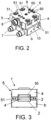
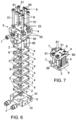
- the laser connection module (1) comprises: electrodes (2) connected in an alternating order with opposite poles of electrical power supply; a spacer (3) arranged between the facing surfaces of the consecutive electrodes (2) to prevent their direct contact and short-circuit, a laser diode (4) mounted between the facing surfaces of consecutive electrodes (2), making contact with them in the area left free by the corresponding spacer (3); and a clamping means (6) for clamping the assembly of electrodes (2) and laser diodes (4) to each other.
- the spacer (3) has a smaller surface than the facing surfaces of the electrodes (2).
- the module (1) comprises an external structure (5) delimiting a space defined by a light emission zone of the laser diode (4) and suitable for housing the electrode assembly (2) and laser diodes (4); the clamping means (6) is mounted on a first end of the structure (5) and presses the assembly of electrodes (2) and laser diodes (4) against a second opposite end of said structure, establishing their fastening and the mutual contact of the laser diodes (4) with the consecutive electrodes (2).
- the module (1) comprises, between the clamping means (6) and the end electrode (2) closest to said clamping means (6), an intermediate plate (50) protecting said end electrode (2).
- the external structure (5) comprises: - an upper part (a) forming the first end of the structure (5) and provided with threaded holes (55) in which studs (60) are mounted forming part of the clamping means (6), - a lower part (b) forming the second end of the structure (5), and - a means for fastening said upper (a) and lower (b) parts in a parallel position, vertically separated at a suitable distance for the unconstricted housing of the electrode and laser diode assembly between said upper and lower parts.
- the means for fastening the upper (a) and lower (b) parts of the external structure (5) comprises fastening screws (51) mounted, with the insertion of washers (54), in through holes (52) defined in the upper part (a) and inserted into threaded holes (53) of the lower part (b), allowing an adjustment of the gap between the upper (a) and lower (b) parts of the external structure (5).
- the module (1) has connectors (7) for a wiring (not shown) of the electrical power supply of the electrodes (2), and internal conduits (10) for the circulation of a cooling product.
- the module (1) includes a means for vertically aligning the successive electrodes (2), consisting of pins (8) housed in vertical holes made for this purpose in the successive electrodes (2) and in the upper (a) and lower (b) parts of the external structure (5); seals (9) are interposed between these elements to prevent leakage.
- the laser diodes (4) are arranged between the front ends of the electrodes (2), and the spacers (3), electrically insulating and of a similar thickness to the laser diodes (4), are arranged between consecutive rear ends of the electrodes (2).
- the clamping means comprises: front studs (60) which press the front end of the electrodes (2) against the laser diodes (4), and rear studs (61) which press the rear end of the electrodes (2) against the electrically insulating spacers (3).
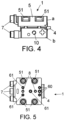
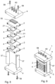
- the laser connection module has a configuration similar to that described above, incorporating in this case a larger number of electrodes (2) and laser diodes (4) stacked in an alternating order.
- the means for fastening the upper (a) and lower (b) parts of the structure (5) comprises tubular spacers (56), arranged between said upper (a) and lower (b) parts and mounted on the fastening screws (51), said tubular spacers (56) being precisely those that determine the separation between the upper (a) and lower (b) parts.
- the means for fastening the upper (a) and lower (b) parts of the structure (5) comprises guide columns (57) arranged between the upper (a) and lower (b) parts, and fastened at their ends by means of screws (58) to said upper and lower parts.
- the electrodes (2) have recesses (21) in their contour, said recesses being of a complementary configuration to a portion of the section of the guide columns (57) and suitable for the mounting of the electrodes (2), as a sliding element, between the guide columns; said guide columns (57) forming simultaneously a means for separating the upper (a) and lower (b) parts of the structure and a means for vertically aligning the electrodes (2).
Landscapes
- Physics & Mathematics (AREA)
- Condensed Matter Physics & Semiconductors (AREA)
- General Physics & Mathematics (AREA)
- Electromagnetism (AREA)
- Optics & Photonics (AREA)
- Engineering & Computer Science (AREA)
- General Engineering & Computer Science (AREA)
- Mechanical Engineering (AREA)
- Semiconductor Lasers (AREA)
- Optical Couplings Of Light Guides (AREA)
- Coupling Device And Connection With Printed Circuit (AREA)
Claims (10)
- Laserverbindungsmodul, das Folgendes umfasst: mehrere übereinander liegende Elektroden (2), die in abwechselnder Reihenfolge mit entgegengesetzten Stromversorgungspolen verbunden sind; mindestens eine Laserdiode (4), die zwischen den einander zugewandten Oberflächen aufeinanderfolgender Elektroden (2) angebracht ist und mit diesen in Kontakt steht; ein Element, um die Anordnung von Elektroden (2) und Laserdioden (4) aneinander zu klemmen; und eine Außenstruktur (5), die einen Raum begrenzt, der durch eine Lichtemissionszone der Laserdioden (4) definiert ist und geeignet ist, die Anordnung von Elektroden (2) und übereinander angeordneten Laserdioden (4) aufzunehmen; dadurch gekennzeichnet, dass das Laserverbindungsmodul Folgendes umfasst:- ein Klemmelement (6), das Bolzen (60) umfasst, die auf Gewindelöchern (55) montiert sind, die an einem ersten Ende der Außenstruktur (5) definiert sind, und das die Anordnung von Elektroden (2) und Laserdioden (4) gegen ein zweites, gegenüberliegendes Ende der Struktur (5) drückt, wodurch ihre Befestigung und der gegenseitige Kontakt der Laserdioden (4) mit den aufeinanderfolgenden Elektroden (2) hergestellt wird, und- eine zwischen dem Klemmelement (6) und der dem Klemmelement (6) am nächsten liegenden Endelektrode (2) angeordnete Zwischenschutzplatte (50).
- Modul nach Anspruch 1, wobei die Außenstruktur (5) umfasst:- ein oberes Teil (a), das das erste Ende der Struktur bildet;- ein unteres Teil (b), das das zweite Ende der Struktur bildet;- ein Element zur Befestigung des oberen und des unteren Teils in einer parallelen Position, wobei die Teile vertikal in einem geeigneten Abstand voneinander angeordnet sind, um die Anordnung der Elektroden (2) und der Laserdioden (4) mit Spielraum zwischen dem oberen (a) und dem unteren (b) Teil aufzunehmen.
- Modul nach Anspruch 2, wobei das Element zur Befestigung des oberen (a) und unteren (b) Teils der Struktur (5) Befestigungsschrauben (51) umfasst.
- Modul nach Anspruch 3, wobei das Element zur Befestigung rohrförmige Abstandshalter (56) umfasst, die zwischen dem oberen (a) und dem unteren (b) Teil der Struktur (5) angeordnet und an den Befestigungsschrauben (51) montiert sind.
- Modul nach einem der Ansprüche 3 und 4, wobei das Laserverbindungsmodul (1) ein Element zum Ausrichten der aufeinanderfolgenden Elektroden (2) in einer vertikalen Richtung umfasst, bestehend aus in vertikalen Löchern aufgenommenen Stiften (8), die zu diesem Zweck in den in einer Reihe angeordneten aufeinanderfolgenden Elektroden und in mindestens einem des oberen (a) und unteren (b) Teils der Struktur eingebracht wurden.
- Modul nach einem der Ansprüche 3 und 4, wobei die Laserdioden (4) zwischen den vorderen Enden der Elektroden (2) angeordnet sind und wobei das Modul (1) elektrisch isolierende Abstandshalter (3) aufweist, die zwischen aufeinanderfolgenden hinteren Enden der Elektroden (2) angeordnet sind und eine ähnliche Dicke wie die Laserdioden (4) haben.
- Modul nach Anspruch 6, wobei das Klemmelement (6) vordere Bolzen (60) umfasst, die das vordere Ende der Elektroden (2) gegen die Laserchips (4) drücken, und hintere Bolzen (61), die das hintere Ende der Elektroden (2) gegen die elektrisch isolierenden Abstandshalter (3) drücken.
- Modul nach Anspruch 2, wobei das Element zur Befestigung des oberen und unteren Teils der Struktur Führungssäulen (57) umfasst, die zwischen dem oberen (a) und unteren (b) Teil angeordnet und an ihren Enden mit Hilfe von Schrauben (58) am genannten oberen und unteren Teil befestigt sind.
- Modul nach Anspruch 8, wobei die Elektroden (2) an ihrer Kontur Ausnehmungen (21) aufweisen, die eine zu einem Abschnitt des Querschnitts der Führungssäulen (57) komplementäre Konfiguration und eine geeignete Konfiguration für die Montage der Elektroden (2) als Gleitelement zwischen den Führungssäulen ohne die Verwendung von Abstandshaltern (3) aufweisen; wobei die genannten Führungssäulen (57) gleichzeitig ein Element zum Trennen des oberen (a) und unteren (b) Teils der Struktur (5) und ein Element zum vertikalen Ausrichten der Elektroden (2) bilden.
- Modul nach den Ansprüchen 8 und 9, wobei die das Klemmelement (6) bildenden Bolzen (60) in einer zentrierten Position in Bezug auf die Anordnung von Elektroden (2) und Laserdioden (4) angeordnet sind.
Priority Applications (3)
| Application Number | Priority Date | Filing Date | Title |
|---|---|---|---|
| HRP20240911TT HRP20240911T1 (hr) | 2019-10-17 | 2019-10-17 | Modul za povezivanje lasera |
| HUE19949162A HUE067486T2 (hu) | 2019-10-17 | 2019-10-17 | Lézercsatlakozó modul |
| RS20240747A RS65792B1 (sr) | 2019-10-17 | 2019-10-17 | Modul za povezivanje lasera |
Applications Claiming Priority (1)
| Application Number | Priority Date | Filing Date | Title |
|---|---|---|---|
| PCT/ES2019/070707 WO2021074460A1 (es) | 2019-10-17 | 2019-10-17 | Módulo de conexión láser |
Publications (4)
| Publication Number | Publication Date |
|---|---|
| EP4047759A1 EP4047759A1 (de) | 2022-08-24 |
| EP4047759A4 EP4047759A4 (de) | 2023-08-16 |
| EP4047759B1 true EP4047759B1 (de) | 2024-04-24 |
| EP4047759C0 EP4047759C0 (de) | 2024-04-24 |
Family
ID=75537736
Family Applications (1)
| Application Number | Title | Priority Date | Filing Date |
|---|---|---|---|
| EP19949162.2A Active EP4047759B1 (de) | 2019-10-17 | 2019-10-17 | Laserverbindungsmodul |
Country Status (15)
| Country | Link |
|---|---|
| US (1) | US12316070B2 (de) |
| EP (1) | EP4047759B1 (de) |
| JP (1) | JP7499846B2 (de) |
| KR (1) | KR102681970B1 (de) |
| CN (1) | CN114586249A (de) |
| AU (1) | AU2019470058A1 (de) |
| CA (1) | CA3154833A1 (de) |
| ES (1) | ES2983723T3 (de) |
| HR (1) | HRP20240911T1 (de) |
| HU (1) | HUE067486T2 (de) |
| IL (1) | IL292139B2 (de) |
| MX (1) | MX2022004405A (de) |
| PL (1) | PL4047759T3 (de) |
| RS (1) | RS65792B1 (de) |
| WO (1) | WO2021074460A1 (de) |
Families Citing this family (1)
| Publication number | Priority date | Publication date | Assignee | Title |
|---|---|---|---|---|
| CN115693388A (zh) * | 2022-11-29 | 2023-02-03 | 无锡亮源激光技术有限公司 | 一种基于同结构单环半导体激光器及装配方法 |
Family Cites Families (20)
| Publication number | Priority date | Publication date | Assignee | Title |
|---|---|---|---|---|
| US4315225A (en) * | 1979-08-24 | 1982-02-09 | Mcdonnell Douglas Corporation | Heat sink laser diode array |
| US4454602A (en) * | 1982-03-26 | 1984-06-12 | Mcdonnell Douglas Corporation | Conductively cooled laser diode array |
| US4716568A (en) * | 1985-05-07 | 1987-12-29 | Spectra Diode Laboratories, Inc. | Stacked diode laser array assembly |
| JPH03268382A (ja) * | 1990-03-16 | 1991-11-29 | Mitsubishi Electric Corp | 半導体レーザ装置の製造方法 |
| FR2736764B1 (fr) | 1995-07-13 | 1997-08-08 | Thomson Csf | Source laser a semiconducteurs |
| JP3816194B2 (ja) * | 1996-11-22 | 2006-08-30 | ファナック株式会社 | 冷却装置、光源装置、面発光装置、およびその製造方法 |
| US6151341A (en) | 1997-05-30 | 2000-11-21 | Excel/Quantronix, Inc. | Stackable integrated diode packaging |
| US6205160B1 (en) * | 1998-09-24 | 2001-03-20 | Branson Ultrasonics Corporation | Laser diode array |
| ES2191559B1 (es) | 2002-02-18 | 2005-02-01 | Monocrom, S.L. | Modulo laser. |
| EP2426795B1 (de) * | 2009-08-31 | 2017-07-05 | Xi'an Focuslight Technologies Co., Ltd. | Kühlmodul für laser, herstellungsverfahren dafür und halbleiterlaser damit |
| CN102087135B (zh) * | 2009-12-08 | 2014-10-08 | 鸿富锦精密工业(深圳)有限公司 | 称重装置 |
| US8681829B2 (en) * | 2011-08-29 | 2014-03-25 | Intellectual Light, Inc. | Compression mount for semiconductor devices, and method |
| US10243321B2 (en) | 2013-01-15 | 2019-03-26 | Channel Investments, Llc | Laser diode package |
| CN104577707A (zh) * | 2014-12-31 | 2015-04-29 | 西安炬光科技有限公司 | 一种叠层阵列液体制冷型高功率半导体激光器 |
| CN204613019U (zh) * | 2015-05-06 | 2015-09-02 | 中国地质大学(武汉) | 一种多层陶土板饱和支架 |
| CN106785921A (zh) * | 2016-12-29 | 2017-05-31 | 西安炬光科技股份有限公司 | 一种机械安装的半导体激光器叠阵 |
| CN106737991B (zh) * | 2017-01-23 | 2018-08-07 | 泉州泉港润美环保科技有限公司 | 一种提高切割效率的切纸管机 |
| US10170893B1 (en) * | 2017-08-09 | 2019-01-01 | Waymo Llc | Vacuum fixture |
| CN208093686U (zh) * | 2018-03-09 | 2018-11-13 | 合肥国轩高科动力能源有限公司 | 一种方形动力锂离子电池的束缚化成装置 |
| CN108584210B (zh) * | 2018-05-10 | 2020-03-24 | 刘大可 | 一种自动分类的空间集约式垃圾箱 |
-
2019
- 2019-10-17 HR HRP20240911TT patent/HRP20240911T1/hr unknown
- 2019-10-17 IL IL292139A patent/IL292139B2/en unknown
- 2019-10-17 HU HUE19949162A patent/HUE067486T2/hu unknown
- 2019-10-17 KR KR1020227014205A patent/KR102681970B1/ko active Active
- 2019-10-17 ES ES19949162T patent/ES2983723T3/es active Active
- 2019-10-17 MX MX2022004405A patent/MX2022004405A/es unknown
- 2019-10-17 PL PL19949162.2T patent/PL4047759T3/pl unknown
- 2019-10-17 EP EP19949162.2A patent/EP4047759B1/de active Active
- 2019-10-17 CA CA3154833A patent/CA3154833A1/en active Pending
- 2019-10-17 CN CN201980101181.8A patent/CN114586249A/zh active Pending
- 2019-10-17 AU AU2019470058A patent/AU2019470058A1/en active Pending
- 2019-10-17 JP JP2022513577A patent/JP7499846B2/ja active Active
- 2019-10-17 RS RS20240747A patent/RS65792B1/sr unknown
- 2019-10-17 US US17/768,163 patent/US12316070B2/en active Active
- 2019-10-17 WO PCT/ES2019/070707 patent/WO2021074460A1/es not_active Ceased
Also Published As
| Publication number | Publication date |
|---|---|
| IL292139B2 (en) | 2025-11-01 |
| IL292139B1 (en) | 2025-07-01 |
| PL4047759T3 (pl) | 2024-09-16 |
| CA3154833A1 (en) | 2021-04-22 |
| US20230138461A1 (en) | 2023-05-04 |
| ES2983723T3 (es) | 2024-10-24 |
| WO2021074460A1 (es) | 2021-04-22 |
| HRP20240911T1 (hr) | 2024-10-11 |
| AU2019470058A1 (en) | 2022-04-14 |
| EP4047759A1 (de) | 2022-08-24 |
| KR102681970B1 (ko) | 2024-07-04 |
| HUE067486T2 (hu) | 2024-10-28 |
| US12316070B2 (en) | 2025-05-27 |
| EP4047759C0 (de) | 2024-04-24 |
| RS65792B1 (sr) | 2024-08-30 |
| JP2023510068A (ja) | 2023-03-13 |
| IL292139A (en) | 2022-07-01 |
| CN114586249A (zh) | 2022-06-03 |
| EP4047759A4 (de) | 2023-08-16 |
| MX2022004405A (es) | 2022-09-27 |
| KR20220078630A (ko) | 2022-06-10 |
| JP7499846B2 (ja) | 2024-06-14 |
Similar Documents
| Publication | Publication Date | Title |
|---|---|---|
| US7648538B2 (en) | Battery | |
| US8475954B2 (en) | Flexible voltage nested battery module design | |
| US20230066938A1 (en) | Battery connection module and battery pack | |
| JP5263334B2 (ja) | バスバーモジュール | |
| US9633926B2 (en) | Semiconductor device and manufacturing method of semiconductor device | |
| TWI478422B (zh) | 匯流排 | |
| CA2751034C (en) | Semiconductor stack and power converter using the same | |
| CN114498284A (zh) | 一种半导体激光器阵列封装组件和半导体激光器 | |
| EP4047759B1 (de) | Laserverbindungsmodul | |
| US20230217580A1 (en) | Power module and heat sink system | |
| EP1341275B1 (de) | Lasermodul | |
| KR20190032606A (ko) | 스페이서 및 조전지 | |
| JP3956405B2 (ja) | 熱電モジュールの製造方法 | |
| RU2796525C1 (ru) | Модуль подключения лазера | |
| US20230170583A1 (en) | Battery module having a laminated busbar assembly | |
| JP7576002B2 (ja) | 半導体素子の積層構造体 | |
| US12206133B2 (en) | Battery module | |
| US12537268B2 (en) | Battery module having a laminated busbar assembly | |
| US12112994B2 (en) | Power semiconductor module having a pressure device acting on a switching device | |
| JP2006237096A (ja) | 半導体スタック装置 | |
| KR20250081173A (ko) | 배터리 팩 | |
| WO2021019682A1 (ja) | 素子モジュール | |
| CN111312975A (zh) | 电池模组及包含它的储能系统 | |
| JP2006156476A (ja) | パワー半導体装置 |
Legal Events
| Date | Code | Title | Description |
|---|---|---|---|
| REG | Reference to a national code |
Ref country code: HR Ref legal event code: TUEP Ref document number: P20240911T Country of ref document: HR |
|
| STAA | Information on the status of an ep patent application or granted ep patent |
Free format text: STATUS: THE INTERNATIONAL PUBLICATION HAS BEEN MADE |
|
| PUAI | Public reference made under article 153(3) epc to a published international application that has entered the european phase |
Free format text: ORIGINAL CODE: 0009012 |
|
| STAA | Information on the status of an ep patent application or granted ep patent |
Free format text: STATUS: REQUEST FOR EXAMINATION WAS MADE |
|
| 17P | Request for examination filed |
Effective date: 20220328 |
|
| AK | Designated contracting states |
Kind code of ref document: A1 Designated state(s): AL AT BE BG CH CY CZ DE DK EE ES FI FR GB GR HR HU IE IS IT LI LT LU LV MC MK MT NL NO PL PT RO RS SE SI SK SM TR |
|
| DAV | Request for validation of the european patent (deleted) | ||
| DAX | Request for extension of the european patent (deleted) | ||
| A4 | Supplementary search report drawn up and despatched |
Effective date: 20230714 |
|
| RIC1 | Information provided on ipc code assigned before grant |
Ipc: H01S 5/02208 20210101ALI20230710BHEP Ipc: F16B 5/02 20060101ALI20230710BHEP Ipc: H01S 5/02365 20210101ALI20230710BHEP Ipc: F16B 2/06 20060101ALI20230710BHEP Ipc: H01S 5/024 20060101ALI20230710BHEP Ipc: H01S 5/40 20060101ALI20230710BHEP Ipc: H01S 5/022 20210101AFI20230710BHEP |
|
| R17P | Request for examination filed (corrected) |
Effective date: 20220328 |
|
| GRAP | Despatch of communication of intention to grant a patent |
Free format text: ORIGINAL CODE: EPIDOSNIGR1 |
|
| STAA | Information on the status of an ep patent application or granted ep patent |
Free format text: STATUS: GRANT OF PATENT IS INTENDED |
|
| RIC1 | Information provided on ipc code assigned before grant |
Ipc: H01S 5/02208 20210101ALI20240110BHEP Ipc: F16B 5/02 20060101ALI20240110BHEP Ipc: H01S 5/02365 20210101ALI20240110BHEP Ipc: F16B 2/06 20060101ALI20240110BHEP Ipc: H01S 5/024 20060101ALI20240110BHEP Ipc: H01S 5/40 20060101ALI20240110BHEP Ipc: H01S 5/022 20210101AFI20240110BHEP |
|
| INTG | Intention to grant announced |
Effective date: 20240131 |
|
| RIN1 | Information on inventor provided before grant (corrected) |
Inventor name: CARBONELL SANROMA, EDUARD Inventor name: SAFONT CAMPRUBI, GEMMA Inventor name: PATRICIO FRESQUET, EZEQUIEL Inventor name: FRANCO BLANES, GERMAN Inventor name: ORIACH FONT, CARLES Inventor name: FERNANDEZ SANMIGUEL, LUIS JORGE |
|
| GRAS | Grant fee paid |
Free format text: ORIGINAL CODE: EPIDOSNIGR3 |
|
| GRAA | (expected) grant |
Free format text: ORIGINAL CODE: 0009210 |
|
| STAA | Information on the status of an ep patent application or granted ep patent |
Free format text: STATUS: THE PATENT HAS BEEN GRANTED |
|
| AK | Designated contracting states |
Kind code of ref document: B1 Designated state(s): AL AT BE BG CH CY CZ DE DK EE ES FI FR GB GR HR HU IE IS IT LI LT LU LV MC MK MT NL NO PL PT RO RS SE SI SK SM TR |
|
| REG | Reference to a national code |
Ref country code: GB Ref legal event code: FG4D |
|
| REG | Reference to a national code |
Ref country code: CH Ref legal event code: EP |
|
| REG | Reference to a national code |
Ref country code: DE Ref legal event code: R096 Ref document number: 602019051160 Country of ref document: DE |
|
| REG | Reference to a national code |
Ref country code: IE Ref legal event code: FG4D |
|
| U01 | Request for unitary effect filed |
Effective date: 20240506 |
|
| U07 | Unitary effect registered |
Designated state(s): AT BE BG DE DK EE FI FR IT LT LU LV MT NL PT SE SI Effective date: 20240517 |
|
| REG | Reference to a national code |
Ref country code: SK Ref legal event code: T3 Ref document number: E 44516 Country of ref document: SK |
|
| PG25 | Lapsed in a contracting state [announced via postgrant information from national office to epo] |
Ref country code: IS Free format text: LAPSE BECAUSE OF FAILURE TO SUBMIT A TRANSLATION OF THE DESCRIPTION OR TO PAY THE FEE WITHIN THE PRESCRIBED TIME-LIMIT Effective date: 20240824 |
|
| PG25 | Lapsed in a contracting state [announced via postgrant information from national office to epo] |
Ref country code: GR Free format text: LAPSE BECAUSE OF FAILURE TO SUBMIT A TRANSLATION OF THE DESCRIPTION OR TO PAY THE FEE WITHIN THE PRESCRIBED TIME-LIMIT Effective date: 20240725 |
|
| REG | Reference to a national code |
Ref country code: HR Ref legal event code: T1PR Ref document number: P20240911 Country of ref document: HR |
|
| REG | Reference to a national code |
Ref country code: ES Ref legal event code: FG2A Ref document number: 2983723 Country of ref document: ES Kind code of ref document: T3 Effective date: 20241024 |
|
| REG | Reference to a national code |
Ref country code: HR Ref legal event code: ODRP Ref document number: P20240911 Country of ref document: HR Payment date: 20241008 Year of fee payment: 6 |
|
| REG | Reference to a national code |
Ref country code: HU Ref legal event code: AG4A Ref document number: E067486 Country of ref document: HU |
|
| PG25 | Lapsed in a contracting state [announced via postgrant information from national office to epo] |
Ref country code: NO Free format text: LAPSE BECAUSE OF FAILURE TO SUBMIT A TRANSLATION OF THE DESCRIPTION OR TO PAY THE FEE WITHIN THE PRESCRIBED TIME-LIMIT Effective date: 20240724 Ref country code: IS Free format text: LAPSE BECAUSE OF FAILURE TO SUBMIT A TRANSLATION OF THE DESCRIPTION OR TO PAY THE FEE WITHIN THE PRESCRIBED TIME-LIMIT Effective date: 20240824 Ref country code: GR Free format text: LAPSE BECAUSE OF FAILURE TO SUBMIT A TRANSLATION OF THE DESCRIPTION OR TO PAY THE FEE WITHIN THE PRESCRIBED TIME-LIMIT Effective date: 20240725 |
|
| U20 | Renewal fee for the european patent with unitary effect paid |
Year of fee payment: 6 Effective date: 20241007 |
|
| REG | Reference to a national code |
Ref country code: DE Ref legal event code: R097 Ref document number: 602019051160 Country of ref document: DE |
|
| PG25 | Lapsed in a contracting state [announced via postgrant information from national office to epo] |
Ref country code: SM Free format text: LAPSE BECAUSE OF FAILURE TO SUBMIT A TRANSLATION OF THE DESCRIPTION OR TO PAY THE FEE WITHIN THE PRESCRIBED TIME-LIMIT Effective date: 20240424 |
|
| PG25 | Lapsed in a contracting state [announced via postgrant information from national office to epo] |
Ref country code: SM Free format text: LAPSE BECAUSE OF FAILURE TO SUBMIT A TRANSLATION OF THE DESCRIPTION OR TO PAY THE FEE WITHIN THE PRESCRIBED TIME-LIMIT Effective date: 20240424 |
|
| PLBE | No opposition filed within time limit |
Free format text: ORIGINAL CODE: 0009261 |
|
| STAA | Information on the status of an ep patent application or granted ep patent |
Free format text: STATUS: NO OPPOSITION FILED WITHIN TIME LIMIT |
|
| 26N | No opposition filed |
Effective date: 20250127 |
|
| PGFP | Annual fee paid to national office [announced via postgrant information from national office to epo] |
Ref country code: ES Payment date: 20250130 Year of fee payment: 6 |
|
| PG25 | Lapsed in a contracting state [announced via postgrant information from national office to epo] |
Ref country code: MC Free format text: LAPSE BECAUSE OF FAILURE TO SUBMIT A TRANSLATION OF THE DESCRIPTION OR TO PAY THE FEE WITHIN THE PRESCRIBED TIME-LIMIT Effective date: 20240424 |
|
| PG25 | Lapsed in a contracting state [announced via postgrant information from national office to epo] |
Ref country code: IE Free format text: LAPSE BECAUSE OF NON-PAYMENT OF DUE FEES Effective date: 20241017 |
|
| REG | Reference to a national code |
Ref country code: HR Ref legal event code: ODRP Ref document number: P20240911 Country of ref document: HR Payment date: 20251008 Year of fee payment: 7 |
|
| REG | Reference to a national code |
Ref country code: CH Ref legal event code: U11 Free format text: ST27 STATUS EVENT CODE: U-0-0-U10-U11 (AS PROVIDED BY THE NATIONAL OFFICE) Effective date: 20251101 |
|
| PGFP | Annual fee paid to national office [announced via postgrant information from national office to epo] |
Ref country code: HU Payment date: 20251029 Year of fee payment: 7 |
|
| U20 | Renewal fee for the european patent with unitary effect paid |
Year of fee payment: 7 Effective date: 20251027 |
|
| PGFP | Annual fee paid to national office [announced via postgrant information from national office to epo] |
Ref country code: GB Payment date: 20251027 Year of fee payment: 7 |
|
| PGFP | Annual fee paid to national office [announced via postgrant information from national office to epo] |
Ref country code: HR Payment date: 20251008 Year of fee payment: 7 |
|
| PGFP | Annual fee paid to national office [announced via postgrant information from national office to epo] |
Ref country code: TR Payment date: 20251016 Year of fee payment: 7 |
|
| PGFP | Annual fee paid to national office [announced via postgrant information from national office to epo] |
Ref country code: CH Payment date: 20251101 Year of fee payment: 7 |
|
| PGFP | Annual fee paid to national office [announced via postgrant information from national office to epo] |
Ref country code: CZ Payment date: 20251008 Year of fee payment: 7 |
|
| PGFP | Annual fee paid to national office [announced via postgrant information from national office to epo] |
Ref country code: PL Payment date: 20251006 Year of fee payment: 7 |
|
| PGFP | Annual fee paid to national office [announced via postgrant information from national office to epo] |
Ref country code: RO Payment date: 20251009 Year of fee payment: 7 Ref country code: SK Payment date: 20251006 Year of fee payment: 7 |
|
| PG25 | Lapsed in a contracting state [announced via postgrant information from national office to epo] |
Ref country code: CY Free format text: LAPSE BECAUSE OF FAILURE TO SUBMIT A TRANSLATION OF THE DESCRIPTION OR TO PAY THE FEE WITHIN THE PRESCRIBED TIME-LIMIT; INVALID AB INITIO Effective date: 20191017 |
|
| PGFP | Annual fee paid to national office [announced via postgrant information from national office to epo] |
Ref country code: RS Payment date: 20251005 Year of fee payment: 7 |