EP4040475A1 - Lid body, electronic component accommodation package, and electronic device - Google Patents
Lid body, electronic component accommodation package, and electronic device Download PDFInfo
- Publication number
- EP4040475A1 EP4040475A1 EP20870626.7A EP20870626A EP4040475A1 EP 4040475 A1 EP4040475 A1 EP 4040475A1 EP 20870626 A EP20870626 A EP 20870626A EP 4040475 A1 EP4040475 A1 EP 4040475A1
- Authority
- EP
- European Patent Office
- Prior art keywords
- film
- lid body
- base
- electronic component
- mounting
- Prior art date
- Legal status (The legal status is an assumption and is not a legal conclusion. Google has not performed a legal analysis and makes no representation as to the accuracy of the status listed.)
- Withdrawn
Links
Images

Classifications
-
- H—ELECTRICITY
- H10—SEMICONDUCTOR DEVICES; ELECTRIC SOLID-STATE DEVICES NOT OTHERWISE PROVIDED FOR
- H10W—GENERIC PACKAGES, INTERCONNECTIONS, CONNECTORS OR OTHER CONSTRUCTIONAL DETAILS OF DEVICES COVERED BY CLASS H10
- H10W76/00—Containers; Fillings or auxiliary members therefor; Seals
- H10W76/10—Containers or parts thereof
- H10W76/12—Containers or parts thereof characterised by their shape
-
- H—ELECTRICITY
- H10—SEMICONDUCTOR DEVICES; ELECTRIC SOLID-STATE DEVICES NOT OTHERWISE PROVIDED FOR
- H10W—GENERIC PACKAGES, INTERCONNECTIONS, CONNECTORS OR OTHER CONSTRUCTIONAL DETAILS OF DEVICES COVERED BY CLASS H10
- H10W42/00—Arrangements for protection of devices
- H10W42/121—Arrangements for protection of devices protecting against mechanical damage
-
- H—ELECTRICITY
- H10—SEMICONDUCTOR DEVICES; ELECTRIC SOLID-STATE DEVICES NOT OTHERWISE PROVIDED FOR
- H10W—GENERIC PACKAGES, INTERCONNECTIONS, CONNECTORS OR OTHER CONSTRUCTIONAL DETAILS OF DEVICES COVERED BY CLASS H10
- H10W76/00—Containers; Fillings or auxiliary members therefor; Seals
- H10W76/10—Containers or parts thereof
- H10W76/17—Containers or parts thereof characterised by their materials
-
- H—ELECTRICITY
- H10—SEMICONDUCTOR DEVICES; ELECTRIC SOLID-STATE DEVICES NOT OTHERWISE PROVIDED FOR
- H10W—GENERIC PACKAGES, INTERCONNECTIONS, CONNECTORS OR OTHER CONSTRUCTIONAL DETAILS OF DEVICES COVERED BY CLASS H10
- H10W76/00—Containers; Fillings or auxiliary members therefor; Seals
- H10W76/60—Seals
-
- H—ELECTRICITY
- H10—SEMICONDUCTOR DEVICES; ELECTRIC SOLID-STATE DEVICES NOT OTHERWISE PROVIDED FOR
- H10W—GENERIC PACKAGES, INTERCONNECTIONS, CONNECTORS OR OTHER CONSTRUCTIONAL DETAILS OF DEVICES COVERED BY CLASS H10
- H10W72/00—Interconnections or connectors in packages
- H10W72/30—Die-attach connectors
- H10W72/351—Materials of die-attach connectors
- H10W72/352—Materials of die-attach connectors comprising metals or metalloids, e.g. solders
-
- H—ELECTRICITY
- H10—SEMICONDUCTOR DEVICES; ELECTRIC SOLID-STATE DEVICES NOT OTHERWISE PROVIDED FOR
- H10W—GENERIC PACKAGES, INTERCONNECTIONS, CONNECTORS OR OTHER CONSTRUCTIONAL DETAILS OF DEVICES COVERED BY CLASS H10
- H10W72/00—Interconnections or connectors in packages
- H10W72/90—Bond pads, in general
- H10W72/951—Materials of bond pads
- H10W72/952—Materials of bond pads comprising metals or metalloids, e.g. PbSn, Ag or Cu
Definitions
- the present disclosure relates to a lid body, an electronic component accommodation package, and an electronic device.
- a lid body formed by laminating a Ni film, a Kov base, a Cu film, and a AgCu film (brazing material) in this order is disclosed as an electronic component accommodation package for mounting an electronic component such as a semiconductor element or a piezoelectric element (PTL 1).
- lid body including a Cu-Ni alloy film in place of the above-described Cu film is disclosed (PTL 2).
- a lid body includes a base which contains an alloy of iron and nickel, a first film which is positioned on a lower surface of the base and which contains nickel, and a second film which is positioned on a lower surface of the first film and which contains copper.
- An electronic component accommodation package includes the lid body and a base for mounting an electronic component which includes a base portion having an upper surface provided with a mounting portion on which an electronic component is to be mounted, and a frame portion which is positioned on the upper surface of the base portion, which surrounds the mounting portion, and to which a lower surface of the lid body is to be bonded.
- An electronic device includes the electronic component accommodation package and an electronic component mounted on the mounting portion.
- the surface of a lid body facing the inside of a package will be denoted as “lower surface”, and the opposite surface, i.e., the surface facing the outside, will be denoted as "upper surface”, although these terms do not specify the vertical direction during the use of a lid body, an electronic component accommodation package, and an electronic device.
- “thickness” denotes the length in a direction perpendicular to the upper surface of the lid body in a cross section perpendicular to the upper surface.
- the cross section is a cross section of a part excluding the edge of the lid body, where variations in shape are likely to occur.
- the upper surface denotes the upper surface of the fourth film from which the structure is removed.
- an electronic component accommodation package 1 includes a lid body 2 and a base 3 for mounting an electronic component.
- the lid body 2 has a flat plate shape and has an upper surface 21 and a lower surface 22.
- the lid body 2 includes a base 20, a first film 22a, and a second film 22b.
- the first film 22a is positioned on a lower surface Sb of the base 20.
- the second film 22b is positioned on a first lower surface S1 of the first film 22a.
- the lid body 2 may include a third film 22c positioned on a second lower surface S2 of the second film 22b or a bonding material 29 positioned on the second lower surface S2 of the second film 22b.
- the bonding material 29 may be positioned on a third lower surface S3 of the third film 22c.
- a fourth film 21a may be positioned on an upper surface Sa of the base 20.
- the base 20 contains an alloy of iron and nickel.
- the alloy of iron and nickel is, for example, Kovar (Fe-Ni-Co-based alloy).
- the weight ratio of the components of Kovar is not limited as long as the ratio is in conformity with the international standard ASMT-F15.
- the weight ratio of the components of Kovar is 53% to 54% iron (Fe), 29% nickel (Ni), and 17% cobalt (Co).
- Kovar may also contain trace amounts of silicon (Si), manganese (Mn), and the like.
- the base 20 may be formed of Alloy 42 (FE-Ni42).
- the weight ratio of Alloy 42 is 42% Ni and 57% Fe, and Alloy 42 contains trace amounts of other metals such as copper (Cu) and manganese (Mn). Further, the ratios of the components described above may have some manufacturing errors.
- the thickness of the base 20 is, for example, in a range of 0.02 to 4 mm.
- the first film 22a is a metal film containing nickel. Further, the first film 22a is, for example, formed mainly of nickel and may contain trace amounts of impurities. The thickness of the first film 22a is, for example, in a range of 0.002 mm to 0.02 mm.
- the second film 22b is a metal film containing copper (Cu). Further, the second film 22b is, for example, formed mainly of copper and may contain trace amounts of impurities. The thickness of the second film 22b is, for example, in a range of 0.01 to 1 mm.
- the third film 22c is a metal film containing nickel. Further, the third film 22c is, for example, formed mainly of nickel and may contain trace amounts of impurities. The thickness of the third film 22c is, for example, in a range of 0.002 mm to 0.02 mm.
- the fourth film 21a is a metal film containing nickel. Further, the fourth film 21a is, for example, formed mainly of nickel and may contain trace amounts of impurities. The thickness of the fourth film 21a is, for example, in a range of 0.002 mm to 0.02 mm.
- the bonding material 29 is a material for bonding the lid body 2 to the base 3 for mounting an electronic component described below.
- the bonding material 29 contains copper and silver (Ag).
- the bonding material 29 contains, for example, a silver-copper brazing material.
- the bonding material 29 may be a low-melting-point brazing material formed of Au-Sn, a lead-free solder formed of Sn-Ag-Cu, or the like.
- the thickness of the bonding material 29 is, for example, in a range of 0.05 to 0.5 mm.
- the bonding material 29 is not limited as long as the material is capable of bonding metal materials to each other.
- the melting point can be appropriately selected according to the other configuration and the thickness.
- the lid body 2 includes a Kov base 20 as a base containing Kovar, which is an alloy of iron and nickel, and a Ni film (fourth film) 21a positioned on the upper surface Sa of the Kov base 20.
- the lid body 2 includes, as an example of the lower surface laminated structure of the Kov base 20, a Ni film (first film) 22a positioned on the lower surface Sb of the Kov base 20 and a Cu film (second film) 22b positioned on the lower surface of the Ni film 22a.
- the lid body 2 includes a AgCu film 29 as the bonding material positioned on the lower surface of the Cu film 22b.
- the base 3 for mounting an electronic component includes a base portion 31 and a frame portion 32.
- the base 3 for mounting an electronic component may be in the form of a one-piece container including the base portion 31 and the frame portion 32 or in the form of a container in which the base portion 31 and the frame portion 32 are separate parts.
- the base portion 31 has an upper surface provided with a mounting portion for an electronic component, on which an electronic component 4 is to be mounted.
- the frame portion 32 is positioned so as to surround the mounting portion, and the lower surface of the lid body 2 is to be bonded to the base portion 31.
- the base portion 31 has wiring for routing electrodes of the electronic component 4. More specifically, as shown in Fig.
- the electronic component 4 is mounted on the mounting portion for the electronic component 4 inside the base 3 for mounting an electronic component.
- An outer peripheral portion (the surface on which the AgCu film 29 is disposed) of the lower surface 22 of the lid body 2 is bonded to an outer peripheral portion 3a of the upper surface of the base 3 for mounting an electronic component, and they are welded together using the AgCu film 29 as a brazing material by seam welding, direct seam welding, heating using a baking furnace, or the like.
- the electronic device 10 is configured such that the electronic component 4 is sealed airtight in the electronic component accommodation package 1.
- a predetermined metal film is formed on the outer peripheral portion 3a of the upper surface before welding, as necessary (depending on the type of the base material).
- the base 3 for mounting an electronic component is a plate-like member having a rectangular shape when viewed in plan view.
- the base 3 may be formed of an insulating material, for example, a ceramic material such as an aluminum oxide sintered body, a mullite sintered body, a silicon carbide sintered body, an aluminum nitride sintered body, a silicon nitride sintered body, or a glass ceramic.
- the base 3 for mounting an electronic component is not limited to those formed of such ceramic materials.
- the material of the base 3 for mounting an electronic component may contain, for example, a resin material, such as an epoxy resin, a polyimide resin, or a polyamide resin, or a composite material obtained by adding glass cloth, an inorganic filler, or the like to such resin materials.
- the size of the base 3 for mounting an electronic component is, for example, in a range of 5 mm ⁇ 5 mm to 50 mm ⁇ 50 mm in plan view and the thickness thereof is in a range of 0.3 mm to 3 mm. Further, in a case where the base 3 for mounting an electronic component contains a metal material, a structure from which heat generated by the electronic component 4 is efficiently released to the outside of the package 1 can be obtained.
- the inner edge and the outer edge of the frame portion 32 each have a rectangular frame shape in plan view. Each side of the frame portion 32 in the rectangular frame shape is provided parallel to the corresponding side of the base 3 for mounting an electronic component. Further, the frame portion 32 may have a metal layer on the upper surface thereof, which is the surface facing the lid body 2. Further, in a case where the frame portion 32 is provided integrally with the upper surface of the base 3 for mounting an electronic component, the frame portion 32 formed of a ceramic material may be provided by being baked simultaneously with the base 3 for mounting an electronic component.
- the metal layer positioned on the upper surface of the base 3 for mounting an electronic component and the metal layer positioned on the lower surface of the frame portion 32 may be bonded to each other with a bonding material such as a low-melting-point brazing material formed of gold (Au)-tin (Sn) .
- a metal material such as iron, copper, nickel, chromium, cobalt, or tungsten or an alloy formed of such metals can be used as the frame portion 32.
- the size of the frame portion 32 is, for example, in a range of 5 mm ⁇ 5 mm to 50 mm ⁇ 50 mm and the thickness thereof is in a range of 0.5 mm to 2 mm in plan view. Further, the height of the frame portion 32 is, for example, in a range of 1 mm to 10 mm.
- the lid body 2 is bonded to the upper surface of the frame portion 32 by using a bonding material such as a brazing material or solder such that the inside of the frame portion 32 is blocked.
- the lid body 2 has a rectangular shape in plan view, and has a bonding region to be bonded to the upper surface of the frame portion 32 that is the surface facing the lid body 2 is provided on the lower surface of the lid body 2 that is the surface facing the frame portion 32.
- the electronic component accommodation package 1 is capable of satisfactorily maintaining the package in a sealed state.
- the electronic device 10 is completed by installing the electronic component 4 in an installation region of the electronic component accommodation package 1 described above and electrically connecting the electronic component 4 to a first electrode portion of the electronic component accommodation package 1.
- the electronic component 4 is installed on the metal portion provided in the installation region by using a bonding material such as a low-melting-point brazing material formed of Au-Sn or a lead-free solder formed of Sn-silver (Ag)-copper (Cu).
- a bonding material such as a low-melting-point brazing material formed of Au-Sn or a lead-free solder formed of Sn-silver (Ag)-copper (Cu).
- Examples of the electronic component 4 include ICs, LSIs, and semiconductor elements for power devices.
- the electronic component 4 is sealed in the electronic device 10 by bonding and fixing the lid body 2 to the upper surface of the frame portion 32 as a lid in a state where the electronic component 4 is mounted (installed) on the mounting portion.
- the upper surface of the frame portion 32 and the bonding region of the lid body 2 are bonded to each other with an adhesive or an adhesive containing the bonding material 29.
- the adhesive is, for example, silver-copper, as described above, or another material such as a low-melting-point brazing material formed of Au-Sn or a lead-free solder formed of Sn-Ag-Cu.
- the bonding is carried out by a seam welding method or the like. In this case, heat is locally applied to the lid body 2, which tends to cause thermal expansion and thermal contraction.
- an alloy film is formed between the second film 22b and the bonding material 29 in a case where the bonding material 29 is bonded to the second film 22b of the lid body 2.
- the alloy film is formed of an alloy of copper and silver.
- a first alloy film 22d is generated between the second film 22b and the third film 22c due to the heat during welding.
- the possibility of the material of the second film 22b coupling with the material of the bonding material 29 due to the heat during bonding can be reduced. Therefore, the possibility of variations in the melting point of the bonding material 29 can be reduced, and unevenness in bonding during welding due to variations in the melting point of the bonding material 29 can also be reduced.
- the bonding material 29 contains silver and copper and the third film 22c is formed of a metal, such as nickel, a second alloy film 22e containing silver, copper, and nickel is easily generated.
- the first alloy film 22d may be positioned partially or entirely between the second film 22b and the third film 22c. In a case where the first alloy film 22d is positioned entirely between the second film 22b and the third film 22c, the possibility of the material of the second film 22b coupling with the material of the bonding material 29 due to the heat during bonding can be further reduced.
- the second alloy film 22e may be positioned partially or entirely between the third film 22c and the bonding material 29. In a case where the second alloy film 22e is positioned entirely between the third film 22c and the bonding material 29, the possibility of the material of the second film 22b coupling with the material of the bonding material 29 due to the heat during bonding can be further reduced.
- first film (22a) and the fourth film (21a) may be formed of identical materials.
- identical materials includes materials containing different impurities and materials containing different amounts of impurities within a range where the impurities do not affect thermal expansion.
- the thickness of the first film 22a is identical to the thickness of the fourth film 21a, since the upper and lower layers of the base 20 can be sandwiched with similar thermal expansion, deformation and warpage of the base 20 due to the heat and the like generated during welding of the lid body 2 can be further reduced.
- “identical” may include errors during measurement of the thickness, manufacturing errors, and the like.
- the thickness of the fourth film 21a can be considered to be identical to the thickness of the first film 22a.
- the thickness of the second film 22b may be greater than each of the thickness of the first film 22a, the thickness of the third film 22c, and the thickness of the fourth film 21a.
- the second film 22b contains copper and thus has a lower elastic modulus than in other configurations. Therefore, the amount of deformation of the lid body 2 due to the thermal stress can be further reduced by increasing the thickness of the second film 22b in a case of applying heat during bonding of the lid body 2 to the base 3 for mounting an electronic component. Accordingly, in a case of carrying out welding or the like, the lid body 2 can be bonded to the base 3 for mounting an electronic component with a lower pressure. As a result, the load applied to the base 3 for mounting an electronic component can be reduced. In this manner, the possibility of mechanical loss, such as cracks, occurring in the lid body 2 and the base 3 for mounting an electronic component can be reduced.
- the third film 22c and the first film 22a may be formed of identical materials.
- identical materials includes materials containing different impurities and materials containing different amounts of impurities within a range where the impurities do not affect thermal expansion.
- the thickness of the first film 22a is identical to the thickness of the third film 22c
- the upper and lower layers of the second film 22b can be sandwiched with similar thermal expansion, deformation and warpage of the second film 22b due to the heat and the like generated during welding of the lid body 2 can be further reduced.
- “identical” may include errors during the measurement of the thickness, manufacturing errors, and the like.
- the thickness of the third film 22c is within ⁇ 10% of the thickness of the first film 22a, the thickness of the third film 22c can be considered to be identical to the thickness of the first film 22a.
- the first alloy film 22d is formed between the third film 22c and the second film 22b with the heat generated during bonding of the lid body 2 to the base 3 for mounting an electronic component. Therefore, the thickness of the third film 22c of the lid body 2 bonded to the base 3 for mounting an electronic component may be less than the thickness of the first film 22a.
- the base portion 31 of the base 3 for mounting an electronic component is formed of an aluminum oxide sintered body
- the base portion 31 is prepared in the following manner.
- ceramic green sheets are prepared in a rectangular sheet shape by forming a raw material powder, such as aluminum oxide or silicon oxide, into a sheet shape together with an appropriate organic binder and an appropriate organic solvent.
- a laminate composed of the ceramic green sheets is prepared by laminating a plurality of ceramic green sheets.
- a plurality of ceramic green sheets are not necessarily laminated to obtain a laminate, and the laminate may be formed of only one layer as long as there is no problem in terms of mechanical strength and the like as the base portion 31 of the base 3 for mounting an electronic component.
- these ceramic green sheets are baked at a temperature of 1300°C to 1600°C, thereby preparing the base portion 31 of the base 3 for mounting an electronic component.
- the frame portion 32 is formed of, for example, an aluminum oxide sintered body
- the frame portion 32 is prepared in the same manner as for the base 3 for mounting an electronic component described above.
- ceramic green sheets are prepared in a rectangular sheet shape by forming a raw material powder, such as aluminum oxide or silicon oxide, into a sheet shape together with an appropriate organic binder and an appropriate organic solvent.
- a laminate composed of the ceramic green sheet is prepared by laminating a plurality of ceramic green sheets. Further, the laminate is formed into a frame shape by providing a through-hole in the central portion according to a punch working method.
- a metal layer is provided on the upper surface of the laminate by printing a metal paste prepared by mixing a powder of tungsten, an organic solvent, and an organic binder by using a method, such as a screen printing method. Thereafter, the frame portion 32 is obtained by baking the laminate at a temperature of 1300°C to 1600°C. Further, the frame portion 32 is not necessarily formed by laminating a plurality of ceramic green sheets and may be formed of only one layer as long as there is no problem in terms of mechanical strength and the like as the frame portion 32. Further, the frame portion 32 is bonded to the upper surface of the base 3 for mounting an electronic component with a bonding material such as a glass bonding material or a resin bonding material.
- a bonding material such as a glass bonding material or a resin bonding material.
- the frame portion 32 is formed of an aluminum oxide sintered body similar to that of the base 3 for mounting an electronic component
- the frame portion 32 is formed integrally with the base portion 31 by a method of laminating frame-like ceramic green sheets on the upper surface of ceramic green sheets for forming the base 3 for mounting an electronic component and simultaneously baking these ceramic green sheets.
- the lid body 2 is formed by stacking together the base and the respective films, performing pressure bonding with a pressure bonding machine to form a clad material, and processing the clad material to a predetermined size.
- the thickness of each configuration to be prepared is determined in advance in consideration of the compression ratio of each material so that the lid body 2 has a predetermined thickness.
- an iron-nickel-cobalt alloy and nickel, and nickel and copper are pressure-bonded to form a clad material, the clad material is processed to a predetermined size, and the upper surface and the lower surface of the clad material are subjected to nickel plating.
- the lid body 2 may include, as another example of the lower surface laminated structure of the Kov base 20, as shown in Fig. 3 , the Ni film 22a positioned on the lower surface Sb of the Kov base 20, the Cu film 22b positioned on the lower surface of the Ni film 22a, and the Ni film (third film) 22c positioned on the lower surface of the Cu film 22b.
- the lid body 2 may include the AgCu film 29 as the bonding material positioned on the lower surface of the Ni film 22c.
- the penetration of the Kov base 20 by Cu and AgCu as described above can be reduced, and the possibility of Cu of the Cu film 22b coupling with Cu of the AgCu film 29 due to heat during welding can be reduced because the Ni film 22c is interposed between the Cu film 22b and the AgCu film 29.
- the possibility of a change in the melting point of the AgCu film 29, which functions as a coupling material, due to the Cu film 22b coupling with the AgCu film 29 when heat is applied can be reduced, compared with a case where the Ni film 22c is not provided.
- the bonding reliability of the lid body 2 is stabilized by stabilizing the melting point of the bonding material (29) and occurrence of cracks in the Kov base 20 is reduced, and thus a package with high airtightness can be formed.
- the AgCu film 29 shown in Figs. 2 and 3 bonds the lid body 2 to the base 3 for mounting an electronic component in the electronic device 10.
- the AgCu film 29 may be positioned as a part of the lid body 2 or may be positioned on the outer peripheral portion 3a of the upper surface of the base 3 for mounting an electronic component. Further, the AgCu film 29 may be separately positioned between the base 3 for mounting an electronic component and the lid body 2.
- the bonding material may be a low-melting-point brazing material formed of Au-Sn, a lead-free solder formed of Sn-Ag-Cu, or the like, in place of the AgCu film 29.
- Fig. 4A is a photograph of a cross section of a lid body of the present example according to the embodiment shown in Fig. 2 .
- Fig. 4B is a photograph of a cross section of a lid body of a comparative example. Both lid bodies of the present example and the comparative example were obtained by being baked in a baking furnace at 850°C for approximately 3.6 minutes.
- the Ni film 22a is interposed between the Kov base 20 and the Cu film 22b.
- the Cu film 22b is in contact with the Kov base 20.
- the laminated elements corresponding to those of the example according to the present invention are denoted by the same reference numerals.
- the lid body 2 may be positioned at least in the bonding region that is bonded to the electronic component accommodation package 1.
- the lid body 2 may have a flat plate shape or a shape in which the lid body 2 has a recess in the central portion. In this manner, thermal deformation, a change in the melting point of the bonding material, and the like during bonding of the lid body 2 to the electronic component accommodation package 1 can be efficiently reduced.
- the present disclosure can be applied to lid bodies, electronic component accommodation packages, and electronic devices.
Landscapes
- Piezo-Electric Or Mechanical Vibrators, Or Delay Or Filter Circuits (AREA)
Abstract
Description
- The present disclosure relates to a lid body, an electronic component accommodation package, and an electronic device.
- In the related art, a lid body formed by laminating a Ni film, a Kov base, a Cu film, and a AgCu film (brazing material) in this order is disclosed as an electronic component accommodation package for mounting an electronic component such as a semiconductor element or a piezoelectric element (PTL 1).
- Further, a lid body including a Cu-Ni alloy film in place of the above-described Cu film is disclosed (PTL 2).
-
- PTL 1:
Japanese Patent No. 3850787 - PTL 2:
Japanese Patent No. 4071191 - A lid body according to the present disclosure includes a base which contains an alloy of iron and nickel, a first film which is positioned on a lower surface of the base and which contains nickel, and a second film which is positioned on a lower surface of the first film and which contains copper.
- An electronic component accommodation package according to the present disclosure includes the lid body and a base for mounting an electronic component which includes a base portion having an upper surface provided with a mounting portion on which an electronic component is to be mounted, and a frame portion which is positioned on the upper surface of the base portion, which surrounds the mounting portion, and to which a lower surface of the lid body is to be bonded.
- An electronic device according to the present disclosure includes the electronic component accommodation package and an electronic component mounted on the mounting portion.
-
- [
Fig. 1] Fig. 1 is a perspective view showing an electronic device according to an embodiment of the present invention. Here, a lid body is shown in a separated state. - [
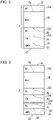
Fig. 2] Fig. 2 is a cross-sectional view of an example of the layers of the lid body shown inFig. 1 . - [
Fig. 3] Fig. 3 is a cross-sectional view of another example of the layers of the lid body shown inFig. 1 . - [
Fig. 4A] Fig. 4A is a photograph of a cross section of a lid body according to the present example. - [
Fig. 4B] Fig. 4B is a photograph of a cross section of a lid body according to a comparative example. - Hereinafter, embodiments of the present disclosure will be described in detail with reference to the drawings. The surface of a lid body facing the inside of a package will be denoted as "lower surface", and the opposite surface, i.e., the surface facing the outside, will be denoted as "upper surface", although these terms do not specify the vertical direction during the use of a lid body, an electronic component accommodation package, and an electronic device. Further, "thickness" denotes the length in a direction perpendicular to the upper surface of the lid body in a cross section perpendicular to the upper surface. The cross section is a cross section of a part excluding the edge of the lid body, where variations in shape are likely to occur. In a case where the lid body includes a structure other than the fourth film on the upper portion thereof, the upper surface denotes the upper surface of the fourth film from which the structure is removed.
- As shown in
Fig. 1 , an electronic component accommodation package 1 according to the present embodiment includes alid body 2 and abase 3 for mounting an electronic component. - The
lid body 2 has a flat plate shape and has anupper surface 21 and alower surface 22. Thelid body 2 includes abase 20, afirst film 22a, and asecond film 22b. Thefirst film 22a is positioned on a lower surface Sb of thebase 20. Further, thesecond film 22b is positioned on a first lower surface S1 of thefirst film 22a. Further, thelid body 2 may include athird film 22c positioned on a second lower surface S2 of thesecond film 22b or abonding material 29 positioned on the second lower surface S2 of thesecond film 22b. Further, in a case where thethird film 22c is positioned on the second lower surface S2 of thesecond film 22a, thebonding material 29 may be positioned on a third lower surface S3 of thethird film 22c. Afourth film 21a may be positioned on an upper surface Sa of thebase 20. - The
base 20 contains an alloy of iron and nickel. Here, the alloy of iron and nickel is, for example, Kovar (Fe-Ni-Co-based alloy). The weight ratio of the components of Kovar is not limited as long as the ratio is in conformity with the international standard ASMT-F15. For example, the weight ratio of the components of Kovar is 53% to 54% iron (Fe), 29% nickel (Ni), and 17% cobalt (Co). Here, Kovar may also contain trace amounts of silicon (Si), manganese (Mn), and the like. In addition, thebase 20 may be formed of Alloy 42 (FE-Ni42). In this case, the weight ratio of Alloy 42 is 42% Ni and 57% Fe, and Alloy 42 contains trace amounts of other metals such as copper (Cu) and manganese (Mn). Further, the ratios of the components described above may have some manufacturing errors. In addition, the thickness of thebase 20 is, for example, in a range of 0.02 to 4 mm. - The
first film 22a is a metal film containing nickel. Further, thefirst film 22a is, for example, formed mainly of nickel and may contain trace amounts of impurities. The thickness of thefirst film 22a is, for example, in a range of 0.002 mm to 0.02 mm. - The
second film 22b is a metal film containing copper (Cu). Further, thesecond film 22b is, for example, formed mainly of copper and may contain trace amounts of impurities. The thickness of thesecond film 22b is, for example, in a range of 0.01 to 1 mm. - The
third film 22c is a metal film containing nickel. Further, thethird film 22c is, for example, formed mainly of nickel and may contain trace amounts of impurities. The thickness of thethird film 22c is, for example, in a range of 0.002 mm to 0.02 mm. - The
fourth film 21a is a metal film containing nickel. Further, thefourth film 21a is, for example, formed mainly of nickel and may contain trace amounts of impurities. The thickness of thefourth film 21a is, for example, in a range of 0.002 mm to 0.02 mm. - The
bonding material 29 is a material for bonding thelid body 2 to thebase 3 for mounting an electronic component described below. Thebonding material 29 contains copper and silver (Ag). Here, thebonding material 29 contains, for example, a silver-copper brazing material. Alternatively, as described below, thebonding material 29 may be a low-melting-point brazing material formed of Au-Sn, a lead-free solder formed of Sn-Ag-Cu, or the like. Further, the thickness of thebonding material 29 is, for example, in a range of 0.05 to 0.5 mm. The bondingmaterial 29 is not limited as long as the material is capable of bonding metal materials to each other. Further, the melting point of thebonding material 29 is approximately 780°C in a case where Ag:Cu = 72:28 and is approximately 850°C in a case where Ag:Cu = 85:15. The melting point can be appropriately selected according to the other configuration and the thickness. In the example shown inFig. 2 or Fig. 3 , thelid body 2 includes aKov base 20 as a base containing Kovar, which is an alloy of iron and nickel, and a Ni film (fourth film) 21a positioned on the upper surface Sa of theKov base 20. - Further, as shown in
Fig. 2 , thelid body 2 includes, as an example of the lower surface laminated structure of theKov base 20, a Ni film (first film) 22a positioned on the lower surface Sb of theKov base 20 and a Cu film (second film) 22b positioned on the lower surface of theNi film 22a. - Further, the
lid body 2 includes aAgCu film 29 as the bonding material positioned on the lower surface of theCu film 22b. - The
base 3 for mounting an electronic component includes abase portion 31 and aframe portion 32. Thebase 3 for mounting an electronic component may be in the form of a one-piece container including thebase portion 31 and theframe portion 32 or in the form of a container in which thebase portion 31 and theframe portion 32 are separate parts. Thebase portion 31 has an upper surface provided with a mounting portion for an electronic component, on which an electronic component 4 is to be mounted. Further, theframe portion 32 is positioned so as to surround the mounting portion, and the lower surface of thelid body 2 is to be bonded to thebase portion 31. In addition, thebase portion 31 has wiring for routing electrodes of the electronic component 4. More specifically, as shown inFig. 1 , the electronic component 4 is mounted on the mounting portion for the electronic component 4 inside thebase 3 for mounting an electronic component. An outer peripheral portion (the surface on which theAgCu film 29 is disposed) of thelower surface 22 of thelid body 2 is bonded to an outerperipheral portion 3a of the upper surface of thebase 3 for mounting an electronic component, and they are welded together using theAgCu film 29 as a brazing material by seam welding, direct seam welding, heating using a baking furnace, or the like. In this manner, theelectronic device 10 is configured such that the electronic component 4 is sealed airtight in the electronic component accommodation package 1. Further, a predetermined metal film is formed on the outerperipheral portion 3a of the upper surface before welding, as necessary (depending on the type of the base material). - The
base 3 for mounting an electronic component is a plate-like member having a rectangular shape when viewed in plan view. Thebase 3 may be formed of an insulating material, for example, a ceramic material such as an aluminum oxide sintered body, a mullite sintered body, a silicon carbide sintered body, an aluminum nitride sintered body, a silicon nitride sintered body, or a glass ceramic. Thebase 3 for mounting an electronic component is not limited to those formed of such ceramic materials. The material of thebase 3 for mounting an electronic component may contain, for example, a resin material, such as an epoxy resin, a polyimide resin, or a polyamide resin, or a composite material obtained by adding glass cloth, an inorganic filler, or the like to such resin materials. The size of thebase 3 for mounting an electronic component is, for example, in a range of 5 mm × 5 mm to 50 mm × 50 mm in plan view and the thickness thereof is in a range of 0.3 mm to 3 mm. Further, in a case where thebase 3 for mounting an electronic component contains a metal material, a structure from which heat generated by the electronic component 4 is efficiently released to the outside of the package 1 can be obtained. - The inner edge and the outer edge of the
frame portion 32 each have a rectangular frame shape in plan view. Each side of theframe portion 32 in the rectangular frame shape is provided parallel to the corresponding side of thebase 3 for mounting an electronic component. Further, theframe portion 32 may have a metal layer on the upper surface thereof, which is the surface facing thelid body 2. Further, in a case where theframe portion 32 is provided integrally with the upper surface of thebase 3 for mounting an electronic component, theframe portion 32 formed of a ceramic material may be provided by being baked simultaneously with thebase 3 for mounting an electronic component. Further, in a case where theframe portion 32 and thebase portion 31 are separately provided, the metal layer positioned on the upper surface of thebase 3 for mounting an electronic component and the metal layer positioned on the lower surface of theframe portion 32 may be bonded to each other with a bonding material such as a low-melting-point brazing material formed of gold (Au)-tin (Sn) . - In addition, a metal material such as iron, copper, nickel, chromium, cobalt, or tungsten or an alloy formed of such metals can be used as the
frame portion 32. The size of theframe portion 32 is, for example, in a range of 5 mm × 5 mm to 50 mm × 50 mm and the thickness thereof is in a range of 0.5 mm to 2 mm in plan view. Further, the height of theframe portion 32 is, for example, in a range of 1 mm to 10 mm. - The
lid body 2 is bonded to the upper surface of theframe portion 32 by using a bonding material such as a brazing material or solder such that the inside of theframe portion 32 is blocked. Thelid body 2 has a rectangular shape in plan view, and has a bonding region to be bonded to the upper surface of theframe portion 32 that is the surface facing thelid body 2 is provided on the lower surface of thelid body 2 that is the surface facing theframe portion 32. - With the above-described configuration, the electronic component accommodation package 1 according to the embodiment of the present invention described above is capable of satisfactorily maintaining the package in a sealed state.
- The
electronic device 10 according to the embodiment of the present disclosure is completed by installing the electronic component 4 in an installation region of the electronic component accommodation package 1 described above and electrically connecting the electronic component 4 to a first electrode portion of the electronic component accommodation package 1. The electronic component 4 is installed on the metal portion provided in the installation region by using a bonding material such as a low-melting-point brazing material formed of Au-Sn or a lead-free solder formed of Sn-silver (Ag)-copper (Cu). Examples of the electronic component 4 include ICs, LSIs, and semiconductor elements for power devices. - Further, the electronic component 4 is sealed in the
electronic device 10 by bonding and fixing thelid body 2 to the upper surface of theframe portion 32 as a lid in a state where the electronic component 4 is mounted (installed) on the mounting portion. Here, the upper surface of theframe portion 32 and the bonding region of thelid body 2 are bonded to each other with an adhesive or an adhesive containing thebonding material 29. The adhesive is, for example, silver-copper, as described above, or another material such as a low-melting-point brazing material formed of Au-Sn or a lead-free solder formed of Sn-Ag-Cu. - In a case where the
frame portion 32 of the electronic component accommodation package 1 and thelid body 2 are bonded to each other with thebonding material 29, the bonding is carried out by a seam welding method or the like. In this case, heat is locally applied to thelid body 2, which tends to cause thermal expansion and thermal contraction. As shown inFig. 2 , an alloy film is formed between thesecond film 22b and thebonding material 29 in a case where thebonding material 29 is bonded to thesecond film 22b of thelid body 2. The alloy film is formed of an alloy of copper and silver. Here, penetration of the crystal grain boundaries of the base 20 by Cu of thesecond film 22b and AgCu of thebonding material 29 is reduced because thefirst film 22a is positioned between the base 20 and thesecond film 22b. Further, in a case where thethird film 22c is provided in thelid body 2 as shown inFig. 3 , afirst alloy film 22d is generated between thesecond film 22b and thethird film 22c due to the heat during welding. In this manner, the possibility of the material of thesecond film 22b coupling with the material of thebonding material 29 due to the heat during bonding can be reduced. Therefore, the possibility of variations in the melting point of thebonding material 29 can be reduced, and unevenness in bonding during welding due to variations in the melting point of thebonding material 29 can also be reduced. Further, in a case where thebonding material 29 contains silver and copper and thethird film 22c is formed of a metal, such as nickel, asecond alloy film 22e containing silver, copper, and nickel is easily generated. Accordingly, the possibility of the material of thesecond film 22b coupling with the material of thebonding material 29 due to the heat during bonding can be reduced as described above. Thefirst alloy film 22d may be positioned partially or entirely between thesecond film 22b and thethird film 22c. In a case where thefirst alloy film 22d is positioned entirely between thesecond film 22b and thethird film 22c, the possibility of the material of thesecond film 22b coupling with the material of thebonding material 29 due to the heat during bonding can be further reduced. Thesecond alloy film 22e may be positioned partially or entirely between thethird film 22c and thebonding material 29. In a case where thesecond alloy film 22e is positioned entirely between thethird film 22c and thebonding material 29, the possibility of the material of thesecond film 22b coupling with the material of thebonding material 29 due to the heat during bonding can be further reduced. - Further, the first film (22a) and the fourth film (21a) may be formed of identical materials. In this case, since the upper and lower layers of the base 20 can be sandwiched between the materials with an identical thermal expansion coefficient, deformation and warpage of the
base 20 due to the heat and the like generated during welding of thelid body 2 can be reduced. Here, "identical materials" includes materials containing different impurities and materials containing different amounts of impurities within a range where the impurities do not affect thermal expansion. Further, in a case where the thickness of thefirst film 22a is identical to the thickness of thefourth film 21a, since the upper and lower layers of the base 20 can be sandwiched with similar thermal expansion, deformation and warpage of thebase 20 due to the heat and the like generated during welding of thelid body 2 can be further reduced. Here, "identical" may include errors during measurement of the thickness, manufacturing errors, and the like. For example, in a case where the thickness of thefourth film 21a is within ±10% of the thickness of thefirst film 22a, the thickness of thefourth film 21a can be considered to be identical to the thickness of thefirst film 22a. - Further, the thickness of the
second film 22b may be greater than each of the thickness of thefirst film 22a, the thickness of thethird film 22c, and the thickness of thefourth film 21a. Thesecond film 22b contains copper and thus has a lower elastic modulus than in other configurations. Therefore, the amount of deformation of thelid body 2 due to the thermal stress can be further reduced by increasing the thickness of thesecond film 22b in a case of applying heat during bonding of thelid body 2 to thebase 3 for mounting an electronic component. Accordingly, in a case of carrying out welding or the like, thelid body 2 can be bonded to thebase 3 for mounting an electronic component with a lower pressure. As a result, the load applied to thebase 3 for mounting an electronic component can be reduced. In this manner, the possibility of mechanical loss, such as cracks, occurring in thelid body 2 and thebase 3 for mounting an electronic component can be reduced. - Further, the
third film 22c and thefirst film 22a may be formed of identical materials. In this case, since the upper and lower layers of thesecond film 22b can be sandwiched between the materials with an identical thermal expansion coefficient, deformation and warpage of thesecond film 22b due to the heat and the like generated during welding of thelid body 2 can be reduced. Here, "identical materials" includes materials containing different impurities and materials containing different amounts of impurities within a range where the impurities do not affect thermal expansion. Further, in a case where the thickness of thefirst film 22a is identical to the thickness of thethird film 22c, since the upper and lower layers of thesecond film 22b can be sandwiched with similar thermal expansion, deformation and warpage of thesecond film 22b due to the heat and the like generated during welding of thelid body 2 can be further reduced. Here, "identical" may include errors during the measurement of the thickness, manufacturing errors, and the like. For example, in a case where the thickness of thethird film 22c is within ±10% of the thickness of thefirst film 22a, the thickness of thethird film 22c can be considered to be identical to the thickness of thefirst film 22a. - Further, as described above, the
first alloy film 22d is formed between thethird film 22c and thesecond film 22b with the heat generated during bonding of thelid body 2 to thebase 3 for mounting an electronic component. Therefore, the thickness of thethird film 22c of thelid body 2 bonded to thebase 3 for mounting an electronic component may be less than the thickness of thefirst film 22a. - Hereinafter, a method of producing the electronic component accommodation package 1 according to the embodiment of the present disclosure will be described.
- In a case where the
base portion 31 of thebase 3 for mounting an electronic component is formed of an aluminum oxide sintered body, thebase portion 31 is prepared in the following manner. First, ceramic green sheets are prepared in a rectangular sheet shape by forming a raw material powder, such as aluminum oxide or silicon oxide, into a sheet shape together with an appropriate organic binder and an appropriate organic solvent. Next, a laminate composed of the ceramic green sheets is prepared by laminating a plurality of ceramic green sheets. Further, a plurality of ceramic green sheets are not necessarily laminated to obtain a laminate, and the laminate may be formed of only one layer as long as there is no problem in terms of mechanical strength and the like as thebase portion 31 of thebase 3 for mounting an electronic component. Thereafter, these ceramic green sheets are baked at a temperature of 1300°C to 1600°C, thereby preparing thebase portion 31 of thebase 3 for mounting an electronic component. - In a case where the
frame portion 32 is formed of, for example, an aluminum oxide sintered body, theframe portion 32 is prepared in the same manner as for thebase 3 for mounting an electronic component described above. First, ceramic green sheets are prepared in a rectangular sheet shape by forming a raw material powder, such as aluminum oxide or silicon oxide, into a sheet shape together with an appropriate organic binder and an appropriate organic solvent. Next, a laminate composed of the ceramic green sheet is prepared by laminating a plurality of ceramic green sheets. Further, the laminate is formed into a frame shape by providing a through-hole in the central portion according to a punch working method. In addition, a metal layer is provided on the upper surface of the laminate by printing a metal paste prepared by mixing a powder of tungsten, an organic solvent, and an organic binder by using a method, such as a screen printing method. Thereafter, theframe portion 32 is obtained by baking the laminate at a temperature of 1300°C to 1600°C. Further, theframe portion 32 is not necessarily formed by laminating a plurality of ceramic green sheets and may be formed of only one layer as long as there is no problem in terms of mechanical strength and the like as theframe portion 32. Further, theframe portion 32 is bonded to the upper surface of thebase 3 for mounting an electronic component with a bonding material such as a glass bonding material or a resin bonding material. In a case where theframe portion 32 is formed of an aluminum oxide sintered body similar to that of thebase 3 for mounting an electronic component, theframe portion 32 is formed integrally with thebase portion 31 by a method of laminating frame-like ceramic green sheets on the upper surface of ceramic green sheets for forming thebase 3 for mounting an electronic component and simultaneously baking these ceramic green sheets. - The
lid body 2 is formed by stacking together the base and the respective films, performing pressure bonding with a pressure bonding machine to form a clad material, and processing the clad material to a predetermined size. In this case, the thickness of each configuration to be prepared is determined in advance in consideration of the compression ratio of each material so that thelid body 2 has a predetermined thickness. Alternatively, an iron-nickel-cobalt alloy and nickel, and nickel and copper, are pressure-bonded to form a clad material, the clad material is processed to a predetermined size, and the upper surface and the lower surface of the clad material are subjected to nickel plating. - The penetration of the crystal grain boundaries of the
Kov base 20 by Cu of theCu film 22b and AgCu of theAgCu film 29 during welding of thelid body 2 and thebase 3 for mounting an electronic component is reduced by theNi film 22a. Therefore, occurrence of cracks in theKov base 20 is reduced, and thus a package with high airtightness can be formed. - The
lid body 2 may include, as another example of the lower surface laminated structure of theKov base 20, as shown inFig. 3 , theNi film 22a positioned on the lower surface Sb of theKov base 20, theCu film 22b positioned on the lower surface of theNi film 22a, and the Ni film (third film) 22c positioned on the lower surface of theCu film 22b. - Further, the
lid body 2 may include theAgCu film 29 as the bonding material positioned on the lower surface of theNi film 22c. - In a case of such a laminated structure, the penetration of the
Kov base 20 by Cu and AgCu as described above can be reduced, and the possibility of Cu of theCu film 22b coupling with Cu of theAgCu film 29 due to heat during welding can be reduced because theNi film 22c is interposed between theCu film 22b and theAgCu film 29. In this manner, the possibility of a change in the melting point of theAgCu film 29, which functions as a coupling material, due to theCu film 22b coupling with theAgCu film 29 when heat is applied can be reduced, compared with a case where theNi film 22c is not provided. - Therefore, the bonding reliability of the
lid body 2 is stabilized by stabilizing the melting point of the bonding material (29) and occurrence of cracks in theKov base 20 is reduced, and thus a package with high airtightness can be formed. - The
AgCu film 29 shown inFigs. 2 and 3 bonds thelid body 2 to thebase 3 for mounting an electronic component in theelectronic device 10. TheAgCu film 29 may be positioned as a part of thelid body 2 or may be positioned on the outerperipheral portion 3a of the upper surface of thebase 3 for mounting an electronic component. Further, theAgCu film 29 may be separately positioned between thebase 3 for mounting an electronic component and thelid body 2. By disposing theAgCu film 29 on thelid body 2 in advance, the labor of separately preparing the bonding material can be reduced in a case where thelid body 2 is bonded as a lid body for a semiconductor device package or the like, and thus productivity can be improved. The bonding material may be a low-melting-point brazing material formed of Au-Sn, a lead-free solder formed of Sn-Ag-Cu, or the like, in place of theAgCu film 29. -
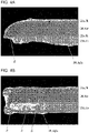
Fig. 4A is a photograph of a cross section of a lid body of the present example according to the embodiment shown inFig. 2 .Fig. 4B is a photograph of a cross section of a lid body of a comparative example. Both lid bodies of the present example and the comparative example were obtained by being baked in a baking furnace at 850°C for approximately 3.6 minutes. - In the present example shown in
Fig. 4A , theNi film 22a is interposed between theKov base 20 and theCu film 22b. - Meanwhile, in the comparative example shown in
Fig. 4B , theCu film 22b is in contact with theKov base 20. Further, in the comparative example shown inFig. 4B , the laminated elements corresponding to those of the example according to the present invention are denoted by the same reference numerals. - In the comparative example, Cu of the
Cu film 22b and AgCu of theAgCu film 29 penetrate the crystal grain boundaries of theKov base 20. Eroded parts E were confirmed inFig. 4B . The formation of the eroded parts E is the cause of occurrence of cracks in theKov base 20. - In contrast, in the example of the present invention, penetration of the crystal grain boundaries of the
Kov base 20 by Cu of theCu film 22b and AgCu of theAgCu film 29 is reduced by theNi film 22a. As shown inFig. 4A , a significant decrease in the amount of the eroded parts E in theKov base 20 compared with the comparative example was confirmed. In this manner, occurrence of cracks in theKov base 20 is reduced, and thus a package with high airtightness can be formed. - Further, the
lid body 2 may be positioned at least in the bonding region that is bonded to the electronic component accommodation package 1. Here, thelid body 2 may have a flat plate shape or a shape in which thelid body 2 has a recess in the central portion. In this manner, thermal deformation, a change in the melting point of the bonding material, and the like during bonding of thelid body 2 to the electronic component accommodation package 1 can be efficiently reduced. - The embodiments of the present disclosure have been described above. However, the present disclosure is not limited to the above-described embodiments. For example, the details shown in the embodiments and the drawings, such as the materials, the shapes, the sizes, and the like of the respective portions of the lid body and the base for mounting an electronic component, can be appropriately changed without departing from the scope of the disclosure.
- The present disclosure can be applied to lid bodies, electronic component accommodation packages, and electronic devices.
-
- 1
- electronic component accommodation package
- 2
- lid body
- 3
- base for mounting electronic component
- 3a
- outer peripheral portion of upper surface
- 4
- electronic component
- 10
- electronic device
- 20
- Kov base (base)
- 21a
- Ni film (fourth film)
- 22a
- Ni film (first film)
- 22b
- Cu film (second film)
- 22c
- Ni film (third film)
- 29
- AgCu film (bonding material)
- Sa
- upper surface of Kov base
- Sb
- lower surface of Kov base
- S1
- first lower surface
- S2
- second lower surface
- S3
- third lower surface
Claims (13)
- A lid body comprising:a base which contains an alloy of iron and nickel;a first film which is positioned on a lower surface of the base and which contains nickel; anda second film which is positioned on a first lower surface of the first film and which contains copper.
- The lid body according to claim 1, further comprising a bonding material which is positioned on a second lower surface of the second film.
- The lid body according to claim 1, further comprising a third film which is positioned on a second lower surface of the second film and which contains nickel.
- The lid body according to claim 3, further comprising a bonding material which is positioned on a third lower surface of the third film.
- The lid body according to claim 2 or 4, wherein the bonding material contains copper and silver.
- The lid body according to any one of claims 1 to 5, further comprising a fourth film which is positioned on an upper surface of the base and which contains nickel.
- The lid body according to claim 6, wherein the first film and the fourth film are formed of an identical material.
- The lid body according to claim 3 or 4, wherein a first alloy film containing copper and nickel is positioned between the second film and the third film.
- The lid body according to any one of claims 1 to 8, wherein the second film has a thickness greater than a thickness of the first film.
- The lid body according to claim 6 or 7, wherein the first film has a thickness identical to a thickness of the fourth film.
- The lid body according to claim 3, 4, or 8, wherein the first film and the third film are formed of an identical material.
- An electronic component accommodation package comprising:the lid body according to any one of claims 1 to 11; anda base for mounting an electronic component, including a base portion having an upper surface provided with a mounting portion on which an electronic component is to be mounted, and a frame portion which is positioned on the upper surface of the base portion, which surrounds the mounting portion, and to which a lower surface of the lid body is to be bonded.
- An electronic device comprising the electronic component accommodation package according to claim 12 and an electronic component mounted on the mounting portion.
Applications Claiming Priority (2)
| Application Number | Priority Date | Filing Date | Title |
|---|---|---|---|
| JP2019178705 | 2019-09-30 | ||
| PCT/JP2020/037188 WO2021066024A1 (en) | 2019-09-30 | 2020-09-30 | Lid body, electronic component accommodation package, and electronic device |
Publications (2)
| Publication Number | Publication Date |
|---|---|
| EP4040475A1 true EP4040475A1 (en) | 2022-08-10 |
| EP4040475A4 EP4040475A4 (en) | 2023-11-08 |
Family
ID=75338406
Family Applications (1)
| Application Number | Title | Priority Date | Filing Date |
|---|---|---|---|
| EP20870626.7A Withdrawn EP4040475A4 (en) | 2019-09-30 | 2020-09-30 | COVER BODY, ELECTRONIC COMPONENT HOUSING AND ELECTRONIC DEVICE |
Country Status (5)
| Country | Link |
|---|---|
| US (1) | US12394679B2 (en) |
| EP (1) | EP4040475A4 (en) |
| JP (1) | JP7379515B2 (en) |
| CN (1) | CN114430859A (en) |
| WO (1) | WO2021066024A1 (en) |
Families Citing this family (2)
| Publication number | Priority date | Publication date | Assignee | Title |
|---|---|---|---|---|
| JPWO2022239620A1 (en) * | 2021-05-13 | 2022-11-17 | ||
| WO2025047374A1 (en) * | 2023-08-25 | 2025-03-06 | 京セラ株式会社 | Lid body, package for mounting optical component therein, optical device, and optical module |
Family Cites Families (21)
| Publication number | Priority date | Publication date | Assignee | Title |
|---|---|---|---|---|
| KR100856610B1 (en) | 2001-03-27 | 2008-09-03 | 가부시키가이샤 네오맥스 마테리아르 | Package for electronic parts and manufacturing method |
| JP3850787B2 (en) | 2001-11-12 | 2006-11-29 | 株式会社Neomaxマテリアル | Electronic component package, its lid, lid for the lid, and method for manufacturing the lid |
| JP2003158211A (en) * | 2001-11-19 | 2003-05-30 | Daishinku Corp | Package for electronic component and piezoelectric vibration device using the same |
| US6627814B1 (en) * | 2002-03-22 | 2003-09-30 | David H. Stark | Hermetically sealed micro-device package with window |
| JP4071191B2 (en) | 2003-12-22 | 2008-04-02 | 田中貴金属工業株式会社 | Electronic component package lid |
| WO2007094284A1 (en) * | 2006-02-15 | 2007-08-23 | Neomax Materials Co., Ltd. | Cap for airtight sealing, package for housing electronic part, and process for producing airtightly sealing cap |
| JP5312274B2 (en) * | 2009-09-28 | 2013-10-09 | 京セラ株式会社 | Electronic component storage package and electronic device |
| JPWO2013061511A1 (en) * | 2011-10-27 | 2015-04-02 | パナソニック株式会社 | Light emitting device |
| JP5885690B2 (en) * | 2012-04-27 | 2016-03-15 | キヤノン株式会社 | Electronic components and equipment |
| WO2014073665A1 (en) * | 2012-11-12 | 2014-05-15 | 株式会社Neomaxマテリアル | Cover material for hermitic sealing and package for containing electronic component |
| JP2014197575A (en) * | 2013-03-29 | 2014-10-16 | セイコーエプソン株式会社 | Package, electronic device, method of manufacturing electronic device, electronic apparatus, and mobile body |
| JP6314406B2 (en) * | 2013-10-03 | 2018-04-25 | 日立金属株式会社 | HERMETIC SEALING CAP, ELECTRONIC COMPONENT STORAGE PACKAGE, AND HERMETIC SEALING CAP MANUFACTURING METHOD |
| JP2016006820A (en) * | 2014-06-20 | 2016-01-14 | 大和電機工業株式会社 | Sealing member and method for manufacturing electronic component package |
| JP6387818B2 (en) * | 2014-12-11 | 2018-09-12 | 日立金属株式会社 | Method of manufacturing hermetic sealing lid |
| JP6421595B2 (en) * | 2014-12-26 | 2018-11-14 | 日立金属株式会社 | Hermetic sealing lid material, method for manufacturing hermetic sealing lid material, and electronic component storage package |
| JP2016139758A (en) * | 2015-01-29 | 2016-08-04 | 株式会社日立金属ネオマテリアル | Airtight sealing lid and electronic component housing package |
| US10396002B2 (en) * | 2015-03-24 | 2019-08-27 | Kyocera Corporation | Electronic component storage substrate and housing package |
| JP2017011237A (en) * | 2015-06-26 | 2017-01-12 | セイコーエプソン株式会社 | Lid, package, electronic device, electronic device, and moving body |
| JP6787662B2 (en) * | 2015-12-22 | 2020-11-18 | 京セラ株式会社 | Seal ring, electronic component storage package, electronic device and manufacturing method of these |
| JP7083898B2 (en) * | 2018-06-28 | 2022-06-13 | 京セラ株式会社 | Hypokeimenon and semiconductor devices |
| CN116097501A (en) * | 2020-08-07 | 2023-05-09 | 京瓷株式会社 | Battery package and battery module |
-
2020
- 2020-09-30 US US17/763,352 patent/US12394679B2/en active Active
- 2020-09-30 WO PCT/JP2020/037188 patent/WO2021066024A1/en not_active Ceased
- 2020-09-30 JP JP2021551384A patent/JP7379515B2/en active Active
- 2020-09-30 CN CN202080066700.4A patent/CN114430859A/en active Pending
- 2020-09-30 EP EP20870626.7A patent/EP4040475A4/en not_active Withdrawn
Also Published As
| Publication number | Publication date |
|---|---|
| US12394679B2 (en) | 2025-08-19 |
| WO2021066024A1 (en) | 2021-04-08 |
| JP7379515B2 (en) | 2023-11-14 |
| CN114430859A (en) | 2022-05-03 |
| JPWO2021066024A1 (en) | 2021-04-08 |
| EP4040475A4 (en) | 2023-11-08 |
| US20220344226A1 (en) | 2022-10-27 |
Similar Documents
| Publication | Publication Date | Title |
|---|---|---|
| JP6791719B2 (en) | Substrate for mounting electronic components, electronic devices and electronic modules | |
| US12394679B2 (en) | Lid body, electronic component accommodation package, and electronic device | |
| KR20200135378A (en) | Electronic component mounting module | |
| JP5388601B2 (en) | Electronic component storage package | |
| CN112352309B (en) | Substrate and semiconductor device | |
| JP6408423B2 (en) | Package and electronic equipment | |
| JP2005072421A (en) | Electronic component storage package and electronic device | |
| JP4511376B2 (en) | Connection terminal and electronic component storage package and electronic device using the same | |
| US11437296B2 (en) | Semiconductor package, semiconductor apparatus, and method for manufacturing semiconductor package | |
| US20210066159A1 (en) | Heat dissipation board and electronic apparatus | |
| JP3935054B2 (en) | Wiring board | |
| JP6698492B2 (en) | Semiconductor package and semiconductor device | |
| JP2019076939A (en) | Brazing material, junction structure, and semiconductor package | |
| JP5409066B2 (en) | Electronic component storage package | |
| JP3898567B2 (en) | Electronic component storage package | |
| JP4105968B2 (en) | Electronic component mounting substrate and electronic device using the same | |
| JP2017174872A (en) | Semiconductor element storage package and semiconductor device | |
| JP2003258138A (en) | Semiconductor device | |
| JP3872399B2 (en) | Wiring board | |
| JP2003338571A (en) | Electronic component mounting board and electronic device using the same | |
| JP2004022841A (en) | Wiring board | |
| JP2003303910A (en) | Wiring board | |
| JP2002164456A (en) | Electronic component storage package | |
| JP2012134301A (en) | Wiring board | |
| JP2002164457A (en) | Electronic component storage package |
Legal Events
| Date | Code | Title | Description |
|---|---|---|---|
| STAA | Information on the status of an ep patent application or granted ep patent |
Free format text: STATUS: THE INTERNATIONAL PUBLICATION HAS BEEN MADE |
|
| PUAI | Public reference made under article 153(3) epc to a published international application that has entered the european phase |
Free format text: ORIGINAL CODE: 0009012 |
|
| STAA | Information on the status of an ep patent application or granted ep patent |
Free format text: STATUS: REQUEST FOR EXAMINATION WAS MADE |
|
| 17P | Request for examination filed |
Effective date: 20220323 |
|
| AK | Designated contracting states |
Kind code of ref document: A1 Designated state(s): AL AT BE BG CH CY CZ DE DK EE ES FI FR GB GR HR HU IE IS IT LI LT LU LV MC MK MT NL NO PL PT RO RS SE SI SK SM TR |
|
| DAV | Request for validation of the european patent (deleted) | ||
| DAX | Request for extension of the european patent (deleted) | ||
| P01 | Opt-out of the competence of the unified patent court (upc) registered |
Effective date: 20230505 |
|
| REG | Reference to a national code |
Ref country code: DE Ref legal event code: R079 Free format text: PREVIOUS MAIN CLASS: H01L0023020000 Ipc: H01L0023040000 |
|
| A4 | Supplementary search report drawn up and despatched |
Effective date: 20231006 |
|
| RIC1 | Information provided on ipc code assigned before grant |
Ipc: H01L 23/00 20060101ALI20230929BHEP Ipc: H01L 23/10 20060101ALI20230929BHEP Ipc: H01L 23/06 20060101ALI20230929BHEP Ipc: H01L 23/04 20060101AFI20230929BHEP |
|
| STAA | Information on the status of an ep patent application or granted ep patent |
Free format text: STATUS: THE APPLICATION HAS BEEN WITHDRAWN |
|
| 18W | Application withdrawn |
Effective date: 20251002 |