EP4033609B1 - Antennenanordnung und und drahtlose vorrichtung - Google Patents
Antennenanordnung und und drahtlose vorrichtung Download PDFInfo
- Publication number
- EP4033609B1 EP4033609B1 EP20878136.9A EP20878136A EP4033609B1 EP 4033609 B1 EP4033609 B1 EP 4033609B1 EP 20878136 A EP20878136 A EP 20878136A EP 4033609 B1 EP4033609 B1 EP 4033609B1
- Authority
- EP
- European Patent Office
- Prior art keywords
- antenna assembly
- elements
- network
- pcb
- lines
- Prior art date
- Legal status (The legal status is an assumption and is not a legal conclusion. Google has not performed a legal analysis and makes no representation as to the accuracy of the status listed.)
- Active
Links
Images


Classifications
-
- H—ELECTRICITY
- H01—ELECTRIC ELEMENTS
- H01Q—ANTENNAS, i.e. RADIO AERIALS
- H01Q1/00—Details of, or arrangements associated with, antennas
- H01Q1/12—Supports; Mounting means
- H01Q1/22—Supports; Mounting means by structural association with other equipment or articles
- H01Q1/2291—Supports; Mounting means by structural association with other equipment or articles used in Bluetooth® or Wi-Fi® devices of Wireless Local Area Networks [WLAN]
-
- H—ELECTRICITY
- H01—ELECTRIC ELEMENTS
- H01Q—ANTENNAS, i.e. RADIO AERIALS
- H01Q1/00—Details of, or arrangements associated with, antennas
- H01Q1/52—Means for reducing coupling between antennas; Means for reducing coupling between an antenna and another structure
-
- H—ELECTRICITY
- H01—ELECTRIC ELEMENTS
- H01Q—ANTENNAS, i.e. RADIO AERIALS
- H01Q21/00—Antenna arrays or systems
- H01Q21/0006—Particular feeding systems
-
- H—ELECTRICITY
- H01—ELECTRIC ELEMENTS
- H01Q—ANTENNAS, i.e. RADIO AERIALS
- H01Q21/00—Antenna arrays or systems
- H01Q21/0006—Particular feeding systems
- H01Q21/0075—Stripline fed arrays
-
- H—ELECTRICITY
- H01—ELECTRIC ELEMENTS
- H01Q—ANTENNAS, i.e. RADIO AERIALS
- H01Q21/00—Antenna arrays or systems
- H01Q21/06—Arrays of individually energised antenna units similarly polarised and spaced apart
- H01Q21/20—Arrays of individually energised antenna units similarly polarised and spaced apart the units being spaced along or adjacent to a curvilinear path
- H01Q21/205—Arrays of individually energised antenna units similarly polarised and spaced apart the units being spaced along or adjacent to a curvilinear path providing an omnidirectional coverage
-
- H—ELECTRICITY
- H01—ELECTRIC ELEMENTS
- H01Q—ANTENNAS, i.e. RADIO AERIALS
- H01Q23/00—Antennas with active circuits or circuit elements integrated within them or attached to them
-
- H—ELECTRICITY
- H01—ELECTRIC ELEMENTS
- H01Q—ANTENNAS, i.e. RADIO AERIALS
- H01Q9/00—Electrically-short antennas having dimensions not more than twice the operating wavelength and consisting of conductive active radiating elements
- H01Q9/04—Resonant antennas
- H01Q9/06—Details
- H01Q9/065—Microstrip dipole antennas
-
- H—ELECTRICITY
- H01—ELECTRIC ELEMENTS
- H01Q—ANTENNAS, i.e. RADIO AERIALS
- H01Q9/00—Electrically-short antennas having dimensions not more than twice the operating wavelength and consisting of conductive active radiating elements
- H01Q9/04—Resonant antennas
- H01Q9/16—Resonant antennas with feed intermediate between the extremities of the antenna, e.g. centre-fed dipole
Definitions
- This application relates to the field of communication technologies, and in particular, to an antenna assembly and a wireless device.
- a wireless access point may provide large signal coverage by using an omnidirectional antenna, to meet a communication capacity requirement.
- AP access point
- An interference suppression capability of an entire network depends on a side lobe suppression capability of the omnidirectional antenna.
- the omnidirectional antenna mainly includes a dipole antenna, a monopole antenna, a slot antenna, and the like.
- the dipole antenna usually approximates a point source, and has a wide beamwidth and a weak side lobe suppression capability.
- CN 107240783 A discloses a dual-mode reuse vortex electromagnetic wave antenna.
- CN 104157980 A discloses a reconfigurable micro-strip yagi antenna.
- US 2012/276854 A1 discloses a slot antenna for an implantable device.
- US 4672386 A discloses an antenna with radial and edge solt radiators fed with stripline.
- US 2005/099356 A1 discloses a multiband radially distributed graded phased array antenna.
- US 2003/218571 A1 discloses a planar antenna having linear and circular polarization.
- CN 106410397 A discloses a printed dipole oscillator.
- This application provides an antenna assembly and a wireless device, to resolve a problem that an omnidirectional antenna has a week side lobe suppression capability.
- Technical solutions are as follows.
- an antenna assembly includes N elements, a feeding network, and a printed circuit board (printed circuit board, PCB).
- N is an integer greater than or equal to 3.
- the N elements and the feeding network are located on the PCB.
- the N elements are all connected to the feeding network.
- Each element has a radial part. The radial part of each element points to an antenna phase center, and a length of the radial part of each element is greater than a sum of lengths of other non-radial parts.
- each element 301 is equivalent to a line source, and has a relatively narrow beamwidth and an enhanced side lobe suppression capability.
- N is an even number, there are a plurality of element pairs in the N elements, and the elements in each element pair are centrosymmetrical with each other with respect to the antenna phase center.
- a distance between the two elements in each element pair is a preset multiple of an operating wavelength of the antenna assembly.
- the present multiple is any value from 0.25 to 1.
- N dipole elements may be divided into a plurality of dipole element pairs, and the two elements in each element pair are centrosymmetrical with each other with respect to the antenna phase center.
- a distance between two elements may be set based on a use scenario, so that radiation intensity of the antenna assembly at different radiation angles is adjusted, to further adjust a side lobe suppression capability of the antenna assembly.
- the feeding network is a double-sided parallel strip line (double-sided parallel strip line, DSPSL) power division network.
- the N elements are N dipole elements.
- Each dipole element includes two arms. One of the two arms is located on an upper surface of the PCB and is connected to one end of an arc-shaped strip line that is located on the upper surface of the PCB and that is in the double-sided parallel strip line power division network.
- the other arm is located on a lower surface of the PCB and is connected to one end of an arc-shaped strip line that is located on the lower surface of the PCB and that is in the double-sided parallel strip line power division network.
- the arc-shaped strip lines connected to the two arms are mirror-symmetrical with each other with respect to the PCB, and connection points between the two arms and the arc-shaped strip lines are mirror-symmetrical with each other with respect to the PCB.
- the double-sided parallel strip line power division network includes an upper surface network and a lower surface network.
- the upper surface network is located on the upper surface of the PCB, and the lower surface network is located on the lower surface of the PCB.
- the upper surface network and the lower surface network are mirror-symmetrical with each other with respect to the PCB.
- the upper surface network and the lower surface network each include a first power splitter, a plurality of linear strip lines, a plurality of impedance transformation lines, a second power splitter, and a plurality of arc-shaped strip lines.
- the first power splitter is configured to connect the plurality of linear strip lines and the plurality of arc-shaped strip lines.
- Each of the plurality of linear strip lines is connected to one of the plurality of impedance transformation lines.
- the second power splitter is configured to connect the plurality of impedance transformation lines.
- a length of each of the two arms is a specified multiple of an operating wavelength of the antenna assembly.
- the specified multiple is any value from 0.125 to 1.
- a first arm in the two arms includes a non-radial part, the first arm is L-shaped, a second arm does not include a non-radial part, and a distance between the first arm and the antenna phase center is greater than a distance between the second arm and the antenna phase center.
- one arm, away from the antenna phase center, in the two arms of each dipole element may be L-shaped, and the other arm may not include a non-radial part. In this way, an area occupied by the feeding network and the dipole element may be reduced, so that an antenna size is reduced.
- a distance between a first dipole element and a second dipole element that are centrosymmetrical with each other in the N dipole elements refers to a distance between a first connection point and a second connection point
- the first connection point is a connection point between the first dipole element and the arc-shaped strip line
- the second connection point is a connection point between the second dipole element and the arc-shaped strip line.
- a wireless device includes a baseband circuit, a radio frequency circuit, and the antenna assembly described in the first aspect.
- the radio frequency circuit is configured to work with the antenna assembly to implement transmission and reception of a radio signal, and the baseband circuit is configured to process the radio signal.
- FIG. 1 is a diagram of an application scenario of an antenna assembly according to an embodiment of this application. As shown in FIG. 1 , the scenario includes a controller 101, an access point (access point, AP) 102, and a plurality of terminals 103.
- AP access point
- the controller 101 may be configured to manage and configure a plurality of APs 102 in a centralized manner, and forward user data.
- An AP is used to provide a wireless access service for the plurality of terminals 103 that are connected.
- the AP is usually disposed at a height of 3 to 5 m (m), and has a cell covering radius reaching 5 to 8 m.
- a quantity of users per unit area is usually large. Therefore, a large-angle omnidirectional antenna may be used in the AP for signal coverage, to ensure communication capacity.
- a distance between APs operating at a same frequency is usually small. In this case, there is signal interference between the APs operating at the same frequency.
- this embodiment of this application provides an antenna assembly used in an AP, to improve an interference suppression capability of the AP. Therefore, signal interference between APs operating at a same frequency is reduced.
- the AP 102 may be a network device, for example, a base station, a router, or a switch, and the plurality of terminals 103 may be mobile phones, computers, or the like.
- the plurality of terminals 103 may be mobile phones, computers, or the like.
- FIG. 1 only three terminals are used as an example for description, and this does not constitute a limitation on a quantity of terminals in the application scenario provided in this embodiment of this application.
- FIG. 2 is a schematic diagram of a structure of a network device according to an embodiment of this application.
- the AP in FIG. 1 may be implemented by a network device shown in FIG. 2 .
- the network device includes a processor 201, a communication bus 202, a memory 203, a radio frequency circuit 204, an antenna assembly 205, and a baseband circuit 206.
- the processor 201 may be a common central processing unit (central processing unit, CPU), a microprocessor, an application-specific integrated circuit (application-specific integrated circuit, ASIC), or one or more integrated circuits.
- CPU central processing unit
- ASIC application-specific integrated circuit
- the communication bus 202 may include a channel for transmitting information between the foregoing components.
- the memory 203 may be a read-only memory (read-only memory, ROM), another type of static storage device that can store static information and instructions, a random access memory (random access memory, RAM), another type of dynamic storage device that can store information and instructions, an electrically erasable programmable read-only memory (EEPROM), an optical disc, a magnetic disk, another magnetic storage device, or any other media capable of carrying or storing desired program code in the form of an instruction or a data structure and capable of being accessed by a computer.
- the memory 203 may exist independently and is connected to the processor 201.
- the memory 203 may alternatively be integrated with the processor 201.
- the radio frequency circuit 204 works with the antenna assembly 205 to implement transmission and reception of a radio signal.
- the antenna assembly 205 is the antenna assembly provided in this embodiment of this application. For a structure of the antenna assembly, refer to related description in subsequent embodiments.
- the baseband circuit 206 is configured to process a received radio signal or a to-be-sent radio signal.
- the processor 201 may include one or more CPUs.
- the network device may further include an output device (not shown in the figure) and an input device (not shown in the figure).
- the output device communicates with the processor 201, and may display information in a plurality of manners.
- the output device may be a liquid crystal display (liquid crystal display, LCD), a light emitting diode (light emitting diode, LED) display device, a cathode ray tube (cathode ray tube, CRT) display device, a projector (projector), or the like.
- the input device communicates with the processor 201, and may receive input from a user in a plurality of manners.
- the input device may be a mouse, a keyboard, a touchscreen, a sensor, or the like.
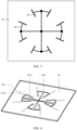
- FIG. 3 is a schematic diagram of a structure of an antenna assembly according to an embodiment of this application.
- the antenna assembly may include N elements 30, a feeding network 40, and a printed circuit board (printed circuit board, PCB) 50, where N is an integer greater than or equal to 3.
- the N elements 30 and the feeding network 40 are located on the PCB 50, the N elements 30 are all connected to the feeding network 40, each element 30 has a radial part, the radial part of each element 30 points to an antenna phase center, and a length of the radial part of each element is greater than a sum of lengths of other non-radial parts.
- N may be an even number or an odd number.
- N may be 3, or 4, or another value.
- a side lobe suppression capability of the antenna assembly is stronger when N is 4 than that when N is equal to 3.
- N is 8 is used as an example for description, but this does not constitute a limitation on a quantity of the elements 30 included in the antenna assembly.
- each element 30 After an electromagnetic wave radiated from each element is a distance away from the element, an equiphase surface of the electromagnetic wave approximates a spherical surface, and a spherical center of the spherical surface is the antenna phase center.
- each element 30 has a radial part pointing to the antenna phase center.
- each element 30 may not include other non-radial parts, that is, each element 30 is linear and points to the antenna phase center.
- each element 30 has a radial part pointing to the antenna phase center, and one or more other non-radial parts not pointing to the antenna phase center, and a sum of lengths of all non-radial parts not pointing to the antenna phase center is less than a length of the radial part included in each element 30.
- radiation intensity of an electromagnetic field, of each element, in a direction in which the radial part is located is greater than radiation intensity on a non-radial part, that is, a main radiation direction of each element is consistent with the direction in which the radial part is located. Therefore, each element 30 is equivalent to a line source, and has a relatively narrow beamwidth and an enhanced side lobe suppression capability.
- Each part of the element 30 may be linear or may have a width.
- a direction of one part of the element 30 refers to a direction of a major axis of the part.
- the element 30 has a width, and that the element is located in a radial direction means that a length direction of the element is in the radial direction.
- the width of the element 30 is not necessarily the same at different parts, provided that the width is generally smaller than the length and the length direction is in the radial direction.
- the N elements 30 may be distributed and arranged on a circumference centering on the antenna phase center.
- the elements 30 may be arranged at equal intervals on the circumference.
- an included angle between lines connecting two adjacent elements 30 to the antenna phase center is 360/N degrees.
- the N element pairs 30 may include a plurality of element pairs, and the two elements 30 in each element pair are centrosymmetrical with each other with respect to the antenna phase center.
- the included angle between the lines connecting the two adjacent elements 30 to the antenna phase center is 45 degrees.
- Eight elements 30 may be divided into four element pairs, and the two elements 30 in each element pair are centrosymmetrical with each other with respect to the antenna phase center.
- the element 30 may alternatively be arranged at unequal intervals. For example, it is assumed that an included angle between lines connecting two adjacent elements that are connected to both ends of a same transmission line in the feeding network 40 to the antenna phase center is a first included angle, an included angle between lines connecting two adjacent elements that are connected to different transmission lines to the antenna phase center is a second included angle, and the first included angle may be different from the second included angle.
- the N elements 30 and the feeding network 40 may be printed on a surface of the PCB 50, and the feeding network 40 and the N elements 30 may be located on an upper surface of the PCB 50 or a lower surface of the PCB 50 depending on differences of the feeding network 40 and of the N elements 30.
- the elements in the antenna assembly may be dipole elements, monopole elements, or slot elements. If the elements are different, the feeding network is different. Next, antenna assemblies including different elements and different feeding networks are described separately.
- each dipole element 301 includes two arms.
- One arm 3011 in the two arms is located on the upper surface of the PCB 50 and is connected to one end of an arc-shaped strip line that is located on the upper surface of the PCB 50 and that is in the double-sided parallel strip line power division network 401
- the other arm 3012 is located on the lower surface of the PCB 50 and is connected to one end of an arc-shaped strip line that is located on the lower surface of the PCB 50 and that is in the double-sided parallel strip line power division network
- the arc-shaped strip lines connected to the two arms are mirror-symmetrical with each other with respect to the PCB 50
- connection points between the two arms and the arc-shaped strip lines are mirror-symmetrical with each other with respect to the PCB 50.
- the double-sided parallel strip line power division network 401 includes an upper surface network and a lower surface network.
- the upper surface network is located on the upper surface of the PCB 50
- the lower surface network is located on the lower surface of the PCB 50
- the upper surface network and the lower surface network are mirror-symmetrical with each other with respect to a board of the PCB 50.
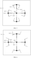
- FIG. 5 is a schematic diagram of an upper surface network located on the upper surface of the PCB 50 when N is an even number.
- the upper surface network may include a first power splitter 4011, a plurality of linear strip lines 4012, a plurality of impedance transformation lines 4013, a second power splitter 4014, and a plurality of arc-shaped strip lines 4015.
- the second power splitter 4014 may be a one-to-two power splitter, and the first power splitter 4011 may be selected based on a quantity of elements. For example, as shown in FIG.
- the quantity of elements is 8; when the second power splitter 4014 is a one-to-two power splitter, the first power splitter may be a one-to-four power splitter.
- the first power splitter 4011 of the feeding network may be located at the antenna phase center.
- a circumference corresponding to the feeding network may be determined by using a sum of lengths of the impedance transformation lines 4013 and the linear strip lines 4012 as a radius and using a position of the first power splitter 4011 as a center.
- the arc-shaped strip lines 4015 may be distributed along the circumference.
- a connection point between a dipole element and an arc-shaped strip line may be located on the circumference, that is, N dipole elements are distributed on the circumference centering on the antenna phase center.
- four output ports of the first power splitter 4011 may be connected to four impedance transformation lines 4013, the other end of each impedance transformation line 4013 is connected to one end of one linear strip line 4012, and impedance matching between the linear strip lines 4012 and the first power splitter 4011 may be implemented through the impedance transformation lines 4013.
- the second power splitter 4014 is connected to the other end of each linear strip line 4012. Two output ports of the second power splitter 4014 are respectively connected to an arc-shaped strip line 4015, and one end of each arc-shaped strip line 4015 may be connected to an arm 3011 of a dipole element 301.
- the first power splitter 4011 splits one current input to the feeding network into four currents
- the first power splitter may output the four currents through the four output ports, and the four currents are respectively transmitted to four second power splitters 4014 through four impedance transformation lines 4013 and four linear strip lines 4012 connected to the four impedance transformation lines 4013.
- Each second power splitter 4014 may split a received current into two currents and output the two currents through two output ports, and the two currents are respectively transmitted to arms of two adjacent dipole elements 301 through two arc-shaped strip lines 4015, to feed the two adjacent dipole elements 301.
- Each of eight dipole elements 301 has two arms.
- An arm 3011 in the two arms which is located in the circumference corresponding to the feeding network, is located on the upper surface and is connected to one end of one arc-shaped strip line 4015 in the upper surface network.
- a length of each arm may be a specified multiple of an operating wavelength of the antenna assembly. The specified multiple may be any value from 0.125 to 1.
- the impedance transformation lines 4013 may be quarter-wave impedance transformation lines, and the linear strip lines 4012 and the arc-shaped strip lines 4015 may be 50 ohm strip lines.
- FIG. 6 shows a lower surface network that is mirror-symmetrical with the upper surface network in FIG. 5 .
- the lower surface network also includes a first power splitter 4011, a plurality of linear strip lines 4012, a plurality of impedance transformation lines 4013, a second power splitter 4014, and a plurality of arc-shaped strip lines 4015.
- a structure of the lower surface network is the same as that of the upper surface network, and the lower surface network is located on the lower surface of the PCB 50 and is mirror-symmetrical with the upper surface network with respect to the PCB 50.
- For descriptions of components in the lower surface network refer to related descriptions of the upper surface network in FIG. 5 . Details are not described herein again in this embodiment of this application.
- the arm 3012 that is located outside the circumference corresponding to the feeding network and that is in the two arms of each of the eight dipole elements 301 is located on the lower surface of the PCB 50 and is connected to one end of one arc-shaped strip line 4015 in the lower surface network.
- the arms 3011 and 3012 that are respectively connected to two arc-shaped strip lines that are mirror-symmetrical with each other constitute a dipole element.
- the arm 3011 in FIG. 5 and the arm 3012 in FIG. 6 are two arms of one dipole element.
- the upper surface network and the lower surface network are mirror-symmetrical with each other, and the arc-shaped strip line 4015 connected to one arm 3011 in two arms of a same element and the arc-shaped strip line 4015 connected to the other arm 3012 are also mirror-symmetrical.
- connection points A and B of the two arms and the arc-shaped strip line are also mirror-symmetrical.
- the N dipole elements 301 may be divided into N/2 dipole element pairs.
- the two dipole elements in each dipole element pair may be centrosymmetrical with each other with respect to the antenna phase center. If two dipole elements that are radially symmetrical with each other are equivalent to a point source with an amplitude of 1 and a phase of 0, a function of radiation intensity F changing with a radiation angle ⁇ may be determined by the following formula (1).
- ⁇ is a pitch angle
- k is a propagation constant of an electromagnetic wave
- h is a distance between a PCB and a metal base plate located below the PCB
- a is a distance between the two dipole elements in a dipole element pair.
- a distance between the two dipole elements in a dipole element pair is adjusted, so that radiation intensity of the dipole element pair at different radiation angles may be adjusted, to adjust side lobe suppression capability of the antenna assembly.
- a distance between the two dipole elements in each dipole element pair that is included in the antenna assembly may be set based on a radiation angle of the dipole element pair and a required side lobe suppression capability.
- the distance between the two dipole elements in each dipole element pair may be a preset multiple of the operating wavelength of the antenna assembly.
- the preset multiple may be any value from 0.25 to 1.
- a distance between the first dipole element and the second dipole element may be a distance between a first connection point and a second connection point.
- the first connection point refers to a connection point between the first dipole element and the arc-shaped transmission line
- the second connection point refers to a connection point between the second dipole element and an arc-shaped strip line. That is, as shown in FIG. 5 and FIG. 6 , a distance between point A and point B is a distance between two dipole elements that are centrosymmetrical.
- N 8 is used as an example for description.
- N an even number
- the first power splitters included in the upper surface network and the lower surface network are different, and quantities of the impedance transformation lines and the strip lines included in the feeding network are also different.
- the first power splitter in the upper surface network and the lower surface network may be a one-to-three power splitter.
- the first power splitter may be connected to three impedance transformation lines, the three impedance transformation lines are connected to three linear strip lines, each linear strip line is connected to one one-to-two second power splitter, and each second power splitter may be connected to two arc-shaped strip lines.
- the feeding network is a double-sided parallel strip line power division network
- N is an even number.
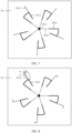
- the upper surface network located on the upper surface of the PCB 50 may include a first power splitter 4011, a plurality of impedance transformation lines 4013, and a plurality of odd-form strip lines 4016. As shown in FIG. 7 , for example, N is 5.
- the first power splitter 4011 may be a one-to-five power splitter, the first power splitter 4011 may be connected to five impedance transformation lines 4013, the other end of each impedance transformation line 4013 is connected to an odd-form strip line 4016, the odd-form strip line 4016 may be a strip line having an arc-shaped tail end as shown in FIG. 7 , and the tail end of each odd-form strip line 4016 may be connected to one arm 3011 of two arms in a dipole element 301.
- a structure of the lower surface network located on the lower surface of the PCB 50 is the same as that of the upper surface network, the lower surface network and the upper surface network are mirror-symmetrical with each other with respect to the PCB 50, and the other arm 3012 in the two arms in each dipole element 301 is connected to one end of one strip line in the lower surface network.
- the strip lines connected to the two arms of the dipole element are mirror-symmetrical with each other with respect to the PCB 50, so that connection points between the two arms and the strip lines are mirror-symmetrical with each other with respect to the PCB 50.
- the strip lines connected to the dipole element may not be arc-shaped strip lines but linear strip lines, and in this case, the linear strip lines may be tangent to the circumference corresponding to the feeding network.
- the two arms of each dipole element may be different in lengths and shapes.
- a length of the arm that is located outside the circumference corresponding to the feeding network and that is in the two arms may be smaller than a length of the other arm.
- the arm that is located within the circumference corresponding to the feeding network and that is in the two arms of the dipole element may be linear and point to the antenna phase center, and the other arm located outside the circumference corresponding to the feeding network may include a radial part and a non-radial part, for example, the tail end of the arm may be bent.
- the radial part is connected to an arc-shaped strip line, so that the radial part of the arm and another linear arm constitute a radial part of the dipole element.
- a length of the bent non-radial part is less than a sum of lengths of the radial part of the arm and the other arm.
- the arm located outside the circumference corresponding to the feeding network may be L-shaped. This is not limited in this embodiment of this application.
- FIG. 8 is a schematic diagram of an antenna assembly of which one arm of a dipole element is L-shaped.
- an arm 3011 is located within a circumference of the feeding network, and the arm 3011 may be linear and point to the antenna phase center.
- An arm 3012 is located outside the circumference corresponding to the feeding network, and the arm 3012 is L-shaped.
- the arm 3012 includes a radial part a and a non-radial part b, and the arm 3012 is connected to an arc-shaped strip line through the radial part a, so that the radial part a and the arm 3011 constitute a radial part of the dipole element.
- a length of the non-radial part b is less than a sum of lengths of the radial part a and the arm 3011.
- FIG. 8 is merely a possible implementation of the dipole element provided in this embodiment of this application.
- the arm located outside the circumference corresponding to the feeding network may be in another shape, and the arm located within the circumference corresponding to the feeding network may also be in another shape provided that a length of the radial part of the dipole element is greater than a sum of lengths of other non-radial parts.
- the N elements and the feeding network are located on the PCB, the N elements are all connected to the feeding network, each element has a radial part, the radial part of each element points to the antenna phase center, and a length of the radial part of each element is greater than a sum of lengths of other non-radial parts.
- radiation intensity of an electromagnetic field, of each element, in a direction in which the radial part is located is greater than radiation intensity on a non-radial part, that is, a main radiation direction of each element is consistent with the direction in which the radial part is located. Therefore, each element is equivalent to a line source, and has a relatively narrow beamwidth and an enhanced side lobe suppression capability.
- the N dipole elements may be divided into a plurality of dipole element pairs, and the two elements in each element pair are centrosymmetrical with each other with respect to the antenna phase center. In this way, when the antenna assembly is designed, a distance between two elements may be set based on a use scenario, so that radiation intensity of the antenna assembly at different radiation angles is adjusted, to further adjust a side lobe suppression capability of the antenna assembly.
- FIG. 9 is a schematic diagram of a structure of an antenna assembly that includes eight monopole elements.
- the antenna assembly includes eight monopole elements 302, a strip line power division network 402 and a PCB 50.
- the eight monopole elements 302 are all located on an upper surface of the PCB 50, and the strip line power division network 402 is also located on the upper surface of the PCB 50.
- Each monopole element 302 includes an arm.
- the strip line power division network 402 may include a first power splitter 4011, a plurality of linear strip lines 4012, a plurality of impedance transformation lines 4013, a second power splitter 4014, and a plurality of arc-shaped strip lines 4015.
- the first power splitter 4011 may be a one-to-four power splitter, quantities of the impedance transformation lines 4013 and the linear strip lines 4012 each may be 4, and a quantity of the arc-shaped strip lines 4015 is 8.
- the eight monopole elements may be linear, and the eight monopole elements point to an antenna phase center. In this case, other non-radial parts are not included in each monopole element.
- the first power splitter 4011 may be located at the antenna phase center, and a circumference corresponding to the feeding network may be determined by using a position of the first power splitter 4011 as a center of a circle.
- the arc-shaped strip lines 4015 may be distributed along the circumference. Connection points between the monopole elements and the arc-shaped strip lines may be located on the circumference, that is, N monopole elements are distributed on the circumference centering on the antenna phase center.
- the monopole elements 302 and the strip line power division network 402 are usually located on one side, for example, the upper surface, of the PCB 50. The other side of the PCB 50 may be provided with a base plate.
- the base plate may be circular or in any other shape. The base plate usually does not overlap with projections of the monopole elements 302.
- first power splitter 4011 Four output ports of the first power splitter 4011 are respectively connected to one ends of the four impedance transformation lines 4013, and the other ends of the four impedance transformation lines 4013 are respectively connected to one ends of the four linear strip lines 4012.
- the other end of each linear strip line 4012 is connected to one second power splitter 4014, and two output ports of the second power splitter 4014 are respectively connected to two arc-shaped strip lines 4015.
- the first power splitter may output the four currents through the four output ports, and the four currents are respectively transmitted to four second power splitters 4014 through the four impedance transformation lines 4013 and the four linear strip lines 4012 connected to the four impedance transformation lines 4013.
- Each second power splitter 4014 may split a received current into two currents and output the two currents through two output ports, and the two currents are respectively transmitted to two adjacent monopole elements 302 through two arc-shaped strip lines 4015, to feed the two adjacent monopole elements 302.
- the impedance transformation lines 4013 may be quarter-wave impedance transformation lines 4013, and the linear strip lines 4012 and the arc-shaped strip lines 4015 may be 50 ohm strip lines.
- the N monopole elements 302 may also be divided into N/2 element pairs, and the two monopole elements in each element pair are centrosymmetrical with each other with respect to the antenna phase center.
- the two elements in the element pair may be equivalent to a point source with an amplitude of 1 and a phase of 0, and correspondingly, a function of radiation intensity changing with a radiation angle ⁇ may also be expressed by the formula (1). Therefore, a distance between the two monopole elements in a monopole element pair is adjusted, so that radiation intensity of the monopole element pair at different radiation angles may be adjusted, to further adjust a side lobe suppression capability of the antenna assembly. That is, in this embodiment of this application, a distance between the two monopole elements in each monopole element pair that is included in the antenna assembly may be set based on a radiation angle of the monopole element pair and a required side lobe suppression capability.
- FIG. 9 an implementation of the antenna assembly that includes eight monopole elements is mainly described.
- N is another even number
- the first power splitter 4011 in the strip line power division network is different depending on a quantity of monopole elements, and quantities of the impedance transformation lines 4013 and the strip lines are different.
- the feeding network of the antenna assembly that includes an even number of dipole elements. Details are not described herein again in this embodiment of this application.
- N is an odd number
- N is an odd number
- each monopole element 302 may not be linear, for example, each monopole element 302 may be L-shaped.
- each monopole element 302 may include a radial part pointing to the antenna phase center and a non-radial part not pointing to the antenna phase center, where a length of the radial part is greater than that of the non-radial part.
- each monopole element 302 may alternatively be in another shape provided that the length of the radial part pointing to the antenna phase center is greater than that of other non-radial parts.
- N elements and the feeding network are located on the PCB, the N elements are all connected to the feeding network, each element has a radial part, the radial part of each element points to an antenna phase center, and a length of the radial part of each element is greater than a sum of lengths of other non-radial parts.
- radiation intensity of an electromagnetic field, of each element, in a direction in which the radial part is located is greater than radiation intensity on a non-radial part, that is, a main radiation direction of each element is consistent with the direction in which the radial part is located. Therefore, each element is equivalent to a line source, and has a relatively narrow beamwidth and an enhanced side lobe suppression capability.
- N dipole elements may be divided into a plurality of dipole element pairs, and the two elements in each element pair are centrosymmetrical with each other with respect to the antenna phase center. In this way, when the antenna assembly is designed, a distance between two elements may be set based on a use scenario, so that radiation intensity of the antenna assembly at different radiation angles is adjusted, to further adjust a side lobe suppression capability of the antenna assembly.
- the N elements included in the antenna assembly may alternatively be slot elements.
- the feeding network may be a strip line power division network.
- the N slot elements are located on the upper surface of the PCB and the strip line power division network is located on the lower surface of the PCB. This is different from a structure of the antenna assembly that includes monopole elements.
- FIG. 10 is a schematic diagram of a structure of an upper surface of a PCB of an antenna assembly that includes eight slot elements.
- the eight slot elements 303 refer to eight slots cut on the upper surface of the PCB 50, and each slot is a slot element.
- Each slot element 303 may be linear, and each slot element 303 points to an antenna phase center. That is, each slot element 303 does not include a non-radial part.
- FIG. 11 is a schematic diagram of a lower surface of the PCB 50 of the antenna assembly. As shown in FIG. 11 , a strip line power division network 402 is disposed on the lower surface of the PCB 50.
- the strip line power division network 402 may include a first power splitter 4011, a plurality of linear strip lines 4012, a plurality of impedance transformation lines 4013, a second power splitter 4014, and a plurality of odd-form strip lines 4016. Since the antenna assembly includes eight slot elements, the first power splitter 4011 may be a one-to-four power splitter, quantities of the impedance transformation lines 4013 and the linear strip lines 4012 each may be 4, and a quantity of the odd-form strip lines 4016 is 8.
- Each odd-form strip line 4016 may be an approximately L-shaped strip line obtained by connecting a section of linear strip line 4012 to a section of arc-shaped strip line, may be an arc-shaped strip line, or may be an L-shaped strip line obtained by connecting two linear strip lines 4012. Details are not described herein again in this embodiment of this application. In FIG. 10 , that each odd-form strip line 4016 is an approximately L-shaped strip line obtained by connecting a section of linear strip line to a section of arc-shaped strip line is used as an example for description.
- first power splitter 4011 Four output ports of the first power splitter 4011 are respectively connected to one ends of four impedance transformation lines 4013, and the other ends of the four impedance transformation lines 4013 are respectively connected to one ends of four linear strip lines 4012.
- the other end of each linear strip line 4012 is connected to one second power splitter 4014, and two output ports of the second power splitter 4014 are respectively connected to two odd-form strip lines 4016.
- the first power splitter may output the four currents through the four output ports, and the four currents are respectively transmitted to four second power splitters 4014 through the four impedance transformation lines 4013 and the four linear strip lines 4012 connected to the four impedance transformation lines 4013.
- Each second power splitter 4014 may split a received current into two currents and output the two currents through two output ports, and the two currents are respectively transmitted to two adjacent slot elements 303 through two odd-form strip lines 4016, to feed the two adjacent slot elements 303.
- the impedance transformation lines 4013 may be quarter-wave impedance transformation lines 4013, and the linear strip lines 4012 and the arc-shaped strip lines 4016 may be 50 ohm strip lines. This is not limited in this embodiment of this application.
- the upper surface of the PCB 50 may be a copper plate, the N slot elements 303 cut on the copper plate, and each slot intersects with an odd-form strip line 4016 on the lower surface of the PCB 50, so that each slot element 303 is connected to the odd-form strip line 4016.
- the N slot elements 303 may be divided into N/2 element pairs, and the two slot elements 303 in each element pair are centrosymmetrical with each other with respect to the antenna phase center. In this way, a distance between the two slot elements 303 in an element pair may be set, to adjust radiation intensity of the slot elements 303 at different radiation angles, to further adjust a side lobe suppression capability of the antenna assembly.
- N is another even number
- the first power splitter 4011 included in the strip line power division network 402 is different depending on a quantity of slot elements, and quantities of the impedance transformation lines 4013 and the strip lines are different.
- the feeding network of the antenna assembly that includes an even number of dipole elements. Details are not described herein again in this embodiment of this application.
- N is an odd number
- N is an odd number
- each slot element 303 may not be linear, for example, each slot element 303 may be L-shaped.
- each slot element 303 is not linear, refer to the foregoing related implementation in which the monopole element is not linear. Details are not described herein again in this embodiment of this application.
- the N elements and the feeding network are located on the PCB, the N elements are all connected to the feeding network, each element has a radial part, the radial part of each element points to the antenna phase center, and a length of the radial part of each element is greater than a sum of lengths of other non-radial parts.
- radiation intensity of an electromagnetic field, of each element, in a direction in which the radial part is located is greater than radiation intensity on a non-radial part, that is, a main radiation direction of each element is consistent with the direction in which the radial part is located. Therefore, each element is equivalent to a line source, and has a relatively narrow beamwidth and an enhanced side lobe suppression capability.
- N dipole elements may be divided into a plurality of dipole element pairs, and the two elements in each element pair are centrosymmetrical with each other with respect to the antenna phase center. In this way, when the antenna assembly is designed, a distance between two elements may be set based on a use scenario, so that radiation intensity of the antenna assembly at different radiation angles is adjusted, to further adjust a side lobe suppression capability of the antenna assembly.
Landscapes
- Engineering & Computer Science (AREA)
- Computer Networks & Wireless Communication (AREA)
- Variable-Direction Aerials And Aerial Arrays (AREA)
Claims (8)
- Antennenanordnung (205), wobei die Antennenanordnung N Elemente (30), ein Versorgungsnetzwerk (40) und eine Leiterplatte (PCB - Printed Circuit Board) (50), umfasst und N eine ganze Zahl größer oder gleich 3 ist; und
die N Elemente und das Versorgungsnetzwerk sich auf der Leiterplatte befinden, die N Elemente alle mit dem Versorgungsnetzwerk verbunden sind, wobei jedes Element Folgendes aufweist:einen radialen Teil; odereinen radialen Teil und nicht-radiale Teile, wobei eine Länge des radialen Teils jedes Elements größer ist als eine Summe der Längen der nicht-radialen Teile;wobei der radiale Teil jedes Elements auf ein Phasenzentrum der Antennenanordnung zeigt, und wobei das Versorgungsnetzwerk ein Leistungsteilungsnetzwerk mit doppelseitiger paralleler Streifenleitung (401) ist, dadurch gekennzeichnet, dass die N Elemente N Dipolelemente (301) sind; wobeijedes Dipolelement zwei Arme umfasst, einer (3011) der zwei Arme sich auf einer oberen Oberfläche der PCB befindet und mit einem Ende einer bogenförmigen Streifenleitung verbunden ist, das sich auf der oberen Oberfläche der PCB und in dem Leistungsteilungsnetzwerk mit doppelseitiger paralleler Streifenleitung befindet, der andere Arm (3012) sich auf einer unteren Oberfläche der PCB befindet und mit einem Ende einer bogenförmigen Streifenleitung verbunden ist, das sich auf der unteren Oberfläche der PCB und in dem Leistungsteilungsnetzwerk mit doppelseitiger paralleler Streifenleitung befindet, die mit den zwei Armen verbundenen bogenförmigen Streifenleitungen in Bezug auf die PCB spiegelsymmetrisch zueinander sind und Anschlusspunkte zwischen den zwei Armen und den bogenförmigen Streifenleitungen in Bezug auf die PCB spiegelsymmetrisch zueinander sind. - Antennenanordnung nach Anspruch 1, wobei N eine gerade Zahl ist, eine Vielzahl von Elementpaaren in den N Elemente ist und die Elemente in jedem Elementpaar in Bezug auf das Phasenzentrum der Antennenanordnung zueinander punktsymmetrisch sind.
- Antennenanordnung nach Anspruch 1, wobei das Leistungsteilungsnetzwerk mit doppelseitiger paralleler Streifenleitung ein oberes Oberflächennetzwerk und ein unteres Oberflächennetzwerk umfasst, wobei sich das obere Oberflächennetzwerk auf der oberen Oberfläche der PCB befindet, das untere Oberflächennetzwerk auf der unteren Oberfläche der PCB befindet und das obere Oberflächennetzwerk und das untere Oberflächennetzwerk in Bezug auf die PCB spiegelsymmetrisch zueinander sind; und
das obere Oberflächennetzwerk und das untere Oberflächennetzwerk jeweils einen ersten Leistungsteiler (4011), eine Vielzahl von linearen Streifenleitungen (4012), eine Vielzahl von Impedanztransformationsleitungen (4013), einen zweiten Leistungsteiler (4014) und eine Vielzahl von bogenförmigen Streifenleitungen (4015) umfassen, wobei der erste Leistungsteiler dazu konfiguriert ist, die Vielzahl von linearen Streifenleitungen und die Vielzahl von bogenförmigen Streifenleitungen zu verbinden, wobei jede der Vielzahl von linearen Streifenleitungen mit einer der Vielzahl von Impedanztransformationsleitungen verbunden ist, und der zweite Leistungsteiler dazu konfiguriert ist, die Vielzahl von Impedanztransformationsleitungen zu verbinden. - Antennenanordnung nach Anspruch 1 oder 3, wobei die Länge jedes der beiden Arme ein definiertes Vielfaches einer Betriebswellenlänge der Antennenanordnung beträgt.
- Antennenanordnung nach Anspruch 4, wobei das definierte Vielfache ein beliebiger Wert zwischen 0,125 und 1 ist.
- Antennenanordnung nach einem der Ansprüche 1 bis 5, wobei ein erster Arm der beiden Arme einen nicht radialen Teil umfasst, der erste Arm L-förmig ist, ein zweiter Arm keinen nicht radialen Teil umfasst und ein Abstand zwischen dem ersten Arm und dem Phasenzentrum der Antennenanordnung größer ist als ein Abstand zwischen dem zweiten Arm und dem Phasenzentrum der Antennenanordnung.
- Antennenanordnung nach einem der Ansprüche 1 bis 6, wobei sich ein Abstand zwischen einem ersten Dipolelement und einem zweiten Dipolelement, die in den N Dipolelementen punktsymmetrisch zueinander sind, auf einen Abstand zwischen einem ersten Anschlusspunkt und einem zweiten Anschlusspunkt bezieht, wobei der erste Anschlusspunkt ein Anschlusspunkt zwischen dem ersten Dipolelement und der bogenförmigen Streifenleitung ist und der zweite Anschlusspunkt ein Anschlusspunkt zwischen dem zweiten Dipolelement und der bogenförmigen Streifenleitung ist.
- Drahtlose Vorrichtung, wobei die drahtlose Vorrichtung eine Hochfrequenzschaltung (204) und die Antennenanordnung nach einem der Ansprüche 1 bis 7 umfasst; und
der Hochfrequenzschaltkreis dazu konfiguriert ist, zusammen mit der Antennenanordnung die Übertragung und den Empfang eines Funksignals zu ermöglichen.
Applications Claiming Priority (2)
| Application Number | Priority Date | Filing Date | Title |
|---|---|---|---|
| CN201911005244.8A CN111769372B (zh) | 2019-10-22 | 2019-10-22 | 天线组件和无线设备 |
| PCT/CN2020/088783 WO2021077718A1 (zh) | 2019-10-22 | 2020-05-06 | 天线组件和无线设备 |
Publications (3)
| Publication Number | Publication Date |
|---|---|
| EP4033609A1 EP4033609A1 (de) | 2022-07-27 |
| EP4033609A4 EP4033609A4 (de) | 2022-11-23 |
| EP4033609B1 true EP4033609B1 (de) | 2025-04-30 |
Family
ID=72718367
Family Applications (1)
| Application Number | Title | Priority Date | Filing Date |
|---|---|---|---|
| EP20878136.9A Active EP4033609B1 (de) | 2019-10-22 | 2020-05-06 | Antennenanordnung und und drahtlose vorrichtung |
Country Status (4)
| Country | Link |
|---|---|
| US (1) | US12368245B2 (de) |
| EP (1) | EP4033609B1 (de) |
| CN (1) | CN111769372B (de) |
| WO (1) | WO2021077718A1 (de) |
Families Citing this family (4)
| Publication number | Priority date | Publication date | Assignee | Title |
|---|---|---|---|---|
| WO2022120858A1 (zh) * | 2020-12-11 | 2022-06-16 | 华为技术有限公司 | 一种阵列天线及基站 |
| CN115189143B (zh) | 2021-04-07 | 2025-02-11 | 华为技术有限公司 | 可重构天线和网络设备 |
| CN113410642A (zh) * | 2021-06-09 | 2021-09-17 | 上海微波技术研究所(中国电子科技集团公司第五十研究所) | 宽带天线一分四功分馈电网络 |
| CN114421992B (zh) * | 2022-01-28 | 2023-10-31 | Oppo广东移动通信有限公司 | 射频前端模块、通信控制方法与装置、介质、电子设备 |
Family Cites Families (23)
| Publication number | Priority date | Publication date | Assignee | Title |
|---|---|---|---|---|
| GB2152757B (en) * | 1984-01-05 | 1987-10-14 | Plessey Co Plc | Antenna |
| US6147657A (en) * | 1998-05-19 | 2000-11-14 | Harris Corporation | Circular phased array antenna having non-uniform angular separations between successively adjacent elements |
| KR100526585B1 (ko) * | 2002-05-27 | 2005-11-08 | 삼성탈레스 주식회사 | 이중 편파 특성을 갖는 평판형 안테나 |
| US6954179B2 (en) * | 2003-11-06 | 2005-10-11 | Harris Corporation | Multiband radially distributed graded phased array antenna and associated methods |
| US20060189273A1 (en) * | 2005-02-18 | 2006-08-24 | U.S. Monolithics, L.L.C. | Systems, methods and devices for a ku/ka band transmitter-receiver |
| CN2836258Y (zh) * | 2005-08-05 | 2006-11-08 | 西安海天天线科技股份有限公司 | 一种改善低仰角性能的双频宽波束圆极化天线 |
| CN101997170A (zh) * | 2010-11-24 | 2011-03-30 | 东南大学 | 双节阻抗变换器馈电全向宽带偶极子阵列天线 |
| CN102122763A (zh) * | 2011-03-17 | 2011-07-13 | 东南大学 | 并联馈电的全向阵列天线 |
| US9259582B2 (en) * | 2011-04-29 | 2016-02-16 | Cyberonics, Inc. | Slot antenna for an implantable device |
| EP2727183B1 (de) * | 2011-06-30 | 2016-11-16 | Gapwaves AB | Verbesserte breitband-multidipolantenne mit frequenzunabhängigen strahlungseigenschaften |
| US9082307B2 (en) * | 2013-02-19 | 2015-07-14 | King Fahd University Of Petroleum And Minerals | Circular antenna array for vehicular direction finding |
| CN104037496B (zh) * | 2013-03-08 | 2016-03-16 | 上海贝尔股份有限公司 | 一种全向圆极化天线 |
| CN104157980B (zh) * | 2014-08-08 | 2017-02-15 | 电子科技大学 | 可重构微带八木天线 |
| US9478865B1 (en) * | 2014-12-18 | 2016-10-25 | L-3 Communications Corp. | Configurable horn antenna |
| CN205565000U (zh) * | 2016-04-26 | 2016-09-07 | 深圳前海智讯中联科技有限公司 | 一种多波束选择智能天线阵列及具有该天线阵列的系统 |
| CN106410397A (zh) * | 2016-10-27 | 2017-02-15 | 深圳国人通信股份有限公司 | 一种印刷偶极子振子 |
| CN106549233A (zh) * | 2016-12-07 | 2017-03-29 | 西安电子科技大学 | 超宽带水平极化全向连接型的维瓦尔第圆形阵列天线 |
| CN106785405A (zh) * | 2017-01-12 | 2017-05-31 | 重庆邮电大学 | 一种加载amc反射板的低剖面双极化偶极子基站天线 |
| CN107240783A (zh) * | 2017-06-07 | 2017-10-10 | 华中科技大学 | 一种双模式复用的涡旋电磁波天线 |
| CN107240766B (zh) * | 2017-06-09 | 2019-07-19 | 合肥工业大学 | 一种超宽带全金属圆极化天线单元 |
| TWI665827B (zh) * | 2018-02-07 | 2019-07-11 | 和碩聯合科技股份有限公司 | 天線裝置 |
| CN208014903U (zh) * | 2018-03-26 | 2018-10-26 | 安徽大学 | 一种适用于环境射频能量收集的天线 |
| CN110085966B (zh) * | 2019-04-29 | 2021-01-05 | 西安爱生无人机技术有限公司 | 一种地面遥测和遥控一体天线及平台 |
-
2019
- 2019-10-22 CN CN201911005244.8A patent/CN111769372B/zh active Active
-
2020
- 2020-05-06 EP EP20878136.9A patent/EP4033609B1/de active Active
- 2020-05-06 WO PCT/CN2020/088783 patent/WO2021077718A1/zh not_active Ceased
-
2022
- 2022-04-19 US US17/723,972 patent/US12368245B2/en active Active
Also Published As
| Publication number | Publication date |
|---|---|
| US12368245B2 (en) | 2025-07-22 |
| EP4033609A4 (de) | 2022-11-23 |
| CN111769372A (zh) | 2020-10-13 |
| WO2021077718A1 (zh) | 2021-04-29 |
| US20220247088A1 (en) | 2022-08-04 |
| EP4033609A1 (de) | 2022-07-27 |
| CN111769372B (zh) | 2021-10-22 |
Similar Documents
| Publication | Publication Date | Title |
|---|---|---|
| US12368245B2 (en) | Antenna assembly and wireless device | |
| US11239572B2 (en) | Beam-steering reconfigurable antenna arrays | |
| EP3859880B1 (de) | Endgerät | |
| US9954271B2 (en) | Radio-frequency device and wireless communication device for enhancing antenna isolation | |
| US20220399918A1 (en) | Apparatus that supports spatial diversity, at least at reception | |
| US9692119B2 (en) | Radio-frequency device and wireless communication device for enhancing antenna isolation | |
| JP7153133B2 (ja) | 端末装置用アンテナ | |
| CN111052507B (zh) | 一种天线及无线设备 | |
| CN109994815A (zh) | 一种电子设备及无线信号收发方法 | |
| US20230163462A1 (en) | Antenna device with improved radiation directivity | |
| WO2016054672A1 (en) | Stadium antenna | |
| WO2020174205A1 (en) | Dual polarised planar antenna, base station and method of manufacture | |
| CN112310655B (zh) | 电子设备 | |
| EP3852195B1 (de) | Antenne für endgerät | |
| EP2830151B1 (de) | Verfahren und System für mehrfache Einspeisepunktantennen | |
| US10892562B1 (en) | Multi-beam Yagi-based MIMO antenna system | |
| US12283756B2 (en) | Antenna array element with dual polarization, antenna array including antenna array element and electronic device including antenna array | |
| EP4340123A1 (de) | Kompakte und breitbandige strahlumschaltende gruppenantennenarchitektur | |
| EP4358296B1 (de) | Antenne und antennensystem | |
| EP3545586B1 (de) | Hochfrequenzmodulsignalsende-/-empfangsvorrichtung | |
| CN111403912B (zh) | 一种电子设备的盖体及电子设备 | |
| US11158952B1 (en) | Low profile omnidirectional antenna | |
| JP2005295188A (ja) | マルチビームアンテナ | |
| US20220131265A1 (en) | Electronic device | |
| CN108682960A (zh) | 多频阵列天线及通信系统 |
Legal Events
| Date | Code | Title | Description |
|---|---|---|---|
| STAA | Information on the status of an ep patent application or granted ep patent |
Free format text: STATUS: THE INTERNATIONAL PUBLICATION HAS BEEN MADE |
|
| PUAI | Public reference made under article 153(3) epc to a published international application that has entered the european phase |
Free format text: ORIGINAL CODE: 0009012 |
|
| STAA | Information on the status of an ep patent application or granted ep patent |
Free format text: STATUS: REQUEST FOR EXAMINATION WAS MADE |
|
| 17P | Request for examination filed |
Effective date: 20220420 |
|
| AK | Designated contracting states |
Kind code of ref document: A1 Designated state(s): AL AT BE BG CH CY CZ DE DK EE ES FI FR GB GR HR HU IE IS IT LI LT LU LV MC MK MT NL NO PL PT RO RS SE SI SK SM TR |
|
| A4 | Supplementary search report drawn up and despatched |
Effective date: 20221024 |
|
| RIC1 | Information provided on ipc code assigned before grant |
Ipc: H01Q 21/20 20060101ALI20221018BHEP Ipc: H01Q 21/00 20060101ALI20221018BHEP Ipc: H01Q 9/06 20060101ALI20221018BHEP Ipc: H01Q 1/22 20060101AFI20221018BHEP |
|
| DAV | Request for validation of the european patent (deleted) | ||
| DAX | Request for extension of the european patent (deleted) | ||
| REG | Reference to a national code |
Ref legal event code: R079 Free format text: PREVIOUS MAIN CLASS: H01Q0021200000 Ref country code: DE Ref legal event code: R079 Ref document number: 602020050605 Country of ref document: DE Free format text: PREVIOUS MAIN CLASS: H01Q0021200000 Ipc: H01Q0001220000 |
|
| GRAP | Despatch of communication of intention to grant a patent |
Free format text: ORIGINAL CODE: EPIDOSNIGR1 |
|
| STAA | Information on the status of an ep patent application or granted ep patent |
Free format text: STATUS: GRANT OF PATENT IS INTENDED |
|
| RIC1 | Information provided on ipc code assigned before grant |
Ipc: H01Q 21/20 20060101ALI20241202BHEP Ipc: H01Q 1/52 20060101ALI20241202BHEP Ipc: H01Q 21/00 20060101ALI20241202BHEP Ipc: H01Q 9/06 20060101ALI20241202BHEP Ipc: H01Q 1/22 20060101AFI20241202BHEP |
|
| INTG | Intention to grant announced |
Effective date: 20241223 |
|
| GRAS | Grant fee paid |
Free format text: ORIGINAL CODE: EPIDOSNIGR3 |
|
| GRAA | (expected) grant |
Free format text: ORIGINAL CODE: 0009210 |
|
| STAA | Information on the status of an ep patent application or granted ep patent |
Free format text: STATUS: THE PATENT HAS BEEN GRANTED |
|
| AK | Designated contracting states |
Kind code of ref document: B1 Designated state(s): AL AT BE BG CH CY CZ DE DK EE ES FI FR GB GR HR HU IE IS IT LI LT LU LV MC MK MT NL NO PL PT RO RS SE SI SK SM TR |
|
| REG | Reference to a national code |
Ref country code: CH Ref legal event code: EP Ref country code: GB Ref legal event code: FG4D |
|
| REG | Reference to a national code |
Ref country code: IE Ref legal event code: FG4D |
|
| REG | Reference to a national code |
Ref country code: DE Ref legal event code: R096 Ref document number: 602020050605 Country of ref document: DE |
|
| PGFP | Annual fee paid to national office [announced via postgrant information from national office to epo] |
Ref country code: DE Payment date: 20250507 Year of fee payment: 6 |
|
| REG | Reference to a national code |
Ref country code: NL Ref legal event code: MP Effective date: 20250430 |
|
| REG | Reference to a national code |
Ref country code: AT Ref legal event code: MK05 Ref document number: 1790975 Country of ref document: AT Kind code of ref document: T Effective date: 20250430 |
|
| PG25 | Lapsed in a contracting state [announced via postgrant information from national office to epo] |
Ref country code: PT Free format text: LAPSE BECAUSE OF FAILURE TO SUBMIT A TRANSLATION OF THE DESCRIPTION OR TO PAY THE FEE WITHIN THE PRESCRIBED TIME-LIMIT Effective date: 20250901 Ref country code: FI Free format text: LAPSE BECAUSE OF FAILURE TO SUBMIT A TRANSLATION OF THE DESCRIPTION OR TO PAY THE FEE WITHIN THE PRESCRIBED TIME-LIMIT Effective date: 20250430 Ref country code: ES Free format text: LAPSE BECAUSE OF FAILURE TO SUBMIT A TRANSLATION OF THE DESCRIPTION OR TO PAY THE FEE WITHIN THE PRESCRIBED TIME-LIMIT Effective date: 20250430 |
|
| REG | Reference to a national code |
Ref country code: LT Ref legal event code: MG9D |
|
| PG25 | Lapsed in a contracting state [announced via postgrant information from national office to epo] |
Ref country code: NO Free format text: LAPSE BECAUSE OF FAILURE TO SUBMIT A TRANSLATION OF THE DESCRIPTION OR TO PAY THE FEE WITHIN THE PRESCRIBED TIME-LIMIT Effective date: 20250730 Ref country code: GR Free format text: LAPSE BECAUSE OF FAILURE TO SUBMIT A TRANSLATION OF THE DESCRIPTION OR TO PAY THE FEE WITHIN THE PRESCRIBED TIME-LIMIT Effective date: 20250731 |
|
| PG25 | Lapsed in a contracting state [announced via postgrant information from national office to epo] |
Ref country code: NL Free format text: LAPSE BECAUSE OF FAILURE TO SUBMIT A TRANSLATION OF THE DESCRIPTION OR TO PAY THE FEE WITHIN THE PRESCRIBED TIME-LIMIT Effective date: 20250430 Ref country code: PL Free format text: LAPSE BECAUSE OF FAILURE TO SUBMIT A TRANSLATION OF THE DESCRIPTION OR TO PAY THE FEE WITHIN THE PRESCRIBED TIME-LIMIT Effective date: 20250430 |
|
| PG25 | Lapsed in a contracting state [announced via postgrant information from national office to epo] |
Ref country code: BG Free format text: LAPSE BECAUSE OF FAILURE TO SUBMIT A TRANSLATION OF THE DESCRIPTION OR TO PAY THE FEE WITHIN THE PRESCRIBED TIME-LIMIT Effective date: 20250430 |
|
| PG25 | Lapsed in a contracting state [announced via postgrant information from national office to epo] |
Ref country code: HR Free format text: LAPSE BECAUSE OF FAILURE TO SUBMIT A TRANSLATION OF THE DESCRIPTION OR TO PAY THE FEE WITHIN THE PRESCRIBED TIME-LIMIT Effective date: 20250430 |
|
| PG25 | Lapsed in a contracting state [announced via postgrant information from national office to epo] |
Ref country code: AT Free format text: LAPSE BECAUSE OF FAILURE TO SUBMIT A TRANSLATION OF THE DESCRIPTION OR TO PAY THE FEE WITHIN THE PRESCRIBED TIME-LIMIT Effective date: 20250430 |
|
| PG25 | Lapsed in a contracting state [announced via postgrant information from national office to epo] |
Ref country code: RS Free format text: LAPSE BECAUSE OF FAILURE TO SUBMIT A TRANSLATION OF THE DESCRIPTION OR TO PAY THE FEE WITHIN THE PRESCRIBED TIME-LIMIT Effective date: 20250731 |
|
| PG25 | Lapsed in a contracting state [announced via postgrant information from national office to epo] |
Ref country code: IS Free format text: LAPSE BECAUSE OF FAILURE TO SUBMIT A TRANSLATION OF THE DESCRIPTION OR TO PAY THE FEE WITHIN THE PRESCRIBED TIME-LIMIT Effective date: 20250830 |
|
| PG25 | Lapsed in a contracting state [announced via postgrant information from national office to epo] |
Ref country code: LV Free format text: LAPSE BECAUSE OF FAILURE TO SUBMIT A TRANSLATION OF THE DESCRIPTION OR TO PAY THE FEE WITHIN THE PRESCRIBED TIME-LIMIT Effective date: 20250430 |
|
| REG | Reference to a national code |
Ref country code: CH Ref legal event code: H13 Free format text: ST27 STATUS EVENT CODE: U-0-0-H10-H13 (AS PROVIDED BY THE NATIONAL OFFICE) Effective date: 20251223 |
|
| PG25 | Lapsed in a contracting state [announced via postgrant information from national office to epo] |
Ref country code: DK Free format text: LAPSE BECAUSE OF FAILURE TO SUBMIT A TRANSLATION OF THE DESCRIPTION OR TO PAY THE FEE WITHIN THE PRESCRIBED TIME-LIMIT Effective date: 20250430 Ref country code: SM Free format text: LAPSE BECAUSE OF FAILURE TO SUBMIT A TRANSLATION OF THE DESCRIPTION OR TO PAY THE FEE WITHIN THE PRESCRIBED TIME-LIMIT Effective date: 20250430 |
|
| PG25 | Lapsed in a contracting state [announced via postgrant information from national office to epo] |
Ref country code: LU Free format text: LAPSE BECAUSE OF NON-PAYMENT OF DUE FEES Effective date: 20250506 |
|
| PG25 | Lapsed in a contracting state [announced via postgrant information from national office to epo] |
Ref country code: CH Free format text: LAPSE BECAUSE OF NON-PAYMENT OF DUE FEES Effective date: 20250531 |
|
| PG25 | Lapsed in a contracting state [announced via postgrant information from national office to epo] |
Ref country code: CZ Free format text: LAPSE BECAUSE OF FAILURE TO SUBMIT A TRANSLATION OF THE DESCRIPTION OR TO PAY THE FEE WITHIN THE PRESCRIBED TIME-LIMIT Effective date: 20250430 |
|
| PG25 | Lapsed in a contracting state [announced via postgrant information from national office to epo] |
Ref country code: EE Free format text: LAPSE BECAUSE OF FAILURE TO SUBMIT A TRANSLATION OF THE DESCRIPTION OR TO PAY THE FEE WITHIN THE PRESCRIBED TIME-LIMIT Effective date: 20250430 |
|
| PG25 | Lapsed in a contracting state [announced via postgrant information from national office to epo] |
Ref country code: SK Free format text: LAPSE BECAUSE OF FAILURE TO SUBMIT A TRANSLATION OF THE DESCRIPTION OR TO PAY THE FEE WITHIN THE PRESCRIBED TIME-LIMIT Effective date: 20250430 |
|
| PG25 | Lapsed in a contracting state [announced via postgrant information from national office to epo] |
Ref country code: IT Free format text: LAPSE BECAUSE OF FAILURE TO SUBMIT A TRANSLATION OF THE DESCRIPTION OR TO PAY THE FEE WITHIN THE PRESCRIBED TIME-LIMIT Effective date: 20250430 |
|
| REG | Reference to a national code |
Ref country code: BE Ref legal event code: MM Effective date: 20250531 |
|
| PG25 | Lapsed in a contracting state [announced via postgrant information from national office to epo] |
Ref country code: MC Free format text: LAPSE BECAUSE OF FAILURE TO SUBMIT A TRANSLATION OF THE DESCRIPTION OR TO PAY THE FEE WITHIN THE PRESCRIBED TIME-LIMIT Effective date: 20250430 |
|
| REG | Reference to a national code |
Ref country code: DE Ref legal event code: R097 Ref document number: 602020050605 Country of ref document: DE |
|
| PG25 | Lapsed in a contracting state [announced via postgrant information from national office to epo] |
Ref country code: RO Free format text: LAPSE BECAUSE OF FAILURE TO SUBMIT A TRANSLATION OF THE DESCRIPTION OR TO PAY THE FEE WITHIN THE PRESCRIBED TIME-LIMIT Effective date: 20250430 |
|
| PLBE | No opposition filed within time limit |
Free format text: ORIGINAL CODE: 0009261 |
|
| STAA | Information on the status of an ep patent application or granted ep patent |
Free format text: STATUS: NO OPPOSITION FILED WITHIN TIME LIMIT |
|
| REG | Reference to a national code |
Ref country code: CH Ref legal event code: L10 Free format text: ST27 STATUS EVENT CODE: U-0-0-L10-L00 (AS PROVIDED BY THE NATIONAL OFFICE) Effective date: 20260311 |
|
| GBPC | Gb: european patent ceased through non-payment of renewal fee |
Effective date: 20250730 |