EP4031802B1 - Led filament lampe - Google Patents
Led filament lampe Download PDFInfo
- Publication number
- EP4031802B1 EP4031802B1 EP20771297.7A EP20771297A EP4031802B1 EP 4031802 B1 EP4031802 B1 EP 4031802B1 EP 20771297 A EP20771297 A EP 20771297A EP 4031802 B1 EP4031802 B1 EP 4031802B1
- Authority
- EP
- European Patent Office
- Prior art keywords
- led filament
- encapsulant
- led
- maxima
- light
- Prior art date
- Legal status (The legal status is an assumption and is not a legal conclusion. Google has not performed a legal analysis and makes no representation as to the accuracy of the status listed.)
- Active
Links
Images

Classifications
-
- F—MECHANICAL ENGINEERING; LIGHTING; HEATING; WEAPONS; BLASTING
- F21—LIGHTING
- F21K—NON-ELECTRIC LIGHT SOURCES USING LUMINESCENCE; LIGHT SOURCES USING ELECTROCHEMILUMINESCENCE; LIGHT SOURCES USING CHARGES OF COMBUSTIBLE MATERIAL; LIGHT SOURCES USING SEMICONDUCTOR DEVICES AS LIGHT-GENERATING ELEMENTS; LIGHT SOURCES NOT OTHERWISE PROVIDED FOR
- F21K9/00—Light sources using semiconductor devices as light-generating elements, e.g. using light-emitting diodes [LED] or lasers
- F21K9/20—Light sources comprising attachment means
- F21K9/23—Retrofit light sources for lighting devices with a single fitting for each light source, e.g. for substitution of incandescent lamps with bayonet or threaded fittings
- F21K9/232—Retrofit light sources for lighting devices with a single fitting for each light source, e.g. for substitution of incandescent lamps with bayonet or threaded fittings specially adapted for generating an essentially omnidirectional light distribution, e.g. with a glass bulb
-
- F—MECHANICAL ENGINEERING; LIGHTING; HEATING; WEAPONS; BLASTING
- F21—LIGHTING
- F21K—NON-ELECTRIC LIGHT SOURCES USING LUMINESCENCE; LIGHT SOURCES USING ELECTROCHEMILUMINESCENCE; LIGHT SOURCES USING CHARGES OF COMBUSTIBLE MATERIAL; LIGHT SOURCES USING SEMICONDUCTOR DEVICES AS LIGHT-GENERATING ELEMENTS; LIGHT SOURCES NOT OTHERWISE PROVIDED FOR
- F21K9/00—Light sources using semiconductor devices as light-generating elements, e.g. using light-emitting diodes [LED] or lasers
- F21K9/20—Light sources comprising attachment means
- F21K9/23—Retrofit light sources for lighting devices with a single fitting for each light source, e.g. for substitution of incandescent lamps with bayonet or threaded fittings
- F21K9/235—Details of bases or caps, i.e. the parts that connect the light source to a fitting; Arrangement of components within bases or caps
-
- F—MECHANICAL ENGINEERING; LIGHTING; HEATING; WEAPONS; BLASTING
- F21—LIGHTING
- F21K—NON-ELECTRIC LIGHT SOURCES USING LUMINESCENCE; LIGHT SOURCES USING ELECTROCHEMILUMINESCENCE; LIGHT SOURCES USING CHARGES OF COMBUSTIBLE MATERIAL; LIGHT SOURCES USING SEMICONDUCTOR DEVICES AS LIGHT-GENERATING ELEMENTS; LIGHT SOURCES NOT OTHERWISE PROVIDED FOR
- F21K9/00—Light sources using semiconductor devices as light-generating elements, e.g. using light-emitting diodes [LED] or lasers
- F21K9/20—Light sources comprising attachment means
- F21K9/23—Retrofit light sources for lighting devices with a single fitting for each light source, e.g. for substitution of incandescent lamps with bayonet or threaded fittings
- F21K9/238—Arrangement or mounting of circuit elements integrated in the light source
-
- F—MECHANICAL ENGINEERING; LIGHTING; HEATING; WEAPONS; BLASTING
- F21—LIGHTING
- F21K—NON-ELECTRIC LIGHT SOURCES USING LUMINESCENCE; LIGHT SOURCES USING ELECTROCHEMILUMINESCENCE; LIGHT SOURCES USING CHARGES OF COMBUSTIBLE MATERIAL; LIGHT SOURCES USING SEMICONDUCTOR DEVICES AS LIGHT-GENERATING ELEMENTS; LIGHT SOURCES NOT OTHERWISE PROVIDED FOR
- F21K9/00—Light sources using semiconductor devices as light-generating elements, e.g. using light-emitting diodes [LED] or lasers
- F21K9/60—Optical arrangements integrated in the light source, e.g. for improving the colour rendering index or the light extraction
- F21K9/64—Optical arrangements integrated in the light source, e.g. for improving the colour rendering index or the light extraction using wavelength conversion means distinct or spaced from the light-generating element, e.g. a remote phosphor layer
-
- H—ELECTRICITY
- H10—SEMICONDUCTOR DEVICES; ELECTRIC SOLID-STATE DEVICES NOT OTHERWISE PROVIDED FOR
- H10W—GENERIC PACKAGES, INTERCONNECTIONS, CONNECTORS OR OTHER CONSTRUCTIONAL DETAILS OF DEVICES COVERED BY CLASS H10
- H10W90/00—Package configurations
-
- F—MECHANICAL ENGINEERING; LIGHTING; HEATING; WEAPONS; BLASTING
- F21—LIGHTING
- F21Y—INDEXING SCHEME ASSOCIATED WITH SUBCLASSES F21K, F21L, F21S and F21V, RELATING TO THE FORM OR THE KIND OF THE LIGHT SOURCES OR OF THE COLOUR OF THE LIGHT EMITTED
- F21Y2103/00—Elongate light sources, e.g. fluorescent tubes
- F21Y2103/10—Elongate light sources, e.g. fluorescent tubes comprising a linear array of point-like light-generating elements
-
- F—MECHANICAL ENGINEERING; LIGHTING; HEATING; WEAPONS; BLASTING
- F21—LIGHTING
- F21Y—INDEXING SCHEME ASSOCIATED WITH SUBCLASSES F21K, F21L, F21S and F21V, RELATING TO THE FORM OR THE KIND OF THE LIGHT SOURCES OR OF THE COLOUR OF THE LIGHT EMITTED
- F21Y2115/00—Light-generating elements of semiconductor light sources
- F21Y2115/10—Light-emitting diodes [LED]
-
- H—ELECTRICITY
- H10—SEMICONDUCTOR DEVICES; ELECTRIC SOLID-STATE DEVICES NOT OTHERWISE PROVIDED FOR
- H10H—INORGANIC LIGHT-EMITTING SEMICONDUCTOR DEVICES HAVING POTENTIAL BARRIERS
- H10H20/00—Individual inorganic light-emitting semiconductor devices having potential barriers, e.g. light-emitting diodes [LED]
- H10H20/80—Constructional details
- H10H20/85—Packages
- H10H20/851—Wavelength conversion means
- H10H20/8514—Wavelength conversion means characterised by their shape, e.g. plate or foil
-
- H—ELECTRICITY
- H10—SEMICONDUCTOR DEVICES; ELECTRIC SOLID-STATE DEVICES NOT OTHERWISE PROVIDED FOR
- H10H—INORGANIC LIGHT-EMITTING SEMICONDUCTOR DEVICES HAVING POTENTIAL BARRIERS
- H10H20/00—Individual inorganic light-emitting semiconductor devices having potential barriers, e.g. light-emitting diodes [LED]
- H10H20/80—Constructional details
- H10H20/85—Packages
- H10H20/852—Encapsulations
- H10H20/853—Encapsulations characterised by their shape
-
- H—ELECTRICITY
- H10—SEMICONDUCTOR DEVICES; ELECTRIC SOLID-STATE DEVICES NOT OTHERWISE PROVIDED FOR
- H10H—INORGANIC LIGHT-EMITTING SEMICONDUCTOR DEVICES HAVING POTENTIAL BARRIERS
- H10H20/00—Individual inorganic light-emitting semiconductor devices having potential barriers, e.g. light-emitting diodes [LED]
- H10H20/80—Constructional details
- H10H20/882—Scattering means
Definitions
- the present invention relates to a LED filament lamp which comprises at least one LED filament.
- the present invention further relates to a luminaire comprising a reflector and said LED filament lamp.
- LED light emitting diodes
- LED-based lighting solutions there is currently a very large interest in lighting devices and/or arrangements (such as lamps) provided with LEDs, and incandescent lamps are rapidly being replaced by LED-based lighting solutions. It is nevertheless appreciated and desired to have retrofit lighting devices (e.g. lamps) which have the look of an incandescent lamp. For this purpose, it is possible to make use of the infrastructure for producing incandescent lamps based on LED filaments arranged in such a bulb. However, the light generated by LED filament lamps may, for some applications, appear static, "cold" and/or unattractive.
- Candles are able to generate light which is highly attractive and appealing. Light emitted from the open flame of a candle may, compared to light emitted from LEDs and/or incandescent lamps, appear more vivid, sparkling, "warm”, aesthetic and/or romantic. However, one of the major disadvantages of the use of candles is the risk of fire associated with an open flame.
- US 2019/0113181 A1 discloses a filament which includes a multiplicity of light-emitting semiconductor chips, wherein the semiconductor chips are arranged on a carrier, the semiconductor chips being electrically contacted, a scattering structure is configured to scatter light of the light-emitting semiconductor chips, the scattering structure is formed by structuring a surface, a converter covers the light-emitting semiconductor chips, and the structuring of the surface is formed on a surface of the converter.
- DE 10 2016 105211 A1 discloses a filament with a radiation-permeable substrate, a plurality of light-emitting diodes (LEDs) and a converter layer.
- the LEDs being arranged on the substrate and the converter layer covering the LEDs and the substrate.
- the converter layer on an upper side of the substrate has a first partial layer and a second partial layer on an underside of the substrate.
- the converter layer is set up to achieve an improved radiation profile of the filament such that - the converter layer has a varying vertical layer thickness along a lateral direction, and/or - the first partial layer and the second partial layer differentiate from one another with regard to their geometry and/or their material composition.
- US 2018/045379 A1 discloses an LED filament.
- the LED filament includes LED chips, two conductive electrodes, conductive wires, an enclosure coating, and one or more auxiliary piece.
- the LED chips are arranged in an array and electrically connected with one another.
- the two conductive electrodes are corresponding to the array.
- Each of the two conductive electrodes is electrically connected to a corresponding LED chip at an end of the array.
- the conductive wires electrically connect the LED chips and the two conductive electrodes.
- the conductive wires are respectively between every two adjacent LED chips of the array and between each of the two conductive electrodes and the corresponding LED chip at an end of the array.
- the enclosure coating is on two or more sides of the array and the two conductive electrodes.
- each of the two conductive electrodes is exposed from the enclosure.
- the auxiliary piece is disposed in the enclosure coating and overlaps one of the conductive wires between each of the two conductive electrodes and the corresponding one of the two LED chips respectively at two ends of the array on a radial direction of the LED filament.
- the LED filament comprises at least one LED section, a conductive section, two conductive electrodes and a light conversion layer.
- the conductive section is used to electrically connect two adjacent LED sections.
- the two conductive electrodes are electrically connected to each of the LED sections.
- Each of the LED sections includes at least two LED chips electrically connected to each other.
- the light conversion layer covers the LED sections, the conductive sections and the conductive electrodes, and a part of the two electrodes is exposed respectively. Since the LED filament includes the LED section and the conductive section, when the LED filament is bent, the stress is easily concentrated on the conductive section. Therefore, the breakage probability of the conductive wires connected within the LED section is reduced during bending. The quality of the LED filament and its application is improved.
- the optoelectronic semiconductor chip has the following features: a semiconductor layer sequence with a plurality of pixels which has an active layer which is suitable for generating electromagnetic radiation of a first wavelength range, and a large number of conversion elements, each conversion element being suitable for converting radiation of the first wavelength range into radiation of a second wavelength range. Each pixel having a radiation exit area and a conversion element on each radiation exit area is arranged. Each conversion element has a greater thickness in a central area than in an edge area. Furthermore, a method for producing an optoelectronic semiconductor chip and a headlight with an optoelectronic semiconductor chip are described.
- a LED filament lamp provides LED filament lamp light and comprises at least one LED filament.
- the at least one LED filament has a LED filament length.
- the at least one LED filament provides LED filament light and comprises an array of a plurality of LEDs and an encapsulant.
- the array of the plurality of LEDs provides LED light and extends along the LED filament length.
- the encapsulant at least partially encloses the plurality of LEDs.
- the encapsulant comprises a light scattering material.
- At least one of (i) the thickness of the encapsulant, and (ii) the concentration of the light scattering material in the encapsulant, along the LED filament length increases over at least two adjacent first LEDs and decreases over at least two adjacent second LEDs different from the at least two adjacent first LEDs.
- the thickness and/or concentration firstly increases and secondly decreases at least along a portion of the LED filament length.
- the present invention is based on the idea of providing a LED filament lamp wherein the appearance of the LED filament(s) of the LED filament lamp and/or the light emitted from the LED filament lamp during its operation may resemble or mimic that of a candle. Furthermore, by the features of the LED filament lamp, the lamp is furthermore able to combine one or more of the numerous advantages of LED lighting devices with the attractiveness and the appealing properties of light emitted from a candle.
- the present invention is advantageous in that properties of the LED filament(s) of the LED filament lamp may lead to a generation of light which may resemble or mimic the relatively vivid, sparkling, "warm”, aesthetic and/or romantic light of an open flame of a candle.
- the reason is that the LED filament has a variable diffuser along the length of the LED filament.
- the present invention is further advantageous in that the LED filament lamp may combine the aesthetic features of candlelight with the incontestable safety of operating an electric light compared to that of a light source having an open flame.
- the present invention is further advantageous in that the LED filament lamp has a much longer operational life compared to that of a candle. Hence, it is much more convenient and/or cost-efficient to operate a LED filament lamp instead of a candle.
- the LED filament lamp of the present invention furthermore comprises relatively few components.
- the low number of components is advantageous in that the LED filament lamp is relatively inexpensive to fabricate.
- the low number of components of the LED filament lamp implies an easier recycling, especially compared to devices or arrangements comprising a relatively high number of components which impede an easy disassembling and/or recycling operation.
- the light intensity of the LED filament light decreases and increases respectively over said first LEDs and said second LEDs at least along a portion of the LED filament length (L), such that the light intensity (LI) of the LED filament light (101') varies along said portion of the LED filament length (L).
- the light intensity may be defined as the number of photons per area.
- a LED filament (lamp), for example, disclosed in US 2019/0113181 A1 is unable to provide decorative lighting with improved decorative look and/or appearance. The reason is that the light emitted from such a LED filament does not vary along said portion (from one LED area to another LED area) of the LED filament length (L).
- the at least one LED filament may comprise a carrier e.g. a substrate.
- the array of the plurality of LEDs may be arranged on a first surface of the carrier.
- an array of a plurality of LEDs may be arranged on a second surface of the carrier, opposite to said first surface.
- an encapsulant is arranged on the second surface of the carrier.
- an encapsulant may at least partly cover an array of a plurality of LEDs which may be arranged on a second surface of the carrier.
- the substrate may be flexible or rigid.
- a rigid substrate may be made from glass, quarts, sapphire and/or a polymer.
- a flexible substrate may be made from a polymer such as for example of poly imide.
- a rigid substrate provides strength and rigidly mounting of the at least one LED filament.
- a flexible substrate provides flexibility and flexible mounting of the at least one LED filament.
- the substrate is light transmissive such as translucent and preferably transparent to enable high light transmission through the substrate.
- the encapsulant comprises a light scattering material.
- light scattering material it is here meant a material, composition and/or substance which is configured to scatter and/or reflect light.
- the light scattering material does not convert light and does (substantially) not absorb light (at least less than 5%).
- the light scattering material may comprise gas bubbles and/or scattering particles such as for example Al2O3, BaSO4, TiO2 and/or particles having a different.
- the LED filament lamp comprises at least one LED filament.
- the at least one LED filament in its turn, comprises an array of LEDs.
- array it is here meant a linear arrangement or chain of LEDs, or the like, arranged in the LED filament(s).
- the LEDs may furthermore be arranged, mounted and/or mechanically coupled on/to a carrier e.g. a substrate of each LED filament, wherein the substrate is configured to support the LEDs.
- the array of LEDs may comprise a luminescent converter.
- the luminescent converter at least partially covers the LEDs.
- the luminescent converter may also at least partly or fully cover a carrier which may carry the array of LEDs.
- the luminescent converter may also cover at least part of the first mayor surface of the carrier.
- the luminescent converter may also cover at least part of the second mayor surface of the carrier.
- the luminescent converter comprises a luminescent material.
- luminescent material it is here meant a material, composition and/or substance which is configured to emit light under external energy excitation.
- the luminescent material may an inorganic phosphor, organic phosphor and/or quantum dots/rods.
- the LED filament(s) further comprises an encapsulant at least partially or fully enclosing the plurality of LEDs.
- encapsulant it is here meant a material, element, arrangement, or the like, which is configured or arranged to at least partially surround, encapsulate and/or enclose the plurality of LEDs of the LED filament(s).
- the LED filament may further comprise a luminescent converter.
- the LED filament lamp has the feature that said increase and/or decrease in thickness of the encapsulant and/or concentration of the light scattering material in the encapsulant is gradual.
- the obtained effect is that the LED filament lamp provides an improved attractive and appealing light effect.
- the reason is that there are gradual changes in intensity along the LED filament length. Gradual means taking place or progressing slowly or by degrees, for example continuously or by small steps.
- the LED filament lamp may have the feature that the LED filament comprises a luminescent converter.
- the luminescent converter at least partly covers the array of the plurality of LEDs.
- the luminescent converter is arranged between the encapsulant and the array of the plurality of LEDs.
- the luminescent converter is configured to at least partly convert LED light into converted light.
- the LED filament lamp may have the feature that the luminescent converter is provided as a continuous layer over the array of the plurality of LEDs.
- the LED filament lamp may have the feature that the plurality of LEDs are phosphor converted (pc) LEDs.
- the pc-LEDs may emit white light.
- the LEDs may be blue LEDs comprising a yellow/green and a red phosphor for partially converting blue LED light into green/yellow light and red light.
- the LEDs may be UV LEDs comprising a blue, yellow/green and a red phosphor for partially/fully converting UV LED light into blue light and green/yellow light and red light.
- the LED filament lamp may have the feature that the plurality of LEDs are colored LEDs.
- the colored LEDs may, in total, emit white light.
- the plurality of LEDs may comprise blue, green and red LEDs.
- the LED filament lamp has the feature that the LED filament comprises a plurality of subsequent increases and decreases in thickness of the encapsulant and/or concentration of the light scattering material in the encapsulant which form a plurality of maxima in said thicknesses and/or said concentrations along LED filament length.
- the obtained effect is that the LED filament lamp provides an improved attractive and appealing light effect. The reason is that there are multiple changes in intensity along the LED filament length.
- the maxima has a maxima height and between the maxima there may be minima which have a minima height.
- the maxima height is at least 1.7 times the minima height.
- the maxima may have a maxima concentration and between the maxima there may be minima which have a minima concentration.
- the maxima concentration is at least 1.7 times the minima concentration.
- the LED filament lamp may have the feature that the distance between said maxima is varied along the LED filament length.
- the obtained effect is that the LED filament lamp provides an improved attractive and appealing light effect. The reason is that the distances between high intensity areas are different.
- the LED filament lamp may have the feature that the distance between said maxima (M) is randomly varied along the LED filament length.
- M the distance between said maxima
- the LED filament lamp may have the feature that said maxima have different thicknesses of the encapsulant and/or concentrations of the light scattering material in the encapsulant along LED filament length.
- the obtained effect is that the LED filament lamp provides an improved attractive and appealing light effect. The reason is that the high and low intensity areas have a different intensity.
- the LED filament lamp may have the feature that the distance between said maxima is varied along the LED filament length, and wherein said maxima have different thicknesses of the encapsulant and/or concentrations of the light scattering material in the encapsulant along the LED filament length.
- the obtained effect is that the LED filament lamp provides a further improved attractive and appealing light effect. The reason is that a combination of both measures is used.
- the LED filament lamp may have the feature that the number of said maxima is at least 5.
- the obtained effect is that the LED filament lamp provides an improved attractive and appealing light effect. The reason is that there are multiple high and low intensity areas.
- the LED filament lamp may have the feature that the thickness of the encapsulant and/or concentration of the light scattering material in the encapsulant of at least three maxima are different.
- the obtained effect is that the LED filament lamp provides an improved attractive and appealing light effect.
- the LED filament lamp is more attractive/pleasant to look at.
- the reason is that there are multiple high and low intensity areas which have a different intensity. This leads to a generation of light which resemble or mimic a sparkling flame of a candle.
- the LED filament lamp may have the feature that the thickness of the encapsulant and/or concentration of the light scattering material in the encapsulant of at least five maxima are different.
- the LED filament lamp may have the feature that the LED filament may have at least four maxima M and at least three different distances between said maxima.
- the LED filament lamp has the feature that the LED filament may have at least three maxima M which have different thicknesses T L of the encapsulant 104 and/or concentrations C L of the light scattering material 105 in the encapsulant 104 along the LED filament length L.
- the LED filament lamp has the feature that at least one of the thickness of the encapsulant and the concentration of the light scattering material in the encapsulant increases and/or decreases non-linearly.
- the obtained effect is that the LED filament lamp provides an improved attractive and appealing light effect.
- the reason is that non-linear intensity profiles are obtained along the length of the LED filament.
- the LED filament lamp may have the feature that the at least one LED filament comprises a first LED filament and a second LED filament.
- the obtained effect is that the LED filament lamp provides an improved attractive and appealing light effect.
- the reason is that multiple LED filaments which provide intensity profiles along the length of the LED filaments are used.
- the LED filament lamp may have the feature that the first LED filament and the second LED filament are mutually different in thickness and/or concentration profile.
- the obtained effect is that the LED filament lamp provides an improved attractive and appealing light effect.
- the reason is that different LED filaments provides different intensity profiles along the length of the LED filament.
- the LED filament lamp may have the feature that the LED filament lamp further comprising a control unit coupled to the first LED filament and the second LED filament and is configured to individually control the current supply to the first LED filament and the second LED filament.
- a control unit coupled to the first LED filament and the second LED filament and is configured to individually control the current supply to the first LED filament and the second LED filament.
- the present invention discloses a luminaire in accordance with claim 15.
- the luminaire comprises a reflector and the LED filament lamp according to the invention, wherein the LED filament lamp is at least partly arranged inside the reflector.
- the obtained effect is a decorative luminaire which provides an improved attractive and appealing light effect. The reason is that the light is the LED filaments are visible but part of the light is redirected by the reflector to a certain direction e.g. a table or floor.
- Fig. 1 shows schematic illustrations of a LED filament lamp 100, a filament 101 and a carrier 1005 which comprises an array 102 of a plurality of LEDs 103 according to an embodiment of the present invention.
- Fig. 1a shows a schematic side-view of a LED filament lamp 100 according to an embodiment of the present invention.
- Fig. 1b shows a schematic top-view of a carrier 1005 comprising an array of a plurality of LEDs 103 according to an embodiment of the present invention.
- Fig. 1c shows a schematic cross-section of a LED filament 101 according to an embodiment of the present invention.
- Fig. 1d shows a schematic cross-section of a LED filament 101 according to an embodiment of the present invention.
- Fig. 1a shows schematic side-view of a LED filament lamp 100, a filament 101 and a carrier 1005 which comprises an array 102 of a plurality of LEDs 103 according to an embodiment of the present invention.
- Fig. 1a shows a schematic side-view of a LED
- the LED filament lamp 100 provides LED filament lamp light 100' and comprises at least one LED filament 101 which has a LED filament length L.
- the at least one LED filament 101 provides LED filament light 101' and comprises an array 102 of a plurality of LEDs 103 and an encapsulant 104.
- the array 102 of a plurality of LEDs 103 provide LED light 103' and extend along the LED filament length L.
- the encapsulant 104 at least partially encloses the plurality of LEDs 103.
- the encapsulant 104 comprises a light scattering material 105. At least one of (i) the thickness T L of the encapsulant 104 (see Fig. 1c ), and (ii) the concentration C L of the light scattering material 105 in the encapsulant 104 (see Fig. 1d ), along the LED filament length L increases over at least two adjacent first LEDs 106 and decreases over at least two adjacent second LEDs 107 different from the at least two adjacent first LEDs 106.
- the thickness T L and/or concentration C L firstly increases and secondly decreases at least along a portion of the LED filament length L.
- the LED filament may comprise a base 1001.
- the base 1001 may be mechanically and/or electrically connected to a socket e.g. of a luminaire 200.
- the LED filament may comprise an envelope 1002.
- the envelope 1002 is at least partly enveloping the at least one LED filament 101.
- the envelope 1002 may be translucent and preferably transparent.
- the LED filament lamp 100 may comprise a longitudinal axis A.
- the envelope and/or base may be arranged along the longitudinal axis A.
- the LED filament lamp may comprise a controller 400 and/or driver 500.
- the driver 500 may be electrically connected to the at least one LED filament 101.
- the driver 500 may be electrically connected to the controller 400.
- the controller may be connected to the at least one LED filament 101.
- the driver 500 and/or controller 400 may be electrically connected to the base 1001.
- the LED filament may comprise a luminescent material for at least partly convert LED light 103' into converted light 108'.
- the LED filament light may comprise the LED light 103' and/or the converted light 108'.
- the LED filament lamp light 100' comprises the LED filament light 101'.
- the LED filament may extend from a first LED filament end 1003 to a second LED filament end 1004.
- the array 102 of a plurality of LEDs 103 may be arranged on a carrier 1005 e.g. a substrate.
- the carrier 1005 may be rigid or flexible.
- the carrier 1005 may comprise an electric track and/or wires 1008.
- the electric track and/or wires 1008 are electrically connecting the LEDs.
- the carrier may have a first outer electrical contact 1006 and a second outer electrical contact 1007.
- the first outer electrical contact 1006 and the second outer electrical contact 1007 may be connected to the control 400 and/or driver 500.
- the increase and decrease in thickness (T L ) of the encapsulant (104) is gradual.
- the increase and decrease in concentration (C L ) of the light scattering material (105) in the encapsulant (104) is gradual.
- the LED filament may have a plurality of LEDs 103 and an encapsulant 104 only at one (i.e. a first) surface of the carrier 1005 ( Fig. 1e ).
- the at least one LED filament 101 may also comprise a plurality of LEDs 103 and/or an encapsulant 104 on both (i.e. a first and second major) surfaces of the carrier 1005 ( Fig. 1f ).
- the at least one LED filament 101 may also comprise on a second surface an encapsulant 104 but no LEDs.
- the carrier 1005 is preferably translucent and more preferably transparent.
- the LED filament 101 comprises a plurality of LEDs 103 on the first surface of the carrier 1005 and a plurality of LEDs 103 on the second surface of the carrier 1005
- the LED filament may comprise more than 2 outer electrical contacts e.g. in addition of a first outer electrical contact 1006 and a second outer electrical contact 1007 also a third outer electrical contact 1009 (and a fourth outer electrical contact 1010).
- the variations in encapsulant thickness and/or concentration of the light scattering material along the length of the LED filament may refer to the encapsulant and light scattering material in the encapsulant on the first and/or second surface of the carrier.
- the variations in encapsulant thickness and/or concentration of the light scattering material along the length of the LED filament on the first surface of the carrier may be different from the variations in encapsulant thickness and/or concentration of the light scattering material along the length of the LED filament on the second surface of the carrier.
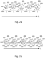
- Fig. 2 show a schematic cross-sections of LED filaments 101 according to an embodiment of the present invention.
- Fig. 2a shows cross-sections of a LED filament 101 as function of the length L of the LED filament 101.
- the cross-sections show a carrier 1005 and a plurality of LEDs 103 arranged on the carrier 1005.
- the plurality of LEDs 103 and carrier 1005, e.g., substrate are covered by an encapsulant 104.
- the encapsulant 104 comprises light scattering material 105. As depicted in Fig.
- the thickness T L of the encapsulant 104, along the LED filament length L increases over at least two adjacent first LEDs 106 and decreases over at least two adjacent second LEDs 107 different from the at least two adjacent first LEDs 106.
- the thickness T L firstly increases and secondly decreases at least along a portion of the LED filament length L. In case the encapsulant 104 is fully enclosing the LED filament it also has the reference 104.
- Fig. 2b shows cross-sections of a LED filament 101 as function of the length L of the LED filament 101.
- the cross-sections show a carrier 1005 and a plurality of LEDs 103 arranged on the carrier 1005.
- the plurality of LEDs 103 and carrier 1005, e.g. substrate, are covered by an encapsulant 104.
- the encapsulant 104 comprises light scattering material 105.
- the concentration C L of the light scattering material 105 in the encapsulant 104, along the LED filament length L increases over at least two adjacent first LEDs 106 and decreases over at least two adjacent second LEDs 107 different from the at least two adjacent first LEDs 106.
- the concentration C L firstly increases and secondly decreases at least along a portion of the LED filament length L.
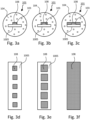
- Fig. 3a-c show a schematic cross-sections of LED filaments according to an embodiment of the present invention.
- Fig. 3d-f show a schematic top-views of carriers 1005 comprising an array 102 of a plurality of LEDs 103 according to an embodiment of the present invention.
- the LED filament 101 comprises a luminescent converter 108.
- the luminescent converter 108 at least partly covering the array 102 of the plurality of LEDs 103.
- the luminescent converter 108 is arranged between the encapsulant 104 and the array 102 of the plurality of LEDs 103.
- the luminescent converter 108 is configured to at least partly (i.e. partly or fully) convert LED light 103' into converted light 108'.
- the luminescent converter 108 may only cover the light exit of the plurality of LEDs 103 ( Fig. 3a and d ), or may only cover the light exit and sides of the plurality of LEDs 103 ( Fig. 3b and 3e ).
- the luminescent converter 108 may be provided as a continuous layer over the array 102 of the plurality of LEDs 103 (and the surface of the carrier 1005).
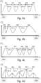
- Fig. 4a-d show schematic concentration and/or thickness profiles (as function of the LED filament length L) according to an embodiment of the present invention.
- the LED filament 101 may comprise a plurality of subsequent increases and decreases in thickness T L of the encapsulant 104 and/or concentration C L of the light scattering material 105 in the encapsulant 104 forming a plurality of M maxima in said thicknesses T L and/or said concentrations C L along the LED filament length L.
- the distance D between said maxima M may be varied along the LED filament length (L) e.g. increase (see e.g. D1-2, D2-3, D3-4).
- the LED filament may have at least four maxima M and at least three different distances between said maxima.
- the distance D between said maxima M may be randomly varied along the LED filament length L (see e.g. D1-2, D2-3, D3-4, D4-5).
- said maxima M may have different thicknesses T L of the encapsulant 104 and/or concentrations C L of the light scattering material 105 in the encapsulant 104 along the LED filament length L (see M1, M2, M3, M4, M5).
- the LED filament may have at least three maxima M which have different thicknesses T L of the encapsulant 104 and/or concentrations C L of the light scattering material 105 in the encapsulant 104 along the LED filament length L.
- the number of said maxima M is at least 5 such as 5 (see M1, M2, M3, M4, M5).
- the thickness T L of the encapsulant 104 and/or concentration C L of the light scattering material 105 in the encapsulant 104 of at least three maxima M are different (see M1, M2, M3, M4, M5).
- At least one of the thickness T L of the encapsulant 104 and the concentration C L of the light scattering material 105 in the encapsulant 104 increases and/or decreases non-linearly.
- Fig. 5 shows a side-view two LED filaments 101 according to an embodiment of the present invention.
- the at least one LED filament 101 comprises a first LED filament 101A and a second LED filament 101B.
- the at least one LED filament 101 comprises three, four, five, six, seven, eight, nine, ten, eleven or twelve LED filaments 101.
- the first LED filament 101A and the second LED filament 101B are mutually different in thickness T L and/or concentration C L profile.
- the LED filament lamp 100 further comprising a control unit 400 coupled to the first LED filament 101A and the second LED filament 101B and is configured to individually control the current supply to the first LED filament 101A and the second LED filament 101B.
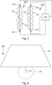
- a luminaire 200 comprises a reflector 201 and the LED filament lamp 100, wherein the LED filament lamp 100 is at least partly arranged inside the reflector 201.
- the LED filament lamp 100 may be configured to provide white light.
- the LED filament 101 may be configured to provide white light.
- white light herein, is known to the person skilled in the art and relates to white light having a correlated color temperature (CCT) between about 2000 K and 20000 K.
- CCT correlated color temperature
- the CCT is between 2100 K and 6000K.
- the CCT is in the range of about 2200K to 6500K.
- it relates to white light having a color point within about 15, 10 or 5 SDCM (standard deviation of color matching) from the BBL (black body locus).
- it relates to white light having a color rendering index (CRI) of at least 70 to 75, for general lighting at least 80 to 85.
- CRI color rendering index
- substantially herein, such as in “substantially all light” or in “substantially consists”, will be understood by the person skilled in the art.
- the term “substantially” may also include embodiments with “entirely”, “completely”, “all”, etc. Hence, in embodiments the adjective substantially may also be removed.
- the term “substantially” may also relate to 90% or higher, such as 95% or higher, especially 99% or higher, even more especially 99.5% or higher, including 100%.
- the term “comprise” includes also embodiments wherein the term “comprises” means “consists of'.
- the term “and/or” especially relates to one or more of the items mentioned before and after "and/or”.
- a phrase “item 1 and/or item 2" and similar phrases may relate to one or more of item 1 and item 2.
- the term “comprising” may in an embodiment refer to “consisting of” but may in another embodiment also refer to "containing at least the defined species and optionally one or more other species”.
- the invention further applies to a device comprising one or more of the characterizing features described in the description and/or shown in the attached drawings.
Landscapes
- Engineering & Computer Science (AREA)
- Physics & Mathematics (AREA)
- Microelectronics & Electronic Packaging (AREA)
- Optics & Photonics (AREA)
- General Engineering & Computer Science (AREA)
- Non-Portable Lighting Devices Or Systems Thereof (AREA)
Claims (13)
- Filament-Lampe mit lichtemittierenden Dioden, LED-Filament-Lampe, (100), die LED-Filament-Lampen-Licht (100') bereitstellt und mindestens ein LED-Filament (101) umfasst, das eine LED-Filament-Länge (L) aufweist, die sich von einem ersten Ende (1003) zu einem zweiten Ende (1004) erstreckt, wobei das mindestens eine LED-Filament (101) ein LED-Filament-Licht (101') bereitstellt und umfasst:- eine Anordnung (102) einer Vielzahl von LEDs (103), die ein LED-Licht (103') bereitstellen und sich entlang der LED-Filament-Länge (L) erstrecken, und- ein Verkapselungsmittel (104), das die Vielzahl von LEDs (103) mindestens teilweise umschließt, wobei das Verkapselungsmittel (104) ein lichtstreuendes Material (105) umfasst; und- wobei in der Richtung von dem ersten Ende (1003) zu dem zweiten Ende (1004) mindestens eines von(i) der Dicke (TL) des Verkapselungsmittels (104) und(ii) der Konzentration (CL) des lichtstreuenden Materials (105) in dem Verkapselungsmittel (104) entlang der LED-Filament-Länge (L) über mindestens zwei benachbarte erste LEDs (106) zunimmt und über mindestens zwei benachbarte zweite LEDs (107), die sich von den mindestens zwei benachbarten ersten LEDs (106) unterscheiden, abnimmt, und- wobei die Dicke (TL) und/oder die Konzentration (CL) mindestens entlang eines Abschnitts der LED-Filament-Länge (L) zunächst zunimmt und dann abnimmt,- wobei das LED-Filament (101) eine Vielzahl von aufeinanderfolgenden Zunahmen und Abnahmen der Dicke (TL) des Verkapselungsmittels (104) und/oder der Konzentration (CL) des lichtstreuenden Materials (105) in dem Verkapselungsmittel (104) umfasst, die eine Vielzahl von (M)-Maxima in den Dicken (TL) und/oder den Konzentrationen (CL) entlang der LED-Filament-Länge (L) bilden, und- wobei die Dicke (TL) des Verkapselungsmittels (104) und/oder die Konzentration (CL) des lichtstreuenden Materials (105) in dem Verkapselungsmittel (104) von mindestens drei Maxima (M) unterschiedlich sind;- wobei die Zunahme und/oder Abnahme der Dicke (TL) des Verkapselungsmittels (104) und/oder der Konzentration (CL) des lichtstreuenden Materials (105) in dem Verkapselungsmittel (104) allmählich ist;- wobei mindestens eines von der Dicke (TL) des Verkapselungsmittels (104) und der Konzentration (CL) des lichtstreuenden Materials (105) in dem Verkapselungsmittel (104) nichtlinear zunimmt und/oder abnimmt;- wobei (i) die Maxima eine Maxima-Höhe aufweisen und zwischen den Maxima Minima liegen, die eine Minima-Höhe aufweisen, wobei die Maxima-Höhe mindestens das 1,7-Fache der Minima-Höhe beträgt, und/oder (ii) die Maxima eine Maxima-Konzentration aufweisen und zwischen den Maxima Minima liegen, die eine Minima-Konzentration aufweisen, wobei die Maxima-Konzentration mindestens das 1,7-Fache der Minima-Konzentration beträgt.
- LED-Filament-Lampe (100) nach einem der vorstehenden Ansprüche, wobei das LED-Filament (101) einen Lumineszenzkonverter (108) umfasst, wobei der Lumineszenzkonverter (108) die Anordnung (102) der Vielzahl von LEDs (103) mindestens teilweise bedeckt, wobei der Lumineszenzkonverter (108) zwischen dem Verkapselungsmittel (104) und der Anordnung (102) der Vielzahl von LEDs angeordnet ist, wobei der Lumineszenzkonverter (108) so konfiguriert ist, dass er das LED-Licht (103') mindestens teilweise in konvertiertes Licht (108') konvertiert.
- LED-Filament-Lampe (100) nach Anspruch 2, wobei der Lumineszenzkonverter (108) als kontinuierliche Schicht über die Anordnung (102) der Vielzahl von LEDs (103) bereitgestellt ist.
- LED-Filament-Lampe (100) nach einem der vorstehenden Ansprüche, wobei das lichtstreuende Material (105) kein Licht konvertiert.
- LED-Filament-Lampe (100) nach einem der vorstehenden Ansprüche, wobei die Entfernung (D) zwischen den Maxima (M) entlang der LED-Filament-Länge (L) variiert.
- LED-Filament-Lampe (100) nach Anspruch 5, wobei die Entfernung (D) zwischen den Maxima (M) entlang der LED-Filament-Länge (L) zufällig variiert.
- LED-Filament-Lampe (100) nach einem der vorstehenden Ansprüche, wobei die Maxima (M) unterschiedliche Dicken (TL) des Verkapselungsmittels (104) und/oder Konzentrationen (CL) des lichtstreuenden Materials (105) in dem Verkapselungsmittel (104) entlang der LED-Filament-Länge (L) aufweisen.
- LED-Filament-Lampe (100) nach einem der vorstehenden Ansprüche, wobei die Anzahl der Maxima (M) mindestens 5 beträgt.
- LED-Filament-Lampe (100) nach einem der vorstehenden Ansprüche, wobei die Entfernung (D) zwischen den Maxima (M) entlang der LED-Filament-Länge (L) variiert und wobei die Maxima (M) unterschiedliche Dicken (TL) des Verkapselungsmittels (104) und/oder Konzentrationen (CL) des lichtstreuenden Materials (105) in dem Verkapselungsmittel (104) entlang der LED-Filament-Länge (L) aufweisen.
- LED-Filament-Lampe (100) nach einem der vorstehenden Ansprüche, wobei das mindestens eine LED-Filament (101) ein erstes LED-Filament (101A) und ein zweites LED-Filament (101B) umfasst.
- LED-Filament-Lampe (100) nach Anspruch 10, wobei sich das erste LED-Filament (101A) und das zweite LED-Filament (101B) hinsichtlich des Profils der Dicke (TL) und/oder der Konzentration (CL) voneinander unterscheiden.
- LED-Filament-Lampe (100) nach einem der Ansprüche 10 bis 11, ferner umfassend eine Steuereinheit (400), die mit dem ersten LED-Filament (101A) und dem zweiten LED-Filament (101B) gekoppelt und so konfiguriert ist, dass sie die Stromzufuhr zu dem ersten LED-Filament (101A) und dem zweiten LED-Filament (101B) individuell steuert.
- Leuchte (200), umfassend einen Reflektor (201) und die LED-Filament-Lampe (100) nach einem der vorstehenden Ansprüche, wobei die LED-Filament-Lampe (100) mindestens teilweise innerhalb des Reflektors (201) angeordnet ist.
Applications Claiming Priority (2)
| Application Number | Priority Date | Filing Date | Title |
|---|---|---|---|
| EP19197924 | 2019-09-18 | ||
| PCT/EP2020/075526 WO2021052887A1 (en) | 2019-09-18 | 2020-09-11 | Led filament lamp |
Publications (3)
| Publication Number | Publication Date |
|---|---|
| EP4031802A1 EP4031802A1 (de) | 2022-07-27 |
| EP4031802B1 true EP4031802B1 (de) | 2024-03-20 |
| EP4031802C0 EP4031802C0 (de) | 2024-03-20 |
Family
ID=67997989
Family Applications (1)
| Application Number | Title | Priority Date | Filing Date |
|---|---|---|---|
| EP20771297.7A Active EP4031802B1 (de) | 2019-09-18 | 2020-09-11 | Led filament lampe |
Country Status (5)
| Country | Link |
|---|---|
| US (1) | US11719392B2 (de) |
| EP (1) | EP4031802B1 (de) |
| CN (1) | CN114423988B (de) |
| ES (1) | ES2980886T3 (de) |
| WO (1) | WO2021052887A1 (de) |
Families Citing this family (10)
| Publication number | Priority date | Publication date | Assignee | Title |
|---|---|---|---|---|
| US12018802B2 (en) * | 2020-06-08 | 2024-06-25 | Signify Holding B.V. | Light emitting device with sparkling effect |
| ES3041924T3 (en) * | 2021-01-06 | 2025-11-17 | Signify Holding Bv | Filament based solid state lighting device |
| US12595409B2 (en) * | 2021-06-04 | 2026-04-07 | Bridgelux, Inc. | High luminous efficacy phosphor converted white LEDs |
| US11933459B2 (en) * | 2022-04-26 | 2024-03-19 | Ledvance Llc | Lamp including reduced phosphor light emitting diode filaments |
| US12438130B2 (en) * | 2021-11-02 | 2025-10-07 | Ledvance Llc | Light emitting diode filament including chip scale package light emitting diodes to reduce the amount of phosphor that is integrated into the filament |
| WO2025082880A1 (en) | 2023-10-16 | 2025-04-24 | Signify Holding B.V. | Led filament comprising encapsulants |
| WO2025153467A1 (en) | 2024-01-16 | 2025-07-24 | Signify Holding B.V. | Light emitting diode filament arrangement |
| WO2025157677A1 (en) * | 2024-01-22 | 2025-07-31 | Signify Holding B.V. | Light emitting device |
| WO2025252440A1 (en) | 2024-06-06 | 2025-12-11 | Signify Holding B.V. | Led filament comprising encapsulants |
| WO2026077797A1 (en) * | 2024-10-10 | 2026-04-16 | Signify Holding B.V. | A flexible led strip filament |
Family Cites Families (20)
| Publication number | Priority date | Publication date | Assignee | Title |
|---|---|---|---|---|
| JP4389524B2 (ja) * | 2003-08-29 | 2009-12-24 | 日亜化学工業株式会社 | 擬似炎型発光装置及びその製造方法並びに電子炎灯 |
| US10655792B2 (en) * | 2014-09-28 | 2020-05-19 | Zhejiang Super Lighting Electric Appliance Co., Ltd. | LED bulb lamp |
| KR20130019389A (ko) * | 2010-03-03 | 2013-02-26 | 크리 인코포레이티드 | 솔리드 스테이트 램프 및 전구 |
| SG188483A1 (en) * | 2010-09-08 | 2013-04-30 | Zhejiang Ledison Optoelectronics Co Ltd | Led light bulb and led light-emitting strip being capable of emitting 4pi light |
| CN102537754A (zh) | 2010-12-14 | 2012-07-04 | 上海蓝光科技有限公司 | 侧光式背光源模组 |
| CN102147095A (zh) * | 2011-04-19 | 2011-08-10 | 广东亚一照明科技有限公司 | 一种led蜡烛灯 |
| CN103322525B (zh) * | 2013-06-17 | 2015-04-22 | 深圳市源磊科技有限公司 | Led灯及其灯丝 |
| CN103471034A (zh) * | 2013-09-03 | 2013-12-25 | 苏州市银河照明器材有限公司 | 道路照明用led仿古宫灯用光反射器 |
| CN203628400U (zh) | 2013-09-24 | 2014-06-04 | 王志根 | 一种全角度发光灯丝 |
| US11028970B2 (en) * | 2014-09-28 | 2021-06-08 | Zhejiang Super Lighting Electric Appliance Co., Ltd | LED filament light bulb having organosilicon-modified polyimide resin composition filament base layer |
| CN104879660A (zh) * | 2015-05-14 | 2015-09-02 | 西安和合光电科技有限公司 | 一种密封充气led灯 |
| WO2017157719A1 (en) | 2016-03-16 | 2017-09-21 | Lumileds Holding B.V. | Method of manufacturing an led module |
| DE102016105211A1 (de) | 2016-03-21 | 2017-09-21 | Osram Opto Semiconductors Gmbh | Filament und dessen Herstellung sowie Leuchtmittel mit Filamenten |
| DE102016105537A1 (de) | 2016-03-24 | 2017-09-28 | Osram Opto Semiconductors Gmbh | Filament mit lichtemittierenden halbleiterchips, leuchtmittel und verfahren zur herstellung eines filaments |
| JP2017191875A (ja) * | 2016-04-14 | 2017-10-19 | 株式会社小糸製作所 | 発光モジュール |
| KR20170131910A (ko) * | 2016-05-23 | 2017-12-01 | 주식회사 루멘스 | 발광소자 및 이를 포함하는 발광벌브 |
| CN107314258B (zh) | 2016-04-27 | 2020-04-10 | 嘉兴山蒲照明电器有限公司 | Led球泡灯 |
| DE102016115533A1 (de) | 2016-08-22 | 2018-02-22 | Osram Opto Semiconductors Gmbh | Optoelektronischer Halbleiterchip, Verfahren zur Herstellung eines optoelektronischen Halbleiterchips und Scheinwerfer mit einem optoelektronischen Halbleiterchip |
| CN111615753B (zh) * | 2017-12-17 | 2024-05-31 | 英特曼帝克司公司 | 可调光固态光发射装置 |
| CN109973833B (zh) | 2017-12-26 | 2023-03-28 | 嘉兴山蒲照明电器有限公司 | Led灯丝及led球泡灯 |
-
2020
- 2020-09-11 EP EP20771297.7A patent/EP4031802B1/de active Active
- 2020-09-11 CN CN202080065468.2A patent/CN114423988B/zh active Active
- 2020-09-11 WO PCT/EP2020/075526 patent/WO2021052887A1/en not_active Ceased
- 2020-09-11 US US17/761,098 patent/US11719392B2/en active Active
- 2020-09-11 ES ES20771297T patent/ES2980886T3/es active Active
Also Published As
| Publication number | Publication date |
|---|---|
| CN114423988B (zh) | 2024-03-29 |
| WO2021052887A1 (en) | 2021-03-25 |
| ES2980886T3 (es) | 2024-10-03 |
| EP4031802A1 (de) | 2022-07-27 |
| US11719392B2 (en) | 2023-08-08 |
| US20220349530A1 (en) | 2022-11-03 |
| CN114423988A (zh) | 2022-04-29 |
| EP4031802C0 (de) | 2024-03-20 |
Similar Documents
| Publication | Publication Date | Title |
|---|---|---|
| EP4031802B1 (de) | Led filament lampe | |
| US12111021B2 (en) | LED filament and LED filament lamp | |
| EP3775674B1 (de) | Led-glühlampe in kerzenlichtoptik | |
| JP7080253B2 (ja) | 照明デバイス及び照明器具 | |
| US12085238B2 (en) | LED filament | |
| CN113330245A (zh) | Led灯丝装置 | |
| EP4004432B1 (de) | Led-filament-anordnung | |
| EP4538588B1 (de) | Led-filament-anordnung | |
| US20240003505A1 (en) | Led filament | |
| CN114630986B (zh) | Led灯丝装置 | |
| WO2026017508A1 (en) | A led filament | |
| WO2025201945A1 (en) | A led filament | |
| WO2025228869A1 (en) | Led filament arrangement comprising a mixing chamber |
Legal Events
| Date | Code | Title | Description |
|---|---|---|---|
| STAA | Information on the status of an ep patent application or granted ep patent |
Free format text: STATUS: UNKNOWN |
|
| STAA | Information on the status of an ep patent application or granted ep patent |
Free format text: STATUS: THE INTERNATIONAL PUBLICATION HAS BEEN MADE |
|
| PUAI | Public reference made under article 153(3) epc to a published international application that has entered the european phase |
Free format text: ORIGINAL CODE: 0009012 |
|
| STAA | Information on the status of an ep patent application or granted ep patent |
Free format text: STATUS: REQUEST FOR EXAMINATION WAS MADE |
|
| 17P | Request for examination filed |
Effective date: 20220419 |
|
| AK | Designated contracting states |
Kind code of ref document: A1 Designated state(s): AL AT BE BG CH CY CZ DE DK EE ES FI FR GB GR HR HU IE IS IT LI LT LU LV MC MK MT NL NO PL PT RO RS SE SI SK SM TR |
|
| DAV | Request for validation of the european patent (deleted) | ||
| DAX | Request for extension of the european patent (deleted) | ||
| GRAP | Despatch of communication of intention to grant a patent |
Free format text: ORIGINAL CODE: EPIDOSNIGR1 |
|
| STAA | Information on the status of an ep patent application or granted ep patent |
Free format text: STATUS: GRANT OF PATENT IS INTENDED |
|
| INTG | Intention to grant announced |
Effective date: 20231016 |
|
| GRAS | Grant fee paid |
Free format text: ORIGINAL CODE: EPIDOSNIGR3 |
|
| GRAA | (expected) grant |
Free format text: ORIGINAL CODE: 0009210 |
|
| STAA | Information on the status of an ep patent application or granted ep patent |
Free format text: STATUS: THE PATENT HAS BEEN GRANTED |
|
| AK | Designated contracting states |
Kind code of ref document: B1 Designated state(s): AL AT BE BG CH CY CZ DE DK EE ES FI FR GB GR HR HU IE IS IT LI LT LU LV MC MK MT NL NO PL PT RO RS SE SI SK SM TR |
|
| REG | Reference to a national code |
Ref country code: GB Ref legal event code: FG4D |
|
| REG | Reference to a national code |
Ref country code: CH Ref legal event code: EP |
|
| REG | Reference to a national code |
Ref country code: DE Ref legal event code: R096 Ref document number: 602020027577 Country of ref document: DE |
|
| REG | Reference to a national code |
Ref country code: IE Ref legal event code: FG4D |
|
| U01 | Request for unitary effect filed |
Effective date: 20240412 |
|
| U07 | Unitary effect registered |
Designated state(s): AT BE BG DE DK EE FI FR IT LT LU LV MT NL PT SE SI Effective date: 20240419 |
|
| PG25 | Lapsed in a contracting state [announced via postgrant information from national office to epo] |
Ref country code: GR Free format text: LAPSE BECAUSE OF FAILURE TO SUBMIT A TRANSLATION OF THE DESCRIPTION OR TO PAY THE FEE WITHIN THE PRESCRIBED TIME-LIMIT Effective date: 20240621 |
|
| PG25 | Lapsed in a contracting state [announced via postgrant information from national office to epo] |
Ref country code: HR Free format text: LAPSE BECAUSE OF FAILURE TO SUBMIT A TRANSLATION OF THE DESCRIPTION OR TO PAY THE FEE WITHIN THE PRESCRIBED TIME-LIMIT Effective date: 20240320 Ref country code: RS Free format text: LAPSE BECAUSE OF FAILURE TO SUBMIT A TRANSLATION OF THE DESCRIPTION OR TO PAY THE FEE WITHIN THE PRESCRIBED TIME-LIMIT Effective date: 20240620 |
|
| PG25 | Lapsed in a contracting state [announced via postgrant information from national office to epo] |
Ref country code: RS Free format text: LAPSE BECAUSE OF FAILURE TO SUBMIT A TRANSLATION OF THE DESCRIPTION OR TO PAY THE FEE WITHIN THE PRESCRIBED TIME-LIMIT Effective date: 20240620 Ref country code: NO Free format text: LAPSE BECAUSE OF FAILURE TO SUBMIT A TRANSLATION OF THE DESCRIPTION OR TO PAY THE FEE WITHIN THE PRESCRIBED TIME-LIMIT Effective date: 20240620 Ref country code: HR Free format text: LAPSE BECAUSE OF FAILURE TO SUBMIT A TRANSLATION OF THE DESCRIPTION OR TO PAY THE FEE WITHIN THE PRESCRIBED TIME-LIMIT Effective date: 20240320 Ref country code: GR Free format text: LAPSE BECAUSE OF FAILURE TO SUBMIT A TRANSLATION OF THE DESCRIPTION OR TO PAY THE FEE WITHIN THE PRESCRIBED TIME-LIMIT Effective date: 20240621 |
|
| REG | Reference to a national code |
Ref country code: ES Ref legal event code: FG2A Ref document number: 2980886 Country of ref document: ES Kind code of ref document: T3 Effective date: 20241003 |
|
| PG25 | Lapsed in a contracting state [announced via postgrant information from national office to epo] |
Ref country code: IS Free format text: LAPSE BECAUSE OF FAILURE TO SUBMIT A TRANSLATION OF THE DESCRIPTION OR TO PAY THE FEE WITHIN THE PRESCRIBED TIME-LIMIT Effective date: 20240720 |
|
| PG25 | Lapsed in a contracting state [announced via postgrant information from national office to epo] |
Ref country code: SM Free format text: LAPSE BECAUSE OF FAILURE TO SUBMIT A TRANSLATION OF THE DESCRIPTION OR TO PAY THE FEE WITHIN THE PRESCRIBED TIME-LIMIT Effective date: 20240320 |
|
| PG25 | Lapsed in a contracting state [announced via postgrant information from national office to epo] |
Ref country code: CZ Free format text: LAPSE BECAUSE OF FAILURE TO SUBMIT A TRANSLATION OF THE DESCRIPTION OR TO PAY THE FEE WITHIN THE PRESCRIBED TIME-LIMIT Effective date: 20240320 |
|
| PG25 | Lapsed in a contracting state [announced via postgrant information from national office to epo] |
Ref country code: PL Free format text: LAPSE BECAUSE OF FAILURE TO SUBMIT A TRANSLATION OF THE DESCRIPTION OR TO PAY THE FEE WITHIN THE PRESCRIBED TIME-LIMIT Effective date: 20240320 |
|
| PG25 | Lapsed in a contracting state [announced via postgrant information from national office to epo] |
Ref country code: SK Free format text: LAPSE BECAUSE OF FAILURE TO SUBMIT A TRANSLATION OF THE DESCRIPTION OR TO PAY THE FEE WITHIN THE PRESCRIBED TIME-LIMIT Effective date: 20240320 |
|
| U20 | Renewal fee for the european patent with unitary effect paid |
Year of fee payment: 5 Effective date: 20240926 |
|
| PG25 | Lapsed in a contracting state [announced via postgrant information from national office to epo] |
Ref country code: SM Free format text: LAPSE BECAUSE OF FAILURE TO SUBMIT A TRANSLATION OF THE DESCRIPTION OR TO PAY THE FEE WITHIN THE PRESCRIBED TIME-LIMIT Effective date: 20240320 Ref country code: SK Free format text: LAPSE BECAUSE OF FAILURE TO SUBMIT A TRANSLATION OF THE DESCRIPTION OR TO PAY THE FEE WITHIN THE PRESCRIBED TIME-LIMIT Effective date: 20240320 Ref country code: RO Free format text: LAPSE BECAUSE OF FAILURE TO SUBMIT A TRANSLATION OF THE DESCRIPTION OR TO PAY THE FEE WITHIN THE PRESCRIBED TIME-LIMIT Effective date: 20240320 Ref country code: PL Free format text: LAPSE BECAUSE OF FAILURE TO SUBMIT A TRANSLATION OF THE DESCRIPTION OR TO PAY THE FEE WITHIN THE PRESCRIBED TIME-LIMIT Effective date: 20240320 Ref country code: IS Free format text: LAPSE BECAUSE OF FAILURE TO SUBMIT A TRANSLATION OF THE DESCRIPTION OR TO PAY THE FEE WITHIN THE PRESCRIBED TIME-LIMIT Effective date: 20240720 Ref country code: CZ Free format text: LAPSE BECAUSE OF FAILURE TO SUBMIT A TRANSLATION OF THE DESCRIPTION OR TO PAY THE FEE WITHIN THE PRESCRIBED TIME-LIMIT Effective date: 20240320 |
|
| REG | Reference to a national code |
Ref country code: DE Ref legal event code: R097 Ref document number: 602020027577 Country of ref document: DE |
|
| PLBE | No opposition filed within time limit |
Free format text: ORIGINAL CODE: 0009261 |
|
| STAA | Information on the status of an ep patent application or granted ep patent |
Free format text: STATUS: NO OPPOSITION FILED WITHIN TIME LIMIT |
|
| 26N | No opposition filed |
Effective date: 20241223 |
|
| PG25 | Lapsed in a contracting state [announced via postgrant information from national office to epo] |
Ref country code: MC Free format text: LAPSE BECAUSE OF FAILURE TO SUBMIT A TRANSLATION OF THE DESCRIPTION OR TO PAY THE FEE WITHIN THE PRESCRIBED TIME-LIMIT Effective date: 20240320 |
|
| REG | Reference to a national code |
Ref country code: CH Ref legal event code: PL |
|
| PG25 | Lapsed in a contracting state [announced via postgrant information from national office to epo] |
Ref country code: CH Free format text: LAPSE BECAUSE OF NON-PAYMENT OF DUE FEES Effective date: 20240930 |
|
| PG25 | Lapsed in a contracting state [announced via postgrant information from national office to epo] |
Ref country code: IE Free format text: LAPSE BECAUSE OF NON-PAYMENT OF DUE FEES Effective date: 20240911 |
|
| PGFP | Annual fee paid to national office [announced via postgrant information from national office to epo] |
Ref country code: GB Payment date: 20250923 Year of fee payment: 6 |
|
| REG | Reference to a national code |
Ref country code: ES Ref legal event code: FD2A Effective date: 20251024 |
|
| U20 | Renewal fee for the european patent with unitary effect paid |
Year of fee payment: 6 Effective date: 20250925 |
|
| PG25 | Lapsed in a contracting state [announced via postgrant information from national office to epo] |
Ref country code: CY Free format text: LAPSE BECAUSE OF FAILURE TO SUBMIT A TRANSLATION OF THE DESCRIPTION OR TO PAY THE FEE WITHIN THE PRESCRIBED TIME-LIMIT; INVALID AB INITIO Effective date: 20200911 |
|
| PG25 | Lapsed in a contracting state [announced via postgrant information from national office to epo] |
Ref country code: ES Free format text: LAPSE BECAUSE OF NON-PAYMENT OF DUE FEES Effective date: 20240912 |
|
| PG25 | Lapsed in a contracting state [announced via postgrant information from national office to epo] |
Ref country code: HU Free format text: LAPSE BECAUSE OF FAILURE TO SUBMIT A TRANSLATION OF THE DESCRIPTION OR TO PAY THE FEE WITHIN THE PRESCRIBED TIME-LIMIT; INVALID AB INITIO Effective date: 20200911 |