EP4027373A1 - Source/drain electrode for organic semiconductor device, organic semiconductor device using same, and production method for source/drain electrode and semiconductor device - Google Patents
Source/drain electrode for organic semiconductor device, organic semiconductor device using same, and production method for source/drain electrode and semiconductor device Download PDFInfo
- Publication number
- EP4027373A1 EP4027373A1 EP20861639.1A EP20861639A EP4027373A1 EP 4027373 A1 EP4027373 A1 EP 4027373A1 EP 20861639 A EP20861639 A EP 20861639A EP 4027373 A1 EP4027373 A1 EP 4027373A1
- Authority
- EP
- European Patent Office
- Prior art keywords
- electrodes
- film
- organic semiconductor
- substrate
- drain
- Prior art date
- Legal status (The legal status is an assumption and is not a legal conclusion. Google has not performed a legal analysis and makes no representation as to the accuracy of the status listed.)
- Pending
Links
- 239000004065 semiconductor Substances 0.000 title claims abstract description 247
- 238000004519 manufacturing process Methods 0.000 title claims abstract description 23
- 230000003746 surface roughness Effects 0.000 claims abstract description 46
- 239000000758 substrate Substances 0.000 claims description 152
- 230000001681 protective effect Effects 0.000 claims description 144
- 238000000034 method Methods 0.000 claims description 111
- 229920000642 polymer Polymers 0.000 claims description 74
- 239000005871 repellent Substances 0.000 claims description 60
- 238000007747 plating Methods 0.000 claims description 56
- 125000002887 hydroxy group Chemical group [H]O* 0.000 claims description 48
- 239000002923 metal particle Substances 0.000 claims description 19
- 229910052751 metal Inorganic materials 0.000 claims description 18
- 239000002184 metal Substances 0.000 claims description 18
- 230000009477 glass transition Effects 0.000 claims description 17
- 238000007772 electroless plating Methods 0.000 claims description 12
- CBENFWSGALASAD-UHFFFAOYSA-N Ozone Chemical compound [O-][O+]=O CBENFWSGALASAD-UHFFFAOYSA-N 0.000 claims description 9
- 239000003054 catalyst Substances 0.000 claims description 9
- 238000009281 ultraviolet germicidal irradiation Methods 0.000 claims description 9
- 230000008859 change Effects 0.000 abstract description 8
- 239000010408 film Substances 0.000 description 490
- 239000010410 layer Substances 0.000 description 152
- 239000013545 self-assembled monolayer Substances 0.000 description 90
- 239000002094 self assembled monolayer Substances 0.000 description 67
- 239000010931 gold Substances 0.000 description 60
- 125000000217 alkyl group Chemical group 0.000 description 40
- 238000000576 coating method Methods 0.000 description 37
- 239000004372 Polyvinyl alcohol Substances 0.000 description 35
- 229920002451 polyvinyl alcohol Polymers 0.000 description 35
- 238000012546 transfer Methods 0.000 description 33
- 239000011521 glass Substances 0.000 description 29
- 239000013078 crystal Substances 0.000 description 25
- 239000007924 injection Substances 0.000 description 25
- 238000002347 injection Methods 0.000 description 25
- 229920003229 poly(methyl methacrylate) Polymers 0.000 description 25
- 239000004926 polymethyl methacrylate Substances 0.000 description 25
- XLYOFNOQVPJJNP-UHFFFAOYSA-N water Substances O XLYOFNOQVPJJNP-UHFFFAOYSA-N 0.000 description 25
- 239000011248 coating agent Substances 0.000 description 24
- 239000002904 solvent Substances 0.000 description 24
- 125000004435 hydrogen atom Chemical group [H]* 0.000 description 23
- 229920000052 poly(p-xylylene) Polymers 0.000 description 23
- 239000000243 solution Substances 0.000 description 22
- VYPSYNLAJGMNEJ-UHFFFAOYSA-N Silicium dioxide Chemical compound O=[Si]=O VYPSYNLAJGMNEJ-UHFFFAOYSA-N 0.000 description 20
- 125000004432 carbon atom Chemical group C* 0.000 description 20
- 229920006395 saturated elastomer Polymers 0.000 description 17
- 239000002245 particle Substances 0.000 description 16
- 230000001737 promoting effect Effects 0.000 description 16
- KFZMGEQAYNKOFK-UHFFFAOYSA-N Isopropanol Chemical compound CC(C)O KFZMGEQAYNKOFK-UHFFFAOYSA-N 0.000 description 15
- 239000000463 material Substances 0.000 description 14
- 229920003169 water-soluble polymer Polymers 0.000 description 14
- TVMXDCGIABBOFY-UHFFFAOYSA-N octane Chemical compound CCCCCCCC TVMXDCGIABBOFY-UHFFFAOYSA-N 0.000 description 13
- YXFVVABEGXRONW-UHFFFAOYSA-N Toluene Chemical compound CC1=CC=CC=C1 YXFVVABEGXRONW-UHFFFAOYSA-N 0.000 description 12
- KQAHMVLQCSALSX-UHFFFAOYSA-N decyl(trimethoxy)silane Chemical compound CCCCCCCCCC[Si](OC)(OC)OC KQAHMVLQCSALSX-UHFFFAOYSA-N 0.000 description 12
- 238000005259 measurement Methods 0.000 description 12
- 238000004220 aggregation Methods 0.000 description 11
- 238000010438 heat treatment Methods 0.000 description 11
- 238000004630 atomic force microscopy Methods 0.000 description 10
- 229910052681 coesite Inorganic materials 0.000 description 10
- 229910052906 cristobalite Inorganic materials 0.000 description 10
- 230000005669 field effect Effects 0.000 description 10
- 239000002052 molecular layer Substances 0.000 description 10
- -1 polydimethylsiloxane Polymers 0.000 description 10
- 239000000377 silicon dioxide Substances 0.000 description 10
- 238000004528 spin coating Methods 0.000 description 10
- 229910052682 stishovite Inorganic materials 0.000 description 10
- 229910052905 tridymite Inorganic materials 0.000 description 10
- 238000005266 casting Methods 0.000 description 9
- 238000001771 vacuum deposition Methods 0.000 description 8
- 239000012298 atmosphere Substances 0.000 description 7
- 230000006378 damage Effects 0.000 description 7
- 229920001971 elastomer Polymers 0.000 description 7
- 239000000806 elastomer Substances 0.000 description 7
- 239000003960 organic solvent Substances 0.000 description 7
- 238000000206 photolithography Methods 0.000 description 7
- 229920003223 poly(pyromellitimide-1,4-diphenyl ether) Polymers 0.000 description 7
- 229920006254 polymer film Polymers 0.000 description 7
- 230000008569 process Effects 0.000 description 7
- 239000002356 single layer Substances 0.000 description 7
- IXHWGNYCZPISET-UHFFFAOYSA-N 2-[4-(dicyanomethylidene)-2,3,5,6-tetrafluorocyclohexa-2,5-dien-1-ylidene]propanedinitrile Chemical group FC1=C(F)C(=C(C#N)C#N)C(F)=C(F)C1=C(C#N)C#N IXHWGNYCZPISET-UHFFFAOYSA-N 0.000 description 6
- WEVYAHXRMPXWCK-UHFFFAOYSA-N Acetonitrile Chemical compound CC#N WEVYAHXRMPXWCK-UHFFFAOYSA-N 0.000 description 6
- 239000004205 dimethyl polysiloxane Substances 0.000 description 6
- 235000013870 dimethyl polysiloxane Nutrition 0.000 description 6
- 239000007772 electrode material Substances 0.000 description 6
- 229910052731 fluorine Inorganic materials 0.000 description 6
- 239000011737 fluorine Substances 0.000 description 6
- 125000003709 fluoroalkyl group Chemical group 0.000 description 6
- 229910052737 gold Inorganic materials 0.000 description 6
- 229920000435 poly(dimethylsiloxane) Polymers 0.000 description 6
- UVAMFBJPMUMURT-UHFFFAOYSA-N 2,3,4,5,6-pentafluorobenzenethiol Chemical compound FC1=C(F)C(F)=C(S)C(F)=C1F UVAMFBJPMUMURT-UHFFFAOYSA-N 0.000 description 5
- WLHCBQAPPJAULW-UHFFFAOYSA-N 4-methylbenzenethiol Chemical compound CC1=CC=C(S)C=C1 WLHCBQAPPJAULW-UHFFFAOYSA-N 0.000 description 5
- YCKRFDGAMUMZLT-UHFFFAOYSA-N Fluorine atom Chemical compound [F] YCKRFDGAMUMZLT-UHFFFAOYSA-N 0.000 description 5
- 125000005842 heteroatom Chemical group 0.000 description 5
- 125000004430 oxygen atom Chemical group O* 0.000 description 5
- 238000000085 photoelectron yield spectroscopy Methods 0.000 description 5
- 239000000126 substance Substances 0.000 description 5
- 229910052717 sulfur Inorganic materials 0.000 description 5
- 125000004434 sulfur atom Chemical group 0.000 description 5
- MLXDKRSDUJLNAB-UHFFFAOYSA-N triethoxy(3,3,4,4,5,5,6,6,7,7,8,8,9,9,10,10,10-heptadecafluorodecyl)silane Chemical compound CCO[Si](OCC)(OCC)CCC(F)(F)C(F)(F)C(F)(F)C(F)(F)C(F)(F)C(F)(F)C(F)(F)C(F)(F)F MLXDKRSDUJLNAB-UHFFFAOYSA-N 0.000 description 5
- OKTJSMMVPCPJKN-UHFFFAOYSA-N Carbon Chemical compound [C] OKTJSMMVPCPJKN-UHFFFAOYSA-N 0.000 description 4
- 239000007864 aqueous solution Substances 0.000 description 4
- QVGXLLKOCUKJST-UHFFFAOYSA-N atomic oxygen Chemical compound [O] QVGXLLKOCUKJST-UHFFFAOYSA-N 0.000 description 4
- 230000005540 biological transmission Effects 0.000 description 4
- 229910052799 carbon Inorganic materials 0.000 description 4
- 238000005229 chemical vapour deposition Methods 0.000 description 4
- 238000001035 drying Methods 0.000 description 4
- 238000011156 evaluation Methods 0.000 description 4
- 125000005843 halogen group Chemical group 0.000 description 4
- 229910052760 oxygen Inorganic materials 0.000 description 4
- 239000001301 oxygen Substances 0.000 description 4
- 238000000059 patterning Methods 0.000 description 4
- 125000001997 phenyl group Chemical group [H]C1=C([H])C([H])=C(*)C([H])=C1[H] 0.000 description 4
- 238000007639 printing Methods 0.000 description 4
- 125000001424 substituent group Chemical group 0.000 description 4
- UBMUZYGBAGFCDF-UHFFFAOYSA-N trimethoxy(2-phenylethyl)silane Chemical compound CO[Si](OC)(OC)CCC1=CC=CC=C1 UBMUZYGBAGFCDF-UHFFFAOYSA-N 0.000 description 4
- 238000012935 Averaging Methods 0.000 description 3
- CERQOIWHTDAKMF-UHFFFAOYSA-M Methacrylate Chemical compound CC(=C)C([O-])=O CERQOIWHTDAKMF-UHFFFAOYSA-M 0.000 description 3
- 230000000052 comparative effect Effects 0.000 description 3
- 238000010790 dilution Methods 0.000 description 3
- 239000012895 dilution Substances 0.000 description 3
- 238000003618 dip coating Methods 0.000 description 3
- 230000000694 effects Effects 0.000 description 3
- 229910021645 metal ion Inorganic materials 0.000 description 3
- 239000000178 monomer Substances 0.000 description 3
- 229920000139 polyethylene terephthalate Polymers 0.000 description 3
- 239000005020 polyethylene terephthalate Substances 0.000 description 3
- 229920000123 polythiophene Polymers 0.000 description 3
- 229910052710 silicon Inorganic materials 0.000 description 3
- 239000010703 silicon Substances 0.000 description 3
- 229910052709 silver Inorganic materials 0.000 description 3
- 239000007787 solid Substances 0.000 description 3
- 239000010409 thin film Substances 0.000 description 3
- 239000012808 vapor phase Substances 0.000 description 3
- 238000005406 washing Methods 0.000 description 3
- DKPFZGUDAPQIHT-UHFFFAOYSA-N Butyl acetate Natural products CCCCOC(C)=O DKPFZGUDAPQIHT-UHFFFAOYSA-N 0.000 description 2
- VYZAMTAEIAYCRO-UHFFFAOYSA-N Chromium Chemical compound [Cr] VYZAMTAEIAYCRO-UHFFFAOYSA-N 0.000 description 2
- LFQSCWFLJHTTHZ-UHFFFAOYSA-N Ethanol Chemical compound CCO LFQSCWFLJHTTHZ-UHFFFAOYSA-N 0.000 description 2
- 239000004813 Perfluoroalkoxy alkane Substances 0.000 description 2
- 239000004698 Polyethylene Substances 0.000 description 2
- XUIMIQQOPSSXEZ-UHFFFAOYSA-N Silicon Chemical compound [Si] XUIMIQQOPSSXEZ-UHFFFAOYSA-N 0.000 description 2
- YTPLMLYBLZKORZ-UHFFFAOYSA-N Thiophene Chemical compound C=1C=CSC=1 YTPLMLYBLZKORZ-UHFFFAOYSA-N 0.000 description 2
- 239000000853 adhesive Substances 0.000 description 2
- 230000001070 adhesive effect Effects 0.000 description 2
- 239000000969 carrier Substances 0.000 description 2
- 229910052804 chromium Inorganic materials 0.000 description 2
- 239000011651 chromium Substances 0.000 description 2
- 229920001940 conductive polymer Polymers 0.000 description 2
- 239000000539 dimer Substances 0.000 description 2
- 230000001747 exhibiting effect Effects 0.000 description 2
- 125000001207 fluorophenyl group Chemical group 0.000 description 2
- PCHJSUWPFVWCPO-UHFFFAOYSA-N gold Chemical compound [Au] PCHJSUWPFVWCPO-UHFFFAOYSA-N 0.000 description 2
- 238000007646 gravure printing Methods 0.000 description 2
- FUZZWVXGSFPDMH-UHFFFAOYSA-N hexanoic acid Chemical compound CCCCCC(O)=O FUZZWVXGSFPDMH-UHFFFAOYSA-N 0.000 description 2
- 238000007641 inkjet printing Methods 0.000 description 2
- 239000007791 liquid phase Substances 0.000 description 2
- 230000007774 longterm Effects 0.000 description 2
- 238000007645 offset printing Methods 0.000 description 2
- 229920011301 perfluoro alkoxyl alkane Polymers 0.000 description 2
- 229920003023 plastic Polymers 0.000 description 2
- 239000004033 plastic Substances 0.000 description 2
- 229920002239 polyacrylonitrile Polymers 0.000 description 2
- 229920000573 polyethylene Polymers 0.000 description 2
- 239000011112 polyethylene naphthalate Substances 0.000 description 2
- 239000000843 powder Substances 0.000 description 2
- 238000006722 reduction reaction Methods 0.000 description 2
- 238000007650 screen-printing Methods 0.000 description 2
- 238000000926 separation method Methods 0.000 description 2
- 239000007921 spray Substances 0.000 description 2
- 238000005507 spraying Methods 0.000 description 2
- BGHCVCJVXZWKCC-UHFFFAOYSA-N tetradecane Chemical compound CCCCCCCCCCCCCC BGHCVCJVXZWKCC-UHFFFAOYSA-N 0.000 description 2
- 230000003685 thermal hair damage Effects 0.000 description 2
- QUBJDMPBDURTJT-UHFFFAOYSA-N 3-chlorothiophene Chemical compound ClC=1C=CSC=1 QUBJDMPBDURTJT-UHFFFAOYSA-N 0.000 description 1
- XDTMQSROBMDMFD-UHFFFAOYSA-N Cyclohexane Chemical compound C1CCCCC1 XDTMQSROBMDMFD-UHFFFAOYSA-N 0.000 description 1
- 229920002307 Dextran Polymers 0.000 description 1
- 229920002845 Poly(methacrylic acid) Polymers 0.000 description 1
- 239000004793 Polystyrene Substances 0.000 description 1
- 229920002125 Sokalan® Polymers 0.000 description 1
- PNEYBMLMFCGWSK-UHFFFAOYSA-N aluminium oxide Inorganic materials [O-2].[O-2].[O-2].[Al+3].[Al+3] PNEYBMLMFCGWSK-UHFFFAOYSA-N 0.000 description 1
- 229910021417 amorphous silicon Inorganic materials 0.000 description 1
- 238000006243 chemical reaction Methods 0.000 description 1
- 239000003638 chemical reducing agent Substances 0.000 description 1
- 239000008139 complexing agent Substances 0.000 description 1
- 238000007796 conventional method Methods 0.000 description 1
- 238000001816 cooling Methods 0.000 description 1
- 229910052802 copper Inorganic materials 0.000 description 1
- 238000000354 decomposition reaction Methods 0.000 description 1
- 238000000151 deposition Methods 0.000 description 1
- 230000008021 deposition Effects 0.000 description 1
- 238000010586 diagram Methods 0.000 description 1
- 238000007865 diluting Methods 0.000 description 1
- KPUWHANPEXNPJT-UHFFFAOYSA-N disiloxane Chemical class [SiH3]O[SiH3] KPUWHANPEXNPJT-UHFFFAOYSA-N 0.000 description 1
- 238000005401 electroluminescence Methods 0.000 description 1
- 238000009713 electroplating Methods 0.000 description 1
- 230000002349 favourable effect Effects 0.000 description 1
- 125000001153 fluoro group Chemical group F* 0.000 description 1
- 150000002391 heterocyclic compounds Chemical class 0.000 description 1
- 125000004051 hexyl group Chemical group [H]C([H])([H])C([H])([H])C([H])([H])C([H])([H])C([H])([H])C([H])([H])* 0.000 description 1
- 238000004770 highest occupied molecular orbital Methods 0.000 description 1
- 230000002209 hydrophobic effect Effects 0.000 description 1
- 239000011229 interlayer Substances 0.000 description 1
- 230000001678 irradiating effect Effects 0.000 description 1
- 229910052759 nickel Inorganic materials 0.000 description 1
- 229910052763 palladium Inorganic materials 0.000 description 1
- NRNCYVBFPDDJNE-UHFFFAOYSA-N pemoline Chemical compound O1C(N)=NC(=O)C1C1=CC=CC=C1 NRNCYVBFPDDJNE-UHFFFAOYSA-N 0.000 description 1
- 230000000704 physical effect Effects 0.000 description 1
- 229910052697 platinum Inorganic materials 0.000 description 1
- 238000005498 polishing Methods 0.000 description 1
- 229920003207 poly(ethylene-2,6-naphthalate) Polymers 0.000 description 1
- 239000004584 polyacrylic acid Substances 0.000 description 1
- 229910021420 polycrystalline silicon Inorganic materials 0.000 description 1
- 239000002244 precipitate Substances 0.000 description 1
- 238000012545 processing Methods 0.000 description 1
- 238000010526 radical polymerization reaction Methods 0.000 description 1
- 230000009467 reduction Effects 0.000 description 1
- 230000001373 regressive effect Effects 0.000 description 1
- 238000001878 scanning electron micrograph Methods 0.000 description 1
- 239000004332 silver Substances 0.000 description 1
- 238000004467 single crystal X-ray diffraction Methods 0.000 description 1
- 230000000087 stabilizing effect Effects 0.000 description 1
- 229930192474 thiophene Natural products 0.000 description 1
- 238000005019 vapor deposition process Methods 0.000 description 1
- 238000001947 vapour-phase growth Methods 0.000 description 1
- 238000012982 x-ray structure analysis Methods 0.000 description 1
Images


Classifications
-
- H—ELECTRICITY
- H10—SEMICONDUCTOR DEVICES; ELECTRIC SOLID-STATE DEVICES NOT OTHERWISE PROVIDED FOR
- H10K—ORGANIC ELECTRIC SOLID-STATE DEVICES
- H10K10/00—Organic devices specially adapted for rectifying, amplifying, oscillating or switching; Organic capacitors or resistors having potential barriers
- H10K10/40—Organic transistors
- H10K10/46—Field-effect transistors, e.g. organic thin-film transistors [OTFT]
- H10K10/462—Insulated gate field-effect transistors [IGFETs]
- H10K10/466—Lateral bottom-gate IGFETs comprising only a single gate
-
- H—ELECTRICITY
- H10—SEMICONDUCTOR DEVICES; ELECTRIC SOLID-STATE DEVICES NOT OTHERWISE PROVIDED FOR
- H10K—ORGANIC ELECTRIC SOLID-STATE DEVICES
- H10K10/00—Organic devices specially adapted for rectifying, amplifying, oscillating or switching; Organic capacitors or resistors having potential barriers
- H10K10/80—Constructional details
- H10K10/82—Electrodes
-
- H—ELECTRICITY
- H10—SEMICONDUCTOR DEVICES; ELECTRIC SOLID-STATE DEVICES NOT OTHERWISE PROVIDED FOR
- H10K—ORGANIC ELECTRIC SOLID-STATE DEVICES
- H10K19/00—Integrated devices, or assemblies of multiple devices, comprising at least one organic element specially adapted for rectifying, amplifying, oscillating or switching, covered by group H10K10/00
- H10K19/10—Integrated devices, or assemblies of multiple devices, comprising at least one organic element specially adapted for rectifying, amplifying, oscillating or switching, covered by group H10K10/00 comprising field-effect transistors
-
- H—ELECTRICITY
- H10—SEMICONDUCTOR DEVICES; ELECTRIC SOLID-STATE DEVICES NOT OTHERWISE PROVIDED FOR
- H10K—ORGANIC ELECTRIC SOLID-STATE DEVICES
- H10K10/00—Organic devices specially adapted for rectifying, amplifying, oscillating or switching; Organic capacitors or resistors having potential barriers
- H10K10/40—Organic transistors
- H10K10/46—Field-effect transistors, e.g. organic thin-film transistors [OTFT]
- H10K10/462—Insulated gate field-effect transistors [IGFETs]
- H10K10/468—Insulated gate field-effect transistors [IGFETs] characterised by the gate dielectrics
- H10K10/471—Insulated gate field-effect transistors [IGFETs] characterised by the gate dielectrics the gate dielectric comprising only organic materials
-
- H—ELECTRICITY
- H10—SEMICONDUCTOR DEVICES; ELECTRIC SOLID-STATE DEVICES NOT OTHERWISE PROVIDED FOR
- H10K—ORGANIC ELECTRIC SOLID-STATE DEVICES
- H10K10/00—Organic devices specially adapted for rectifying, amplifying, oscillating or switching; Organic capacitors or resistors having potential barriers
- H10K10/40—Organic transistors
- H10K10/46—Field-effect transistors, e.g. organic thin-film transistors [OTFT]
- H10K10/462—Insulated gate field-effect transistors [IGFETs]
- H10K10/468—Insulated gate field-effect transistors [IGFETs] characterised by the gate dielectrics
- H10K10/474—Insulated gate field-effect transistors [IGFETs] characterised by the gate dielectrics the gate dielectric comprising a multilayered structure
- H10K10/476—Insulated gate field-effect transistors [IGFETs] characterised by the gate dielectrics the gate dielectric comprising a multilayered structure comprising at least one organic layer and at least one inorganic layer
-
- H—ELECTRICITY
- H10—SEMICONDUCTOR DEVICES; ELECTRIC SOLID-STATE DEVICES NOT OTHERWISE PROVIDED FOR
- H10K—ORGANIC ELECTRIC SOLID-STATE DEVICES
- H10K10/00—Organic devices specially adapted for rectifying, amplifying, oscillating or switching; Organic capacitors or resistors having potential barriers
- H10K10/80—Constructional details
- H10K10/82—Electrodes
- H10K10/84—Ohmic electrodes, e.g. source or drain electrodes
-
- H—ELECTRICITY
- H10—SEMICONDUCTOR DEVICES; ELECTRIC SOLID-STATE DEVICES NOT OTHERWISE PROVIDED FOR
- H10K—ORGANIC ELECTRIC SOLID-STATE DEVICES
- H10K10/00—Organic devices specially adapted for rectifying, amplifying, oscillating or switching; Organic capacitors or resistors having potential barriers
- H10K10/80—Constructional details
- H10K10/88—Passivation; Containers; Encapsulations
-
- H—ELECTRICITY
- H10—SEMICONDUCTOR DEVICES; ELECTRIC SOLID-STATE DEVICES NOT OTHERWISE PROVIDED FOR
- H10K—ORGANIC ELECTRIC SOLID-STATE DEVICES
- H10K71/00—Manufacture or treatment specially adapted for the organic devices covered by this subclass
- H10K71/60—Forming conductive regions or layers, e.g. electrodes
- H10K71/611—Forming conductive regions or layers, e.g. electrodes using printing deposition, e.g. ink jet printing
-
- H—ELECTRICITY
- H10—SEMICONDUCTOR DEVICES; ELECTRIC SOLID-STATE DEVICES NOT OTHERWISE PROVIDED FOR
- H10K—ORGANIC ELECTRIC SOLID-STATE DEVICES
- H10K71/00—Manufacture or treatment specially adapted for the organic devices covered by this subclass
- H10K71/80—Manufacture or treatment specially adapted for the organic devices covered by this subclass using temporary substrates
-
- H—ELECTRICITY
- H10—SEMICONDUCTOR DEVICES; ELECTRIC SOLID-STATE DEVICES NOT OTHERWISE PROVIDED FOR
- H10K—ORGANIC ELECTRIC SOLID-STATE DEVICES
- H10K85/00—Organic materials used in the body or electrodes of devices covered by this subclass
- H10K85/10—Organic polymers or oligomers
- H10K85/141—Organic polymers or oligomers comprising aliphatic or olefinic chains, e.g. poly N-vinylcarbazol, PVC or PTFE
-
- H—ELECTRICITY
- H10—SEMICONDUCTOR DEVICES; ELECTRIC SOLID-STATE DEVICES NOT OTHERWISE PROVIDED FOR
- H10K—ORGANIC ELECTRIC SOLID-STATE DEVICES
- H10K85/00—Organic materials used in the body or electrodes of devices covered by this subclass
- H10K85/60—Organic compounds having low molecular weight
- H10K85/649—Aromatic compounds comprising a hetero atom
- H10K85/657—Polycyclic condensed heteroaromatic hydrocarbons
- H10K85/6576—Polycyclic condensed heteroaromatic hydrocarbons comprising only sulfur in the heteroaromatic polycondensed ring system, e.g. benzothiophene
-
- H—ELECTRICITY
- H10—SEMICONDUCTOR DEVICES; ELECTRIC SOLID-STATE DEVICES NOT OTHERWISE PROVIDED FOR
- H10K—ORGANIC ELECTRIC SOLID-STATE DEVICES
- H10K10/00—Organic devices specially adapted for rectifying, amplifying, oscillating or switching; Organic capacitors or resistors having potential barriers
- H10K10/40—Organic transistors
- H10K10/46—Field-effect transistors, e.g. organic thin-film transistors [OTFT]
- H10K10/462—Insulated gate field-effect transistors [IGFETs]
- H10K10/464—Lateral top-gate IGFETs comprising only a single gate
-
- H—ELECTRICITY
- H10—SEMICONDUCTOR DEVICES; ELECTRIC SOLID-STATE DEVICES NOT OTHERWISE PROVIDED FOR
- H10K—ORGANIC ELECTRIC SOLID-STATE DEVICES
- H10K10/00—Organic devices specially adapted for rectifying, amplifying, oscillating or switching; Organic capacitors or resistors having potential barriers
- H10K10/40—Organic transistors
- H10K10/46—Field-effect transistors, e.g. organic thin-film transistors [OTFT]
- H10K10/462—Insulated gate field-effect transistors [IGFETs]
- H10K10/468—Insulated gate field-effect transistors [IGFETs] characterised by the gate dielectrics
- H10K10/474—Insulated gate field-effect transistors [IGFETs] characterised by the gate dielectrics the gate dielectric comprising a multilayered structure
Definitions
- the present disclosure relates to electrodes for source/drain of an organic semiconductor device, an organic semiconductor device using the same, and a method for manufacturing the same.
- organic semiconductors unlike conventional inorganic semiconductors of amorphous silicon and polycrystalline silicon, it mentions that it is excellent in flexibility, that it can be inexpensively enlarged in area by roll to roll processing, etc., and applications of organic semiconductors as post-silicon semiconductors to electronic devices of the next generation type are examined.
- electrodes such as Au
- photolithography is used to pattern the formed electrodes.
- device characteristics can be deteriorated due to thermal damage to the organic semiconductor layer at the time of deposition of the electrode, or damage to the organic semiconductor layer caused by a resist, an etchant, or the like at the time of the photolithography process.
- Non-Patent Literature 1 As a method for forming an electrode on an organic semiconductor layer without damaging the organic semiconductor layer, a method in which an electrode pattern is formed on an elastomer having tackiness, and the elastomer on which the electrode pattern is formed is attached on the organic semiconductor layer is known, and is used in basic physical property evaluation (Non-Patent Literature 1).
- Non-Patent Literature 1 it has been difficult to form fine electrodes on an elastomer that is susceptible to shrinkage, and the organic semiconductor is susceptible to damage in a relatively short period of time over time, making it difficult to apply the method to manufacturing a practical integrated circuit.
- the cause of the damage to the organic semiconductor in a relatively short period of time is unclear, but it is considered that an elastomer that easily expands and contracts depending on temperature or the like and easily changes with time is attached directly on the organic semiconductor film is affected, or that low-molecular siloxane contained in polydimethylsiloxane (PDMS) as an elastomer is affected.
- PDMS polydimethylsiloxane
- the present disclosure is directed to electrodes for source/drain of an organic semiconductor device, comprising: 10 or more sets of electrodes, wherein a channel length between the electrodes in each set is 200 ⁇ m or less, and the electrodes in each set have a surface having a surface roughness Rq of 2 nm or less.
- FIG. 30 shows a top surface photograph of 50 pairs of electrodes as an example of the electrodes for source/drain of the present disclosure.
- FIG. 31 shows an enlarged photograph of a pair of electrodes for source/drain surrounded by a broken line in FIG. 30 .
- FIG. 1 shows an enlarged microscopic photograph of three sets of one example of the electrodes for source/drain of the present disclosure.
- FIG. 2 shows a cross-sectional schematic drawing of one set of electrodes for source/drain of the present disclosure.
- FIG. 2 is a cross-sectional schematic drawing of A-A of FIG. 1 .
- FIG. 30 50 sets of electrodes for source/drain are formed in a 1.5 cm square.
- the channel length of the electrodes of each set is 200 ⁇ m
- the electrodes in each set have a surface with a surface roughness Rq of 2 nm or less
- the channel width of the electrodes of each set is 1000 ⁇ m.
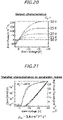
- FIG. 41 shows an example of the AFM measurement results of the electrodes for source/drain of the present disclosure.
- FIG. 41 is an AFM measurement result of the Au electrode having a surface roughness Rq of 0.6 nm with a PMMA protective film and a PVA handling film.
- the electrodes for source/drain of the present disclosure comprise 10 or more sets, preferably 50 or more sets, more preferably 1000 or more sets, even more preferably 10000 or more sets, and even more preferably 50000 or more sets of electrodes for source/drain.
- the first electrode 10, 20 from the top has a channel length L of 10 ⁇ m, and a channel width W of 500 ⁇ m.
- the second electrodes 12 and 22 from the top have a channel length L of 20 ⁇ m and a channel width W of 500 ⁇ m.
- the third electrodes 14 and 24 from the top have a channel length L of 40 ⁇ m and a channel width W of 500 ⁇ m.
- the channel length between the electrodes in each set of the electrodes for source/drain of the present disclosure is 200 ⁇ m or less, preferably 100 ⁇ m or less, more preferably 10 ⁇ m or less, even more preferably 1 ⁇ m or less, and even more preferably 0.5 ⁇ m or less.
- the channel length is a channel length in each electrode set (one element). In each of the ten or more pairs of electrodes, the channel length may be different from each other as long as it is 200 ⁇ m or less.
- the lower limit value of the channel length is not particularly limited, and may be preferably about 0.05 ⁇ m, which is about the same as the lower limit value of a thickness of a protective film described below.
- the organic semiconductor device comprising the electrodes for source/drain of the present disclosure can operate at a practical high frequency.
- the practical frequency is preferably 10 kHz or more, more preferably 100 kHz or more, even more preferably 1 MHz or more, and even more preferably 10 MHz or more.
- the channel length is an average value of values measured at three points in the channel width direction in each set (one element). The measurement positions of the three points are the positions of the center point and the two points on both sides of the center point, obtained by dividing the channel width into four equal parts.
- the channel width is not particularly limited, and may be, for example, 100 ⁇ m to 10000 ⁇ m.
- the electrodes for source/drain of the present disclosure have a surface having a surface roughness Rq of 2 nm or less.
- the surface 101 of the electrode 10 and the surface 201 of the electrode 20 have a surface roughness Rq of 2 nm or less.
- the surface roughness Rq of the electrode is preferably 1 nm or less, more preferably 0.5 nm or less.
- the lower limit value of the surface roughness Rq of the electrode is not particularly limited, and may be, for example, 0.1 nm.
- a surface having a surface roughness Rq of 2 nm or less is in contact with the organic semiconductor film.
- the surface roughness Rq of the surface of the organic semiconductor film in contact with the electrode is also small, preferably 2 nm or less.
- the surface roughness Rq of the organic semiconductor film is preferably 1 nm or less, more preferably 0.5 nm or less.
- the lower limit value of the surface roughness Rq of the organic semiconductor film is not particularly limited, and may be, for example, 0.1 nm.
- the surface roughness Rq of the electrode is the root-mean-square roughness of the value measured at three points using an atomic force microscope (AFM) on the surface of each pair of the electrodes (one element) in contact with the organic semiconductor film after separation from the release layer, and is the value of the square root of the value obtained by averaging the square of the deviation from the average line to the measurement curve.
- the measurement positions of the three points are the positions of the center point and the two points on both sides of the center point, obtained by dividing the longest line passing in the plane of the electrode into four equal portions.
- the longest line passing in the plane of the electrode is, for example, a diameter when the electrode is a circle, and a diagonal line when the electrode is rectangular.
- the parallelism of the channel length between the electrodes in each set is preferably 1 degree or less, more preferably 0.5 degrees or less, even more preferably 0.1 degrees or less, and even more preferably 0.01 degrees or less.
- the parallelism of the channel length is an angle formed by sides of opposing electrodes forming the channel length of each electrode set (one element). Since each set of electrodes is excellent in the parallelism of the channel length, the organic semiconductor device comprising the electrodes for source/drain of the present disclosure can exhibit characteristics as designed.
- the method for measuring the angle (parallelism) formed by the sides of the opposing electrodes is performed as follows: SEM observation of the channel length is performed at a magnification as large as possible within a range including the entire channel length and channel width of each pair of electrodes (one element). Based on the SEM image obtained by SEM observation, the channel width is divided into four equal portions in the channel width direction with respect to the sides (two sides) of the opposing electrodes of each electrode set (one element), the positions of the sides of the five points including the both ends of the channel width are measured, and a straight line in which the sum of the squares of the distances from the measured five points is minimized is specified by the least squares method. The angle formed by the two specified straight lines is measured, and the parallelism is calculated.
- the material of the electrode is not particularly limited as long as it is used in an organic semiconductor device, and preferably is Au, Ag, carbon, a conductive polymer, or a combination thereof, and more preferably is Au.
- the thickness of the electrode is preferably 20 to 200 nm, more preferably 25 to 100 nm, and even more preferably 30 to 50 nm.
- the electrodes for source/drain of the present disclosure are composed of an insulating polymer having a glass transition point of 80° C or more with a thickness of 1 ⁇ m or less, and further has a protective film attached to the surface of the electrode 10, 20 opposite to the surface 101, 201 by electrostatic force, and extending in at least a part of the channel.
- the protective film is composed of an insulating polymer having a glass transition point of 80° C or more and having no adhesiveness, it does not cause long-term damage to the organic semiconductor film, and the organic semiconductor does not easily change with time.
- the protective film is composed of an insulating polymer having a glass transition point of 80° C or more and having no adhesiveness, it does not cause long-term damage to the organic semiconductor film, and the organic semiconductor does not easily change with time.
- a thin film having a thickness of 1 ⁇ m or less an adhesive force due to an electrostatic force can be exhibited between the protective film and the electrode, and between the protective film and the organic semiconductor film.
- the change with time of the organic semiconductor is evaluated by measuring the value of the mobility of the semiconductor device comprising the organic semiconductor for a predetermined period, preferably 4 weeks or more, more preferably 8 weeks or more.
- FIG. 3 shows a cross-sectional schematic drawing of the electrodes 10 and 20 for source/drain of the present disclosure having the protective film 30.
- the thickness of the protective film 30 has a thickness of preferably 1 ⁇ m or less, more preferably less than 1 ⁇ m, and even more preferably 0.5 ⁇ m or less.
- the lower limit value of the thickness of the protective film is not particularly limited, but is 0.05 ⁇ m from the viewpoint of stably forming the insulating film.
- the glass transition point of the protective film 30 is 80° C or more, preferably 90° C or more, more preferably 100° C or more. Since the insulating polymer having the glass transition point in the range described above has the glass transition point sufficiently higher than the room temperature, when disposed in contact with the organic semiconductor film, the organic semiconductor film is unlikely to be deteriorated, and the organic semiconductor is unlikely to change with time.
- the protective film 30 adheres to the surfaces of the electrodes 10 and 20 opposite to the surfaces 101 and 201 by electrostatic force. As shown in FIG. 4 , the protective film 30 may extend in at least a part of the channel 40 which is a region indicated by the broken line between the electrodes 10 and 20. Preferably, the protective film 30 extends in substantially all regions of the channel 40 as shown in FIG. 3 .
- the protective film 30 does not substantially have an adhesive force, and substantially adheres to the electrodes 10 and 20 by an electrostatic force.
- the protective film 30 facilitates the handling of the electrode after the electrode is formed, prevents the electrode from being destroyed at the time of removing the handling film described later, and in the organic semiconductor device using the electrodes of the present disclosure, can suppress the electrode from peeling off from the organic semiconductor film.
- the material of the protective film 30 is preferably a fluorine-based polymer, such as polymethyl methacrylate (PMMA) having a glass transition point of about 100° C, CYTOP (registered trademark) having a glass transition point of about 108° C, or the like, polyparaxylylene (parylene (registered trademark)) having a glass transition point of about 109° C, or polyadamantyl methacrylate (PADMA) having a glass transition point of 200° C or more.
- PMMA polymethyl methacrylate
- CYTOP registered trademark
- PADMA polyadamantyl methacrylate
- the electrodes for source/drain of the present disclosure preferably comprise plating.
- the work function of the electrodes can be controlled, and carrier injection from the electrode to the organic semiconductor can be improved.
- the plating is preferably Au plating, Ag plating, Pt plating, or Cu plating, more preferably Au plating.
- the work function is photoelectron yield spectroscopy (PYS) and is measured by the following formula: Y 1 / 2 ⁇ hv - W F wherein Y is the photoelectron yield, h is the Planck constant, v is the frequency of the photons, and W F is the work function.
- PYS photoelectron yield spectroscopy
- the photoelectron yield representing the ratio of the number of emitted electrons to the number of irradiated photons is Y
- the energy of the irradiated light is hv
- the work function of a substance to be measured is W F
- Y 1/2 is plotted with respect to hv, and linear approximations are performed in each of regions before and after a portion which is considered to be W F .
- W F is obtained by obtaining an intersection point of two straight lines obtained thereby.
- FIG. 5 and FIG. 6 show cross-sectional schematic diagrams of the organic semiconductor devices 100 and 200 of the present disclosure comprising the gate electrode 54, the gate insulating film 52, the organic semiconductor film 66, and the electrodes 10 and 20 for source/drain.
- FIG. 5 is a cross-sectional schematic drawing of the top gate/top contact structure
- FIG. 6 is a cross-sectional schematic drawing of the bottom gate/top contact structure.
- the electrodes 10 and 20 are included as source/drain electrodes.
- the gate electrode 54 may be composed of a material of a gate electrode conventionally used, and may be, for example, doped-Si.
- the doped-Si can be one conventionally used as a gate electrode having a sufficiently low resistance value.
- the gate insulating film 52 may also be composed of a material of a gate insulating film conventionally used.
- the gate insulating film 52 may be integrally formed with the protective film 30 composed of an insulating polymer.
- the underlayer 56 can also be a layer including a substrate, a smoothed layer, and a surfacemodified layer, which are conventionally used.
- the underlayer 56 include glass, a glass substrate coated with a film, such as parylene (registered trademark) or trimethoxy(2-phenylethyl)silane ( ⁇ -PTS), a plastic substrate, such as polyethylene terephthalate (PET) or polyethylene naphthalate (PEN), a plastic substrate, such as PET or PEN whose surface is coated with a film, such as parylene (registered trademark), a substrate on which a device, such as a transistor is fabricated on the above substrate, or a substrate in which an interlayer insulating film, such as parylene (registered trademark) or alumina is deposited on the above device.
- a film such as parylene (registered trademark) or trimethoxy(2-phenylethyl)silane ( ⁇ -PTS)
- PET polyethylene
- the protective film 30 may be used as an insulating thin film as it is in the organic semiconductor devices 100 and 200, or the protective film 30 may be once dissolved to newly form the protective film 30, or the protective film 30 may be newly formed integrally with the gate insulating film 52.
- the surface roughness Rq of the surface of the organic semiconductor film in contact with the electrodes is 2 nm or less.
- the surface roughness Rq of the organic semiconductor film is the root-mean-square roughness of the value measured at three points on the surface of the organic semiconductor film using an atomic force microscope (AFM), and is the value of the square root of the value obtained by averaging the square of the deviation from the average line to the measurement curve.
- the measurement positions of the three points are the positions of the center point and the two points on both sides of the center point, obtained by dividing the longest line passing in the plane of the organic semiconductor film into four equal portions.
- the longest line passing in the plane of the organic semiconductor film is, for example, a diameter when the organic semiconductor film is a circle, and a diagonal line when the organic semiconductor film is a quadrangle.
- the contact resistance R C ⁇ W of the organic semiconductor device of the present disclosure is preferably 200 ⁇ cm or less, more preferably 175 ⁇ cm or less, even more preferably 150 ⁇ cm or less, and even more preferably 125 ⁇ cm or less.
- the Rc is the contact resistance
- the W is the channel width.
- the contact resistance of the organic semiconductor device is evaluated using the Transmission Line Method (TLM) method.
- TLM Transmission Line Method
- the R total ⁇ W is obtained by dividing the drain voltage V D by the drain current I D,lin in the transfer characteristics of the linear domain.
- the organic semiconductor device comprising the electrodes for source/drain of the present disclosure can be an organic EL (electroluminescence) element, an organic solar cell element, an organic photoelectric conversion element, an organic transistor element, an organic field effect transistor (OFET) element, or the like.
- organic EL electroluminescence
- OFET organic field effect transistor
- the present disclosure is also directed to a method for manufacturing electrodes for source/drain of an organic semiconductor device, the method comprising: preparing a substrate having a surface with a surface roughness Rq of 2 nm or less, forming a release layer on the surface of the substrate, forming 10 or more sets of electrodes for source/drain having a channel length of 200 ⁇ m or less on the release layer, forming a protective film on the release layer and the electrodes, forming a handling film on the protective film, separating an interface between the release layer and each of the electrodes and the protective film to obtain an electrode film comprising the electrodes, the protective film, and the handling film, and removing the handling film.
- electrodes for source/drain of an organic semiconductor device comprising 10 or more sets of electrodes, wherein a channel length between the electrodes in each set is 200 ⁇ m or less, and the electrodes in each set have a surface with a surface roughness Rq of 2 nm or less.
- a substrate having a surface roughness Rq of 2 nm or less is prepared.
- the surface roughness Rq of the substrate is preferably 1 nm or less, more preferably 0.5 nm or less.
- the lower limit value of the surface roughness Rq of the substrate is not particularly limited, and may be, for example, 0.1 nm. According to the method of the present disclosure, it is possible to obtain electrodes for source/drain having substantially the same surface roughness as the surface roughness Rq of the substrate.
- the surface roughness Rq of the substrate is the root-mean-square roughness of the value measured at three points on the surface of the substrate using an atomic force microscope (AFM), and is the value of the square root of the value obtained by averaging the square of the deviation from the average line to the measurement curve.
- the measurement positions of the three points are the positions of the center point and the two points on both sides of the center point, obtained by dividing the longest line passing in the plane of the substrate into four equal portions.
- the longest line passing in the plane of the substrate is, for example, a diameter when the substrate is a circle, and a diagonal line when the substrate is rectangular.
- the substrate having the above surface roughness Rq is preferably a glass substrate or a silicon substrate, and is, for example, EAGLE XG (registered trademark) manufactured by Corning.
- the substrate having the surface roughness Rq may be prepared by polishing a substrate, such as a glass substrate or a silicon substrate.
- the release layer is formed on the surface of the prepared substrate.
- An embodiment for forming the release layer preferably comprises: forming a hydroxyl group on the surface of the prepared substrate by subjecting the surface of the substrate to UV-ozone (UV/O 3 ), and subjecting the surface of the substrate on which the hydroxyl group is formed to self-assembled monolayer (SAM) treatment.
- UV-ozone UV-ozone
- SAM self-assembled monolayer
- UV ozone treatment By performing UV ozone treatment, an organic substance on the surface of the substrate is oxidized and removed, so that a hydroxyl group can be formed on the surface of the oxide film.
- oxygen (O 2 ) in the air can absorb ultraviolet rays having a wavelength of about 185 nm to generate ozone (O 3 ), the generated ozone (O 3 ) can absorb ultraviolet rays having a wavelength of about 254 nm to generate O 2 and active oxygen, and the active oxygen can oxidize and decompose organic substance on the surface of the substrate to form a hydroxyl group on the surface of the oxide film.
- FIG. 7 shows a cross-sectional schematic drawing of the substrate 60 on which the release layer 62 is formed by UV ozone treatment and SAM treatment.
- the SAM treatment is performed in order to adjust the surface energy.
- the release layer 62 is a film for separating electrodes and a protective film formed in a later step from the substrate 60.
- the release layer 62 remains on the substrate 60 side, and the electrodes and the protective film are separated.
- the release layer 62 is preferably a self-assembled monolayer.
- the adhesion force between the electrode and the self-assembled monolayer is weaker than the adhesion force between the electrode and the protective film, and the adhesion force between the protective film and the self-assembled monolayer is weaker than the adhesion force between the protective film and the handling film.
- the self-assembled monolayer preferably has a linear alkyl group or fluoroalkyl group, and the terminal group is an alkyl group, a fluoroalkyl group, a phenyl group, or a fluorophenyl group. Since such a self-assembled monolayer is a hydrophobic film having a contact angle of preferably 80 degrees or more, more preferably 90 degrees or more, and even more preferably 95 degrees or more, the electrodes and the protective film formed on the self-assembled monolayer in a later step can be easily separated.
- n is not particularly limited, and preferably is 8 to 18.
- CF linear fluoroalkyl group
- the self-assembled monolayer is, for example, decyltrimethoxysilane (DTS), triethoxy-1H, 1H, 2H, 2H-heptadecafluorodecylsilane (F-SAM), or trimethoxy(2-phenylethyl)silane ( ⁇ -PTS). Since DTS has a contact angle of about 101 degrees, F-SAM has a contact angle of about 110 degrees, and ⁇ -PTS has a contact angle of about 80 degrees, the electrodes and the protective film formed on the self-assembled monolayer in a later step can be more easily separated from the substrate.
- DTS decyltrimethoxysilane
- F-SAM triethoxy-1H, 1H, 2H, 2H-heptadecafluorodecylsilane
- ⁇ -PTS trimethoxy(2-phenylethyl)silane
- the SAM treatment can be performed by a vapor phase method or a liquid phase method.
- the vapor phase method is a method in which the substrate on which the hydroxyl group is formed is exposed to a saturated vapor of SAM molecules. Thereby, the SAM molecules and the hydroxyl group are dehydrated and condensed, and a self-assembled monolayer can be formed on the surface of the substrate.
- the exposure of the substrate to the saturated vapor of the SAM molecules can be performed, for example, by disposing the SAM solution and the substrate in a sealed container, forming a saturated vapor atmosphere of the SAM molecules by heating, and standing the substrate in the saturated vapor atmosphere of the SAM molecules.
- the standing time can be about 2 to 5 hours.
- the heating temperature can be about 120 to 150° C.
- the substrate is cleaned.
- DTS the substrate is washed with toluene, and then with 2-propanol.
- F-SAM the substrate is washed with 2-propanol.
- ⁇ -PTS the substrate is washed with toluene, and then with 2-propanol.
- the liquid phase method is a method in which the substrate on which the hydroxyl group is formed is immersed in a solution in which SAM molecules are dissolved. This method can also form a self-assembled monolayer on the surface of the substrate.
- FIG. 8 shows a cross-sectional schematic drawing of the substrate 60 on which the electrodes 10 and 20 are formed on the release layer 62.
- the method for forming the electrodes is not particularly limited, and a film or electrodes composed of an electrode material can be formed using a vacuum process or a solution process.
- electrodes can be formed on the release layer by a printing method, such as gravure offset printing, screen printing, or ink jet printing.
- a film of the electrode material can be coated on the release layer by vacuum deposition, spin coating, dip coating, roll coating, spray coating, flow coating, blade coating, push coating, or the like, and the formed film of the electrode material can be patterned using photolithography to form electrodes.
- the method for forming the electrodes may be selected depending on the electrode material.
- the electrode material is Au
- the electrodes are preferably formed by vacuum deposition and patterning using photolithography.
- the electrode is Ag
- the electrode is carbon
- the electrode is a conductive polymer
- Other embodiments for forming the release layer preferably comprise: forming a liquid-repellent polymer layer on the surface of the substrate; disposing a photomask or a metal mask on the substrate having the liquid-repellent polymer layer formed thereon; performing UV (ultraviolet light) irradiation on the substrate from the side on which the photomask or the metal mask is disposed to decompose the liquid-repellent polymer layer at the irradiated portion and form a hydroxyl group at the portion in which the liquid-repellent polymer layer is decomposed, and performing SAM treatment on the portion in which the hydroxyl group is formed.
- the forming 10 or more sets of electrodes for source/drain having a channel length of 200 ⁇ m or less comprises applying a conductive ink containing metal particles on the release layer, and performing electroless plating using the metal particles as a catalyst on the substrate on which the release layer coated with the conductive ink is formed to form 10 or more sets of electrodes for source/drain provided with plating having a channel length of 200 ⁇ m or less.
- the patterning of the electrodes is performed using the difference in wettability of the conductive ink between the liquid-repellent polymer layer and the portion in which the SAM treatment is performed.
- the liquid-repellent polymer layer can be formed on the surface of the substrate by a coating method.
- a coating method a method conventionally used can be used, and for example, an edge casting method, a continuous edge casting method, a drop casting method, a spin coating method, a printing method (ink jet method or gravure printing method), a dispenser method, a spray method, a dip coating method, a die coater method, a roll coater method, a bar coater method, a blade coating method, or the like can be used.
- the thickness of the liquid-repellent polymer layer is preferably 1 to 50 nm, more preferably 2 to 30 nm, even more preferably 3 to 20 nm, and even more preferably 5 to 15 nm. By having the preferable thickness of the liquid-repellent polymer layer, the surface roughness of the electrode to be formed can be reduced.
- the material of the liquid-repellent polymer layer is preferably a fluorine-based polymer, such as CYTOP (registered trademark), polytrifluoroethylene (PTFE), and perfluoroalkoxyalkane (PFA).
- CYTOP registered trademark
- PTFE polytrifluoroethylene
- PFA perfluoroalkoxyalkane
- the photomask or the metal mask disposed on the substrate on which the liquid-repellent polymer layer is formed is not particularly limited as long as it can block UV light, and can be made of chromium, for example.
- UV irradiation is performed on the substrate on which the liquid-repellent polymer layer is formed from the side on which the photomask or the metal mask is disposed, the liquid-repellent polymer layer at the irradiated portion is decomposed, and a hydroxyl group is formed at the portion in which the liquid-repellent polymer layer is decomposed.
- the surface becomes hydrophilic.
- the liquid-repellent polymer layer is decomposed by UV irradiation, but not all of the liquid-repellent polymer layer may be decomposed and a part may remain.
- the hydroxyl group can be formed on the substrate which is exposed by decomposition of the liquid-repellent polymer layer, on the remaining liquid-repellent polymer layer, or on both the exposed substrate and the remaining liquid-repellent polymer layer.
- the UV light is preferably vacuum ultraviolet light.
- the center wavelength of the vacuum ultraviolet light is about 10 to 200 nm.
- the SAM treatment is performed on the portion in which the hydroxyl group is generated by UV irradiation.
- the SAM treatment is performed on the entire substrate in which the hydroxyl group is generated by UV irradiation, but the self-assembled monolayer can be selectively formed only at a portion irradiated with UV.
- the self-assembled monolayer preferably has a linear alkyl group or fluoroalkyl group, and the terminal group is an alkyl group, a fluoroalkyl group, a phenyl group, or a fluorophenyl group.
- Such a self-assembled monolayer can easily separate electrodes formed on the self-assembled monolayer by coating and plating in later steps.
- n is not particularly limited, and preferably is 8 to 18.
- CF linear fluoroalkyl group
- the self-assembled monolayer is, for example, decyltrimethoxysilane (DTS), triethoxy-1H, 1H, 2H, 2H-heptadecafluorodecylsilane (F-SAM), or trimethoxy(2-phenylethyl)silane ( ⁇ -PTS), preferably F-SAM.
- DTS decyltrimethoxysilane
- F-SAM triethoxy-1H, 1H, 2H, 2H-heptadecafluorodecylsilane
- ⁇ -PTS trimethoxy(2-phenylethyl)silane
- a conductive ink containing metal particles is applied on the release layer.
- the method for applying the conductive ink is not particularly limited, and may be, for example, a blade coating method or the like.
- the conductive ink can be selectively applied only to the portion subjected to the SAM treatment. Since the portion subjected to the SAM treatment is lyophilic with respect to the solvent of the conductive ink and the photomask or the metal mask portion (liquid-repellent polymer layer) is liquid-repellent, the conductive ink can be selectively applied substantially only to the portion subjected to the SAM treatment.
- the metal particles of the conductive ink are preferably Ag, Au, Pt, Cu, Pd, Ni, or a combination thereof.
- the solvent of the conductive ink may be any solvent as long as the liquid-repellent polymer layer is relatively liquid-repellent and the portion subjected to the SAM treatment is relatively lyophilic.
- the solvent of the conductive ink is preferably a solvent in which the difference between the contact angle with the liquid-repellent polymer layer and the contact angle with the portion subjected to the SAM treatment is preferably 3° or more, more preferably 5° or more.
- the solvent of the conductive ink is more preferably an organic solvent of octane, toluene, tetradecane, butyl acetate, or a combination thereof.
- the solid content concentration in the solvent of the conductive ink is preferably 0.1 to 30 wt %.
- Electroless plating is performed using the metal particles of the applied conductive ink as a catalyst to form electrodes with plating.
- the work function of the electrode can be controlled, and carrier injection from the electrode to the organic semiconductor can be improved.
- plating is formed between the islandshaped metal particles, and the electrodes for source/drain having a surface roughness Rq of 2 nm or less can be obtained.
- the electrodes for source/drain comprise metal particles and plating.
- the plating is preferably Au plating, Ag plating, Pt plating, or Cu plating, more preferably Au plating.
- the electroless plating may be an autocatalytic reduction plating conventionally used.
- the plating solution contains a buffer material for preventing pH fluctuation, a complexing agent for stabilizing the metal ions, and the like.
- the metal ions in the plating solution can be precipitated by a reduction reaction using the metal particles as a catalyst to form a plating film.
- the electrodes can be formed by the above process, ten or more sets of fine electrodes having a channel length of 200 ⁇ m or less and a surface roughness Rq of 2 nm or less can be provided, and such electrodes can be applied to manufacturing of a practical integrated circuit of an organic semiconductor device. Further, after forming the electrodes on the release layer as described above, the electrodes can be separated from the release layer and disposed on the organic semiconductor film as described later, so that the organic semiconductor film is small in damage and does not easily change with time. In the method of the present disclosure, since the electrodes can be formed by the above process, it is possible to obtain the electrodes having a parallelism of the channel length of preferably 1 degree or less in each set of the plurality of sets of 10 or more.
- FIG. 9 shows a cross-sectional schematic drawing of the substrate 60, the release layer 62, and the electrodes 10 and 20 on which the protective film 30 is formed.
- the protective film 30 can suppress separation, damage, or the like of the electrodes when removing the handling film in a later step.
- the protective film can also suppress peeling of the electrodes from the organic semiconductor film in the organic semiconductor device comprising the electrodes manufactured by the method of the present disclosure.
- the protective film is composed of an insulating polymer having a thickness of 1 ⁇ m or less, is attached to a surface of the electrodes opposite to the surface of the electrodes by electrostatic force, and extends in at least a part of the channel.
- the protective film 30 can be a fluorine-based polymer, such as polymethyl methacrylate (PMMA) and CYTOP (registered trademark), polyparaxylylene (parylene (registered trademark)), or polyadamantyl methacrylate (PADMA), which does not affect the characteristics of the organic semiconductor film.
- PMMA polymethyl methacrylate
- CYTOP registered trademark
- polyparaxylylene parylene (registered trademark)
- PADMA polyadamantyl methacrylate
- the protective film 30 is preferably formed by a spin coating method or a chemical vapor deposition method.
- the protective film is preferably PMMA, CYTOP (registered trademark), or PADMA formed by a spin coating method.
- the spin coating method is convenient and preferable from a practical viewpoint.
- the conditions of the spin coating method such as the number of rotations, the time, and the like can be conventionally performed conditions, and may be appropriately set depending on the material of the protective film.
- the protective film is preferably polyparaxylylene (parylene (registered trademark)), which can be formed by a chemical vapor deposition method which is a dry process.
- the protective film of parylene (registered trademark) can further prevent the electrodes formed by the coating method from dissolving.
- the chemical vapor deposition method can be performed by a conventional method, and for example, the dimer is heated to 170° C to be evaporated, and further heated to 690° C to cleave the dimer to form a monomer.
- the formed monomer is then introduced into a chamber in which the substrate is placed and maintained at room temperature, and is rapidly cooled to form a polymer by radical polymerization on the surface of the substrate, thereby forming a film.
- FIG. 10 shows a cross-sectional schematic drawing of the substrate 60, the release layer 62, the electrodes 10 and 20, and the protective film 30 on which the handling film 64 is formed.
- the handling film 64 is formed as a handling film for separating the electrodes 10 and 20 and the protective film 30 from the release layer 62 as shown in FIG. 10 .
- the handling film 64 can also function as a handling film for disposing the electrode film having the protective film on the organic semiconductor film.
- the thickness of the handling film 64 is not particularly limited as long as it can handle the electrodes 10 and 20 and the protective film 30, but is preferably 10 ⁇ m or more.
- the upper limit of the thickness of the handling film 64 is not particularly limited, but is preferably 100 ⁇ m or less because the larger the thickness, the longer the removal of the handling film takes time.
- the handling film 64 is preferably a material corresponding to the protective film 30.
- the handling film 64 is preferably a water-soluble polymer film.
- the handling film 64 is preferably an organic solvent-soluble polymer film. Since the handling film 64 is the preferable polymer film, the handling film can be easily removed by dissolving only the handling film 64 without dissolving the protective film 30 in the solution process.
- the handling film 64 is a water-soluble polymer film
- an aqueous solution of a water-soluble polymer is applied on the protective film to form a water-soluble polymer film.
- the water-soluble polymer film can be removed by dissolving it in water after the electrodes 10 and 20 and the protective film 30 are separated from the release layer 62.
- the electrode film, the protective film, and the handling film are disposed on the organic semiconductor film without removing the handling film 64 in the sequence step, the water-soluble polymer film can be removed by dissolving it in water after the electrode film and the protective film are disposed on the organic semiconductor film.
- the water-soluble polymer of the water-soluble polymer film is preferably polyvinyl alcohol (PVA), polyacrylic acid, dextran, or polymethacrylic acid, more preferably polyvinyl alcohol (PVA).
- PVA polyvinyl alcohol
- PVA polyacrylic acid
- dextran dextran
- Pmethacrylic acid more preferably polyvinyl alcohol (PVA).
- the handling film 64 is an organic solvent-soluble polymer film
- an aqueous solution of the organic solvent-soluble polymer is applied on the protective film to form an organic solvent-soluble polymer film.
- the organic solvent-soluble polymer film can be removed by dissolving it in an organic solvent after the electrodes 10 and 20 and the protective film 30 are separated from the release layer 62.
- the organic solvent soluble polymer film can be removed by dissolving it in an organic solvent after the electrode and the protective film are disposed on the organic semiconductor film.
- the organic solvent-soluble polymer of the organic solvent-soluble polymer film is preferably polymethyl methacrylate (PMMA), polystyrene (PS), polyacrylonitrile (PAN), or polyethylene (PE), more preferably polymethyl methacrylate (PMMA).
- PMMA polymethyl methacrylate
- PS polystyrene
- PAN polyacrylonitrile
- PE polyethylene
- the interface between the release layer and the electrode and the protective film is separated to obtain an electrode film comprising the electrode, the protective film, and the handling film.
- FIG. 10 is a cross-sectional schematic drawing of the electrode film 600 in which the protective film 30 is sandwiched between the electrodes 10 and 20 and the handling film 64.
- FIG. 13 shows an external photograph of an electrode film in which a PMMA film as a protective film is sandwiched between an Au electrode and a PVA film of a water-soluble polymer.
- FIG. 14 shows an enlarged microscopic photograph of the Au electrode pattern of FIG. 13 .
- the first to third electrodes from the top of FIG. 14 have a channel width of 500 ⁇ m, and channel lengths of 10 ⁇ m, 20 ⁇ m, and 40 ⁇ m, respectively.
- the handling film 64 is removed from the electrode film 600.
- the removal of the handling film 64 can be performed by a method depending on the material constituting the handling film.
- the handling film is composed of a water-soluble polymer
- water is applied to the electrode film to remove the handling film.
- water When water is applied to remove the handling film, preferably, water is first dropped on the handling film, and when the handling film is substantially peeled off, water is added until the entire electrode film is immersed, and the water in which the electrode film is immersed is stirred until the handling film is dissolved to be substantially removed from the electrode film.
- the protective film By removing the handling film, electrodes on which the protective film is disposed can be obtained.
- the protective film When the protective film is composed of a non-water-soluble polymer, it may be removed by an organic solvent, such as acetonitrile.
- the protective film When the protective film is composed of a polymer that is not dissolved in an organic solvent, it may be removed by a solvent, such as a fluorine-based solvent.
- a solvent for dissolving the protective film may be used depending on the type of the polymer constituting the protective film.
- the present disclosure is also directed to a method for manufacturing an organic semiconductor device, comprising: preparing a substrate having a surface roughness Rq of 2 nm or less, forming a release layer on the surface of the substrate, forming 10 or more sets of electrodes for source/drain having a channel length of 200 ⁇ m or less on the release layer, forming a protective film on the release layer and the electrodes, forming a handling film on the protective film, separating an interface between the release layer and the electrodes and the protective film to obtain an electrode film comprising the electrodes, the protective film, and the handling film, disposing the electrode film on the organic semiconductor film, and removing the handling film.
- the electrode film 600 obtained in the above method for manufacturing electrodes for source/drain of the organic semiconductor device is disposed on the organic semiconductor film 66.
- the electrode film and the organic semiconductor film are brought into contact with each other so that the protective film 30 and the organic semiconductor film 66 are in close contact with each other.
- FIG. 12 is a cross-sectional schematic drawing of an example of an organic semiconductor device 200 in which an electrode film 600 comprising the electrodes 10 and 20, the protective film 30, and the handling film 64 is disposed on the organic semiconductor film 66. After disposing the electrode film 600 on the organic semiconductor film 66, the handling film 64 is removed.
- the organic semiconductor device 200 is an organic field-effect transistor having a bottom gate/top contact structure.
- the organic semiconductor film 66 is formed on the gate electrode 74 and the underlying layers (gate insulating films) 70 and 72.
- the gate electrode 74 can be a material conventionally used, for example, doped-Si or the like.
- the underlying layers 70 and 72 can also be materials conventionally used, such as SiO 2 , parylene (registered trademark), or the like.
- the electrode film 600 When disposing the electrode film 600 on the organic semiconductor film 66, it is preferable to heat the temperature of the organic semiconductor film 66 to 50 to 90° C, more preferably 60 to 80° C.
- the heating may be performed using a hot plate or the like.
- the protective film 30 and the handling film 64 By heating the organic semiconductor film 66 to the preferable temperature, the protective film 30 and the handling film 64 become soft, it becomes easier to dispose the protective film 30 along the surface shape of the electrodes 10 and 20 and so as to adhere to the surface of the organic semiconductor film 66, and the adhesion between the protective film 30 and the organic semiconductor film 66 is improved.
- the entire substrate on which the organic semiconductor film 66 is disposed can be heated.
- the organic semiconductor film 66 is heated from the substrate side.
- the electrode film 600 After disposing the electrode film 600 on the organic semiconductor film 66, it is possible to more favorably dispose the protective film 30 so as to adhere to the surface of the organic semiconductor film 66 along the surface shape of the electrodes 10 and 20, and it is possible to further improve the adhesion between the protective film 30 and the organic semiconductor film 66.
- the handling film 64 is removed.
- the removal of the handling film 64 can be performed by a method depending on the material constituting the handling film.
- the handling film is composed of a water-soluble polymer
- water is applied to the electrode film disposed on the organic semiconductor film while the substrate, the organic semiconductor film, and the electrode film are heated to remove the handling film.
- the temperature of the film may be lowered to 20 to 40° C.
- the application of water to the electrode film preferably initially drops water on the handling film, and when the handling film is substantially peeled off, water is added until the entire electrode film is immersed, and the water in which the electrode film is immersed is stirred until the handling film is dissolved to be substantially removed from the electrode film.
- FIG. 15 shows an external photograph of the obtained organic semiconductor device.
- Au electrodes and a protective film of PMMA are formed on the organic semiconductor film.
- an organic semiconductor device such as an organic field-effect transistor, can be manufactured without damaging the organic semiconductor layer.
- the organic semiconductor film is preferably an organic semiconductor single crystal film.
- the average film thickness of the organic semiconductor single crystal film is 2 to 100 nm, preferably 4 to 20 nm. By having the average film thickness of the organic semiconductor single crystal film in the range, good device characteristics can be obtained.
- the average film thickness of the organic semiconductor single crystal film can be measured using a stylus type surface profile measuring instrument or an atomic force microscope.
- the organic semiconductor single crystal film preferably has 1 molecular layer (monolayer) to 50 molecular layers, more preferably 1 molecular layer to 10 molecular layers, still more preferably 1 molecular layer to 5 molecular layers, and still more preferably 1 molecular layer to 3 molecular layers in the thickness direction.
- the organic semiconductor single crystal film most preferably has one molecular layer, but may have two or more molecular layers in the thickness direction. The number of molecular layers of the organic semiconductor single crystal film can be measured by an atomic force microscope.
- the contact resistance is the sum of two kinds of resistance: the resistance of the bulk region of the organic semiconductor in the charge transport from the electrode/organic semiconductor interface to the channel region, and the resistance in the charge injection from the electrode to the organic semiconductor layer.
- the channel region in which carriers are accumulated corresponds to one layer to several molecular layers of the organic semiconductor layer at the interface of the gate insulating film, and the other layers prevent smooth carrier injection from the electrode to the channel.
- the organic semiconductor device since the electrodes formed on the flat substrate are disposed on the organic semiconductor film, thermal damage such as that applied in the vapor deposition process or damage due to a resist, an etchant, or the like during the photolithography process is not applied to the organic semiconductor film. Therefore, the organic semiconductor device operates well as without damaging the organic semiconductor film even if the organic semiconductor film is an organic semiconductor single crystal film with one molecular layer in the thickness direction.
- the thickness of one molecular layer of the organic semiconductor single crystal film is preferably 2 to 6 nm, more preferably 2 to 4 nm.
- the thickness of one molecular layer of the organic semiconductor single crystal film can be measured by combining single crystal X-ray structure analysis and atomic force microscope observation.
- the area of the organic semiconducting single-crystal film is preferably 2 mm 2 or more, more preferably 10 mm 2 or more, even more preferably 100 mm 2 or more, even more preferably 1000 mm 2 or more, and even more preferably 10000 mm 2 or more.
- the upper limit of the area of the organic semiconductor single crystal film is not particularly limited, and may be limited by the size of the manufacturing facility and may be, for example, 10 m 2 . Conventionally, when a vapor phase growth method is used, only an organic semiconductor single crystal film having an area of at most about 1 mm 2 could be obtained, whereas the organic semiconductor device of the present disclosure can have a large area as described above.
- the organic semiconductor single crystal film is composed of a single domain or multi-domain, and preferably is composed of a single domain.
- the domain of the organic semiconductor single crystal film can be measured by single crystal X-ray diffraction.
- the organic semiconductor single crystal film preferably has a single domain with a contiguous area of 0.005 mm 2 or more, more preferably 0.5 mm 2 or more, and even more preferably 2.0 mm 2 or more.
- the organic semiconductor single crystal film exhibits a mobility of preferably 0.5 cm 2 /V•s or more, more preferably 3.0 cm 2 /V•s or more, even more preferably 5.0 cm 2 /V•s or more, even more preferably 7.5 cm 2 /V•s or more, and even more preferably 10 cm 2 /V•s or more.
- the mobility of the organic semiconductor single crystal film can be calculated from the measurement results of the organic field effect transistor.
- the type of the organic semiconductor constituting the organic semiconductor film is not particularly limited, and for example, a polycyclic aromatic compound of four or more rings, or a polycyclic compound of four or more rings formed of one or more unsaturated five-membered heterocyclic compounds and a plurality of benzene rings can be used.
- the organic semiconductor constituting the organic semiconductor film is preferably a material having a high self-aggregation ability, such as a p-type organic semiconductor Cn-DNBDT-NW of the following formula (1) exhibiting a high mobility.
- n may be 1 to 14.
- the self-aggregation ability refers to a tendency of molecules to spontaneously aggregate and crystallize as the molecules precipitate from a solvent.
- R1 and R2 are each independently a hydrogen atom or an alkyl group having 4 to 10 carbon atoms.
- the alkyl group may comprise a heteroatom (typically selected from an oxygen atom and a sulfur atom).
- R1 and R2 together can form a ring.
- R1 and R2 are each independently a hydrogen atom or an alkyl group having 5 to 8 carbon atoms. More preferably, each of R1 and R2 is independently a hydrogen atom or a hexyl group.
- the n represents an integer of 5 to 100.
- the n indicates the average number of thiophene monomer units in the polythiophene semiconductor, i.e., the length of the polythiophene chain. From the viewpoint of forming the single crystal film, the n is preferably 50 or less.
- each of R3, R4, R5 and R6 is independently a hydrogen atom or an alkyl group having 1 to 14 carbon atoms.
- the alkyl group may comprise a heteroatom (typically selected from an oxygen atom and a sulfur atom), and the hydrogen atom in the alkyl group may be substituted with a substituent, such as a halogen atom.
- R4 and R5 are hydrogen atoms
- R3 and R6 are each independently an alkyl group having 1 to 14 carbon atoms
- R3 and R6 are hydrogen atoms
- R4 and R5 are each independently an alkyl group having 1 to 14 carbon atoms.
- R3 and R6 are hydrogen atoms
- R4 and R5 are each independently an alkyl group having 1 to 14 carbon atoms.
- the carbon number of the alkyl group is preferably from 4 to 12, more preferably from 6 to 10.
- each of R7, R8, R9 and R10 is independently a hydrogen atom or an alkyl group having 1 to 14 carbon atoms.
- the alkyl group may comprise a heteroatom (typically selected from an oxygen atom and a sulfur atom), and the hydrogen atom in the alkyl group may be substituted with a substituent, such as a halogen atom.
- R7 and R9 are hydrogen atoms
- R8 and R10 are each independently an alkyl group having 1 to 14 carbon atoms
- R8 and R10 are hydrogen atoms
- R7 and R9 are each independently an alkyl group having 1 to 14 carbon atoms.
- R8 and R10 are hydrogen atoms
- R7 and R9 are each independently an alkyl group having 1 to 14 carbon atoms.
- the carbon number of the alkyl group is preferably from 6 to 13, more preferably from 8 to 10.
- each of R11, R12, R13 and R14 is independently a hydrogen atom or an alkyl group having 1 to 14 carbon atoms.
- the alkyl group may comprise a heteroatom (typically selected from an oxygen atom and a sulfur atom), and the hydrogen atom in the alkyl group may be substituted with a substituent, such as a halogen atom.
- R11 and R13 are hydrogen atoms
- R12 and R14 are each independently an alkyl group having 1 to 14 carbon atoms
- R12 and R14 are hydrogen atoms
- R11 and R13 are each independently an alkyl group having 1 to 14 carbon atoms.
- R12 and R14 are hydrogen atoms
- R11 and R13 are each independently an alkyl group having 1 to 14 carbon atoms.
- the number of carbon atoms of the alkyl group is preferably from 5 to 12, more preferably from 8 to 10.
- R15, R16, R17 and R18 are each independently a hydrogen atom or an alkyl group having 1 to 14 carbon atoms.
- the alkyl group may comprise a heteroatom (typically selected from an oxygen atom and a sulfur atom), and the hydrogen atom in the alkyl group may be substituted with a substituent, such as a halogen atom.
- R16 and R18 are hydrogen atoms, and R15 and R17 are each independently an alkyl group having 1 to 14 carbon atoms, or R15 and R17 are hydrogen atoms, and R16 and R18 are each independently an alkyl group having 1 to 14 carbon atoms. More preferably, R16 and R18 are hydrogen atoms, and R15 and R17 are each independently an alkyl group having 1 to 14 carbon atoms.
- the number of carbon atoms of the alkyl group is preferably from 5 to 12, more preferably from 8 to 10.
- R may be linear alkyl, branched alkyl, fluorinated linear/branched alkyl, triisopropylsilylethynyl, phenyl, or the like.
- the organic semiconductor film is a single crystal can be confirmed by observation with a transmission electron microscope (TEM).
- TEM transmission electron microscope
- the organic semiconductor single crystal film can be formed by a coating method.
- a coating method a method conventionally used can be used, and for example, an edge casting method, a continuous edge casting method, a drop casting method, a spin coating method, a printing method (ink jet method or gravure printing method), a dispenser method, a spray method, a dip coating method, a die coater method, a roll coater method, a bar coater method, a blade coating method, or the like can be used.
- the continuous edge casting method is preferable because it can obtain an organic semiconductor single crystal film having a thickness in which the film thickness is controlled to be very thin, and it is easy to control the thickness to about 1 molecular layer to 3 molecular layers.
- a carrier injection promoting film is disposed between the electrode and the organic semiconductor film.
- the carrier injection promoting film By disposing the carrier injection promoting film between the electrode and the organic semiconductor film, injection of carriers into the organic semiconductor film can be promoted.
- the carrier injection promoting film may be disposed in an island shape between the electrodes and the organic semiconductor film.
- the thickness of the carrier injection promoting film is preferably 1 to 4 nm, more preferably 2 to 3 nm.
- a carrier injection promoting layer is formed on the release layer, an electrode material is vacuum-deposited on the carrier injection promoting layer, and patterning is performed by photolithography.
- the protective film is then separated, and the carrier injection promoting layer, the electrodes, and the protective film can be disposed so that the carrier injection promoting layer is in contact with the organic semiconductor film.
- a conductive ink may be applied on the carrier injection promoting layer, and then electroless plating may be performed to form electrodes.
- the carrier injection promoting layer is preferably 2,3,5,6-tetrafluoro-7,7,8,8-tetracyanoquinodimethane (F4-TCNQ).
- the carrier injection promoting layer can be formed on the release layer by vacuum deposition.
- the surface of the electrode may be modified with a self-assembled monolayer, such as pentafluorobenzenethiol (PFBT) or 4-methylbenzenethiol (MBT).
- PFBT pentafluorobenzenethiol
- MBT 4-methylbenzenethiol
- the separated electrode film is immersed in ethanol in which PFBT or MBT is dissolved.
- PFBT or MBT can be formed on the electrode surface.
- an Eagle glass (EAGLE XG (registered trademark) of Corning) was prepared and subjected to UV-ozone (UV/O 3 ) treatment to form a hydroxyl group on the glass surface.
- UV-ozone treatment was performed by UV irradiation for 15 minutes under an oxygen atmosphere using UV lamps UV 253H (wavelengths of 184.9 nm and 253.7 nm) manufactured by Filgen Corporation.
- the glass substrate on which the hydroxyl group was formed was subjected to SAM treatment, and a self-assembled monolayer of decyltrimethoxysilane (DTS) was formed as a release layer on the surface of the glass substrate.
- DTS decyltrimethoxysilane
- the SAM treatment was performed by disposing the DTS solution and the glass substrate on which the hydroxyl group was formed in a sealed container, heating to 120° C to form a saturated vapor atmosphere of the DTS molecules, standing the glass substrate on which the hydroxyl group was formed in the saturated vapor atmosphere of the DTS molecules for 3 hours, and washing the glass substrate with toluene followed by washing with 2-propanol.
- the number of rotations was increased to 500 rpm in 1 second, held at 500 rpm for 5 seconds, and held at 2000 rpm for 40 seconds. The rotation was stopped, and the substrate was dried at 80° C for 30 minutes to remove the solvent to form a protective film of PMMA having a thickness of 75 nm.
- PVA polyvinyl alcohol
- FIG. 13 shows an external photograph of the electrode film in which the PMMA protective film was sandwiched between the Au electrodes and the PVA handling film.
- FIG. 14 shows an enlarged microscopic photograph of the Au electrode pattern of FIG. 13 .
- the first to third electrodes from the top of FIG. 14 have a channel width of 500 ⁇ m, and channel lengths of 10 ⁇ m, 20 ⁇ m, and 40 ⁇ m, respectively.
- the electrode film comprising the Au electrode, the PMMA protective film, and the PVA handling film was disposed on the glass plate so that the Au electrodes were fixed using a weight. Water was then dropped on the PVA handling film, and after the handling film was substantially peeled off, the temperature was lowered to 30° C, water was added until the entire electrode film was immersed, and the water in which the electrode film was immersed was stirred for 3 hours until the PVA was completely dissolved to remove the handling film, thereby fabricating Au electrodes having a PMMA protective film as shown in FIG. 4 .
- the Au electrodes having the PMMA protective film was immersed in acetonitrile at 30° C for 30 minutes to remove the PMMA protective film, and Au electrodes as shown in FIG. 2 were manufactured.
- the channel length/channel width of the electrodes in each set of the obtained Au electrodes 64 was 100 ⁇ m/500 ⁇ m, 80 ⁇ m/500 ⁇ m, 60 ⁇ m/500 ⁇ m, 40 ⁇ m/500 ⁇ m, 20 ⁇ m/500 ⁇ m, and 10 ⁇ m/500 ⁇ m, respectively, and the surface roughness Rq of the electrodes was 0.6 nm.
- the parallelism of the channel length in each set of electrodes (one element) was 0.1 degrees or less.
- FIG. 31 shows an enlarged photograph of a pair of electrodes for source/drain surrounded by a broken line in FIG. 30 .
- the channel length/channel width of the electrode in each set of the obtained 50 sets of Au electrodes was 200 ⁇ m/1000 ⁇ m, and the surface roughness Rq of the electrodes was 0.6 nm.
- the parallelism of the channel length in each set of electrodes (one element) was 0.1 degrees or less.
- An electrode film comprising Au electrodes, a PMMA protective film, and a PVA handling film was obtained in the same manner as in Example 1.
- organic semiconductor As an organic semiconductor, a powder of p-type organic semiconductor C 9 -DNBDT-NW of the following formula (16): exhibiting high mobility was prepared. 3-chlorothiophene was used as a solvent, and the organic semiconductor powder was dissolved in the solvent to prepare an organic semiconductor solution.
- a substrate in which doped-Si as a gate electrode having a thickness of 500 ⁇ m, an SiO 2 having a thickness of 100 nm, and parylene (diX-SR (registered trademark)) having a thickness of 70nm were laminated was prepared.
- the prepared organic semiconductor solution was applied on the substrate heated to 80° C by the continuous edge casting method to form an organic semiconductor single crystal film of a monolayer on the substrate.
- the surface roughness Rq of the organic semiconductor film was 0.2 nm.
- the laminate of the obtained doped-Si, SiO 2 , parylene (diX-SR (registered trademark)), and the organic semiconductor film was disposed on the hot plate, and the electrode film was disposed on the organic semiconductor film so that the electrodes were in contact with the organic semiconductor film as schematically shown in FIG. 12 while being heated to 80° C.
- FIG. 18 shows a graph of the transfer characteristics representing the relationship between the gate voltage and the drain current in the saturation region
- FIG. 19 shows a graph of the transfer characteristics representing the relationship between the gate voltage and the drain current in the linear region
- FIG. 20 shows a graph of the output characteristics representing the relationship between the drain voltage and the drain current depending on the gate voltage.
- the mobility in the saturated region was 10 cm 2 /V ⁇ s
- the mobility in the linear region was 10 cm 2 /V ⁇ s, which were very large mobility.
- theoretical values were used for the capacitance of the insulating film in which the SiO 2 and the parylene (registered trademark) were laminated.
- FIG. 21 shows a graph of the transfer characteristics representing the relationship between the gate voltage and the drain current in the saturation region
- FIG. 22 shows a graph of the transfer characteristics representing the relationship between the gate voltage and the drain current in the linear region
- FIG. 23 shows a graph of the output characteristics representing the relationship between the drain voltage and the drain current depending on the gate voltage.
- the mobility in the saturated region was 3.6 cm 2 /V ⁇ s
- the mobility in the linear region was 7.2 cm 2 /V ⁇ s
- good mobility was obtained even in a short channel device having a channel length of 10 ⁇ m.
- Organic semiconductor devices were manufactured in the same manner as in Example 3 except that the release layer was changed to triethoxy-1H, 1H, 2H, 2H-heptadecafluorodecylsilane (F-SAM).
- the mobility of the manufactured transistor having a channel length/channel width of 100 ⁇ m/500 ⁇ m was measured, and the same mobility as in Example 3 was shown.
- diX-SR registered trademark
- FIG. 16 shows a laser confocal microscopic photograph of the organic semiconductor (C 9 -DNBDT-NW) film observed from the top surface of the fabricated organic semiconductor device.
- a single-crystalline domain thin film of a monolayer was obtained on the entire surface (area: 450 mm 2 ) surrounded by a broken line.
- FIG. 17 shows the results of measuring the monolayer film of the C 9 -DNBDT-NW of FIG. 16 by atomic force microscopy (AFM). A thickness of 4nm corresponding to one molecular layer of C 9 -DNBDT-NW was obtained.
- FIG. 24 shows a graph of the transfer characteristics representing the relationship between the gate voltage and the drain current in the saturation region
- FIG. 25 shows a graph of the transfer characteristics representing the relationship between the gate voltage and the drain current in the linear region
- FIG. 26 shows a graph of the output characteristics representing the relationship between the drain voltage and the drain current depending on the gate voltage.
- the mobility in the saturated region was 15.3 cm 2 /V ⁇ s
- the mobility in the linear region was 11.6 cm 2 /V ⁇ s, and a transistor having very large mobility could be manufactured even if the organic semiconducting film was single-crystal of a monolayer.
- Organic semiconductor devices were manufactured in the same manner as in Example 3 except that a carrier injection promoting layer of 2,3,5,6-tetrafluoro-7,7,8,8-tetracyanoquinodimethane (F4-TCNQ) was formed on the release layer by vacuum deposition and Au electrodes were formed on the carrier injection promoting layer in the same manner as in Example 3.
- F4-TCNQ 2,3,5,6-tetrafluoro-7,7,8,8-tetracyanoquinodimethane
- FIG. 27 shows a graph of the transfer characteristics representing the relationship between the gate voltage and the drain current in the saturation region
- FIG. 28 shows a graph of the transfer characteristics representing the relationship between the gate voltage and the drain current in the linear region
- FIG. 29 shows a graph of the output characteristics representing the relationship between the drain voltage and the drain current depending on the gate voltage.
- the mobility in the saturated region was 2 cm 2 /V ⁇ s
- the mobility in the linear region was 5.4 cm 2 /V ⁇ s, and good mobility was obtained.
- Organic semiconductor devices were manufactured in the same manner as in Example 3 except that the release layer was changed to triethoxy-1H, 1H, 2H, 2H-heptadecafluorodecylsilane (F-SAM), the protective film was changed to CTX-809SP2 having a glass transition point of 108° C in which a terminal group of CYTOP (registered trademark) is CF 3, and parylene (diX-SR (registered trademark)) in the laminate was changed to ⁇ -PTS to obtain a laminate of doped-Si, SiO 2 , ⁇ -PTS, and an organic semiconductor film.
- F-SAM triethoxy-1H, 1H, 2H, 2H-heptadecafluorodecylsilane
- CTX-809SP2 having a glass transition point of 108° C in which a terminal group of CYTOP (registered trademark) is CF 3
- the CTX-809SP2 protective film of CYTOP (registered trademark) was formed in the following manner.
- a solution prepared by CTX-809SP2:CT-Solv.180 (solvent for dilution) 2:3 (mass ratio) was spin-coated on a glass substrate on which the Au electrodes were formed under the same conditions as in Example 1. The rotation was stopped, and the solvent was removed by drying at 50° C for 1 minute, and then at 80° C for 40 minutes, thereby forming an 809SP2 protective film having a thickness of 300 nm.
- the surface of CTX-809SP2 was modified by excimer light, and a PVA handling film was formed in the same manner as in Example 1.
- FIG. 32 shows a graph of the transfer characteristics representing the relationship between the gate voltage and the drain current in the saturation region
- FIG. 33 shows a graph of the transfer characteristics representing the relationship between the gate voltage and the drain current in the linear region
- FIG. 34 shows a graph of the output characteristics representing the relationship between the drain voltage and the drain current depending on the gate voltage.
- the mobility in the saturated region was 12 cm 2 /V ⁇ s
- the mobility in the linear region was 13 cm 2 /V ⁇ s, and good mobility was obtained.
- Organic semiconductor devices were manufactured in the same manner as in Example 8 except that a total of 112 sets of Au electrodes each having a channel length/channel width of 100 ⁇ m/500 ⁇ m, 80 ⁇ m/500 ⁇ m, 60 ⁇ m/500 ⁇ m, 40 ⁇ m/500 ⁇ m, 20 ⁇ m/500 ⁇ m, 10 ⁇ m/500 ⁇ m, and 200 ⁇ m/500 ⁇ m were formed, and the protective film was changed to CTL-809M having a glass transition point of 108° C in which a terminal group of CYTOP (registered trademark) is -CONH-Si(OR)n.
- CYTOP registered trademark
- the CTL-809M protective film was formed by the following method.
- the surface of the CTL-809M protective film was modified by excimer light, and a PVA handling film was formed in the same manner as in Example 1.
- FIG. 35 shows a graph of the transfer characteristics representing the relationship between the gate voltage and the drain current in the saturation region
- FIG. 36 shows a graph of the transfer characteristics representing the relationship between the gate voltage and the drain current in the linear region
- FIG. 37 shows a graph of the output characteristics representing the relationship between the drain voltage and the drain current depending on the gate voltage.
- the mobility in the saturated region was 15 cm 2 /V ⁇ s
- the mobility in the linear region was 11 cm 2 /V ⁇ s, and good mobility was obtained.
- Organic semiconductor devices were manufactured in the same manner as in Example 3 except that the protective film was changed to polyadamantyl methacrylate (PADMA) having a glass transition point of 200° C or more.
- PADMA polyadamantyl methacrylate
- the protective film of PADMA was formed by the following method. A solution in which 2 mass % of PADMA was dissolved in cyclohexane was spin-coated on a glass substrate on which Au electrodes were formed under the same conditions as in Example 1. The rotation was stopped, and the solvent was dried at 50° C for 30 seconds, and then dried at 80° C for 15 minutes to remove the solvent, thereby forming a PADMA protective film having a thickness of 200 nm.
- FIG. 38 shows a graph of the transfer characteristics representing the relationship between the gate voltage and the drain current in the saturation region
- FIG. 39 shows a graph of the transfer characteristics representing the relationship between the gate voltage and the drain current in the linear region
- FIG. 40 shows a graph of the output characteristics representing the relationship between the drain voltage and the drain current depending on the gate voltage.
- the mobility in the saturated region was 4.7 cm 2 /V ⁇ s
- the mobility in the linear region was 7.0 cm 2 /V ⁇ s, indicating good mobility.
- Organic semiconductor devices having a cross-sectional structure schematically shown in FIG. 43 were manufactured in the same manner as in Example 6 except that a total of 48 sets of 8 sets each of Au electrodes having channel lengths/channel widths of 100 ⁇ m/500 ⁇ m, 80 ⁇ m/500 ⁇ m, 60 ⁇ m/500 ⁇ m, 40 ⁇ m/500 ⁇ m, 20 ⁇ m/500 ⁇ m, and 10 ⁇ m/500 ⁇ m were formed in total in the same manner as in Example 1.
- FIG. 44 shows a graph showing the relationship between the channel length L and the R total ⁇ W for each of the V G -V th .
- FIG. 45 shows a graph showing the relationship between the V G -V th and the R C ⁇ W. From FIG. 45 , it was confirmed that a low contact resistance of R C ⁇ W of 175 ⁇ cm or less was obtained.
- an Eagle glass (EAGLE XG (registered trademark) from Corning) substrate was prepared, and as shown schematically in FIG. 46 , CYTOP (registered trademark) of CTL-809M having a thickness of 10 nm in which a terminal group is -CONH-Si(OR)n was formed as a liquid-repellent polymer layer 80 on the surface of the substrate 60.
- EAGLE XG Eagle glass
- CYTOP registered trademark of CTL-809M having a thickness of 10 nm in which a terminal group is -CONH-Si(OR)n was formed as a liquid-repellent polymer layer 80 on the surface of the substrate 60.
- the CTL-809M liquid-repellent polymer layer was formed by the following method.
- the number of rotations was increased to 500 rpm in 1 second, held at 500 rpm for 10 seconds, and held at 1000 rpm for 40 seconds.
- the rotation was stopped, and the solvent was removed by drying at 50° C for 1 minute, then at 80° C for 15 minutes, and further at 130° C for 40 minutes, thereby forming an 809M liquid-repellent polymer layer having a thickness of 10 nm.
- a chromium photomask 82 was disposed on the glass substrate on which the liquid-repellent polymer layer 80 was formed, and vacuum ultraviolet light (VUV) 84 was irradiated from the side on which the photomask 82 was disposed.
- VUV vacuum ultraviolet light
- FIG. 48 the liquid-repellent polymer layer 80 in the irradiated portion was decomposed, and a hydroxyl group was formed in the portion in which the liquid-repellent polymer layer was decomposed.
- the vacuum-ultraviolet light was irradiated in an N2 flowatmosphere using SUS1001 (manufactured by Ushio Electric Co., Ltd.) while moving an excimer lamp (wave length: 172 nm) at a rate of 0.04 mm/sec.
- SAM treatment was performed on the surface of the glass substrate 60 on which the hydroxyl group was formed using the vapor phase method, and a fluorine-based self-assembled monolayer 86 of triethoxy-1H, 1H, 2H, 2H-heptadecafluorodecylsilane (F-SAM) was formed on the surface.
- F-SAM fluorine-based self-assembled monolayer 86 of triethoxy-1H, 1H, 2H, 2H-heptadecafluorodecylsilane
- the fluorine-based self-assembled monolayer was formed by disposing the F-SAM solution and the glass substrate on which the hydroxyl group was formed in a sealed container, heating to 120° C to form a saturated vapor atmosphere of the F-SAM molecules, standing the glass substrate on which the hydroxyl group was formed in the saturated vapor atmosphere of the F-SAM molecules for 3 hours, and washing the glass substrate with 2-propanol.
- an Ag ink (L-Ag1T, manufactured by ULVAC Corporation) having a solid content concentration of 30 wt % was diluted 50 times with octane to prepare an Ag ink containing Ag particles.
- FIG. 52 shows a photograph obtained by evaluating the contact angle of octane with respect to CYTOP (registered trademark) before irradiation with vacuum ultraviolet light.
- FIG. 53 shows photographs obtained by evaluating the contact angles of octane with respect to CYTOP (registered trademark) after subjecting to vacuum ultraviolet light irradiation and SAM treatment, and with respect to F-SAM formed by vacuum ultraviolet light irradiation and SAM treatment.
- the contact angles were measured for CYTOP (registered trademark) (before vacuum ultraviolet light irradiation), CYTOP (registered trademark) (after vacuum ultraviolet light irradiation and SAM treatment), and F-SAM formed by vacuum ultraviolet light irradiation and SAM treatment.
- CYTOP registered trademark
- F-SAM had an octane contact angle of 31 degrees and F-SAM had an octane contact angle of 21 degrees both before the vacuum ultraviolet light irradiation and after the SAM treatment.
- F-SAM was not formed on CYTOP (registered trademark), and it can be seen that F-SAM was selectively formed at a portion irradiated with vacuum ultraviolet light.
- CYTOP registered trademark
- F-SAM was relatively lyophobic to octane
- F-SAM was relatively lyophilic to octane.
- the Ag ink containing octane as a main solvent was applied on the glass substrate 60 on which the self-assembled monolayer 86 of F-SAM was formed by the blade coating method, and coating films composed of Ag particles 88 were formed so that the distance between the straight lines corresponding to the channel length was 10 ⁇ m and 20 ⁇ m.
- No coating film was formed on CYTOP (registered trademark), which was liquid-repellent, and the coating film was selectively formed only on F-SAM, which was lyophilic.
- FIG. 51 shows an external photograph of the coating films composed of the obtained patterned Ag particles.
- the Ag ink containing the Ag particles was prepared by diluting an Ag ink (L-Ag1T, manufactured by ULVAC CORPORATION) having a solid content concentration of 30 wt % by 50 times with octane.
- Coating films composed of Ag particles were formed in the same manner as in Example 12 except that coating films composed of Ag particles were formed so that the channel length/channel width was 100 ⁇ m/1000 ⁇ m.
- electroless plating was performed using the Ag particles 88 as a catalyst on the glass substrate 60 on which the coating films composed of the Ag particles 88 were formed, thereby forming electrodes for source/drain with patterned Au plating 89.
- Pressure Fab ACG3000 (Nippon Electroplating Engineers Co., Ltd.) was used as a plating solution for electroless plating.
- the pH of the plating solution was adjusted to 7.5, the solution temperature was maintained at 65° C, and the glass substrate on which the conductive ink was applied was immersed in the plating solution for 150 seconds while the plating solution was stirred.
- the substrate was then heated at 150° C for 10 minutes using a hot plate, and was immersed again for 150 seconds after cooling to room temperature to grow Au.
- FIG. 55 shows an external photograph of the electrodes for source/drain with the obtained Au plating.
- the surface roughness Rq is, as described below, the surface roughness of the electrode surface that was in contact with the self-assembled monolayer after forming the protective film and the handling film, attaching the Kapton tape to the handling film, and separating by pulling the Kapton tape.
- a protective film of parylene (diX-SR (registered trademark)) having a thickness of 1 ⁇ m was formed by a chemical vapor deposition method on the glass substrate, manufactured in Example 13, on which the electrodes with Au plating were formed.
- PVA polyvinyl alcohol
- the electrode film comprising the electrodes with Au plating, the parylene (registered trademark) protective film, and the PVA handling film was separated by sticking the Kapton tape to the handling film and pulling the Kapton tape.
- Example 6 In the same manner as in Example 6, a laminate of doped-Si, SiO 2 , ⁇ -PTS, and an organic semiconductor film was prepared, and the electrode film was disposed on the organic semiconductor film so that the electrodes with Au-plating was in contact with the organic semiconductor film.
- Example 14 In the same manner as in Example 14, an electrode film comprising electrodes with Au plating, a parylene (registered trademark) protective film, and a PVA handling film was obtained.
- the work function of one of the electrodes of the electrode film comprising the electrodes with Au plating, the parylene (registered trademark) protective film, and the PVA handling film schematically shown in FIG. 57 was measured by photoelectron yield spectroscopy (PYS).
- the work function was measured using PYS-202 (Sumitomo Heavy Industries, Ltd.) by the following formula: Y 1 / 2 ⁇ hv - W F wherein Y is the photoelectron yield, h is the Planck constant, v is the frequency of the photons, and W F is the work function.
- FIG. 58 shows the measured results of the work functions obtained by plotting the Y 1/2 against the photon energy (hv).
- the W F of the electrodes obtained from the intersection of the two straight lines shown in FIG. 58 was 5.2 eV.
- the W F of gold is 5.2 eV
- the W F of silver is 4.3 eV
- the HOMO level of C9-DNBDT-NW is 5.24 eV. Therefore, in the obtained electrodes, gold deposited by electroless plating was dominant in the work function, and it is found that a high work function advantageous for carrier injection into the organic semiconductor film was obtained.
- An electrode film comprising electrodes with Au plating, a parylene (registered trademark) protective film, and a PVA handling film was obtained in the same manner as in Example 12 except that a total of 32 sets of 4 sets each of electrodes with Au plating were formed each having a channel length/channel width of 40 ⁇ m/315 ⁇ m, 60 ⁇ m/315 ⁇ m, 80 ⁇ m/315 ⁇ m, 100 ⁇ m/315 ⁇ m, 120 ⁇ m/315 ⁇ m, 140 ⁇ m/315 ⁇ m, 160 ⁇ m/315 ⁇ m, and 180 ⁇ m/315 ⁇ m.
- Example 6 In the same manner as in Example 6, a laminate of doped-Si, SiO 2 , ⁇ -PTS, and an organic semiconductor film was prepared, and the electrode film was disposed on the organic semiconductor film so that the electrodes with Au-plating were in contact with the organic semiconductor film.
- FIG. 60 shows a graph of the transfer characteristics representing the relationship between the gate voltage and the drain current in the saturation region
- FIG. 61 shows a graph of the transfer characteristics representing the relationship between the gate voltage and the drain current in the linear region
- FIG. 62 shows a graph of the output characteristics representing the relationship between the drain voltage and the drain current depending on the gate voltage.
- the mobility in the saturated region was 12.7 cm 2 /V ⁇ s
- the mobility in the linear region was 11.8 cm 2 /V ⁇ s, which were very large mobility.
- theoretical values were used for the capacitance of the insulating film in which SiO 2 and ⁇ -PTS were laminated.
- the contact resistance of the organic field-effect transistor of the bottom gate/top contact structure as schematically shown in FIG. 56 having electrodes with Au plating was evaluated, wherein the channel length/channel width fabricated in Example 16 was 40 ⁇ m/315 ⁇ m, 60 ⁇ m/315 ⁇ m, 80 ⁇ m/315 ⁇ m, 100 ⁇ m/315 ⁇ m, 120 ⁇ m/315 ⁇ m, 140 ⁇ m/315 ⁇ m, 160 ⁇ m/315 ⁇ m, and 180 ⁇ m/315 ⁇ m.
- a range in which the contact resistance was evaluated is indicated by a broken line.
- FIG. 64 shows a graph showing the relationship between the channel length L and the R total ⁇ W for each of the V G -V th
- FIG. 65 shows a graph showing the relationship between the V G -V th and the R C ⁇ W. It was confirmed that the R C ⁇ W was 120 ⁇ cm indicating low contact resistance.
- FIG. 66 shows an external photograph of the coating film composed of the patterned Ag particles formed in the area of 10 cm square. The channel lengths/channel widths of the coating film composed of the Ag particles shown in FIG.
- 66 included 784 sets of 100 ⁇ m/800 ⁇ m, 1870 sets of 170 sets each of 10 ⁇ m/200 ⁇ m, 20 ⁇ m/200 ⁇ m, 40 ⁇ m/200 ⁇ m, 60 ⁇ m/200 ⁇ m, 80 ⁇ m/200 ⁇ m, 100 ⁇ m/200 ⁇ m, 120 ⁇ m/200 ⁇ m, 140 ⁇ m/200 ⁇ m, 160 ⁇ m/200 ⁇ m, 180 ⁇ m/200 ⁇ m, and 200 ⁇ m/200 ⁇ m, and 374 sets of 34 sets each of 10 ⁇ m/300 ⁇ m, 20 ⁇ m/300 ⁇ m, 40 ⁇ m/300 ⁇ m, 60 ⁇ m/300 ⁇ m, 80 ⁇ m/300 ⁇ m, 100 ⁇ m/300 ⁇ m, 120 ⁇ m/300 ⁇ m, 140 ⁇ m/300 ⁇ m, 160 ⁇ m/300 ⁇ m, 180 ⁇ m/300 ⁇ m, and 200 ⁇ m/300 ⁇ m
- the parallelism of the channel length of the coating film composed of the Ag particles before plating corresponding to each electrode set (one element) was 0.1 degrees or less.
- PDMS poly dimethyl siloxane
- an organic semiconductor device was manufactured by preparing a laminate of doped-Si, SiO 2 , ⁇ -PTS, and an organic semiconductor film, and disposing the Au electrodes, the carrier injection promoting layer of F4-TCNQ, and PDMS on the organic semiconductor film so that the Au electrodes were in contact with the organic semiconductor film.
Landscapes
- Engineering & Computer Science (AREA)
- Manufacturing & Machinery (AREA)
- Chemical & Material Sciences (AREA)
- Materials Engineering (AREA)
- Physics & Mathematics (AREA)
- Spectroscopy & Molecular Physics (AREA)
- Inorganic Chemistry (AREA)
- Thin Film Transistor (AREA)
Abstract
Description
- The present disclosure relates to electrodes for source/drain of an organic semiconductor device, an organic semiconductor device using the same, and a method for manufacturing the same.
- In recent years, interest in organic semiconductors has been increasing. As features of organic semiconductors, unlike conventional inorganic semiconductors of amorphous silicon and polycrystalline silicon, it mentions that it is excellent in flexibility, that it can be inexpensively enlarged in area by roll to roll processing, etc., and applications of organic semiconductors as post-silicon semiconductors to electronic devices of the next generation type are examined.
- In laminate devices, such as an organic field-effect transistor (OFET), electrodes, such as Au, are formed on an organic semiconductor layer by vacuum deposition, and photolithography is used to pattern the formed electrodes. However, it is known that device characteristics can be deteriorated due to thermal damage to the organic semiconductor layer at the time of deposition of the electrode, or damage to the organic semiconductor layer caused by a resist, an etchant, or the like at the time of the photolithography process.
- As a method for forming an electrode on an organic semiconductor layer without damaging the organic semiconductor layer, a method in which an electrode pattern is formed on an elastomer having tackiness, and the elastomer on which the electrode pattern is formed is attached on the organic semiconductor layer is known, and is used in basic physical property evaluation (Non-Patent Literature 1).
- [NPL 1] J. A. Rogers et al., Proc. Natl. Acad. Sci. USA 99, 10252 (2002)
- However, with the method of Non-Patent
Literature 1, it has been difficult to form fine electrodes on an elastomer that is susceptible to shrinkage, and the organic semiconductor is susceptible to damage in a relatively short period of time over time, making it difficult to apply the method to manufacturing a practical integrated circuit. The cause of the damage to the organic semiconductor in a relatively short period of time is unclear, but it is considered that an elastomer that easily expands and contracts depending on temperature or the like and easily changes with time is attached directly on the organic semiconductor film is affected, or that low-molecular siloxane contained in polydimethylsiloxane (PDMS) as an elastomer is affected. -
- (1) Electrodes for source/drain of an organic semiconductor device, comprising:
- 10 or more sets of electrodes,
- wherein a channel length between the electrodes in each set is 200 µm or less, and
- the electrodes in each set have a surface with a surface roughness Rq of 2 nm or less.
- (2) The electrodes for source/drain according to (1), wherein the parallelism of the channel length between the electrodes in the each set is 1 degree or less.
- (3) The electrodes for source/drain according to (1) or (2), further comprising a protective film, wherein the protective film is composed of an insulating polymer having a thickness of 1 µm or less and a glass transition point of 80 °C or more, attached to surfaces opposite to the surfaces of the electrodes in the each set by electrostatic force, and extending in at least a part of the channel in the each set.
- (4) The electrodes for source/drain according to any one of (1) to (3), wherein the electrodes comprise plating.
- (5) An organic semiconductor device comprising: a gate electrode, a gate insulating film, an organic semiconductor film, and the electrodes for source/drain according to any one of (1) to (4).
- (6) The organic semiconductor device according to (5), wherein a surface roughness Rq of a surface of the organic semiconductor film in contact with the electrodes in each set is equal to or less than 2 nm.
- (7) A method for manufacturing electrodes for source/drain of an organic semiconductor device, the method comprising:
- preparing a substrate having a surface with a surface roughness Rq of 2 nm or less,
- forming a release layer on the surface of the substrate,
- forming 10 or more sets of electrodes for source/drain having a channel length of 200 µm or less on the release layer,
- forming a protective film on the release layer and the electrodes,
- forming a handling film on the protective film,
- separating an interface between the release layer and each of the electrodes and the protective film to obtain an electrode film comprising the electrodes, the protective film, and the handling film, and
- removing the handling film.
- (8) The method for manufacturing electrodes for source/drain of an organic semiconductor device according to (7), wherein the forming the release layer comprises:
- subjecting the surface of the substrate to UV ozone treatment to form a hydroxyl group on the surface of the substrate,
- subjecting the surface of the substrate on which the hydroxyl group has been formed to SAM treatment.
- (9) The method for manufacturing electrodes for source/drain of an organic semiconductor device according to (7), wherein the forming the release layer comprises:
- forming a liquid-repellent polymer layer on the surface of the substrate,
- disposing a photomask or a metal mask on the substrate on which the liquid-repellent polymer layer has been formed,
- performing UV irradiation on the substrate from the side on which the photomask or the metal mask has been disposed to decompose the liquid-repellent polymer layer at the irradiated portion and form a hydroxyl group at the decomposed portion of the liquid-repellent polymer layer, and
- performing SAM treatment on the portion where the hydroxyl group has been formed, and wherein the forming 10 or more sets of electrodes for source/drain having a channel length of 200 µm or less comprises:
- applying a conductive ink containing metal particles on the release layer; and
- performing electroless plating using the metal particles as a catalyst on the substrate on which the release layer coated with the conductive ink has been formed to form 10 or more sets of electrodes for source/drain provided with plating having the channel length of 200 µm or less.
- (10) A method for manufacturing an organic semiconductor device, comprising:
- preparing a substrate having a surface roughness Rq of 2 nm or less,
- forming a release layer on the surface of the substrate,
- forming 10 or more sets of electrodes for source/drain having a channel length of 200 µm or less on the release layer,
- forming a protective film on the release layer and the electrodes,
- forming a handling film on the protective film,
- separating an interface between the release layer and the electrodes and the protective film to obtain an electrode film comprising the electrodes, the protective film, and the handling film,
- disposing the electrode film on the organic semiconductor film, and
- removing the handling film.
- (11) The method for manufacturing an organic semiconductor device according to (10), wherein the forming the release layer comprises:
- subjecting the surface of the substrate to UV ozone treatment to form a hydroxyl group on the surface of the substrate, and
- performing SAM treatment on the surface of the substrate on which the hydroxyl group has been formed.
- (12) The method for manufacturing an organic semiconductor device according to (10), wherein the forming the release layer comprises:
- forming a liquid-repellent polymer layer on the surface of the substrate,
- disposing a photomask or a metal mask on the substrate on which the liquid-repellent polymer layer has been formed,
- performing UV irradiation on the substrate from the side on which the photomask or the metal mask has been disposed to decompose the liquid-repellent polymer layer at the irradiated portion and form a hydroxyl group at the decomposed portion of the liquid-repellent polymer layer, and
- performing SAM treatment on the portion where the hydroxyl group has been formed, and
- wherein the forming 10 or more sets of electrodes for source/drain having a channel length of 200 µm or less comprises:
- applying a conductive ink containing metal particles on the release layer; and
- performing electroless plating on the substrate on which the release layer coated with the conductive ink has been formed using the metal particles as a catalyst to form 10 or more sets of electrodes for source/drain provided with plating having the channel length of 200 µm or less.
- According to the present disclosure, it is possible to provide fine electrodes in which an organic semiconductor does not easily change with time, and which can be applied to manufacturing of a practical integrated circuit of an organic semiconductor device.
-
-
FIG. 1 is a microscopic photograph of electrodes for source/drain of the present disclosure viewed from the surface. -
FIG. 2 is a cross-sectional schematic drawing of electrodes for source/drain of the present disclosure. -
FIG. 3 is a cross-sectional schematic drawing of electrodes for source/drain of the present disclosure having a protective film. -
FIG. 4 is a cross-sectional schematic drawing of electrodes for source/drain of the present disclosure having a protective film. -
FIG. 5 is a cross-sectional schematic drawing of an organic semiconductor device comprising a gate electrode, a gate insulating film, an organic semiconductor film, and electrodes for source/drain of the present disclosure. -
FIG. 6 is a cross-sectional schematic drawing of an organic semiconductor device comprising a gate electrode, a gate insulating film, an organic semiconductor film, and electrodes for source/drain of the present disclosure. -
FIG. 7 is a cross-sectional schematic drawing of a substrate on which a release layer is formed. -
FIG. 8 is a cross-sectional schematic drawing of a substrate on which electrodes are formed on a release layer. -
FIG. 9 is a cross-sectional schematic drawing of a substrate, a release layer, and electrodes on which a protective film is formed. -
FIG. 10 is a cross-sectional schematic drawing of a substrate, a release layer, electrodes, and a protective film on which a handling film is formed. -
FIG. 11 is a cross-sectional schematic drawing of an electrode film in which a protective film is sandwiched between electrodes and a handling film. -
FIG. 12 is a cross-sectional schematic drawing of an electrode film disposed on theorganic semiconductor film 66. -
FIG. 13 is an external photograph of an electrode film in which a PMMA film, which is a protective film, is sandwiched between Au electrodes and a PVA film of a water-soluble polymer. -
FIG. 14 is a microscopic photograph of the Au electrode pattern ofFIG. 13 in an enlarged scale. -
FIG. 15 is an external photograph of the obtained organic semiconductor device. -
FIG. 16 is a laser confocal microscopic photograph of a monolayer film of C9-DNBDT-NW formed by the continuous-edge casting method. -
FIG. 17 is a result of measuring the monolayer film of the C9-DNBDT-NW ofFIG. 16 by atomic force microscopy (AFM). -
FIG. 18 is a graph of transfer characteristics representing a relationship between a gate voltage and a drain current in a saturation region. -
FIG. 19 is a graph of transfer characteristics representing a relationship between a gate voltage and a drain current in a linear region. -
FIG. 20 is a graph of output characteristics representing a relationship between a drain voltage and a drain current depending on a gate voltage. -
FIG. 21 is a graph of transfer characteristics representing a relationship between a gate voltage and a drain current in a saturation region. -
FIG. 22 is a graph of transfer characteristics representing a relationship between a gate voltage and a drain current in a linear region. -
FIG. 23 is a graph of output characteristics representing a relationship between a drain voltage and a drain current depending on a gate voltage. -
FIG. 24 is a graph of transfer characteristics representing a relationship between a gate voltage and a drain current in a saturation region. -
FIG. 25 is a graph of transfer characteristics representing a relationship between a gate voltage and a drain current in a linear region. -
FIG. 26 is a graph of output characteristics representing a relationship between a drain voltage and a drain current depending on a gate voltage. -
FIG. 27 is a graph of transfer characteristics representing a relationship between a gate voltage and a drain current in a saturation region. -
FIG. 28 is a graph of transfer characteristics representing a relationship between a gate voltage and a drain current in a linear region. -
FIG. 29 is a graph of output characteristics representing a relationship between a drain voltage and a drain current depending on a gate voltage. -
FIG. 30 is a top surface photograph of an example of electrodes for source/drain of the present disclosure. -
FIG. 31 is an enlarged photograph of a pair of electrodes for source/drain surrounded by a broken line inFIG. 30 . -
FIG. 32 is a graph of transfer characteristics representing a relationship between a gate voltage and a drain current in a saturation region. -
FIG. 33 is a graph of transfer characteristics representing a relationship between a gate voltage and a drain current in a linear region. -
FIG. 34 is a graph of output characteristics representing a relationship between a drain voltage and a drain current depending on a gate voltage. -
FIG. 35 is a graph of transfer characteristics representing a relationship between a gate voltage and a drain current in a saturation region. -
FIG. 36 is a graph of transfer characteristics representing a relationship between a gate voltage and a drain current in a linear region. -
FIG. 37 is a graph of output characteristics representing a relationship between a drain voltage and a drain current depending on a gate voltage. -
FIG. 38 is a graph of transfer characteristics representing a relationship between a gate voltage and a drain current in a saturation region. -
FIG. 39 is a graph of transfer characteristics representing a relationship between a gate voltage and a drain current in a linear region. -
FIG. 40 is a graph of output characteristics representing a relationship between a drain voltage and a drain current depending on a gate voltage. -
FIG. 41 is an example of an AFM measurement result of electrodes having a surface roughness Rq of 0.6 nm. -
FIG. 42 is a schematic cross-sectional drawing of an organic semiconductor device comprising a gate electrode, a gate insulating film, an organic semiconductor film, and electrodes for source/drain of the present disclosure. -
FIG. 43 is a schematic cross-sectional drawing of an organic semiconductor device comprising a gate electrode, a gate insulating film, an organic semiconductor film, and electrodes for source/drain of the present disclosure. -
FIG. 44 is a graph showing a relationship between a channel length L and Rtotal·W for each of VG-Vth. -
FIG. 45 is a graph showing a relationship between VG-Vth and RC·W. -
FIG. 46 is a schematic cross-sectional drawing of a substrate on which a liquid-repellent polymer layer is formed. -
FIG. 47 is a schematic cross-sectional drawing showing an embodiment in which vacuum ultraviolet light is irradiated from the side where a photomask or a metal mask is disposed on a substrate on which a liquid-repellent polymer layer is formed. -
FIG. 48 is a schematic cross-sectional drawing of a substrate in which a hydroxyl group is formed at a position where a liquid-repellent polymer layer is decomposed. -
FIG. 49 is a schematic cross-sectional drawing of a surface of a substrate on which a self-assembled monolayer is formed at a position where a hydroxyl group is formed. -
FIG. 50 is a schematic cross-sectional drawing showing an embodiment in which a conductive ink is applied onto a substrate on which a self-assembled monolayer is formed by a blade coating method to form patterned electrodes. -
FIG. 51 is an external photograph of coating films composed of patterned Ag particles formed by a coating method. -
FIG. 52 is a photograph showing evaluation of the wettability of octane with respect to CYTOP (registered trademark) before irradiation with vacuum ultraviolet light. -
FIG. 53 is a photograph showing evaluation of the wettability of octane with respect to CYTOP (registered trademark) and F-SAM after a self-assembled monolayer is formed. -
FIG. 54 is a schematic cross-sectional drawing of a substrate on which patterned electrodes with plating is formed. -
FIG. 55 is an external photograph of electrodes for source/drain with Au plating. -
FIG. 56 is a schematic cross-sectional drawing of an organic field-effect transistor having a bottom gate/top contact structure. -
FIG. 57 is a schematic cross-sectional drawing of an electrode film comprising electrodes with Au plating, a parylene (registered trademark) protective film, and a PVA handling film. -
FIG. 58 is measured results of work functions obtained by plotting Y1/2 against photon energy (hv). -
FIG. 59 is an external photograph of source/drain electrodes having a channel length/channel width of 100 µm/315 µm. -
FIG. 60 is a graph of transfer characteristics representing a relationship between a gate voltage and a drain current in a saturation region. -
FIG. 61 is a graph of transfer characteristics representing a relationship between a gate voltage and a drain current in a linear region. -
FIG. 62 is a graph of output characteristics representing a relationship between a drain voltage and a drain current depending on a gate voltage. -
FIG. 63 is an external photograph in which a range in which the contact resistance is evaluated is indicated by a broken line. -
FIG. 64 is a graph showing a relationship between a channel length L and Rtotai·W for each of VG -Vth. -
FIG. 65 is a graph showing a relationship between VG -Vth and RC·W. -
FIG. 66 is an external photograph of a coating film composed of patterned Ag particles formed by a coating method. - The present disclosure is directed to electrodes for source/drain of an organic semiconductor device, comprising: 10 or more sets of electrodes, wherein a channel length between the electrodes in each set is 200 µm or less, and the electrodes in each set have a surface having a surface roughness Rq of 2 nm or less.
-
FIG. 30 shows a top surface photograph of 50 pairs of electrodes as an example of the electrodes for source/drain of the present disclosure.FIG. 31 shows an enlarged photograph of a pair of electrodes for source/drain surrounded by a broken line inFIG. 30 .FIG. 1 shows an enlarged microscopic photograph of three sets of one example of the electrodes for source/drain of the present disclosure.FIG. 2 shows a cross-sectional schematic drawing of one set of electrodes for source/drain of the present disclosure.FIG. 2 is a cross-sectional schematic drawing of A-A ofFIG. 1 . - In
FIG. 30 ,50 sets of electrodes for source/drain are formed in a 1.5 cm square. The channel length of the electrodes of each set is 200 µm, the electrodes in each set have a surface with a surface roughness Rq of 2 nm or less, and the channel width of the electrodes of each set is 1000 µm.FIG. 41 shows an example of the AFM measurement results of the electrodes for source/drain of the present disclosure.FIG. 41 is an AFM measurement result of the Au electrode having a surface roughness Rq of 0.6 nm with a PMMA protective film and a PVA handling film. - The electrodes for source/drain of the present disclosure comprise 10 or more sets, preferably 50 or more sets, more preferably 1000 or more sets, even more preferably 10000 or more sets, and even more preferably 50000 or more sets of electrodes for source/drain.
- In
FIG. 1 , thefirst electrode second electrodes third electrodes - The channel length between the electrodes in each set of the electrodes for source/drain of the present disclosure is 200 µm or less, preferably 100 µm or less, more preferably 10 µm or less, even more preferably 1 µm or less, and even more preferably 0.5 µm or less. In the present application, the channel length is a channel length in each electrode set (one element). In each of the ten or more pairs of electrodes, the channel length may be different from each other as long as it is 200 µm or less. The lower limit value of the channel length is not particularly limited, and may be preferably about 0.05 µm, which is about the same as the lower limit value of a thickness of a protective film described below. Since the channel length of the electrodes for source/drain of the present disclosure is small, the organic semiconductor device comprising the electrodes for source/drain of the present disclosure can operate at a practical high frequency. The practical frequency is preferably 10 kHz or more, more preferably 100 kHz or more, even more preferably 1 MHz or more, and even more preferably 10 MHz or more. The channel length is an average value of values measured at three points in the channel width direction in each set (one element). The measurement positions of the three points are the positions of the center point and the two points on both sides of the center point, obtained by dividing the channel width into four equal parts.
- The channel width is not particularly limited, and may be, for example, 100 µm to 10000 µm.
- The electrodes for source/drain of the present disclosure have a surface having a surface roughness Rq of 2 nm or less. In
FIG. 2 , thesurface 101 of theelectrode 10 and thesurface 201 of theelectrode 20 have a surface roughness Rq of 2 nm or less. The surface roughness Rq of the electrode is preferably 1 nm or less, more preferably 0.5 nm or less. The lower limit value of the surface roughness Rq of the electrode is not particularly limited, and may be, for example, 0.1 nm. - In the electrodes for source/drain of the present disclosure, when used in an organic semiconductor device, a surface having a surface roughness Rq of 2 nm or less is in contact with the organic semiconductor film.
- The surface roughness Rq of the surface of the organic semiconductor film in contact with the electrode is also small, preferably 2 nm or less. When the organic semiconductor film and the electrode having low surface roughness are disposed so as to be in contact with each other, the adhesion between the organic semiconductor film and the electrode can be improved, and the structure of the organic semiconductor film is not destroyed. Therefore, the organic semiconductor device comprising the electrodes for source/drain of the present disclosure can exhibit favorable characteristics. The surface roughness Rq of the organic semiconductor film is preferably 1 nm or less, more preferably 0.5 nm or less. The lower limit value of the surface roughness Rq of the organic semiconductor film is not particularly limited, and may be, for example, 0.1 nm. The surface roughness Rq of the electrode is the root-mean-square roughness of the value measured at three points using an atomic force microscope (AFM) on the surface of each pair of the electrodes (one element) in contact with the organic semiconductor film after separation from the release layer, and is the value of the square root of the value obtained by averaging the square of the deviation from the average line to the measurement curve. The measurement positions of the three points are the positions of the center point and the two points on both sides of the center point, obtained by dividing the longest line passing in the plane of the electrode into four equal portions. The longest line passing in the plane of the electrode is, for example, a diameter when the electrode is a circle, and a diagonal line when the electrode is rectangular.
- In the electrodes for source/drain of the present disclosure, the parallelism of the channel length between the electrodes in each set is preferably 1 degree or less, more preferably 0.5 degrees or less, even more preferably 0.1 degrees or less, and even more preferably 0.01 degrees or less. The parallelism of the channel length is an angle formed by sides of opposing electrodes forming the channel length of each electrode set (one element). Since each set of electrodes is excellent in the parallelism of the channel length, the organic semiconductor device comprising the electrodes for source/drain of the present disclosure can exhibit characteristics as designed.
- The method for measuring the angle (parallelism) formed by the sides of the opposing electrodes is performed as follows: SEM observation of the channel length is performed at a magnification as large as possible within a range including the entire channel length and channel width of each pair of electrodes (one element). Based on the SEM image obtained by SEM observation, the channel width is divided into four equal portions in the channel width direction with respect to the sides (two sides) of the opposing electrodes of each electrode set (one element), the positions of the sides of the five points including the both ends of the channel width are measured, and a straight line in which the sum of the squares of the distances from the measured five points is minimized is specified by the least squares method. The angle formed by the two specified straight lines is measured, and the parallelism is calculated.
- The material of the electrode is not particularly limited as long as it is used in an organic semiconductor device, and preferably is Au, Ag, carbon, a conductive polymer, or a combination thereof, and more preferably is Au.
- The thickness of the electrode is preferably 20 to 200 nm, more preferably 25 to 100 nm, and even more preferably 30 to 50 nm.
- Preferably, the electrodes for source/drain of the present disclosure are composed of an insulating polymer having a glass transition point of 80° C or more with a thickness of 1 µm or less, and further has a protective film attached to the surface of the
electrode surface - Since the protective film is composed of an insulating polymer having a glass transition point of 80° C or more and having no adhesiveness, it does not cause long-term damage to the organic semiconductor film, and the organic semiconductor does not easily change with time. In addition, by forming a thin film having a thickness of 1 µm or less, an adhesive force due to an electrostatic force can be exhibited between the protective film and the electrode, and between the protective film and the organic semiconductor film. In the present application, the change with time of the organic semiconductor is evaluated by measuring the value of the mobility of the semiconductor device comprising the organic semiconductor for a predetermined period, preferably 4 weeks or more, more preferably 8 weeks or more.
- While not wishing to be bound by theory, as described above, it is considered that when an elastomer having a tack property and a low glass transition point is used, the organic semiconductor film is easily damaged in a relatively short period of time, but since an insulating polymer having a glass transition point of 80° C or more having a thickness of 1 µm or less adheres to the organic semiconductor film by electrostatic force, the long-term stability of the organic semiconductor film is high, and the organic semiconductor is difficult to change with time.
-
FIG. 3 shows a cross-sectional schematic drawing of theelectrodes protective film 30. The thickness of theprotective film 30 has a thickness of preferably 1 µm or less, more preferably less than 1 µm, and even more preferably 0.5 µm or less. The lower limit value of the thickness of the protective film is not particularly limited, but is 0.05 µm from the viewpoint of stably forming the insulating film. - The glass transition point of the
protective film 30 is 80° C or more, preferably 90° C or more, more preferably 100° C or more. Since the insulating polymer having the glass transition point in the range described above has the glass transition point sufficiently higher than the room temperature, when disposed in contact with the organic semiconductor film, the organic semiconductor film is unlikely to be deteriorated, and the organic semiconductor is unlikely to change with time. - The
protective film 30 adheres to the surfaces of theelectrodes surfaces FIG. 4 , theprotective film 30 may extend in at least a part of thechannel 40 which is a region indicated by the broken line between theelectrodes protective film 30 extends in substantially all regions of thechannel 40 as shown inFIG. 3 . - The
protective film 30 does not substantially have an adhesive force, and substantially adheres to theelectrodes protective film 30 facilitates the handling of the electrode after the electrode is formed, prevents the electrode from being destroyed at the time of removing the handling film described later, and in the organic semiconductor device using the electrodes of the present disclosure, can suppress the electrode from peeling off from the organic semiconductor film. - The material of the
protective film 30 is preferably a fluorine-based polymer, such as polymethyl methacrylate (PMMA) having a glass transition point of about 100° C, CYTOP (registered trademark) having a glass transition point of about 108° C, or the like, polyparaxylylene (parylene (registered trademark)) having a glass transition point of about 109° C, or polyadamantyl methacrylate (PADMA) having a glass transition point of 200° C or more. - The electrodes for source/drain of the present disclosure preferably comprise plating. By having the electrodes for source/drain with plating, the work function of the electrodes can be controlled, and carrier injection from the electrode to the organic semiconductor can be improved.
- The plating is preferably Au plating, Ag plating, Pt plating, or Cu plating, more preferably Au plating. By providing the electrodes for source/drain with the preferable metal plating, it is possible to form an electrode having a high work function advantageous for carrier injection into an organic semiconductor.
- The work function is photoelectron yield spectroscopy (PYS) and is measured by the following formula:


-
FIG. 5 andFIG. 6 show cross-sectional schematic diagrams of theorganic semiconductor devices gate electrode 54, thegate insulating film 52, theorganic semiconductor film 66, and theelectrodes FIG. 5 is a cross-sectional schematic drawing of the top gate/top contact structure, andFIG. 6 is a cross-sectional schematic drawing of the bottom gate/top contact structure. - In the
organic semiconductor devices FIGS. 5 and6 , theelectrodes - The
gate electrode 54 may be composed of a material of a gate electrode conventionally used, and may be, for example, doped-Si. The doped-Si can be one conventionally used as a gate electrode having a sufficiently low resistance value. - The
gate insulating film 52 may also be composed of a material of a gate insulating film conventionally used. - In the top gate/top contact structure, the
gate insulating film 52 may be integrally formed with theprotective film 30 composed of an insulating polymer. - The
underlayer 56 can also be a layer including a substrate, a smoothed layer, and a surfacemodified layer, which are conventionally used. Examples of theunderlayer 56 include glass, a glass substrate coated with a film, such as parylene (registered trademark) or trimethoxy(2-phenylethyl)silane (β-PTS), a plastic substrate, such as polyethylene terephthalate (PET) or polyethylene naphthalate (PEN), a plastic substrate, such as PET or PEN whose surface is coated with a film, such as parylene (registered trademark), a substrate on which a device, such as a transistor is fabricated on the above substrate, or a substrate in which an interlayer insulating film, such as parylene (registered trademark) or alumina is deposited on the above device. - When the electrodes for source/drain of the present disclosure having the
protective film 30 are prepared, theprotective film 30 may be used as an insulating thin film as it is in theorganic semiconductor devices protective film 30 may be once dissolved to newly form theprotective film 30, or theprotective film 30 may be newly formed integrally with thegate insulating film 52. - In the organic semiconductor device, preferably, the surface roughness Rq of the surface of the organic semiconductor film in contact with the electrodes is 2 nm or less. When the organic semiconductor film and the electrodes having low surface roughness are disposed so as to be in contact with each other, the adhesion between the organic semiconductor film and the electrodes can be improved, and the contact resistance can be reduced. The surface roughness Rq of the organic semiconductor film is the root-mean-square roughness of the value measured at three points on the surface of the organic semiconductor film using an atomic force microscope (AFM), and is the value of the square root of the value obtained by averaging the square of the deviation from the average line to the measurement curve. The measurement positions of the three points are the positions of the center point and the two points on both sides of the center point, obtained by dividing the longest line passing in the plane of the organic semiconductor film into four equal portions. The longest line passing in the plane of the organic semiconductor film is, for example, a diameter when the organic semiconductor film is a circle, and a diagonal line when the organic semiconductor film is a quadrangle.
- The contact resistance RC·W of the organic semiconductor device of the present disclosure is preferably 200 Ω·cm or less, more preferably 175 Ω·cm or less, even more preferably 150 Ω·cm or less, and even more preferably 125 Ω·cm or less. The Rc is the contact resistance, and the W is the channel width.
- The contact resistance of the organic semiconductor device is evaluated using the Transmission Line Method (TLM) method. The TLM method is a method of plotting the resistance Rtotal·W against the channel length L for an organic semiconductor device having a plurality of the channel lengths to indirectly estimate RC·W from the y-intercept of the regressive line, based on the following formula:

- The organic semiconductor device comprising the electrodes for source/drain of the present disclosure can be an organic EL (electroluminescence) element, an organic solar cell element, an organic photoelectric conversion element, an organic transistor element, an organic field effect transistor (OFET) element, or the like.
- The present disclosure is also directed to a method for manufacturing electrodes for source/drain of an organic semiconductor device, the method comprising: preparing a substrate having a surface with a surface roughness Rq of 2 nm or less, forming a release layer on the surface of the substrate, forming 10 or more sets of electrodes for source/drain having a channel length of 200 µm or less on the release layer, forming a protective film on the release layer and the electrodes, forming a handling film on the protective film, separating an interface between the release layer and each of the electrodes and the protective film to obtain an electrode film comprising the electrodes, the protective film, and the handling film, and removing the handling film.
- According to the method of the present disclosure, it is possible to obtain electrodes for source/drain of an organic semiconductor device, comprising 10 or more sets of electrodes, wherein a channel length between the electrodes in each set is 200 µm or less, and the electrodes in each set have a surface with a surface roughness Rq of 2 nm or less.
- In the method of the present disclosure, a substrate having a surface roughness Rq of 2 nm or less is prepared. The surface roughness Rq of the substrate is preferably 1 nm or less, more preferably 0.5 nm or less. The lower limit value of the surface roughness Rq of the substrate is not particularly limited, and may be, for example, 0.1 nm. According to the method of the present disclosure, it is possible to obtain electrodes for source/drain having substantially the same surface roughness as the surface roughness Rq of the substrate. The surface roughness Rq of the substrate is the root-mean-square roughness of the value measured at three points on the surface of the substrate using an atomic force microscope (AFM), and is the value of the square root of the value obtained by averaging the square of the deviation from the average line to the measurement curve. The measurement positions of the three points are the positions of the center point and the two points on both sides of the center point, obtained by dividing the longest line passing in the plane of the substrate into four equal portions. The longest line passing in the plane of the substrate is, for example, a diameter when the substrate is a circle, and a diagonal line when the substrate is rectangular.
- The substrate having the above surface roughness Rq is preferably a glass substrate or a silicon substrate, and is, for example, EAGLE XG (registered trademark) manufactured by Corning. The substrate having the surface roughness Rq may be prepared by polishing a substrate, such as a glass substrate or a silicon substrate.
- In the method of the present disclosure, the release layer is formed on the surface of the prepared substrate.
- An embodiment for forming the release layer preferably comprises: forming a hydroxyl group on the surface of the prepared substrate by subjecting the surface of the substrate to UV-ozone (UV/O 3), and subjecting the surface of the substrate on which the hydroxyl group is formed to self-assembled monolayer (SAM) treatment.
- By performing UV ozone treatment, an organic substance on the surface of the substrate is oxidized and removed, so that a hydroxyl group can be formed on the surface of the oxide film. In UV-ozone treatment, for example, oxygen (O2) in the air can absorb ultraviolet rays having a wavelength of about 185 nm to generate ozone (O3), the generated ozone (O3) can absorb ultraviolet rays having a wavelength of about 254 nm to generate O2 and active oxygen, and the active oxygen can oxidize and decompose organic substance on the surface of the substrate to form a hydroxyl group on the surface of the oxide film.
- By performing SAM treatment on the surface of the substrate on which the hydroxyl group is formed, a release layer can be formed on the surface of the substrate.
FIG. 7 shows a cross-sectional schematic drawing of thesubstrate 60 on which therelease layer 62 is formed by UV ozone treatment and SAM treatment. The SAM treatment is performed in order to adjust the surface energy. - The
release layer 62 is a film for separating electrodes and a protective film formed in a later step from thesubstrate 60. Therelease layer 62 remains on thesubstrate 60 side, and the electrodes and the protective film are separated. Therelease layer 62 is preferably a self-assembled monolayer. The adhesion force between the electrode and the self-assembled monolayer is weaker than the adhesion force between the electrode and the protective film, and the adhesion force between the protective film and the self-assembled monolayer is weaker than the adhesion force between the protective film and the handling film. - The self-assembled monolayer preferably has a linear alkyl group or fluoroalkyl group, and the terminal group is an alkyl group, a fluoroalkyl group, a phenyl group, or a fluorophenyl group. Since such a self-assembled monolayer is a hydrophobic film having a contact angle of preferably 80 degrees or more, more preferably 90 degrees or more, and even more preferably 95 degrees or more, the electrodes and the protective film formed on the self-assembled monolayer in a later step can be easily separated.
- In the linear alkyl group (CH)n, n is not particularly limited, and preferably is 8 to 18. Similarly, in the linear fluoroalkyl group (CF)n, n is not particularly limited, and is preferably 1 to 10.
- The self-assembled monolayer is, for example, decyltrimethoxysilane (DTS), triethoxy-1H, 1H, 2H, 2H-heptadecafluorodecylsilane (F-SAM), or trimethoxy(2-phenylethyl)silane (β-PTS). Since DTS has a contact angle of about 101 degrees, F-SAM has a contact angle of about 110 degrees, and β-PTS has a contact angle of about 80 degrees, the electrodes and the protective film formed on the self-assembled monolayer in a later step can be more easily separated from the substrate.
- The SAM treatment can be performed by a vapor phase method or a liquid phase method.
- The vapor phase method is a method in which the substrate on which the hydroxyl group is formed is exposed to a saturated vapor of SAM molecules. Thereby, the SAM molecules and the hydroxyl group are dehydrated and condensed, and a self-assembled monolayer can be formed on the surface of the substrate.
- The exposure of the substrate to the saturated vapor of the SAM molecules can be performed, for example, by disposing the SAM solution and the substrate in a sealed container, forming a saturated vapor atmosphere of the SAM molecules by heating, and standing the substrate in the saturated vapor atmosphere of the SAM molecules. The standing time can be about 2 to 5 hours. The heating temperature can be about 120 to 150° C.
- After the substrate is exposed to the saturated vapor of SAM molecules, the substrate is cleaned. In the case of DTS, the substrate is washed with toluene, and then with 2-propanol. For F-SAM: the substrate is washed with 2-propanol. In the case of β-PTS, the substrate is washed with toluene, and then with 2-propanol.
- The liquid phase method is a method in which the substrate on which the hydroxyl group is formed is immersed in a solution in which SAM molecules are dissolved. This method can also form a self-assembled monolayer on the surface of the substrate.
- In the method of the present disclosure, electrodes are formed on the release layer formed on the substrate.
FIG. 8 shows a cross-sectional schematic drawing of thesubstrate 60 on which theelectrodes release layer 62. - The method for forming the electrodes is not particularly limited, and a film or electrodes composed of an electrode material can be formed using a vacuum process or a solution process.
- For example, electrodes can be formed on the release layer by a printing method, such as gravure offset printing, screen printing, or ink jet printing. Alternatively, a film of the electrode material can be coated on the release layer by vacuum deposition, spin coating, dip coating, roll coating, spray coating, flow coating, blade coating, push coating, or the like, and the formed film of the electrode material can be patterned using photolithography to form electrodes.
- The method for forming the electrodes may be selected depending on the electrode material. When the electrode material is Au, the electrodes are preferably formed by vacuum deposition and patterning using photolithography.
- When the electrode is Ag, it is preferable to form the electrodes on the release layer by a printing method, such as gravure offset printing, screen printing, or ink jet printing.
- When the electrode is carbon, it is preferable to form the electrodes on the release layer by spray coating, blade coating, or the like.
- When the electrode is a conductive polymer, it is preferable to form the electrodes on the release layer by spin coating, push coating, or the like.
- Other embodiments for forming the release layer preferably comprise: forming a liquid-repellent polymer layer on the surface of the substrate; disposing a photomask or a metal mask on the substrate having the liquid-repellent polymer layer formed thereon; performing UV (ultraviolet light) irradiation on the substrate from the side on which the photomask or the metal mask is disposed to decompose the liquid-repellent polymer layer at the irradiated portion and form a hydroxyl group at the portion in which the liquid-repellent polymer layer is decomposed, and performing SAM treatment on the portion in which the hydroxyl group is formed.
- In the present embodiment comprising forming the liquid-repellent polymer layer, forming the hydroxyl group at a portion in which the liquid-repellent polymer layer is decomposed, and performing SAM treatment at a portion in which the hydroxyl group is formed, the forming 10 or more sets of electrodes for source/drain having a channel length of 200 µm or less comprises applying a conductive ink containing metal particles on the release layer, and performing electroless plating using the metal particles as a catalyst on the substrate on which the release layer coated with the conductive ink is formed to form 10 or more sets of electrodes for source/drain provided with plating having a channel length of 200 µm or less.
- In the present embodiment comprising forming the liquid-repellent polymer layer, forming the hydroxyl group at a portion in which the liquid-repellent polymer layer is decomposed, and performing SAM treatment at a portion in which the hydroxyl group is formed, the patterning of the electrodes is performed using the difference in wettability of the conductive ink between the liquid-repellent polymer layer and the portion in which the SAM treatment is performed.
- The liquid-repellent polymer layer can be formed on the surface of the substrate by a coating method. As the coating method, a method conventionally used can be used, and for example, an edge casting method, a continuous edge casting method, a drop casting method, a spin coating method, a printing method (ink jet method or gravure printing method), a dispenser method, a spray method, a dip coating method, a die coater method, a roll coater method, a bar coater method, a blade coating method, or the like can be used.
- The thickness of the liquid-repellent polymer layer is preferably 1 to 50 nm, more preferably 2 to 30 nm, even more preferably 3 to 20 nm, and even more preferably 5 to 15 nm. By having the preferable thickness of the liquid-repellent polymer layer, the surface roughness of the electrode to be formed can be reduced.
- The material of the liquid-repellent polymer layer is preferably a fluorine-based polymer, such as CYTOP (registered trademark), polytrifluoroethylene (PTFE), and perfluoroalkoxyalkane (PFA). Before forming the liquid-repellent polymer layer on the surface of the substrate, UV treatment may be performed on the surface of the substrate.
- The photomask or the metal mask disposed on the substrate on which the liquid-repellent polymer layer is formed is not particularly limited as long as it can block UV light, and can be made of chromium, for example.
- UV irradiation is performed on the substrate on which the liquid-repellent polymer layer is formed from the side on which the photomask or the metal mask is disposed, the liquid-repellent polymer layer at the irradiated portion is decomposed, and a hydroxyl group is formed at the portion in which the liquid-repellent polymer layer is decomposed. By forming the hydroxyl group, the surface becomes hydrophilic.
- The liquid-repellent polymer layer is decomposed by UV irradiation, but not all of the liquid-repellent polymer layer may be decomposed and a part may remain. The hydroxyl group can be formed on the substrate which is exposed by decomposition of the liquid-repellent polymer layer, on the remaining liquid-repellent polymer layer, or on both the exposed substrate and the remaining liquid-repellent polymer layer.
- The UV light is preferably vacuum ultraviolet light. By irradiating the liquid-repellent polymer layer with the vacuum ultraviolet light, the liquid-repellent polymer layer can be more efficiently decomposed to form a hydroxyl group at a portion where the liquid-repellent polymer layer is decomposed. The center wavelength of the vacuum ultraviolet light is about 10 to 200 nm.
- The SAM treatment is performed on the portion in which the hydroxyl group is generated by UV irradiation. The SAM treatment is performed on the entire substrate in which the hydroxyl group is generated by UV irradiation, but the self-assembled monolayer can be selectively formed only at a portion irradiated with UV.
- The self-assembled monolayer preferably has a linear alkyl group or fluoroalkyl group, and the terminal group is an alkyl group, a fluoroalkyl group, a phenyl group, or a fluorophenyl group. Such a self-assembled monolayer can easily separate electrodes formed on the self-assembled monolayer by coating and plating in later steps.
- In the linear alkyl group (CH)n, n is not particularly limited, and preferably is 8 to 18. Similarly, in the linear fluoroalkyl group (CF)n, n is not particularly limited, and is preferably 1 to 10.
- The self-assembled monolayer is, for example, decyltrimethoxysilane (DTS), triethoxy-1H, 1H, 2H, 2H-heptadecafluorodecylsilane (F-SAM), or trimethoxy(2-phenylethyl)silane (β-PTS), preferably F-SAM. In later steps, the electrodes formed on the self-assembled monolayer by coating and plating can be more easily separated.
- A conductive ink containing metal particles is applied on the release layer. The method for applying the conductive ink is not particularly limited, and may be, for example, a blade coating method or the like. The conductive ink can be selectively applied only to the portion subjected to the SAM treatment. Since the portion subjected to the SAM treatment is lyophilic with respect to the solvent of the conductive ink and the photomask or the metal mask portion (liquid-repellent polymer layer) is liquid-repellent, the conductive ink can be selectively applied substantially only to the portion subjected to the SAM treatment. According to this method, the lower limit value of the channel length is preferably about 8 µm from the viewpoint of forming the parallelism of the channel length with high accuracy of 0.1 degrees or less, and high-definition patterning of, for example, L/S = 10 µm/10 µm is possible.
- The metal particles of the conductive ink are preferably Ag, Au, Pt, Cu, Pd, Ni, or a combination thereof.
- The solvent of the conductive ink may be any solvent as long as the liquid-repellent polymer layer is relatively liquid-repellent and the portion subjected to the SAM treatment is relatively lyophilic. The solvent of the conductive ink is preferably a solvent in which the difference between the contact angle with the liquid-repellent polymer layer and the contact angle with the portion subjected to the SAM treatment is preferably 3° or more, more preferably 5° or more. The solvent of the conductive ink is more preferably an organic solvent of octane, toluene, tetradecane, butyl acetate, or a combination thereof. The solid content concentration in the solvent of the conductive ink is preferably 0.1 to 30 wt %.
- Electroless plating is performed using the metal particles of the applied conductive ink as a catalyst to form electrodes with plating. By forming the electrodes for source/drain using plating, the work function of the electrode can be controlled, and carrier injection from the electrode to the organic semiconductor can be improved. In addition, by performing electroless plating using the metal particles of the applied conductive ink as a catalyst, plating is formed between the islandshaped metal particles, and the electrodes for source/drain having a surface roughness Rq of 2 nm or less can be obtained. That is, in the present embodiment comprising: forming the liquid-repellent polymer layer, forming the hydroxyl group at a portion in which the liquid-repellent polymer layer is decomposed, and performing SAM treatment at a portion in which the hydroxyl group is formed, the electrodes for source/drain comprise metal particles and plating. The plating is preferably Au plating, Ag plating, Pt plating, or Cu plating, more preferably Au plating. By providing the electrodes for source/drain with Au plating, the electrode having a high work function advantageous for carrier injection into an organic semiconductor can be formed.
- The electroless plating may be an autocatalytic reduction plating conventionally used. In addition to metal ions and a reducing agent, the plating solution contains a buffer material for preventing pH fluctuation, a complexing agent for stabilizing the metal ions, and the like. When the substrate on which the conductive ink containing metal particles is applied is immersed in the plating solution, the metal ions in the plating solution can be precipitated by a reduction reaction using the metal particles as a catalyst to form a plating film.
- In the method of the present disclosure, since the electrodes can be formed by the above process, ten or more sets of fine electrodes having a channel length of 200 µm or less and a surface roughness Rq of 2 nm or less can be provided, and such electrodes can be applied to manufacturing of a practical integrated circuit of an organic semiconductor device. Further, after forming the electrodes on the release layer as described above, the electrodes can be separated from the release layer and disposed on the organic semiconductor film as described later, so that the organic semiconductor film is small in damage and does not easily change with time. In the method of the present disclosure, since the electrodes can be formed by the above process, it is possible to obtain the electrodes having a parallelism of the channel length of preferably 1 degree or less in each set of the plurality of sets of 10 or more.
- In the method of the present disclosure, the protective film is formed on the release layer and the electrodes.
FIG. 9 shows a cross-sectional schematic drawing of thesubstrate 60, therelease layer 62, and theelectrodes protective film 30 is formed. - The
protective film 30 can suppress separation, damage, or the like of the electrodes when removing the handling film in a later step. The protective film can also suppress peeling of the electrodes from the organic semiconductor film in the organic semiconductor device comprising the electrodes manufactured by the method of the present disclosure. - The protective film is composed of an insulating polymer having a thickness of 1 µm or less, is attached to a surface of the electrodes opposite to the surface of the electrodes by electrostatic force, and extends in at least a part of the channel.
- The
protective film 30 can be a fluorine-based polymer, such as polymethyl methacrylate (PMMA) and CYTOP (registered trademark), polyparaxylylene (parylene (registered trademark)), or polyadamantyl methacrylate (PADMA), which does not affect the characteristics of the organic semiconductor film. - The
protective film 30 is preferably formed by a spin coating method or a chemical vapor deposition method. - When the electrodes are formed by a vacuum deposition method, the protective film is preferably PMMA, CYTOP (registered trademark), or PADMA formed by a spin coating method. The spin coating method is convenient and preferable from a practical viewpoint. The conditions of the spin coating method, such as the number of rotations, the time, and the like can be conventionally performed conditions, and may be appropriately set depending on the material of the protective film.
- When the electrodes are formed by coating, or coating and plating, the protective film is preferably polyparaxylylene (parylene (registered trademark)), which can be formed by a chemical vapor deposition method which is a dry process. The protective film of parylene (registered trademark) can further prevent the electrodes formed by the coating method from dissolving. The chemical vapor deposition method can be performed by a conventional method, and for example, the dimer is heated to 170° C to be evaporated, and further heated to 690° C to cleave the dimer to form a monomer. The formed monomer is then introduced into a chamber in which the substrate is placed and maintained at room temperature, and is rapidly cooled to form a polymer by radical polymerization on the surface of the substrate, thereby forming a film.
- In the method of the present disclosure, a handling film is formed on the formed protective film.
FIG. 10 shows a cross-sectional schematic drawing of thesubstrate 60, therelease layer 62, theelectrodes protective film 30 on which thehandling film 64 is formed. - The
handling film 64 is formed as a handling film for separating theelectrodes protective film 30 from therelease layer 62 as shown inFIG. 10 . When the electrode film, the protective film, and the handling film are disposed on the organic semiconductor film without removing thehandling film 64 in a later step, thehandling film 64 can also function as a handling film for disposing the electrode film having the protective film on the organic semiconductor film. - The thickness of the
handling film 64 is not particularly limited as long as it can handle theelectrodes protective film 30, but is preferably 10µm or more. The upper limit of the thickness of thehandling film 64 is not particularly limited, but is preferably 100 µm or less because the larger the thickness, the longer the removal of the handling film takes time. - The
handling film 64 is preferably a material corresponding to theprotective film 30. When theprotective film 30 is composed of a non-water-soluble polymer, thehandling film 64 is preferably a water-soluble polymer film. When theprotective film 30 is composed of a polymer that does not dissolve in an organic solvent, thehandling film 64 is preferably an organic solvent-soluble polymer film. Since thehandling film 64 is the preferable polymer film, the handling film can be easily removed by dissolving only thehandling film 64 without dissolving theprotective film 30 in the solution process. - When the
handling film 64 is a water-soluble polymer film, an aqueous solution of a water-soluble polymer is applied on the protective film to form a water-soluble polymer film. The water-soluble polymer film can be removed by dissolving it in water after theelectrodes protective film 30 are separated from therelease layer 62. When the electrode film, the protective film, and the handling film are disposed on the organic semiconductor film without removing thehandling film 64 in the sequence step, the water-soluble polymer film can be removed by dissolving it in water after the electrode film and the protective film are disposed on the organic semiconductor film. - The water-soluble polymer of the water-soluble polymer film is preferably polyvinyl alcohol (PVA), polyacrylic acid, dextran, or polymethacrylic acid, more preferably polyvinyl alcohol (PVA).
- When the
handling film 64 is an organic solvent-soluble polymer film, an aqueous solution of the organic solvent-soluble polymer is applied on the protective film to form an organic solvent-soluble polymer film. The organic solvent-soluble polymer film can be removed by dissolving it in an organic solvent after theelectrodes protective film 30 are separated from therelease layer 62. In the case where the electrode film, the protective film, and the handling film are disposed on the organic semiconductor film without removing thehandling film 64 in the later step, the organic solvent soluble polymer film can be removed by dissolving it in an organic solvent after the electrode and the protective film are disposed on the organic semiconductor film. - The organic solvent-soluble polymer of the organic solvent-soluble polymer film is preferably polymethyl methacrylate (PMMA), polystyrene (PS), polyacrylonitrile (PAN), or polyethylene (PE), more preferably polymethyl methacrylate (PMMA).
- After forming the handling film on the protective film, the interface between the release layer and the electrode and the protective film is separated to obtain an electrode film comprising the electrode, the protective film, and the handling film.
- By attaching a tape, such as a Kapton tape, to the surface of the handling film and pulling the tape, the interface between the
release layer 62 and theelectrodes protective film 30 is separated, as shown inFIG. 10 , and anelectrode film 600 comprising theelectrodes protective film 30, and thehandling film 64 is obtained.FIG. 11 is a cross-sectional schematic drawing of theelectrode film 600 in which theprotective film 30 is sandwiched between theelectrodes handling film 64. -
FIG. 13 shows an external photograph of an electrode film in which a PMMA film as a protective film is sandwiched between an Au electrode and a PVA film of a water-soluble polymer.FIG. 14 shows an enlarged microscopic photograph of the Au electrode pattern ofFIG. 13 . The first to third electrodes from the top ofFIG. 14 have a channel width of 500 µm, and channel lengths of 10 µm, 20 µm, and 40 µm, respectively. - The
handling film 64 is removed from theelectrode film 600. The removal of thehandling film 64 can be performed by a method depending on the material constituting the handling film. - When the handling film is composed of a water-soluble polymer, water is applied to the electrode film to remove the handling film.
- When water is applied to remove the handling film, preferably, water is first dropped on the handling film, and when the handling film is substantially peeled off, water is added until the entire electrode film is immersed, and the water in which the electrode film is immersed is stirred until the handling film is dissolved to be substantially removed from the electrode film.
- By removing the handling film, electrodes on which the protective film is disposed can be obtained. When the protective film is composed of a non-water-soluble polymer, it may be removed by an organic solvent, such as acetonitrile. When the protective film is composed of a polymer that is not dissolved in an organic solvent, it may be removed by a solvent, such as a fluorine-based solvent. A solvent for dissolving the protective film may be used depending on the type of the polymer constituting the protective film.
- The present disclosure is also directed to a method for manufacturing an organic semiconductor device, comprising: preparing a substrate having a surface roughness Rq of 2 nm or less, forming a release layer on the surface of the substrate, forming 10 or more sets of electrodes for source/drain having a channel length of 200 µm or less on the release layer, forming a protective film on the release layer and the electrodes, forming a handling film on the protective film, separating an interface between the release layer and the electrodes and the protective film to obtain an electrode film comprising the electrodes, the protective film, and the handling film, disposing the electrode film on the organic semiconductor film, and removing the handling film.
- As shown in
FIG. 12 , theelectrode film 600 obtained in the above method for manufacturing electrodes for source/drain of the organic semiconductor device is disposed on theorganic semiconductor film 66. When disposing theelectrode film 600 on theorganic semiconductor film 66, the electrode film and the organic semiconductor film are brought into contact with each other so that theprotective film 30 and theorganic semiconductor film 66 are in close contact with each other. -
FIG. 12 is a cross-sectional schematic drawing of an example of anorganic semiconductor device 200 in which anelectrode film 600 comprising theelectrodes protective film 30, and thehandling film 64 is disposed on theorganic semiconductor film 66. After disposing theelectrode film 600 on theorganic semiconductor film 66, thehandling film 64 is removed. - The
organic semiconductor device 200 is an organic field-effect transistor having a bottom gate/top contact structure. Theorganic semiconductor film 66 is formed on thegate electrode 74 and the underlying layers (gate insulating films) 70 and 72. Thegate electrode 74 can be a material conventionally used, for example, doped-Si or the like. Theunderlying layers - When disposing the
electrode film 600 on theorganic semiconductor film 66, it is preferable to heat the temperature of theorganic semiconductor film 66 to 50 to 90° C, more preferably 60 to 80° C. The heating may be performed using a hot plate or the like. - By heating the
organic semiconductor film 66 to the preferable temperature, theprotective film 30 and thehandling film 64 become soft, it becomes easier to dispose theprotective film 30 along the surface shape of theelectrodes organic semiconductor film 66, and the adhesion between theprotective film 30 and theorganic semiconductor film 66 is improved. When heating theorganic semiconductor film 66 to the preferable temperature, the entire substrate on which theorganic semiconductor film 66 is disposed can be heated. - Preferably, after the
electrode film 600 is disposed on theorganic semiconductor film 66 at room temperature, theorganic semiconductor film 66 is heated from the substrate side. By heating theelectrode film 600 after disposing theelectrode film 600 on theorganic semiconductor film 66, it is possible to more favorably dispose theprotective film 30 so as to adhere to the surface of theorganic semiconductor film 66 along the surface shape of theelectrodes protective film 30 and theorganic semiconductor film 66. - After the electrode film is disposed on the organic semiconductor film, the
handling film 64 is removed. The removal of thehandling film 64 can be performed by a method depending on the material constituting the handling film. - When the handling film is composed of a water-soluble polymer, preferably, water is applied to the electrode film disposed on the organic semiconductor film while the substrate, the organic semiconductor film, and the electrode film are heated to remove the handling film.
- When water is applied to remove the handling film, the temperature of the film may be lowered to 20 to 40° C. The application of water to the electrode film preferably initially drops water on the handling film, and when the handling film is substantially peeled off, water is added until the entire electrode film is immersed, and the water in which the electrode film is immersed is stirred until the handling film is dissolved to be substantially removed from the electrode film.
- By removing the handling film, an organic semiconductor device in which electrodes and a protective film are disposed on the organic semiconductor film can be obtained.
FIG. 15 shows an external photograph of the obtained organic semiconductor device. In the organic semiconductor device shown inFIG. 15 , Au electrodes and a protective film of PMMA are formed on the organic semiconductor film. - According to the method of the present disclosure, an organic semiconductor device, such as an organic field-effect transistor, can be manufactured without damaging the organic semiconductor layer.
- The organic semiconductor film is preferably an organic semiconductor single crystal film.
- The average film thickness of the organic semiconductor single crystal film is 2 to 100 nm, preferably 4 to 20 nm. By having the average film thickness of the organic semiconductor single crystal film in the range, good device characteristics can be obtained. The average film thickness of the organic semiconductor single crystal film can be measured using a stylus type surface profile measuring instrument or an atomic force microscope.
- The organic semiconductor single crystal film preferably has 1 molecular layer (monolayer) to 50 molecular layers, more preferably 1 molecular layer to 10 molecular layers, still more preferably 1 molecular layer to 5 molecular layers, and still more preferably 1 molecular layer to 3 molecular layers in the thickness direction. The organic semiconductor single crystal film most preferably has one molecular layer, but may have two or more molecular layers in the thickness direction. The number of molecular layers of the organic semiconductor single crystal film can be measured by an atomic force microscope.
- As the number of molecular layers of the organic semiconductor is smaller, the resistance of the bulk region of the organic semiconductor can be reduced, and the contact resistance can be lowered. The contact resistance is the sum of two kinds of resistance: the resistance of the bulk region of the organic semiconductor in the charge transport from the electrode/organic semiconductor interface to the channel region, and the resistance in the charge injection from the electrode to the organic semiconductor layer. The channel region in which carriers are accumulated corresponds to one layer to several molecular layers of the organic semiconductor layer at the interface of the gate insulating film, and the other layers prevent smooth carrier injection from the electrode to the channel.
- In the method of the present disclosure, since the electrodes formed on the flat substrate are disposed on the organic semiconductor film, thermal damage such as that applied in the vapor deposition process or damage due to a resist, an etchant, or the like during the photolithography process is not applied to the organic semiconductor film. Therefore, the organic semiconductor device operates well as without damaging the organic semiconductor film even if the organic semiconductor film is an organic semiconductor single crystal film with one molecular layer in the thickness direction.
- The thickness of one molecular layer of the organic semiconductor single crystal film is preferably 2 to 6 nm, more preferably 2 to 4 nm. The thickness of one molecular layer of the organic semiconductor single crystal film can be measured by combining single crystal X-ray structure analysis and atomic force microscope observation.
- The area of the organic semiconducting single-crystal film is preferably 2 mm2 or more, more preferably 10 mm2 or more, even more preferably 100 mm2 or more, even more preferably 1000 mm2 or more, and even more preferably 10000 mm2 or more. The upper limit of the area of the organic semiconductor single crystal film is not particularly limited, and may be limited by the size of the manufacturing facility and may be, for example, 10 m2. Conventionally, when a vapor phase growth method is used, only an organic semiconductor single crystal film having an area of at most about 1 mm2 could be obtained, whereas the organic semiconductor device of the present disclosure can have a large area as described above.
- The organic semiconductor single crystal film is composed of a single domain or multi-domain, and preferably is composed of a single domain. The domain of the organic semiconductor single crystal film can be measured by single crystal X-ray diffraction. The organic semiconductor single crystal film preferably has a single domain with a contiguous area of 0.005 mm2 or more, more preferably 0.5 mm2 or more, and even more preferably 2.0 mm2 or more.
- The organic semiconductor single crystal film exhibits a mobility of preferably 0.5 cm2/V•s or more, more preferably 3.0 cm2/V•s or more, even more preferably 5.0 cm2/V•s or more, even more preferably 7.5 cm2/V•s or more, and even more preferably 10 cm2/V•s or more. The mobility of the organic semiconductor single crystal film can be calculated from the measurement results of the organic field effect transistor.
- The type of the organic semiconductor constituting the organic semiconductor film is not particularly limited, and for example, a polycyclic aromatic compound of four or more rings, or a polycyclic compound of four or more rings formed of one or more unsaturated five-membered heterocyclic compounds and a plurality of benzene rings can be used.
- The organic semiconductor constituting the organic semiconductor film is preferably a material having a high self-aggregation ability, such as a p-type organic semiconductor Cn-DNBDT-NW of the following formula (1) exhibiting a high mobility.

- Other examples of the organic semiconductor constituting the organic semiconductor film are shown in the following formulas (2) to (6).

- In the polythiophene semiconductor represented by Formula (2), R1 and R2 are each independently a hydrogen atom or an alkyl group having 4 to 10 carbon atoms. The alkyl group may comprise a heteroatom (typically selected from an oxygen atom and a sulfur atom). In addition, R1 and R2 together can form a ring. For reasons of self-aggregation ability, preferably, R1 and R2 are each independently a hydrogen atom or an alkyl group having 5 to 8 carbon atoms. More preferably, each of R1 and R2 is independently a hydrogen atom or a hexyl group.
- The n represents an integer of 5 to 100. The n indicates the average number of thiophene monomer units in the polythiophene semiconductor, i.e., the length of the polythiophene chain. From the viewpoint of forming the single crystal film, the n is preferably 50 or less.

- In Formula (3), each of R3, R4, R5 and R6 is independently a hydrogen atom or an alkyl group having 1 to 14 carbon atoms. The alkyl group may comprise a heteroatom (typically selected from an oxygen atom and a sulfur atom), and the hydrogen atom in the alkyl group may be substituted with a substituent, such as a halogen atom. For reasons of self-aggregation ability, R4=R5 is preferred, and R3 = R6 is preferred. From the viewpoint of solubility, preferably, R4 and R5 are hydrogen atoms, and R3 and R6 are each independently an alkyl group having 1 to 14 carbon atoms, or R3 and R6 are hydrogen atoms, and R4 and R5 are each independently an alkyl group having 1 to 14 carbon atoms. More preferably, R3 and R6 are hydrogen atoms, and R4 and R5 are each independently an alkyl group having 1 to 14 carbon atoms. For reasons of self-aggregation ability, the carbon number of the alkyl group is preferably from 4 to 12, more preferably from 6 to 10.


- In Formula (4), each of R7, R8, R9 and R10 is independently a hydrogen atom or an alkyl group having 1 to 14 carbon atoms. The alkyl group may comprise a heteroatom (typically selected from an oxygen atom and a sulfur atom), and the hydrogen atom in the alkyl group may be substituted with a substituent, such as a halogen atom. For reasons of self-aggregation ability, R7 = R9 is preferred, and R8 = R10 is preferred. From the viewpoint of solubility, preferably, R7 and R9 are hydrogen atoms, and R8 and R10 are each independently an alkyl group having 1 to 14 carbon atoms, or R8 and R10 are hydrogen atoms, and R7 and R9 are each independently an alkyl group having 1 to 14 carbon atoms. More preferably, R8 and R10 are hydrogen atoms, and R7 and R9 are each independently an alkyl group having 1 to 14 carbon atoms. For reasons of self-aggregation ability, the carbon number of the alkyl group is preferably from 6 to 13, more preferably from 8 to 10.

- In Formula (5), each of R11, R12, R13 and R14 is independently a hydrogen atom or an alkyl group having 1 to 14 carbon atoms. The alkyl group may comprise a heteroatom (typically selected from an oxygen atom and a sulfur atom), and the hydrogen atom in the alkyl group may be substituted with a substituent, such as a halogen atom. For reasons of self-aggregation ability, R11 = R13 is preferred, and R12 = R14 is preferred. From the viewpoint of solubility, preferably, R11 and R13 are hydrogen atoms, and R12 and R14 are each independently an alkyl group having 1 to 14 carbon atoms, or R12 and R14 are hydrogen atoms, and R11 and R13 are each independently an alkyl group having 1 to 14 carbon atoms. More preferably, R12 and R14 are hydrogen atoms, and R11 and R13 are each independently an alkyl group having 1 to 14 carbon atoms. For reasons of self-aggregation ability, the number of carbon atoms of the alkyl group is preferably from 5 to 12, more preferably from 8 to 10.


- In formula (6), R15, R16, R17 and R18 are each independently a hydrogen atom or an alkyl group having 1 to 14 carbon atoms. The alkyl group may comprise a heteroatom (typically selected from an oxygen atom and a sulfur atom), and the hydrogen atom in the alkyl group may be substituted with a substituent, such as a halogen atom. For reasons of self-aggregation ability, R15 = R17 is preferred, and R16 = R18 is preferred. From the viewpoint of solubility, preferably, R16 and R18 are hydrogen atoms, and R15 and R17 are each independently an alkyl group having 1 to 14 carbon atoms, or R15 and R17 are hydrogen atoms, and R16 and R18 are each independently an alkyl group having 1 to 14 carbon atoms. More preferably, R16 and R18 are hydrogen atoms, and R15 and R17 are each independently an alkyl group having 1 to 14 carbon atoms. For reasons of self-aggregation ability, the number of carbon atoms of the alkyl group is preferably from 5 to 12, more preferably from 8 to 10.
- Yet another examples of the organic semiconductor constituting the organic semiconductor film are shown in the following formulas (7) to (15). In Formula (7) to Formula (15), R may be linear alkyl, branched alkyl, fluorinated linear/branched alkyl, triisopropylsilylethynyl, phenyl, or the like.


- Whether or not the organic semiconductor film is a single crystal can be confirmed by observation with a transmission electron microscope (TEM).
- The organic semiconductor single crystal film can be formed by a coating method. As the coating method, a method conventionally used can be used, and for example, an edge casting method, a continuous edge casting method, a drop casting method, a spin coating method, a printing method (ink jet method or gravure printing method), a dispenser method, a spray method, a dip coating method, a die coater method, a roll coater method, a bar coater method, a blade coating method, or the like can be used. Among these, the continuous edge casting method is preferable because it can obtain an organic semiconductor single crystal film having a thickness in which the film thickness is controlled to be very thin, and it is easy to control the thickness to about 1 molecular layer to 3 molecular layers.
- Preferably, a carrier injection promoting film is disposed between the electrode and the organic semiconductor film. By disposing the carrier injection promoting film between the electrode and the organic semiconductor film, injection of carriers into the organic semiconductor film can be promoted.
- The carrier injection promoting film may be disposed in an island shape between the electrodes and the organic semiconductor film.
- The thickness of the carrier injection promoting film is preferably 1 to 4 nm, more preferably 2 to 3 nm.
- A carrier injection promoting layer is formed on the release layer, an electrode material is vacuum-deposited on the carrier injection promoting layer, and patterning is performed by photolithography. The protective film is then separated, and the carrier injection promoting layer, the electrodes, and the protective film can be disposed so that the carrier injection promoting layer is in contact with the organic semiconductor film. After forming the carrier injection promoting layer on the release layer, instead of the vacuum deposition method, a conductive ink may be applied on the carrier injection promoting layer, and then electroless plating may be performed to form electrodes.
- The carrier injection promoting layer is preferably 2,3,5,6-tetrafluoro-7,7,8,8-tetracyanoquinodimethane (F4-TCNQ).
- The carrier injection promoting layer can be formed on the release layer by vacuum deposition.
- The surface of the electrode may be modified with a self-assembled monolayer, such as pentafluorobenzenethiol (PFBT) or 4-methylbenzenethiol (MBT). Thus, the work function of the electrode can be controlled, and carrier injection from the electrode to the organic semiconductor can be improved.
- When forming PFBT or MBT on the electrode, the separated electrode film is immersed in ethanol in which PFBT or MBT is dissolved. Thus, PFBT or MBT can be formed on the electrode surface.
- As a substrate, an Eagle glass (EAGLE XG (registered trademark) of Corning) was prepared and subjected to UV-ozone (UV/O3) treatment to form a hydroxyl group on the glass surface. The UV ozone treatment was performed by UV irradiation for 15 minutes under an oxygen atmosphere using UV lamps UV 253H (wavelengths of 184.9 nm and 253.7 nm) manufactured by Filgen Corporation.
- The glass substrate on which the hydroxyl group was formed was subjected to SAM treatment, and a self-assembled monolayer of decyltrimethoxysilane (DTS) was formed as a release layer on the surface of the glass substrate. The SAM treatment was performed by disposing the DTS solution and the glass substrate on which the hydroxyl group was formed in a sealed container, heating to 120° C to form a saturated vapor atmosphere of the DTS molecules, standing the glass substrate on which the hydroxyl group was formed in the saturated vapor atmosphere of the DTS molecules for 3 hours, and washing the glass substrate with toluene followed by washing with 2-propanol.
- On the glass substrate on which the self-assembled monolayer of DTS was formed, Au was patterned by vacuum deposition and photolithography to form a total of 96 sets of 16 sets each of Au electrodes having a thickness of 40 nm and channel lengths/channel widths = 100 µm/500 µm, 80 µm/500 µm, 60 µm/500 µm, 40 µm/500 µm, 20 µm/500 µm, and 10 µm/500 µm.
- A solution in which 3 mass % of polymethyl methacrylate (PMMA) was dissolved in butyl acetate was spin-coated on the glass substrate on which the Au electrodes were formed. In the spin coating, the number of rotations was increased to 500 rpm in 1 second, held at 500 rpm for 5 seconds, and held at 2000 rpm for 40 seconds. The rotation was stopped, and the substrate was dried at 80° C for 30 minutes to remove the solvent to form a protective film of PMMA having a thickness of 75 nm.
- A 5 mass % polyvinyl alcohol (PVA) aqueous solution of was applied on the protective film of PMMA, and dried at 50° C for 2 hours to form a PVA handling film having a thickness of 10 µm.
- The Kapton tape was attached to the handling film, and the electrode film comprising the Au electrodes, the PMMA protective film, and the PVA handling film was separated by pulling the Kapton tape.
FIG. 13 shows an external photograph of the electrode film in which the PMMA protective film was sandwiched between the Au electrodes and the PVA handling film.FIG. 14 shows an enlarged microscopic photograph of the Au electrode pattern ofFIG. 13 . The first to third electrodes from the top ofFIG. 14 have a channel width of 500 µm, and channel lengths of 10 µm, 20 µm, and 40 µm, respectively. - The electrode film comprising the Au electrode, the PMMA protective film, and the PVA handling film was disposed on the glass plate so that the Au electrodes were fixed using a weight. Water was then dropped on the PVA handling film, and after the handling film was substantially peeled off, the temperature was lowered to 30° C, water was added until the entire electrode film was immersed, and the water in which the electrode film was immersed was stirred for 3 hours until the PVA was completely dissolved to remove the handling film, thereby fabricating Au electrodes having a PMMA protective film as shown in
FIG. 4 . - Next, the Au electrodes having the PMMA protective film was immersed in acetonitrile at 30° C for 30 minutes to remove the PMMA protective film, and Au electrodes as shown in
FIG. 2 were manufactured. - The channel length/channel width of the electrodes in each set of the obtained
Au electrodes 64 was 100 µm/500 µm, 80 µm/500 µm, 60 µm/500 µm, 40 µm/500 µm, 20 µm/500 µm, and 10 µm/500 µm, respectively, and the surface roughness Rq of the electrodes was 0.6 nm. The parallelism of the channel length in each set of electrodes (one element) was 0.1 degrees or less. - Au electrodes were manufactured in the same manner as in Example 1 except that 50 sets of Au electrodes having a thickness of 40 nm and a channel length/channel width = 200 µm/1000 µm were formed.
FIG. 30 shows a top surface photograph of 50 sets of Au electrodes having a thickness of 40 nm and a channel length/channel width = 200 µm/1000 µm formed in a 1.5 cm square.FIG. 31 shows an enlarged photograph of a pair of electrodes for source/drain surrounded by a broken line inFIG. 30 . - The channel length/channel width of the electrode in each set of the obtained 50 sets of Au electrodes was 200 µm/1000 µm, and the surface roughness Rq of the electrodes was 0.6 nm. The parallelism of the channel length in each set of electrodes (one element) was 0.1 degrees or less.
- An electrode film comprising Au electrodes, a PMMA protective film, and a PVA handling film was obtained in the same manner as in Example 1.
- As an organic semiconductor, a powder of p-type organic semiconductor C9-DNBDT-NW of the following formula (16):


- A substrate in which doped-Si as a gate electrode having a thickness of 500µm, an SiO2 having a thickness of 100 nm, and parylene (diX-SR (registered trademark)) having a thickness of 70nm were laminated was prepared.
- The prepared organic semiconductor solution was applied on the substrate heated to 80° C by the continuous edge casting method to form an organic semiconductor single crystal film of a monolayer on the substrate. The surface roughness Rq of the organic semiconductor film was 0.2 nm.
- The laminate of the obtained doped-Si, SiO2, parylene (diX-SR (registered trademark)), and the organic semiconductor film was disposed on the hot plate, and the electrode film was disposed on the organic semiconductor film so that the electrodes were in contact with the organic semiconductor film as schematically shown in
FIG. 12 while being heated to 80° C. - Water was dropped on the handling film of PVA while heating to 80° C, and after the handling film was substantially peeled off, the temperature was lowered to 30° C, water was added until the entire electrode film was immersed, and the water in which the electrode film was immersed was stirred for 3 hours until the PVA was completely dissolved to remove the handling film, thereby fabricating organic field-effect transistors having a bottom gate/top contact structure as schematically shown in
FIG. 42 . - With respect to a transistor having the channel length/channel width of 100 µm/500 µm among the transistors manufactured with different channel lengths/channel widths,
FIG. 18 shows a graph of the transfer characteristics representing the relationship between the gate voltage and the drain current in the saturation region,FIG. 19 shows a graph of the transfer characteristics representing the relationship between the gate voltage and the drain current in the linear region, andFIG. 20 shows a graph of the output characteristics representing the relationship between the drain voltage and the drain current depending on the gate voltage. The mobility in the saturated region was 10 cm2/V·s, and the mobility in the linear region was 10 cm2/V·s, which were very large mobility. In calculating the mobility, theoretical values were used for the capacitance of the insulating film in which the SiO2 and the parylene (registered trademark) were laminated. - For the transistor having a channel length/channel width of 10 µm/500 µm manufactured in Example 3,
FIG. 21 shows a graph of the transfer characteristics representing the relationship between the gate voltage and the drain current in the saturation region,FIG. 22 shows a graph of the transfer characteristics representing the relationship between the gate voltage and the drain current in the linear region, andFIG. 23 shows a graph of the output characteristics representing the relationship between the drain voltage and the drain current depending on the gate voltage. The mobility in the saturated region was 3.6 cm2/V·s, the mobility in the linear region was 7.2 cm2/V·s, and good mobility was obtained even in a short channel device having a channel length of 10µm. - Organic semiconductor devices were manufactured in the same manner as in Example 3 except that the release layer was changed to triethoxy-1H, 1H, 2H, 2H-heptadecafluorodecylsilane (F-SAM).
- The mobility of the manufactured transistor having a channel length/channel width of 100 µm/500 µm was measured, and the same mobility as in Example 3 was shown.
- An electrode film comprising Au electrodes, a PMMA protective film, and a PVA handling film was obtained in the same manner as in Example 1 except that Au electrodes having a channel length/channel width = 200 µm/1000 µm were formed in the same electrode pattern as in Example 2. Further, organic semiconductor devices were manufactured in the same manner as in Example 3 except that the release layer was changed to F-SAM, and parylene (diX-SR (registered trademark)) in the laminate was changed to trimethoxy(2-phenylethyl)silane (β-PTS) to obtain a laminate of doped-Si, SiO2, β-PTS, and an organic semiconductor film.
-
FIG. 16 shows a laser confocal microscopic photograph of the organic semiconductor (C9-DNBDT-NW) film observed from the top surface of the fabricated organic semiconductor device. A single-crystalline domain thin film of a monolayer was obtained on the entire surface (area: 450 mm2) surrounded by a broken line. -
FIG. 17 shows the results of measuring the monolayer film of the C9-DNBDT-NW ofFIG. 16 by atomic force microscopy (AFM). A thickness of 4nm corresponding to one molecular layer of C9-DNBDT-NW was obtained. - With respect to the manufactured transistor having a channel length/channel width of 200 µm/1000 µm,
FIG. 24 shows a graph of the transfer characteristics representing the relationship between the gate voltage and the drain current in the saturation region,FIG. 25 shows a graph of the transfer characteristics representing the relationship between the gate voltage and the drain current in the linear region, andFIG. 26 shows a graph of the output characteristics representing the relationship between the drain voltage and the drain current depending on the gate voltage. The mobility in the saturated region was 15.3 cm2/V·s, and the mobility in the linear region was 11.6 cm2/V·s, and a transistor having very large mobility could be manufactured even if the organic semiconducting film was single-crystal of a monolayer. - Organic semiconductor devices were manufactured in the same manner as in Example 3 except that a carrier injection promoting layer of 2,3,5,6-tetrafluoro-7,7,8,8-tetracyanoquinodimethane (F4-TCNQ) was formed on the release layer by vacuum deposition and Au electrodes were formed on the carrier injection promoting layer in the same manner as in Example 3.
- With respect to the manufactured transistor having a channel length/channel width of 10 µm/500 µm,
FIG. 27 shows a graph of the transfer characteristics representing the relationship between the gate voltage and the drain current in the saturation region,FIG. 28 shows a graph of the transfer characteristics representing the relationship between the gate voltage and the drain current in the linear region, andFIG. 29 shows a graph of the output characteristics representing the relationship between the drain voltage and the drain current depending on the gate voltage. The mobility in the saturated region was 2 cm2/V·s, and the mobility in the linear region was 5.4 cm2/V·s, and good mobility was obtained. - Organic semiconductor devices were manufactured in the same manner as in Example 3 except that the release layer was changed to triethoxy-1H, 1H, 2H, 2H-heptadecafluorodecylsilane (F-SAM), the protective film was changed to CTX-809SP2 having a glass transition point of 108° C in which a terminal group of CYTOP (registered trademark) is CF3,and parylene (diX-SR (registered trademark)) in the laminate was changed to β-PTS to obtain a laminate of doped-Si, SiO2, β-PTS, and an organic semiconductor film.
- The CTX-809SP2 protective film of CYTOP (registered trademark) was formed in the following manner. A solution prepared by CTX-809SP2:CT-Solv.180 (solvent for dilution) = 2:3 (mass ratio) was spin-coated on a glass substrate on which the Au electrodes were formed under the same conditions as in Example 1. The rotation was stopped, and the solvent was removed by drying at 50° C for 1 minute, and then at 80° C for 40 minutes, thereby forming an 809SP2 protective film having a thickness of 300 nm. In order to be able to apply PVA, the surface of CTX-809SP2 was modified by excimer light, and a PVA handling film was formed in the same manner as in Example 1.
- With respect to the manufactured transistor having a channel length/channel width of 100 µm/500 µm,
FIG. 32 shows a graph of the transfer characteristics representing the relationship between the gate voltage and the drain current in the saturation region,FIG. 33 shows a graph of the transfer characteristics representing the relationship between the gate voltage and the drain current in the linear region, andFIG. 34 shows a graph of the output characteristics representing the relationship between the drain voltage and the drain current depending on the gate voltage. The mobility in the saturated region was 12 cm2/V·s, and the mobility in the linear region was 13 cm2/V·s, and good mobility was obtained. - Organic semiconductor devices were manufactured in the same manner as in Example 8 except that a total of 112 sets of Au electrodes each having a channel length/channel width of 100 µm/500 µm, 80 µm/500 µm, 60 µm/500 µm, 40 µm/500 µm, 20 µm/500 µm, 10 µm/500 µm, and 200µm/500µm were formed, and the protective film was changed to CTL-809M having a glass transition point of 108° C in which a terminal group of CYTOP (registered trademark) is -CONH-Si(OR)n.
- The CTL-809M protective film was formed by the following method. A solution prepared by CTL-809M:CT-Solv.180 (solvent for dilution) = 2:3 (mass ratio) was spin-coated on a glass substrate on which the Au electrodes were formed under the same conditions as in Example 1. The rotation was stopped, and the solvent was removed by drying at 50° C for 40 minutes, thereby forming a CTL-809M protective film having a thickness of 300 nm. In order to be able to apply PVA, the surface of the CTL-809M protective film was modified by excimer light, and a PVA handling film was formed in the same manner as in Example 1.
- With respect to the manufactured transistor having a channel length/channel width of 200 µm/500 µm,
FIG. 35 shows a graph of the transfer characteristics representing the relationship between the gate voltage and the drain current in the saturation region,FIG. 36 shows a graph of the transfer characteristics representing the relationship between the gate voltage and the drain current in the linear region, andFIG. 37 shows a graph of the output characteristics representing the relationship between the drain voltage and the drain current depending on the gate voltage. The mobility in the saturated region was 15 cm2/V·s, and the mobility in the linear region was 11 cm2/V·s, and good mobility was obtained. - Organic semiconductor devices were manufactured in the same manner as in Example 3 except that the protective film was changed to polyadamantyl methacrylate (PADMA) having a glass transition point of 200° C or more.
- The protective film of PADMA was formed by the following method. A solution in which 2 mass % of PADMA was dissolved in cyclohexane was spin-coated on a glass substrate on which Au electrodes were formed under the same conditions as in Example 1. The rotation was stopped, and the solvent was dried at 50° C for 30 seconds, and then dried at 80° C for 15 minutes to remove the solvent, thereby forming a PADMA protective film having a thickness of 200 nm.
- With respect to the manufactured transistor having a channel length/channel width of 80 µm/500 µm,
FIG. 38 shows a graph of the transfer characteristics representing the relationship between the gate voltage and the drain current in the saturation region,FIG. 39 shows a graph of the transfer characteristics representing the relationship between the gate voltage and the drain current in the linear region, andFIG. 40 shows a graph of the output characteristics representing the relationship between the drain voltage and the drain current depending on the gate voltage. The mobility in the saturated region was 4.7 cm2/V·s, and the mobility in the linear region was 7.0 cm2/V·s, indicating good mobility. - Organic semiconductor devices having a cross-sectional structure schematically shown in
FIG. 43 were manufactured in the same manner as in Example 6 except that a total of 48 sets of 8 sets each of Au electrodes having channel lengths/channel widths of 100 µm/500 µm, 80 µm/500 µm, 60 µm/500 µm, 40 µm/500 µm, 20 µm/500 µm, and 10 µm/500 µm were formed in total in the same manner as in Example 1. - The contact resistance of the fabricated organic semiconductor devices was evaluated using the Transmission Line Method (TLM) method.
FIG. 44 shows a graph showing the relationship between the channel length L and the Rtotal·W for each of the VG-Vth.FIG. 45 shows a graph showing the relationship between the VG-Vth and the RC·W. FromFIG. 45 , it was confirmed that a low contact resistance of RC·W of 175 Ω·cm or less was obtained. - As a substrate, an Eagle glass (EAGLE XG (registered trademark) from Corning) substrate was prepared, and as shown schematically in
FIG. 46 , CYTOP (registered trademark) of CTL-809M having a thickness of 10 nm in which a terminal group is -CONH-Si(OR)n was formed as a liquid-repellent polymer layer 80 on the surface of thesubstrate 60. - The CTL-809M liquid-repellent polymer layer was formed by the following method. A solution prepared by CTL-809M:CT-Solv.180 (solvent for dilution) = 1:30 (mass ratio) was spin-coated on a glass substrate. In the spin coating, the number of rotations was increased to 500 rpm in 1 second, held at 500 rpm for 10 seconds, and held at 1000 rpm for 40 seconds. The rotation was stopped, and the solvent was removed by drying at 50° C for 1 minute, then at 80° C for 15 minutes, and further at 130° C for 40 minutes, thereby forming an 809M liquid-repellent polymer layer having a thickness of 10 nm.
- As schematically shown in
FIG. 47 , achromium photomask 82 was disposed on the glass substrate on which the liquid-repellent polymer layer 80 was formed, and vacuum ultraviolet light (VUV) 84 was irradiated from the side on which thephotomask 82 was disposed. As schematically shown inFIG. 48 , the liquid-repellent polymer layer 80 in the irradiated portion was decomposed, and a hydroxyl group was formed in the portion in which the liquid-repellent polymer layer was decomposed. The vacuum-ultraviolet light was irradiated in an N2 flowatmosphere using SUS1001 (manufactured by Ushio Electric Co., Ltd.) while moving an excimer lamp (wave length: 172 nm) at a rate of 0.04 mm/sec. - As schematically shown in
FIG. 49 , SAM treatment was performed on the surface of theglass substrate 60 on which the hydroxyl group was formed using the vapor phase method, and a fluorine-based self-assembledmonolayer 86 of triethoxy-1H, 1H, 2H, 2H-heptadecafluorodecylsilane (F-SAM) was formed on the surface. The fluorine-based self-assembled monolayer was formed by disposing the F-SAM solution and the glass substrate on which the hydroxyl group was formed in a sealed container, heating to 120° C to form a saturated vapor atmosphere of the F-SAM molecules, standing the glass substrate on which the hydroxyl group was formed in the saturated vapor atmosphere of the F-SAM molecules for 3 hours, and washing the glass substrate with 2-propanol. - Next, an Ag ink (L-Ag1T, manufactured by ULVAC Corporation) having a solid content concentration of 30 wt % was diluted 50 times with octane to prepare an Ag ink containing Ag particles.
- Here, the evaluation results of the contact angles between octane, which is a solvent of the Ag ink, and CYTOP (registered trademark) and F-SAM are shown.
FIG. 52 shows a photograph obtained by evaluating the contact angle of octane with respect to CYTOP (registered trademark) before irradiation with vacuum ultraviolet light.FIG. 53 shows photographs obtained by evaluating the contact angles of octane with respect to CYTOP (registered trademark) after subjecting to vacuum ultraviolet light irradiation and SAM treatment, and with respect to F-SAM formed by vacuum ultraviolet light irradiation and SAM treatment. The contact angles were measured for CYTOP (registered trademark) (before vacuum ultraviolet light irradiation), CYTOP (registered trademark) (after vacuum ultraviolet light irradiation and SAM treatment), and F-SAM formed by vacuum ultraviolet light irradiation and SAM treatment. - CYTOP (registered trademark) had an octane contact angle of 31 degrees and F-SAM had an octane contact angle of 21 degrees both before the vacuum ultraviolet light irradiation and after the SAM treatment. Thus, before and after the SAM treatment, F-SAM was not formed on CYTOP (registered trademark), and it can be seen that F-SAM was selectively formed at a portion irradiated with vacuum ultraviolet light. It was also confirmed that CYTOP (registered trademark) was relatively lyophobic to octane, and F-SAM was relatively lyophilic to octane.
- As schematically shown in
FIG. 50 , the Ag ink containing octane as a main solvent, for which the contact angle was confirmed as described above, was applied on theglass substrate 60 on which the self-assembledmonolayer 86 of F-SAM was formed by the blade coating method, and coating films composed ofAg particles 88 were formed so that the distance between the straight lines corresponding to the channel length was 10 µm and 20 µm. No coating film was formed on CYTOP (registered trademark), which was liquid-repellent, and the coating film was selectively formed only on F-SAM, which was lyophilic.FIG. 51 shows an external photograph of the coating films composed of the obtained patterned Ag particles. The Ag ink containing the Ag particles was prepared by diluting an Ag ink (L-Ag1T, manufactured by ULVAC CORPORATION) having a solid content concentration of 30 wt % by 50 times with octane. - Coating films composed of Ag particles were formed in the same manner as in Example 12 except that coating films composed of Ag particles were formed so that the channel length/channel width was 100 µm/1000 µm. As schematically shown in
FIG. 54 , electroless plating was performed using theAg particles 88 as a catalyst on theglass substrate 60 on which the coating films composed of theAg particles 88 were formed, thereby forming electrodes for source/drain with patterned Au plating 89. - As a plating solution for electroless plating, Pressure Fab ACG3000 (Nippon Electroplating Engineers Co., Ltd.) was used. The pH of the plating solution was adjusted to 7.5, the solution temperature was maintained at 65° C, and the glass substrate on which the conductive ink was applied was immersed in the plating solution for 150 seconds while the plating solution was stirred. The substrate was then heated at 150° C for 10 minutes using a hot plate, and was immersed again for 150 seconds after cooling to room temperature to grow Au.
-
FIG. 55 shows an external photograph of the electrodes for source/drain with the obtained Au plating. The two sets of electrodes with Au plating had a channel length/channel width = 100 µm/1000 µm and a surface roughness Rq of 0.5 nm. The surface roughness Rq is, as described below, the surface roughness of the electrode surface that was in contact with the self-assembled monolayer after forming the protective film and the handling film, attaching the Kapton tape to the handling film, and separating by pulling the Kapton tape. - A protective film of parylene (diX-SR (registered trademark)) having a thickness of 1 µm was formed by a chemical vapor deposition method on the glass substrate, manufactured in Example 13, on which the electrodes with Au plating were formed.
- On the protective film of parylene (registered trademark), a polyvinyl alcohol (PVA) aqueous solution of 5% by mass was applied, and dried at 50° C for 2 hours to form a PVA handling film having a thickness of 10 µm.
- The electrode film comprising the electrodes with Au plating, the parylene (registered trademark) protective film, and the PVA handling film was separated by sticking the Kapton tape to the handling film and pulling the Kapton tape.
- In the same manner as in Example 6, a laminate of doped-Si, SiO2, β-PTS, and an organic semiconductor film was prepared, and the electrode film was disposed on the organic semiconductor film so that the electrodes with Au-plating was in contact with the organic semiconductor film.
- Water was dropped on the handling film of PVA while heating to 80° C, and after the handling film was substantially peeled off, the temperature was lowered to 30° C, water was added until the entire electrode film was immersed, and the water in which the electrode film was immersed was stirred for 3 hours until the PVA was completely dissolved to remove the handling film, thereby fabricating an organic field-effect transistor having a bottom gate/top contact structure as schematically shown in
FIG. 56 . - In the same manner as in Example 14, an electrode film comprising electrodes with Au plating, a parylene (registered trademark) protective film, and a PVA handling film was obtained.
- The work function of one of the electrodes of the electrode film comprising the electrodes with Au plating, the parylene (registered trademark) protective film, and the PVA handling film schematically shown in
FIG. 57 was measured by photoelectron yield spectroscopy (PYS). The work function was measured using PYS-202 (Sumitomo Heavy Industries, Ltd.) by the following formula:
-
FIG. 58 shows the measured results of the work functions obtained by plotting the Y1/2 against the photon energy (hv). The WF of the electrodes obtained from the intersection of the two straight lines shown inFIG. 58 was 5.2 eV. The WF of gold is 5.2 eV, the WF of silver is 4.3 eV, and the HOMO level of C9-DNBDT-NW is 5.24 eV. Therefore, in the obtained electrodes, gold deposited by electroless plating was dominant in the work function, and it is found that a high work function advantageous for carrier injection into the organic semiconductor film was obtained. - An electrode film comprising electrodes with Au plating, a parylene (registered trademark) protective film, and a PVA handling film was obtained in the same manner as in Example 12 except that a total of 32 sets of 4 sets each of electrodes with Au plating were formed each having a channel length/channel width of 40 µm/315 µm, 60 µm/315 µm, 80 µm/315 µm, 100 µm/315 µm, 120 µm/315 µm, 140 µm/315 µm, 160 µm/315 µm, and 180 µm/315 µm.
- In the same manner as in Example 6, a laminate of doped-Si, SiO2, β-PTS, and an organic semiconductor film was prepared, and the electrode film was disposed on the organic semiconductor film so that the electrodes with Au-plating were in contact with the organic semiconductor film.
- Water was dropped on the handling film of PVA while heating to 80° C, and after the handling film was substantially peeled off, the temperature was lowered to 30° C, water was added until the entire electrode film was immersed, and the water in which the electrode film was immersed was stirred for 3 hours until the PVA was completely dissolved to remove the handling film, thereby fabricating an organic field-effect transistor having a bottom gate/top contact structure as schematically shown in
FIG. 56 . - With respect to a transistor having the source/drain electrodes having the channel length/channel width of 100 µm/315 µm shown in
FIG. 59 among the transistors manufactured with different channel lengths/channel widths,FIG. 60 shows a graph of the transfer characteristics representing the relationship between the gate voltage and the drain current in the saturation region,FIG. 61 shows a graph of the transfer characteristics representing the relationship between the gate voltage and the drain current in the linear region, andFIG. 62 shows a graph of the output characteristics representing the relationship between the drain voltage and the drain current depending on the gate voltage. The mobility in the saturated region was 12.7 cm2/V·s, and the mobility in the linear region was 11.8 cm2/V·s, which were very large mobility. In calculating the mobility, theoretical values were used for the capacitance of the insulating film in which SiO2 and β-PTS were laminated. - The contact resistance of the organic field-effect transistor of the bottom gate/top contact structure as schematically shown in
FIG. 56 having electrodes with Au plating was evaluated, wherein the channel length/channel width fabricated in Example 16 was 40 µm/315 µm, 60 µm/315 µm, 80 µm/315 µm, 100 µm/315 µm, 120 µm/315 µm, 140 µm/315 µm, 160 µm/315 µm, and 180 µm/315 µm. InFIG. 63 , a range in which the contact resistance was evaluated is indicated by a broken line. - The contact resistance was evaluated using the Transmission Line Method (TLM) method.
FIG. 64 shows a graph showing the relationship between the channel length L and the Rtotal·W for each of the VG -Vth, andFIG. 65 shows a graph showing the relationship between the VG -Vth and the RC·W. It was confirmed that the RC·W was 120 Ω·cm indicating low contact resistance. - An Ag ink containing Ag particles was applied by a blade coating method on a glass substrate on which a self-assembled monolayer of F-SAM was formed in the same manner as in Example 12 except that a coating film composed of Ag particles having a plurality of combinations of channel length/channel width was formed in the range of 10 cm square, thereby forming a coating film composed of patterned Ag particles.
FIG. 66 shows an external photograph of the coating film composed of the patterned Ag particles formed in the area of 10 cm square. The channel lengths/channel widths of the coating film composed of the Ag particles shown inFIG. 66 included 784 sets of 100 µm/800 µm, 1870 sets of 170 sets each of 10 µm/200 µm, 20 µm/200 µm, 40 µm/200 µm, 60 µm/200 µm, 80 µm/200 µm, 100 µm/200 µm, 120 µm/200 µm, 140 µm/200 µm, 160 µm/200 µm, 180 µm/200 µm, and 200 µm/200 µm, and 374 sets of 34 sets each of 10 µm/300 µm, 20 µm/300 µm, 40 µm/300 µm, 60 µm/300 µm, 80 µm/300 µm, 100 µm/300 µm, 120 µm/300 µm, 140 µm/300 µm, 160 µm/300 µm, 180 µm/300 µm, and 200µm/300µm, and 6 sets of 2 sets each of 100 µm/6000 µm, 170 µm/6000 µm, and 200 µm/6000 µm. - The parallelism of the channel length of the coating film composed of the Ag particles before plating corresponding to each electrode set (one element) was 0.1 degrees or less.
- As an elastomer, a poly dimethyl siloxane (PDMS) film having a thickness of 10 µm and a tack property and a glass transition point of -123° C was prepared, Au electrodes and a carrier injection promoting layer of F4-TCNQ were deposited on the PDMS film through a metal mask, and a set of Au electrodes having a thickness of 40 nm and a channel length/channel width = 400 µm/200 µm were formed.
- In the same manner as in Example 6, an organic semiconductor device was manufactured by preparing a laminate of doped-Si, SiO2, β-PTS, and an organic semiconductor film, and disposing the Au electrodes, the carrier injection promoting layer of F4-TCNQ, and PDMS on the organic semiconductor film so that the Au electrodes were in contact with the organic semiconductor film.
- The changes with time in mobility in the linear region of the organic semiconductor device manufactured in Example 6 and Comparative Example 1 are shown in Table 1. The mobility of the transistor of the organic semiconductor device manufactured in Example 6 did not substantially change even after 4 weeks and 8 weeks.
-
Table 1 At the time of production After passage of time Example 6 11.6cm2/V·s 11.5cm2/V·s (after 4 weeks) 11.5cm2/V·s (after 8 weeks) Comparative Example 1 9.6cm2/V·s It did not work as a transistor (after 8 weeks) -
- 100 organic semiconductor device
- 200 organic semiconductor device
- 600 electrode film
- 10 electrode
- 101 surface of
electrode 10 - 12 second electrode of
FIG. 1 - 14 third electrode of
FIG. 1 - 20 electrode
- 201 surface of
electrode 20 - 22 second electrode of
FIG. 1 - 24 third electrode of
FIG. 1 - 30 protective film
- 40 channel
- 52 gate insulating film
- 52-1 gate insulating film
- 52-2 gate insulating film
- 54 gate electrode
- 56 underlayer
- 60 substrate
- 62 release layer
- 64 handling film
- 66 organic semiconductor film
- 70 underlayer
- 72 underlayer
- 74 gate electrode
- 80 liquid-repellent polymer layer
- 82 photomask or metal mask
- 84 UV light
- 86 self-assembled monolayer
- 87 conductive ink
- 88 metal particles
- 89 plating
Claims (12)
- Electrodes for source/drain of an organic semiconductor device, comprising:10 or more sets of electrodes,wherein a channel length between the electrodes in each set is 200 µm or less, andthe electrodes in each set have a surface with a surface roughness Rq of 2 nm or less.
- The electrodes for source/drain according to claim 1, wherein the parallelism of the channel length between the electrodes in the each set is 1 degree or less.
- The electrodes for source/drain according to claim 1 or 2, further comprising a protective film, wherein the protective film is composed of an insulating polymer having a thickness of 1 µm or less and a glass transition point of 80 °C or more, attached to surfaces opposite to the surfaces of the electrodes in the each set by electrostatic force, and extending in at least a part of the channel in the each set.
- The electrodes for source/drain according to any one of claims 1 to 3, wherein the electrodes comprise plating.
- An organic semiconductor device comprising: a gate electrode, a gate insulating film, an organic semiconductor film, and the electrodes for source/drain according to any one of claims 1 to 4.
- The organic semiconductor device according to claim 5, wherein a surface roughness Rq of a surface of the organic semiconductor film in contact with the electrodes in each set is equal to or less than 2 nm.
- A method for manufacturing electrodes for source/drain of an organic semiconductor device, the method comprising:preparing a substrate having a surface with a surface roughness Rq of 2 nm or less,forming a release layer on the surface of the substrate,forming 10 or more sets of electrodes for source/drain having a channel length of 200 µm or less on the release layer,forming a protective film on the release layer and the electrodes,forming a handling film on the protective film,separating an interface between the release layer and each of the electrodes and the protective film to obtain an electrode film comprising the electrodes, the protective film, and the handling film, andremoving the handling film.
- The method for manufacturing electrodes for source/drain of an organic semiconductor device according to claim 7, wherein the forming the release layer comprises:subjecting the surface of the substrate to UV ozone treatment to form a hydroxyl group on the surface of the substrate,subjecting the surface of the substrate on which the hydroxyl group has been formed to SAM treatment.
- The method for manufacturing electrodes for source/drain of an organic semiconductor device according to claim 7, wherein the forming the release layer comprises:forming a liquid-repellent polymer layer on the surface of the substrate,disposing a photomask or a metal mask on the substrate on which the liquid-repellent polymer layer has been formed,performing UV irradiation on the substrate from the side on which the photomask or the metal mask has been disposed to decompose the liquid-repellent polymer layer at the irradiated portion and form a hydroxyl group at the decomposed portion of the liquid-repellent polymer layer, andperforming SAM treatment on the portion where the hydroxyl group has been formed, andwherein the forming 10 or more sets of electrodes for source/drain having a channel length of 200 µm or less comprises:applying a conductive ink containing metal particles on the release layer; andperforming electroless plating using the metal particles as a catalyst on the substrate on which the release layer coated with the conductive ink has been formed to form 10 or more sets of electrodes for source/drain provided with plating having the channel length of 200 µm or less.
- A method for manufacturing an organic semiconductor device, comprising:preparing a substrate having a surface roughness Rq of 2 nm or less,forming a release layer on the surface of the substrate,forming 10 or more sets of electrodes for source/drain having a channel length of 200 µm or less on the release layer,forming a protective film on the release layer and the electrodes,forming a handling film on the protective film,separating an interface between the release layer and the electrodes and the protective film to obtain an electrode film comprising the electrodes, the protective film, and the handling film,disposing the electrode film on the organic semiconductor film, andremoving the handling film.
- The method for manufacturing an organic semiconductor device according to claim 10, wherein the forming the release layer comprises:subjecting the surface of the substrate to UV ozone treatment to form a hydroxyl group on the surface of the substrate, andperforming SAM treatment on the surface of the substrate on which the hydroxyl group has been formed.
- The method for manufacturing an organic semiconductor device according to claim 10, wherein the forming the release layer comprises:forming a liquid-repellent polymer layer on the surface of the substrate,disposing a photomask or a metal mask on the substrate on which the liquid-repellent polymer layer has been formed,performing UV irradiation on the substrate from the side on which the photomask or the metal mask has been disposed to decompose the liquid-repellent polymer layer at the irradiated portion and form a hydroxyl group at the decomposed portion of the liquid-repellent polymer layer, andperforming SAM treatment on the portion where the hydroxyl group has been formed, andwherein the forming 10 or more sets of electrodes for source/drain having a channel length of 200 µm or less comprises:applying a conductive ink containing metal particles on the release layer; andperforming electroless plating on the substrate on which the release layer coated with the conductive ink has been formed using the metal particles as a catalyst to form 10 or more sets of electrodes for source/drain provided with plating having the channel length of 200 µm or less.
Applications Claiming Priority (2)
| Application Number | Priority Date | Filing Date | Title |
|---|---|---|---|
| JP2019160732 | 2019-09-03 | ||
| PCT/JP2020/023900 WO2021044705A1 (en) | 2019-09-03 | 2020-06-18 | Source/drain electrode for organic semiconductor device, organic semiconductor device using same, and production method for source/drain electrode and semiconductor device |
Publications (2)
| Publication Number | Publication Date |
|---|---|
| EP4027373A1 true EP4027373A1 (en) | 2022-07-13 |
| EP4027373A4 EP4027373A4 (en) | 2023-10-04 |
Family
ID=74853168
Family Applications (1)
| Application Number | Title | Priority Date | Filing Date |
|---|---|---|---|
| EP20861639.1A Pending EP4027373A4 (en) | 2019-09-03 | 2020-06-18 | Source/drain electrode for organic semiconductor device, organic semiconductor device using same, and production method for source/drain electrode and semiconductor device |
Country Status (7)
| Country | Link |
|---|---|
| US (1) | US20220293874A1 (en) |
| EP (1) | EP4027373A4 (en) |
| JP (1) | JP7534793B2 (en) |
| KR (1) | KR20220057551A (en) |
| CN (1) | CN114424355A (en) |
| TW (1) | TW202111976A (en) |
| WO (1) | WO2021044705A1 (en) |
Family Cites Families (20)
| Publication number | Priority date | Publication date | Assignee | Title |
|---|---|---|---|---|
| JP4267243B2 (en) | 2002-03-05 | 2009-05-27 | 出光興産株式会社 | FIELD EFFECT TRANSISTOR, ITS MANUFACTURING METHOD, AND LAMINATE FOR MANUFACTURING THE FIELD EFFECT TRANSISTOR |
| JP4407311B2 (en) * | 2004-02-20 | 2010-02-03 | セイコーエプソン株式会社 | Thin film transistor manufacturing method |
| JP2006073794A (en) * | 2004-09-02 | 2006-03-16 | Victor Co Of Japan Ltd | Field effect transistor and manufacturing method thereof |
| JP5061449B2 (en) * | 2005-10-19 | 2012-10-31 | ソニー株式会社 | Manufacturing method of semiconductor device |
| JP2007115944A (en) * | 2005-10-21 | 2007-05-10 | Victor Co Of Japan Ltd | Organic thin film transistor |
| JP2008047776A (en) | 2006-08-18 | 2008-02-28 | Semiconductor Energy Lab Co Ltd | Semiconductor apparatus and manufacturing method thereof |
| JP2009130327A (en) * | 2007-11-28 | 2009-06-11 | Seiko Epson Corp | Method of manufacturing semiconductor device, method of manufacturing electronic apparatus, semiconductor device, and electronic apparatus |
| JP5454139B2 (en) * | 2008-05-12 | 2014-03-26 | 東レ株式会社 | Carbon nanotube composite, organic semiconductor composite, and field effect transistor |
| US9496315B2 (en) * | 2009-08-26 | 2016-11-15 | Universal Display Corporation | Top-gate bottom-contact organic transistor |
| TW201119110A (en) * | 2009-11-18 | 2011-06-01 | Metal Ind Res & Dev Ct | Fabrication method of organic thin-film transistors |
| SG190340A1 (en) * | 2010-11-22 | 2013-06-28 | 3M Innovative Properties Co | Assembly and electronic devices including the same |
| JP6048303B2 (en) * | 2013-04-25 | 2016-12-21 | 株式会社デンソー | Method for manufacturing organic semiconductor device |
| US10074818B2 (en) * | 2013-07-23 | 2018-09-11 | Toppan Forms Co., Ltd. | Transistor |
| JP6497387B2 (en) * | 2014-04-21 | 2019-04-10 | 住友化学株式会社 | Film and organic semiconductor device containing the film |
| CN111128707B (en) * | 2014-08-26 | 2023-06-16 | 株式会社尼康 | Method for manufacturing element and transfer substrate |
| JP6365835B2 (en) * | 2014-08-29 | 2018-08-01 | 国立大学法人 東京大学 | Electrode formation method |
| CN106663782B (en) | 2014-09-05 | 2019-08-27 | 株式会社Lg 化学 | Lithium electrode, comprising its lithium secondary battery, the battery module comprising lithium secondary battery and lithium electrode preparation method |
| KR102144865B1 (en) * | 2015-08-13 | 2020-08-18 | 한국전자통신연구원 | A organic light emitting device and a method of manufacturing thereof |
| JP2017157752A (en) * | 2016-03-03 | 2017-09-07 | 株式会社デンソー | Organic transistor |
| JP2018037486A (en) * | 2016-08-30 | 2018-03-08 | Dic株式会社 | Thin film transistor manufacturing method |
-
2020
- 2020-06-18 KR KR1020227009788A patent/KR20220057551A/en not_active Application Discontinuation
- 2020-06-18 US US17/753,409 patent/US20220293874A1/en active Pending
- 2020-06-18 WO PCT/JP2020/023900 patent/WO2021044705A1/en unknown
- 2020-06-18 CN CN202080061994.1A patent/CN114424355A/en active Pending
- 2020-06-18 EP EP20861639.1A patent/EP4027373A4/en active Pending
- 2020-06-18 JP JP2021543965A patent/JP7534793B2/en active Active
- 2020-06-20 TW TW109120990A patent/TW202111976A/en unknown
Also Published As
| Publication number | Publication date |
|---|---|
| EP4027373A4 (en) | 2023-10-04 |
| TW202111976A (en) | 2021-03-16 |
| JP7534793B2 (en) | 2024-08-15 |
| WO2021044705A1 (en) | 2021-03-11 |
| KR20220057551A (en) | 2022-05-09 |
| CN114424355A (en) | 2022-04-29 |
| US20220293874A1 (en) | 2022-09-15 |
| JPWO2021044705A1 (en) | 2021-03-11 |
Similar Documents
| Publication | Publication Date | Title |
|---|---|---|
| JP6206729B2 (en) | Thin film transfer method | |
| RU2601210C2 (en) | Method of producing highly efficient and electrically stable semiconductor layers of metal oxides, layers made using this method, and use thereof | |
| EP2975649A1 (en) | Field effect transistor | |
| JP5205763B2 (en) | Organic thin film transistor | |
| US20070178710A1 (en) | Method for sealing thin film transistors | |
| KR20120120226A (en) | Deposition of nanoparticles | |
| WO2007125950A1 (en) | Organic semiconductor thin film and organic semiconductor device | |
| JPWO2010117021A1 (en) | Field effect transistor, manufacturing method thereof, and electronic device using the same | |
| Tang et al. | Enhanced solvent resistance and electrical performance of electrohydrodynamic jet printed PEDOT: PSS composite patterns: effects of hardeners on the performance of organic thin-film transistors | |
| JP2005294530A (en) | Organic semiconductor structure, its fabrication process and organic semiconductor device | |
| WO2021182545A1 (en) | Production method for patterned organic film, production apparatus for patterned organic film, organic semiconductor device produced by same, and integrated circuit including organic semiconductor device | |
| EP4027373A1 (en) | Source/drain electrode for organic semiconductor device, organic semiconductor device using same, and production method for source/drain electrode and semiconductor device | |
| Hwang et al. | A facile approach towards Wrinkle-Free transfer of 2D-MoS2 films via hydrophilic Si3N4 substrate | |
| EP3930018A1 (en) | Organic semiconductor device, method for manufacturing organic semiconductor single-crystal film, and method for manufacturing organic semiconductor device | |
| Kim et al. | Expeditious and eco-friendly solution-free self-patterning of sol–gel oxide semiconductor thin films | |
| US7211520B2 (en) | Method for fabricating a field effect transistor | |
| Chou et al. | Gate field induced ordered electric dipoles in a polymer dielectric for low-voltage operating organic thin-film transistors | |
| JP6578645B2 (en) | Organic semiconductor layer forming solution, organic semiconductor layer, and organic thin film transistor | |
| WO2022181707A1 (en) | Inorganic/organic hybrid complementary semiconductor device and method for producing same | |
| Shin et al. | The effect of thermal annealing on pentacene thin film transistor with micro contact printing | |
| KR101443853B1 (en) | Method of Elimination of Adsorbates on the Surface of Graphene | |
| EP4300548A1 (en) | Encapsulant for compound having non-stoichiometric composition and method for producing same | |
| JP2017098491A (en) | Organic semiconductor layer forming solution, organic semiconductor layer, and organic thin-film transistor | |
| JP2017183434A (en) | Organic semiconductor layer, organic semiconductor device, and manufacturing method of organic semiconductor device | |
| JP2017098489A (en) | Organic semiconductor layer forming solution, organic semiconductor layer, and organic thin-film transistor |
Legal Events
| Date | Code | Title | Description |
|---|---|---|---|
| STAA | Information on the status of an ep patent application or granted ep patent |
Free format text: STATUS: THE INTERNATIONAL PUBLICATION HAS BEEN MADE |
|
| PUAI | Public reference made under article 153(3) epc to a published international application that has entered the european phase |
Free format text: ORIGINAL CODE: 0009012 |
|
| STAA | Information on the status of an ep patent application or granted ep patent |
Free format text: STATUS: REQUEST FOR EXAMINATION WAS MADE |
|
| 17P | Request for examination filed |
Effective date: 20220314 |
|
| AK | Designated contracting states |
Kind code of ref document: A1 Designated state(s): AL AT BE BG CH CY CZ DE DK EE ES FI FR GB GR HR HU IE IS IT LI LT LU LV MC MK MT NL NO PL PT RO RS SE SI SK SM TR |
|
| DAV | Request for validation of the european patent (deleted) | ||
| DAX | Request for extension of the european patent (deleted) | ||
| REG | Reference to a national code |
Ref country code: DE Ref legal event code: R079 Free format text: PREVIOUS MAIN CLASS: H01L0021336000 Ipc: H01L0021280000 |
|
| A4 | Supplementary search report drawn up and despatched |
Effective date: 20230831 |
|
| RIC1 | Information provided on ipc code assigned before grant |
Ipc: H10K 85/60 20230101ALN20230825BHEP Ipc: H10K 10/46 20230101ALI20230825BHEP Ipc: H10K 19/10 20230101ALI20230825BHEP Ipc: H10K 71/80 20230101ALI20230825BHEP Ipc: H10K 71/60 20230101ALI20230825BHEP Ipc: H01L 21/28 20060101AFI20230825BHEP |